WO2016163390A1 - 光学素子及び偏光板 - Google Patents
光学素子及び偏光板 Download PDFInfo
- Publication number
- WO2016163390A1 WO2016163390A1 PCT/JP2016/061251 JP2016061251W WO2016163390A1 WO 2016163390 A1 WO2016163390 A1 WO 2016163390A1 JP 2016061251 W JP2016061251 W JP 2016061251W WO 2016163390 A1 WO2016163390 A1 WO 2016163390A1
- Authority
- WO
- WIPO (PCT)
- Prior art keywords
- optical element
- convex shapes
- protective
- hard coat
- coat layer
- Prior art date
- Legal status (The legal status is an assumption and is not a legal conclusion. Google has not performed a legal analysis and makes no representation as to the accuracy of the status listed.)
- Ceased
Links
Images


Classifications
-
- G—PHYSICS
- G02—OPTICS
- G02B—OPTICAL ELEMENTS, SYSTEMS OR APPARATUS
- G02B1/00—Optical elements characterised by the material of which they are made; Optical coatings for optical elements
- G02B1/10—Optical coatings produced by application to, or surface treatment of, optical elements
- G02B1/14—Protective coatings, e.g. hard coatings
-
- G—PHYSICS
- G02—OPTICS
- G02B—OPTICAL ELEMENTS, SYSTEMS OR APPARATUS
- G02B5/00—Optical elements other than lenses
- G02B5/30—Polarising elements
Definitions
- the present invention relates to an optical element and a polarizing plate.
- Patent Document 1 discloses a technique for manufacturing a wire grid polarizing plate by forming a plurality of elongated convex shapes on a resin film on a structure and depositing a metal film thereon.
- the convex shape is easily collapsed. Therefore, in Patent Document 2, a protective layer is formed so as to connect the convex shapes to each other in order to prevent the convex shape from collapsing.
- Patent Document 2 it is necessary to form and pattern a metal layer after forming a convex shape, and then form a protective layer, and then form a protective layer. Since there are many numbers, the collapse of a convex shape may occur in the meantime.
- the present invention has been made in view of such circumstances, and provides an optical element that can more reliably suppress the collapse of a convex shape.
- a structure having a plurality of convex shapes, and a protective portion that connects the convex shapes and is made of a conductive metal or metal oxide, and the protective portion includes two adjacent convex portions.
- An optical element is provided which is formed such that a gap is formed in a region between two adjacent convex shapes, and the thickness decreases toward the center of the shape.
- the optical element of the present invention comprises a protective part by connecting convex shapes with a conductive metal or metal oxide. For this reason, since a protection part can be formed immediately after formation of a convex shape, collapse of a convex shape can be suppressed more reliably than in the prior art. In addition, since the protective portion is formed so that the thickness decreases toward the center portion of two adjacent convex shapes, and a gap portion is formed in a region between the two adjacent convex shapes. It was confirmed by experiments that the polarizing function was exhibited.
- the width of the gap is in the range of 25 to 90% with respect to the pitch at which two adjacent convex shapes are formed.
- the protective portion is formed by attaching a conductive metal or metal oxide starting from the convex tip.
- a hard coat layer covering the protective part is laminated.
- the hard coat layer and the protective part have different refractive indexes.
- the polarizing plate which consists of the said optical element is provided.
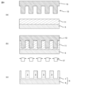
- FIG. (A) shows the structure 5 of the optical element 1 according to the second embodiment of the present invention
- (b) is a sectional view taken along the line AA in (a)
- (c) is a structure shown in (b).
- 2 is a cross-sectional view showing an optical element 1 obtained by forming a protective part 8 and a hard coat layer 9 on a body 5.
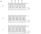
- FIG. (A) to (c) are cross-sectional views showing the manufacturing process of the optical element 1.
- (A)-(c) is sectional drawing which shows the manufacturing process of the optical element 1 following FIG.
- the optical element 1 connects a structure 5 having a plurality of convex shapes 3, and the convex shapes 3 to each other and is electrically conductive.
- a protection unit 8 made of metal or metal oxide is provided.
- a hard coat layer 9 that covers the protective portion 8 is laminated.
- the structure 5 has a plurality of convex shapes 3.
- the material of the structure 5 is not particularly limited, but is preferably formed of a transparent material.
- the structure 5 is not particularly limited as long as it has a plurality of convex shapes 3, for example, a transparent substrate 6 and a transparent resin layer 7 formed thereon and having a plurality of convex shapes 3. Consists of.
- the transparent substrate 6 is formed of a transparent material such as a resin substrate or a quartz substrate, and the material is not particularly limited, but is preferably a resin substrate.
- the resin constituting the resin base material examples include one selected from the group consisting of polyethylene terephthalate, polycarbonate, polyester, polyolefin, polyimide, polysulfone, polyethersulfone, cyclic polyolefin, and polyethylene naphthalate.
- the transparent substrate 6 is preferably in the form of a flexible film, and the thickness is preferably in the range of 25 to 500 ⁇ m.
- the transparent resin layer 7 can be formed by curing a photocurable resin composition.
- the convex shape 3 is an elongated convex shape (projection shape) or a pillar shape.
- the elongated convex shape 3 in order to exhibit a function as a polarizing plate, is formed so that a line and space shape is formed.
- the pitch at which the plurality of convex shapes 3 are formed is, for example, 10 nm to 1 ⁇ m, preferably 20 to 500 nm, more preferably 30 to 200 nm, and particularly preferably 40 to 120 nm.
- the value of (space width) / (line width) in the line and space shape is not particularly limited, but is, for example, 0.2 to 5, preferably 0.5 to 4, and more preferably 1 to 3.
- the aspect ratio of the convex shape 3 is not particularly limited, but is, for example, 1 to 5, preferably 1.5 to 4, and more preferably 2 to 3.
- the protection part 8 can be formed of a conductive metal (Ni, Al, etc.) or a metal oxide (ITO, etc.). As shown in FIG. 1, the protective portion 8 has a thickness that decreases toward the central portion C of two adjacent convex shapes 3, and a void portion S is formed in a region between the two adjacent convex shapes. It is formed so that. In the optical element 1 of the present embodiment, the protective portion 8 is not formed in a thin line shape, but is formed on the entire main surface or the side surface of the structure 5, but is formed so that the thickness decreases toward the central portion C. Therefore, the transmittance of the X-polarized component whose electric field vibration direction is the arrow X direction in FIG. 1 is higher than the transmittance of the Y-polarized light component whose electric field vibration direction is the arrow Y direction in FIG. For this reason, the optical element 1 functions as a polarizing plate on the same principle as a wire grid polarizing plate.
- t / T is preferably 0.5 or less, and preferably 0.3 or less.
- the lower limit of t / T is not particularly defined, but is 0.01, for example.
- the value of t / T is, for example, 0.01, 0.05, 0.1, 0.2, 0.3, 0.4, 0.5, and any of the numerical values exemplified here Or within a range between the two.
- the thickness t is preferably 50 nm or less. This is because if the thickness t is too large, the transmittance of the X-polarized light component in the central portion C becomes too small.
- the hard coat layer 9 is formed on the protective part 8.
- the hard coat layer 9 can be formed of metal, metal oxide, resin, or the like.
- the material of the hard coat layer 9 and the protective part 8 may be the same, but is preferably different.
- the hard coat layer 9 is a material having higher scratch resistance, wear resistance, and scratch resistance than the protective part 8. It is preferable to form by. In this case, it is possible to secure the polarizing function with the protection unit 8 and the scratch resistance with the hard coat layer 9.
- the hard coat layer 9 and the protective part 8 have different refractive indexes.
- the antireflection function can be secured by a combination of refractive indexes.
- the thickness of the hard coat layer 9 is not particularly limited, but is, for example, 1 nm to 5 m, preferably 10 nm to 1 ⁇ m, and preferably 50 to 500 nm.
- Second Embodiment An optical element 1 according to a second embodiment of the present invention is similar to the first embodiment, and the main difference is that the convex shape 3 is a pillar shape as shown in FIG. .
- the convex shape 3 By making the convex shape 3 into a pillar shape, it can be used as a light extraction member of a light emitting member such as an LED or an organic EL.
- the pillar shape is preferably a cylinder, and the diameter of the cylinder is preferably 50 to 200 nm.
- the pitch at which the plurality of convex shapes 3 are formed is, for example, 10 nm to 1 ⁇ m, preferably 20 to 500 nm, more preferably 30 to 200 nm, and particularly preferably 40 to 120 nm.
- the manufacturing method of the optical element 1 of this embodiment includes a transferred resin layer forming step, a transfer and curing step, a protective portion forming step, and a hard coat layer forming step.
- a photocurable resin composition is applied on the transparent substrate 6 to form the transferred resin layer 11.
- the photocurable resin composition constituting the transferred resin layer 11 contains a monomer and a photoinitiator and has a property of being cured by irradiation with active energy rays.
- Active energy rays is a general term for energy rays that can cure a photocurable resin composition, such as UV light, visible light, and electron beams.
- Monomers include photopolymerizable monomers for forming (meth) acrylic resins, styrene resins, olefin resins, polycarbonate resins, polyester resins, epoxy resins, silicone resins, etc., and photopolymerizable (meth) acrylic.
- System monomers are preferred.
- (meth) acryl means methacryl and / or acryl
- (meth) acrylate means methacrylate and / or acrylate.
- the photoinitiator is a component added to promote the polymerization of the monomer, and is preferably contained in an amount of 0.1 part by mass or more with respect to 100 parts by mass of the monomer.
- the upper limit of content of a photoinitiator is not prescribed
- the photocurable resin composition is a range in which components such as a solvent, a polymerization inhibitor, a chain transfer agent, an antioxidant, a photosensitizer, a filler, and a leveling agent do not affect the properties of the photocurable resin composition. May be included.
- the photocurable resin composition can be produced by mixing the above components by a known method.
- the photocurable resin composition can be applied onto the transparent substrate 6 by a method such as spin coating, spray coating, bar coating, dip coating, die coating, or slit coating to form the transferred resin layer 11. .
- the pressure for pressing the mold 13 against the transferred resin layer 11 may be any pressure that can transfer the shape of the reversal pattern 15 to the transferred resin layer 11.
- the active energy ray 17 applied to the transferred resin layer 11 may be irradiated with an integrated light amount sufficient to sufficiently cure the transferred resin layer 11, and the integrated light amount is, for example, 100 to 10,000 mJ / cm 2 .
- the transferred resin layer 11 is cured by irradiation with the active energy ray 17.
- the active energy ray 17 is irradiated from the transparent substrate 6 side, but the active energy ray 17 may be irradiated from the mold side.
- the structure 5 in which the transparent resin layer 7 having a plurality of convex shapes 3 is formed on the transparent substrate 6 is obtained.
- the uncured photocurable resin composition may be washed away with a solvent.
- the protection part 8 is formed on the transparent resin layer 7 as shown in FIGS.
- the protection part 8 can be formed, for example, by depositing a conductive metal or metal oxide as a material on the transparent resin layer 7 by an isotropic film formation method such as sputtering. Since the atoms ejected from the target during sputtering are likely to adhere to the tip of the convex shape 3, the thickness of the protective portion 8 preferentially increases in the vicinity of the tip of the convex shape 3 as shown in FIG. Thus, a growth portion 8a like the tip of a match stick is formed. When the film formation is further continued, the growth portions 8a grown from the tips of the respective convex shapes 3 are bonded to each other to have the shape shown in FIG.
- the width of the gap S is preferably in the range of 25 to 90%, more preferably in the range of 40 to 85% with respect to the pitch at which two adjacent convex shapes are formed.
- the hard coat layer 9 is formed on the protective portion 8, and the manufacture of the optical element 1 is completed.
- the hard coat layer 9 is formed by, for example, a method of forming a metal or metal oxide layer by sputtering, vapor deposition, or the like, bonding a resin film, or applying and curing a photocurable resin composition. Can do.
Landscapes
- Physics & Mathematics (AREA)
- General Physics & Mathematics (AREA)
- Optics & Photonics (AREA)
- Polarising Elements (AREA)
- Surface Treatment Of Optical Elements (AREA)
Abstract
凸形状の倒壊をより確実に抑制することができる光学素子を提供する。 本発明によれば、複数の凸形状を有する構造体と、前記凸形状同士を連結し且つ導電性の金属又は金属酸化物からなる保護部を備え、前記保護部は、隣接した2つの前記凸形状の中央部に向かって厚さが薄くなり且つ隣接した2つの前記凸形状の間の領域に空隙部が形成されるように形成される、光学素子が提供される。
Description
本発明は、光学素子及び偏光板に関する。
特許文献1には、 構造体上の樹脂皮膜に複数の細長い凸形状を形成し、その上に金属膜を蒸着することによってワイヤグリッド偏光板を製造する技術が開示されている。
このような構成の偏光板では、凸形状の倒壊が起こりやすいので、特許文献2では、凸形状の倒壊を防ぐべく、凸形状同士を互いに連結するように保護層を形成している。
このような構成の偏光板では、凸形状の倒壊が起こりやすいので、特許文献2では、凸形状の倒壊を防ぐべく、凸形状同士を互いに連結するように保護層を形成している。
しかし、特許文献2の方法では、凸形状を形成した後に、金属層を形成してパターニングし、その後、保護層を形成する必要があるので、凸形状の形成後に保護層を形成完了までの工程数が多いので、その間に凸形状の倒壊が起こる場合がある。
本発明はこのような事情に鑑みてなされたものであり、凸形状の倒壊をより確実に抑制することができる光学素子を提供するものである。
本発明によれば、複数の凸形状を有する構造体と、前記凸形状同士を連結し且つ導電性の金属又は金属酸化物からなる保護部を備え、前記保護部は、隣接した2つの前記凸形状の中央部に向かって厚さが薄くなり且つ隣接した2つの前記凸形状の間の領域に空隙部が形成されるように形成される、光学素子が提供される。
本発明の光学素子は、導電性の金属又は金属酸化物で凸形状同士を連結して保護部を構成している。このため、凸形状の形成直後に保護部を形成することができるので、凸形状の倒壊を従来技術よりも確実に抑制することができる。また、この保護部は、隣接した2つの凸形状の中央部に向かって厚さが薄くなり且つ隣接した2つの前記凸形状の間の領域に空隙部が形成されるように形成されているので、偏光機能が発揮されることが実験で確認された。
以下、本発明の種々の実施形態を例示する。以下に示す実施形態は、互いに組み合わせ可能である。
好ましくは、前記空隙部の幅は、隣接した2つの凸形状が形成されるピッチに対して、25~90%の範囲内である。
好ましくは、前記保護部は、前記凸形状の先端を起点として導電性の金属又は金属酸化物を付着させることによって形成される。
好ましくは、前記保護部を被覆するハードコート層が積層されている。
好ましくは、前記ハードコート層と前記保護部は、屈折率が異なる。
本発明の別の観点によれば、上記光学素子からなる偏光板が提供される。
好ましくは、前記空隙部の幅は、隣接した2つの凸形状が形成されるピッチに対して、25~90%の範囲内である。
好ましくは、前記保護部は、前記凸形状の先端を起点として導電性の金属又は金属酸化物を付着させることによって形成される。
好ましくは、前記保護部を被覆するハードコート層が積層されている。
好ましくは、前記ハードコート層と前記保護部は、屈折率が異なる。
本発明の別の観点によれば、上記光学素子からなる偏光板が提供される。
以下、図面を参照しながら本発明の好ましい実施の形態について具体的に説明する。
1.光学素子
1-1.第1実施形態
本発明の第1実施形態の光学素子1は、図1~図2に示すように、複数の凸形状3を有する構造体5と、凸形状3同士を連結し且つ導電性の金属又は金属酸化物からなる保護部8を備える。また、保護部8を被覆するハードコート層9が積層されている。
1-1.第1実施形態
本発明の第1実施形態の光学素子1は、図1~図2に示すように、複数の凸形状3を有する構造体5と、凸形状3同士を連結し且つ導電性の金属又は金属酸化物からなる保護部8を備える。また、保護部8を被覆するハードコート層9が積層されている。
<構造体5>
構造体5は、複数の凸形状3を有する。構造体5の材質は特に限定されないが、透明材料で形成することが好ましい。構造体5は、複数の凸形状3を有するものであればその構成は特に限定されないが、例えば、透明基材6と、その上に形成され且つ複数の凸形状3を有する透明樹脂層7とで構成される。透明基材6は、樹脂基材、石英基材などの透明材料で形成され、その材質は、特に限定されないが、樹脂基材であることが好ましい。樹脂基材を構成する樹脂としては、例えば、ポリエチレンテレフタレート、ポリカーボネート、ポリエステル、ポリオレフィン、ポリイミド、ポリサルフォン、ポリエーテルサルフォン、環状ポリオレフィンおよびポリエチレンナフタレートからなる群から選ばれる1種からなるものである。また、透明基材6は可撓性を有するフィルム状であることが好ましく、その厚さは25~500μmの範囲であることが好ましい。透明樹脂層7は、光硬化性樹脂組成物を硬化させて形成することができる。
構造体5は、複数の凸形状3を有する。構造体5の材質は特に限定されないが、透明材料で形成することが好ましい。構造体5は、複数の凸形状3を有するものであればその構成は特に限定されないが、例えば、透明基材6と、その上に形成され且つ複数の凸形状3を有する透明樹脂層7とで構成される。透明基材6は、樹脂基材、石英基材などの透明材料で形成され、その材質は、特に限定されないが、樹脂基材であることが好ましい。樹脂基材を構成する樹脂としては、例えば、ポリエチレンテレフタレート、ポリカーボネート、ポリエステル、ポリオレフィン、ポリイミド、ポリサルフォン、ポリエーテルサルフォン、環状ポリオレフィンおよびポリエチレンナフタレートからなる群から選ばれる1種からなるものである。また、透明基材6は可撓性を有するフィルム状であることが好ましく、その厚さは25~500μmの範囲であることが好ましい。透明樹脂層7は、光硬化性樹脂組成物を硬化させて形成することができる。
凸形状3は、細長い凸形状(凸条形状)またはピラー形状である。本実施形態では、偏光板として機能を発揮させるために、ラインアンドスペース形状が形成されるように細長い凸形状3を形成している。複数の凸形状3が形成されるピッチは、例えば10nm~1μmであり、20~500nmが好ましく、30~200nmがさらに好ましく、40~120nmがとりわけ好ましい。ラインアンドスペース形状の(スペースの幅)/(ラインの幅)の値は、特に限定されないが、例えば0.2~5であり、0.5~4が好ましく、1~3がさらに好ましい。小さすぎると構造体5と保護部8とで取り囲む領域に空隙部Sが形成されにくくなり、大きすぎると凸形状3同士を連結する保護部8の形成が困難になる。凸形状3のアスペクト比は、特に限定されないが、例えば、1~5であり、1.5~4が好ましく、2~3がさらに好ましい。
<保護部8>
保護部8は、導電性の金属(Ni,Alなど)又は金属酸化物(ITOなど)で形成することができる。保護部8は、図1に示すように、隣接した2つの凸形状3の中央部Cに向かって厚さが薄くなり且つ隣接した2つの前記凸形状の間の領域に空隙部Sが形成されるように形成される。本実施形態の光学素子1では、保護部8は細線状ではなく、構造体5の主面の全面、あるいは側面に形成されているが、中央部Cに向かって厚さが薄くなるように形成されているので、電場の振動方向が図1の矢印X方向であるX偏光成分の透過率が、電場の振動方向が図1の矢印Y方向であるY偏光成分の透過率よりも高くなる。このため、光学素子1は、ワイヤグリッド偏光板と同様の原理によって、偏光板として機能する。
保護部8は、導電性の金属(Ni,Alなど)又は金属酸化物(ITOなど)で形成することができる。保護部8は、図1に示すように、隣接した2つの凸形状3の中央部Cに向かって厚さが薄くなり且つ隣接した2つの前記凸形状の間の領域に空隙部Sが形成されるように形成される。本実施形態の光学素子1では、保護部8は細線状ではなく、構造体5の主面の全面、あるいは側面に形成されているが、中央部Cに向かって厚さが薄くなるように形成されているので、電場の振動方向が図1の矢印X方向であるX偏光成分の透過率が、電場の振動方向が図1の矢印Y方向であるY偏光成分の透過率よりも高くなる。このため、光学素子1は、ワイヤグリッド偏光板と同様の原理によって、偏光板として機能する。
図1に示すように保護部8の全体の厚さをT、中央部C(最も薄い部位)での厚さをtとすると、t/Tの値が小さいほど、保護部8が偏光機能を適切に発揮し、t/Tは、0.5以下が好ましく、0.3以下が好ましい。t/Tの下限は、特に規定されないが、例えば、0.01である。t/Tの値は、具体的には例えば、0.01、0.05、0.1、0.2、0.3、0.4、0.5であり、ここで例示した数値の何れか2つの間の範囲内であってもよい。また、厚さtは、50nm以下が好ましい。厚さtが大きすぎると中央部CにおけるX偏光成分の透過率が小さくなりすぎるからである。
<ハードコート層9>
ハードコート層9は、保護部8上に形成する。ハードコート層9は、金属、金属酸化物、樹脂などで形成することができる。本実施形態では、凸形状3同士を連結するように保護部8を形成しているので、ハードコート層9を形成する際の凸形状3の倒壊が抑制される。ハードコート層9と保護部8の材料は同じであってもよいが、異なることが好ましく、ハードコート層9は、保護部8よりも耐擦傷性、耐摩耗性、及び耐傷つき性が高い材料で形成することが好ましい。この場合、保護部8で偏光機能を担保し、ハードコート層9で耐擦傷性を担保することが可能になる。また、ハードコート層9と保護部8は、屈折率が互いに異なることが好ましい。この場合、屈折率の組み合わせにより、反射防止機能を担保できるという利点がある。ハードコート層9の厚さは、特に規定されないが、例えば、1nm~5mであり、10nm~1μmが好ましく、50~500nmが好ましい。
ハードコート層9は、保護部8上に形成する。ハードコート層9は、金属、金属酸化物、樹脂などで形成することができる。本実施形態では、凸形状3同士を連結するように保護部8を形成しているので、ハードコート層9を形成する際の凸形状3の倒壊が抑制される。ハードコート層9と保護部8の材料は同じであってもよいが、異なることが好ましく、ハードコート層9は、保護部8よりも耐擦傷性、耐摩耗性、及び耐傷つき性が高い材料で形成することが好ましい。この場合、保護部8で偏光機能を担保し、ハードコート層9で耐擦傷性を担保することが可能になる。また、ハードコート層9と保護部8は、屈折率が互いに異なることが好ましい。この場合、屈折率の組み合わせにより、反射防止機能を担保できるという利点がある。ハードコート層9の厚さは、特に規定されないが、例えば、1nm~5mであり、10nm~1μmが好ましく、50~500nmが好ましい。
1-2.第2実施形態
本発明の第2実施形態の光学素子1は、第1実施形態に類似しており、図3に示すように、凸形状3がピラー形状である点が主な相違点である。
本発明の第2実施形態の光学素子1は、第1実施形態に類似しており、図3に示すように、凸形状3がピラー形状である点が主な相違点である。
凸形状3をピラー形状にすることによって、LEDや有機ELなどの発光部材の光取り出し部材として利用可能である。ピラー形状としては円柱が好ましく、円柱の直径は50~200nmが好ましい。複数の凸形状3が形成されるピッチは、例えば10nm~1μmであり、20~500nmが好ましく、30~200nmがさらに好ましく、40~120nmがとりわけ好ましい。
2.光学素子1の製造方法
次に、図4~図5を用いて、光学素子1の製造方法について説明する。本実施形態の光学素子1の製造方法は、被転写樹脂層形成工程、転写及び硬化工程、保護部形成工程、及びハードコート層形成工程を備える。
次に、図4~図5を用いて、光学素子1の製造方法について説明する。本実施形態の光学素子1の製造方法は、被転写樹脂層形成工程、転写及び硬化工程、保護部形成工程、及びハードコート層形成工程を備える。
(1)被転写樹脂層形成工程
図4(a)に示すように、透明基材6上に光硬化性樹脂組成物を塗布して被転写樹脂層11を形成する。被転写樹脂層11を構成する光硬化性樹脂組成物は、モノマーと、光開始剤を含有し、活性エネルギー線の照射によって硬化する性質を有する。「活性エネルギー線」は、UV光、可視光、電子線などの、光硬化性樹脂組成物を硬化可能なエネルギー線の総称である。
図4(a)に示すように、透明基材6上に光硬化性樹脂組成物を塗布して被転写樹脂層11を形成する。被転写樹脂層11を構成する光硬化性樹脂組成物は、モノマーと、光開始剤を含有し、活性エネルギー線の照射によって硬化する性質を有する。「活性エネルギー線」は、UV光、可視光、電子線などの、光硬化性樹脂組成物を硬化可能なエネルギー線の総称である。
モノマーとしては、(メタ)アクリル樹脂、スチレン樹脂、オレフィン樹脂、ポリカーボネート樹脂、ポリエステル樹脂、エポキシ樹脂、シリコーン樹脂等を形成するための光重合性のモノマーが挙げられ、光重合性の(メタ)アクリル系モノマーが好ましい。なお、本明細書において、(メタ)アクリルとは、メタクリルおよび/またはアクリルを意味し、(メタ)アクリレートはメタクリレートおよび/またはアクリレートを意味する。
光開始剤は、モノマーの重合を促進するために添加される成分であり、前記モノマー100質量部に対して0.1質量部以上含有されることが好ましい。光開始剤の含有量の上限は、特に規定されないが、例えば前記モノマー100質量部に対して20質量部である。
光硬化性樹脂組成物は、溶剤、重合禁止剤、連鎖移動剤、酸化防止剤、光増感剤、充填剤、レベリング剤等の成分を光硬化性樹脂組成物の性質に影響を与えない範囲で含んでいてもよい。
光硬化性樹脂組成物は、上記成分を公知の方法で混合することにより製造することができる。光硬化性樹脂組成物は、スピンコート、スプレーコート、バーコート、ディップコート、ダイコートおよびスリットコート等の方法で透明基材6上に塗布して被転写樹脂層11を形成することが可能である。
(2)転写及び硬化工程
次に、図4(a)~(b)に示すように、被転写樹脂層11に対して、凸形状3の反転パターン15を有するモールド13を押し付けた状態で被転写樹脂層11に活性エネルギー線17を照射して被転写樹脂層11を硬化させて透明樹脂層7を形成する。
次に、図4(a)~(b)に示すように、被転写樹脂層11に対して、凸形状3の反転パターン15を有するモールド13を押し付けた状態で被転写樹脂層11に活性エネルギー線17を照射して被転写樹脂層11を硬化させて透明樹脂層7を形成する。
モールド13を被転写樹脂層11に押し付ける圧力は、反転パターン15の形状を被転写樹脂層11に転写可能な圧力であればよい。被転写樹脂層11へ照射する活性エネルギー線17は、被転写樹脂層11が十分に硬化する程度の積算光量で照射すればよく、積算光量は、例えば100~10000mJ/cm2である。活性エネルギー線17の照射によって、被転写樹脂層11が硬化される。本実施形態では、透明基材6側から活性エネルギー線17の照射を行っているが、モールド側から活性エネルギー線17の照射を行ってもよい。
次に、モールド13を取り外すことによって、図4(c)に示すように、透明基材6上に複数の凸形状3を有する透明樹脂層7が形成された構造体5が得られる。なお、モールド13を取り外すときに、未硬化の光硬化性樹脂組成物を溶剤で洗い流してもよい。
(3)保護部形成工程
次に、図5(a)~(b)に示すように、透明樹脂層7上に保護部8を形成する。保護部8は、例えば、材料となる導電性の金属又は金属酸化物をスパッタリングなどの等方性成膜法によって透明樹脂層7上に付着させることによって形成することができる。スパッタリングの際にターゲットからはじき出された原子は凸形状3の先端に付着しやすいので、図5(a)に示すように、凸形状3の先端近傍において保護部8の厚さが優先的に増大してマッチ棒の先端のような成長部8aが形成される。そして、さらに成膜を続けると、各凸形状3の先端から成長した成長部8aが互いにくっついて図5(b)に示す形状になり、保護部8の形成が完了する。成長部8a同士がくっつくと、成長部8aの下側の領域には金属又は金属酸化物の原子が付着しないので、この領域に空隙部Sが形成される。空隙部Sの幅は、隣接した2つの凸形状が形成されるピッチに対して、好ましくは25~90%の範囲内であり、40~85%の範囲内がより好ましい。空隙部Sの幅をこの範囲内に制御することによって、保護部やハードコート層とは異なる屈折率層としての機能を発揮しやすくなる。
次に、図5(a)~(b)に示すように、透明樹脂層7上に保護部8を形成する。保護部8は、例えば、材料となる導電性の金属又は金属酸化物をスパッタリングなどの等方性成膜法によって透明樹脂層7上に付着させることによって形成することができる。スパッタリングの際にターゲットからはじき出された原子は凸形状3の先端に付着しやすいので、図5(a)に示すように、凸形状3の先端近傍において保護部8の厚さが優先的に増大してマッチ棒の先端のような成長部8aが形成される。そして、さらに成膜を続けると、各凸形状3の先端から成長した成長部8aが互いにくっついて図5(b)に示す形状になり、保護部8の形成が完了する。成長部8a同士がくっつくと、成長部8aの下側の領域には金属又は金属酸化物の原子が付着しないので、この領域に空隙部Sが形成される。空隙部Sの幅は、隣接した2つの凸形状が形成されるピッチに対して、好ましくは25~90%の範囲内であり、40~85%の範囲内がより好ましい。空隙部Sの幅をこの範囲内に制御することによって、保護部やハードコート層とは異なる屈折率層としての機能を発揮しやすくなる。
(4)ハードコート層形成工程
次に、図5(c)に示すように、保護部8上にハードコート層9を形成して、光学素子1の製造が完了する。ハードコート層9は、例えば、スパッタリングや蒸着などによって金属又は金属酸化物層を形成したり、樹脂フィルムを貼り合わせたり、光硬化性樹脂組成物を塗布して硬化したりする方法によって形成することができる。
次に、図5(c)に示すように、保護部8上にハードコート層9を形成して、光学素子1の製造が完了する。ハードコート層9は、例えば、スパッタリングや蒸着などによって金属又は金属酸化物層を形成したり、樹脂フィルムを貼り合わせたり、光硬化性樹脂組成物を塗布して硬化したりする方法によって形成することができる。
1:光学素子、3:凸形状、5:構造体、6:透明基材、7:透明樹脂層、8:保護部、9:ハードコート層、11:被転写樹脂層、13:モールド、15:反転パターン、17:活性エネルギー線
Claims (6)
- 複数の凸形状を有する構造体と、前記凸形状同士を連結し且つ導電性の金属又は金属酸化物からなる保護部を備え、
前記保護部は、隣接した2つの前記凸形状の中央部に向かって厚さが薄くなり且つ隣接した2つの前記凸形状の間の領域に空隙部が形成されるように形成される、光学素子。 - 前記空隙部の幅は、隣接した2つの凸形状が形成されるピッチに対して、25~90%の範囲内である、請求項1に記載の光学素子
- 前記保護部は、前記凸形状の先端を起点として導電性の金属又は金属酸化物を付着させることによって形成される、請求項1又は請求項2に記載の光学素子。
- 前記保護部を被覆するハードコート層が積層されている、請求項1~請求項3の何れかの1つに記載の光学素子。
- 前記ハードコート層と前記保護部は、屈折率が異なる、請求項4に記載の光学素子。
- 請求項1~請求項5の何れか1つに記載の光学素子からなる偏光板。
Applications Claiming Priority (2)
| Application Number | Priority Date | Filing Date | Title |
|---|---|---|---|
| JP2015078456A JP2018100986A (ja) | 2015-04-07 | 2015-04-07 | 光学素子及び偏光板 |
| JP2015-078456 | 2015-04-07 |
Publications (1)
| Publication Number | Publication Date |
|---|---|
| WO2016163390A1 true WO2016163390A1 (ja) | 2016-10-13 |
Family
ID=57071995
Family Applications (1)
| Application Number | Title | Priority Date | Filing Date |
|---|---|---|---|
| PCT/JP2016/061251 Ceased WO2016163390A1 (ja) | 2015-04-07 | 2016-04-06 | 光学素子及び偏光板 |
Country Status (3)
| Country | Link |
|---|---|
| JP (1) | JP2018100986A (ja) |
| TW (1) | TW201643481A (ja) |
| WO (1) | WO2016163390A1 (ja) |
Cited By (2)
| Publication number | Priority date | Publication date | Assignee | Title |
|---|---|---|---|---|
| WO2018105586A1 (ja) * | 2016-12-06 | 2018-06-14 | Scivax株式会社 | 光学部材および当該光学部材を用いた液晶パネル、並びにそれらの製造方法 |
| CN115917377A (zh) * | 2020-05-25 | 2023-04-04 | 迪睿合株式会社 | 偏光板及其制造方法、以及光学设备 |
Families Citing this family (1)
| Publication number | Priority date | Publication date | Assignee | Title |
|---|---|---|---|---|
| WO2023283913A1 (zh) * | 2021-07-16 | 2023-01-19 | 福建晶安光电有限公司 | 偏振元件、发光二极管以及发光装置 |
Citations (3)
| Publication number | Priority date | Publication date | Assignee | Title |
|---|---|---|---|---|
| JP2006003447A (ja) * | 2004-06-15 | 2006-01-05 | Sony Corp | 偏光分離素子及びその製造方法 |
| JP2007121507A (ja) * | 2005-10-26 | 2007-05-17 | Nippon Zeon Co Ltd | 光学部材及び光学部材の製法 |
| JP2010049280A (ja) * | 2009-11-25 | 2010-03-04 | Seiko Epson Corp | 偏光素子の製造方法 |
-
2015
- 2015-04-07 JP JP2015078456A patent/JP2018100986A/ja active Pending
-
2016
- 2016-04-06 TW TW105110732A patent/TW201643481A/zh unknown
- 2016-04-06 WO PCT/JP2016/061251 patent/WO2016163390A1/ja not_active Ceased
Patent Citations (3)
| Publication number | Priority date | Publication date | Assignee | Title |
|---|---|---|---|---|
| JP2006003447A (ja) * | 2004-06-15 | 2006-01-05 | Sony Corp | 偏光分離素子及びその製造方法 |
| JP2007121507A (ja) * | 2005-10-26 | 2007-05-17 | Nippon Zeon Co Ltd | 光学部材及び光学部材の製法 |
| JP2010049280A (ja) * | 2009-11-25 | 2010-03-04 | Seiko Epson Corp | 偏光素子の製造方法 |
Cited By (3)
| Publication number | Priority date | Publication date | Assignee | Title |
|---|---|---|---|---|
| WO2018105586A1 (ja) * | 2016-12-06 | 2018-06-14 | Scivax株式会社 | 光学部材および当該光学部材を用いた液晶パネル、並びにそれらの製造方法 |
| CN115917377A (zh) * | 2020-05-25 | 2023-04-04 | 迪睿合株式会社 | 偏光板及其制造方法、以及光学设备 |
| US12449581B2 (en) | 2020-05-25 | 2025-10-21 | Dexerials Corporation | Polarizing plate, method of manufacturing the same and optical apparatus |
Also Published As
| Publication number | Publication date |
|---|---|
| JP2018100986A (ja) | 2018-06-28 |
| TW201643481A (zh) | 2016-12-16 |
Similar Documents
| Publication | Publication Date | Title |
|---|---|---|
| CN111033118B (zh) | 衍射导光板和制造衍射导光板的方法 | |
| CN108474878B (zh) | 衍射光学元件和光照射装置 | |
| TW201307086A (zh) | 顯示裝置及製造其之方法 | |
| KR100974204B1 (ko) | 충격에 강한 와이어 그리드 편광판 및 그 제조 방법 | |
| WO2016163390A1 (ja) | 光学素子及び偏光板 | |
| CN103730601A (zh) | 分布布拉格反射镜结构及制备方法和有机发光二极管结构 | |
| JP6603218B2 (ja) | 微細構造体の製造方法 | |
| US20170315281A1 (en) | Polarizing plate, method for manufacturing same, and medium | |
| US11123960B2 (en) | Film mold and imprinting method | |
| JP2017126064A (ja) | 回折光学素子、及び光照射装置 | |
| BR112016018273B1 (pt) | Método para a formação de um polarizador, método para a formação de um artigo oftálmico polarizado e lente oftálmica polarizada moldada | |
| JP2012118520A (ja) | 微細凹凸パタン基材 | |
| TW201609414A (zh) | 偏光板、高亮度偏光板及ips模式液晶顯示裝置 | |
| JP5821207B2 (ja) | ハードコートフィルム及びハードコートフィルムの製造方法 | |
| WO2016195064A1 (ja) | 構造体及びその製造方法 | |
| JP6293990B2 (ja) | 光学フィルム、光学フィルム用転写体、画像表示装置及び光学フィルムの製造用金型 | |
| WO2017078019A1 (ja) | 微細構造体の製造方法 | |
| JP6440333B1 (ja) | Rfidタグ及びrfidタグの製造方法 | |
| CN106681546A (zh) | 触控装置及其制造方法 | |
| JP2006263975A (ja) | 光学素子の製造方法 | |
| KR101352055B1 (ko) | 일체형 광학 필름 제조 방법 및 일체형 광학 필름 | |
| JP2018046182A (ja) | 構造体の製造方法 | |
| WO2016043244A1 (ja) | 微細パターン付き繊維体 | |
| JP2012203091A (ja) | 導電性素子およびその製造方法 | |
| TW202407389A (zh) | 具物理性成型偏振微小結構之變色光學透鏡裝置及其製造方法 |
Legal Events
| Date | Code | Title | Description |
|---|---|---|---|
| 121 | Ep: the epo has been informed by wipo that ep was designated in this application |
Ref document number: 16776556 Country of ref document: EP Kind code of ref document: A1 |
|
| NENP | Non-entry into the national phase |
Ref country code: DE |
|
| 122 | Ep: pct application non-entry in european phase |
Ref document number: 16776556 Country of ref document: EP Kind code of ref document: A1 |
|
| NENP | Non-entry into the national phase |
Ref country code: JP |