WO2016163242A1 - 固体撮像素子および電子機器 - Google Patents
固体撮像素子および電子機器 Download PDFInfo
- Publication number
- WO2016163242A1 WO2016163242A1 PCT/JP2016/059323 JP2016059323W WO2016163242A1 WO 2016163242 A1 WO2016163242 A1 WO 2016163242A1 JP 2016059323 W JP2016059323 W JP 2016059323W WO 2016163242 A1 WO2016163242 A1 WO 2016163242A1
- Authority
- WO
- WIPO (PCT)
- Prior art keywords
- pixel
- wiring
- light
- solid
- symmetric
- Prior art date
- Legal status (The legal status is an assumption and is not a legal conclusion. Google has not performed a legal analysis and makes no representation as to the accuracy of the status listed.)
- Ceased
Links
Images




Classifications
-
- H—ELECTRICITY
- H10—SEMICONDUCTOR DEVICES; ELECTRIC SOLID-STATE DEVICES NOT OTHERWISE PROVIDED FOR
- H10F—INORGANIC SEMICONDUCTOR DEVICES SENSITIVE TO INFRARED RADIATION, LIGHT, ELECTROMAGNETIC RADIATION OF SHORTER WAVELENGTH OR CORPUSCULAR RADIATION
- H10F39/00—Integrated devices, or assemblies of multiple devices, comprising at least one element covered by group H10F30/00, e.g. radiation detectors comprising photodiode arrays
- H10F39/80—Constructional details of image sensors
- H10F39/811—Interconnections
-
- H—ELECTRICITY
- H04—ELECTRIC COMMUNICATION TECHNIQUE
- H04N—PICTORIAL COMMUNICATION, e.g. TELEVISION
- H04N25/00—Circuitry of solid-state image sensors [SSIS]; Control thereof
- H04N25/10—Circuitry of solid-state image sensors [SSIS]; Control thereof for transforming different wavelengths into image signals
- H04N25/11—Arrangement of colour filter arrays [CFA]; Filter mosaics
- H04N25/13—Arrangement of colour filter arrays [CFA]; Filter mosaics characterised by the spectral characteristics of the filter elements
- H04N25/134—Arrangement of colour filter arrays [CFA]; Filter mosaics characterised by the spectral characteristics of the filter elements based on three different wavelength filter elements
-
- H—ELECTRICITY
- H04—ELECTRIC COMMUNICATION TECHNIQUE
- H04N—PICTORIAL COMMUNICATION, e.g. TELEVISION
- H04N25/00—Circuitry of solid-state image sensors [SSIS]; Control thereof
- H04N25/70—SSIS architectures; Circuits associated therewith
-
- H—ELECTRICITY
- H10—SEMICONDUCTOR DEVICES; ELECTRIC SOLID-STATE DEVICES NOT OTHERWISE PROVIDED FOR
- H10F—INORGANIC SEMICONDUCTOR DEVICES SENSITIVE TO INFRARED RADIATION, LIGHT, ELECTROMAGNETIC RADIATION OF SHORTER WAVELENGTH OR CORPUSCULAR RADIATION
- H10F39/00—Integrated devices, or assemblies of multiple devices, comprising at least one element covered by group H10F30/00, e.g. radiation detectors comprising photodiode arrays
- H10F39/10—Integrated devices
- H10F39/12—Image sensors
- H10F39/199—Back-illuminated image sensors
-
- H—ELECTRICITY
- H10—SEMICONDUCTOR DEVICES; ELECTRIC SOLID-STATE DEVICES NOT OTHERWISE PROVIDED FOR
- H10F—INORGANIC SEMICONDUCTOR DEVICES SENSITIVE TO INFRARED RADIATION, LIGHT, ELECTROMAGNETIC RADIATION OF SHORTER WAVELENGTH OR CORPUSCULAR RADIATION
- H10F39/00—Integrated devices, or assemblies of multiple devices, comprising at least one element covered by group H10F30/00, e.g. radiation detectors comprising photodiode arrays
- H10F39/80—Constructional details of image sensors
- H10F39/805—Coatings
- H10F39/8057—Optical shielding
-
- H—ELECTRICITY
- H10—SEMICONDUCTOR DEVICES; ELECTRIC SOLID-STATE DEVICES NOT OTHERWISE PROVIDED FOR
- H10F—INORGANIC SEMICONDUCTOR DEVICES SENSITIVE TO INFRARED RADIATION, LIGHT, ELECTROMAGNETIC RADIATION OF SHORTER WAVELENGTH OR CORPUSCULAR RADIATION
- H10F39/00—Integrated devices, or assemblies of multiple devices, comprising at least one element covered by group H10F30/00, e.g. radiation detectors comprising photodiode arrays
- H10F39/80—Constructional details of image sensors
- H10F39/806—Optical elements or arrangements associated with the image sensors
-
- H—ELECTRICITY
- H10—SEMICONDUCTOR DEVICES; ELECTRIC SOLID-STATE DEVICES NOT OTHERWISE PROVIDED FOR
- H10F—INORGANIC SEMICONDUCTOR DEVICES SENSITIVE TO INFRARED RADIATION, LIGHT, ELECTROMAGNETIC RADIATION OF SHORTER WAVELENGTH OR CORPUSCULAR RADIATION
- H10F39/00—Integrated devices, or assemblies of multiple devices, comprising at least one element covered by group H10F30/00, e.g. radiation detectors comprising photodiode arrays
- H10F39/80—Constructional details of image sensors
- H10F39/806—Optical elements or arrangements associated with the image sensors
- H10F39/8067—Reflectors
-
- H—ELECTRICITY
- H10—SEMICONDUCTOR DEVICES; ELECTRIC SOLID-STATE DEVICES NOT OTHERWISE PROVIDED FOR
- H10F—INORGANIC SEMICONDUCTOR DEVICES SENSITIVE TO INFRARED RADIATION, LIGHT, ELECTROMAGNETIC RADIATION OF SHORTER WAVELENGTH OR CORPUSCULAR RADIATION
- H10F39/00—Integrated devices, or assemblies of multiple devices, comprising at least one element covered by group H10F30/00, e.g. radiation detectors comprising photodiode arrays
- H10F39/10—Integrated devices
- H10F39/12—Image sensors
- H10F39/18—Complementary metal-oxide-semiconductor [CMOS] image sensors; Photodiode array image sensors
- H10F39/182—Colour image sensors
-
- H—ELECTRICITY
- H10—SEMICONDUCTOR DEVICES; ELECTRIC SOLID-STATE DEVICES NOT OTHERWISE PROVIDED FOR
- H10F—INORGANIC SEMICONDUCTOR DEVICES SENSITIVE TO INFRARED RADIATION, LIGHT, ELECTROMAGNETIC RADIATION OF SHORTER WAVELENGTH OR CORPUSCULAR RADIATION
- H10F39/00—Integrated devices, or assemblies of multiple devices, comprising at least one element covered by group H10F30/00, e.g. radiation detectors comprising photodiode arrays
- H10F39/80—Constructional details of image sensors
- H10F39/805—Coatings
- H10F39/8053—Colour filters
Definitions
- the present disclosure relates to a solid-state imaging device and an electronic device, and more particularly, to a solid-state imaging device and an electronic device that can eliminate asymmetry of the amount of received light according to the incident angle of light incident on a pixel.
- a solid-state imaging device such as a CCD (Charge Coupled Device) or a CMOS (Complementary Metal Oxide Semiconductor) image sensor is used.
- the solid-state imaging device has a pixel in which a photodiode that performs photoelectric conversion and a plurality of transistors are combined, and outputs a pixel signal that is output from a plurality of pixels arranged on an image plane on which an object image is formed. Based on this, an image is constructed.
- a backside illumination type solid-state imaging device light incident from the backside may be transmitted through the semiconductor substrate and reflected by the wiring formed in the wiring layer, and the reflected light may enter the photodiode.
- the wiring formed in the wiring layer is formed in an asymmetric shape with respect to the center of the pixel, the amount of reflected light incident on the photodiode may change according to the incident angle of light. there were. In other words, in this case, even if light with a constant amount of light enters the pixel while changing the incident angle, the amount of reflected light incident on the photodiode changes due to the asymmetry of the wiring layout. There were times when it was not.
- Patent Document 1 adopts a wiring layout in which no wiring is arranged below a pixel that receives light having a long wavelength that easily passes through a semiconductor substrate, and reduces reflection of light in a wiring layer.
- a back-illuminated solid-state imaging device that suppresses the mixing of light is disclosed.
- the present disclosure has been made in view of such a situation, and makes it possible to eliminate asymmetry of the amount of received light according to the incident angle of light incident on a pixel.
- a solid-state imaging device includes a pixel having a light receiving unit that receives light incident from the back side of a semiconductor substrate, and a wiring layer stacked on the surface of the semiconductor substrate, When the pixel is viewed in plan, it has a symmetrical wiring formed in a symmetrical shape with respect to the center of the pixel.
- An electronic apparatus includes a pixel having a light receiving portion that receives light incident from the back side of a semiconductor substrate, and a wiring layer stacked on the surface of the semiconductor substrate, and the pixel includes the pixel ,
- a solid-state imaging device having a symmetric wiring formed in a symmetrical shape with respect to the center of the pixel.
- the pixel includes a pixel having a light receiving portion that receives light incident from the back surface side of the semiconductor substrate, and a wiring layer stacked on the surface of the semiconductor substrate.
- a symmetrical wiring having a symmetrical shape with respect to the center of the pixel is formed.
- the asymmetry of the amount of received light according to the incident angle of light incident on the pixel can be eliminated.
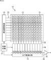
- FIG. 1 is a block diagram illustrating a configuration example of an embodiment of an image sensor to which the present technology is applied.
- the image sensor 11 includes a pixel region 12, a vertical drive circuit 13, a column signal processing circuit 14, a horizontal drive circuit 15, an output circuit 16, and a control circuit 17.
- the pixel region 12 is a light receiving surface that receives light collected by an optical system (not shown).
- a plurality of pixels 21 are arranged in a matrix in the pixel region 12, and each pixel 21 is connected to the vertical drive circuit 13 for each row via a horizontal signal line 22, and the vertical signal line 23 is connected to the pixel region 12.
- the plurality of pixels 21 each output a pixel signal at a level corresponding to the amount of received light, and an image of the subject that forms an image in the pixel region 12 is constructed from these pixel signals.
- the vertical drive circuit 13 sequentially outputs a drive signal for driving (transferring, selecting, resetting, etc.) each pixel 21 for each row of the plurality of pixels 21 arranged in the pixel region 12 and the horizontal signal line 22.
- the column signal processing circuit 14 performs CDS (Correlated Double Sampling) processing on the pixel signal output from the plurality of pixels 21 via the vertical signal line 23, thereby performing AD conversion of the pixel signal. And reset noise.
- CDS Correlated Double Sampling
- the horizontal driving circuit 15 sequentially outputs a driving signal for outputting a pixel signal from the column signal processing circuit 14 to the data output signal line 24 for each column of the plurality of pixels 21 arranged in the pixel region 12. 14.
- the output circuit 16 amplifies the pixel signal supplied from the column signal processing circuit 14 via the data output signal line 24 at a timing according to the driving signal of the horizontal driving circuit 15 and outputs the amplified pixel signal to the subsequent signal processing circuit.
- the control circuit 17 controls driving of each block by generating and supplying a clock signal according to the driving cycle of each block of the image sensor 11, for example.
- the imaging device 11 configured in this way, for example, color filters that transmit red, green, and blue light are arranged for each pixel 21 according to a so-called Bayer array, and each pixel 21 emits light of each color. A pixel signal corresponding to the amount of light is output.
- the imaging device 11 has a back surface structure in which a semiconductor substrate on which a photodiode constituting the pixel 21 is formed is thinned, a wiring layer is stacked on the surface of the semiconductor substrate, and light is incident from the back surface side of the semiconductor substrate. Can be adopted.
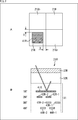
- FIG. 2A shows a planar configuration example of four pixels 21 (pixel 21R, pixel 21Gr, pixel 21Gb, and pixel 21B) arranged in a 2 ⁇ 2 manner according to the Bayer array.
- B shows a cross-sectional configuration example of the pixel 21R.
- the pixels 21R that receive red light and the pixels 21B that receive blue light are arranged in different rows and columns. Then, pixels 21Gr that receive green light are alternately arranged in the rows of the pixels 21R, and pixels 21Gb that receive green light are alternately arranged in the rows of the pixels 21B. Accordingly, as illustrated, the pixel 21R, the pixel 21Gr disposed on the right side of the pixel 21R, the pixel 21Gb disposed on the upper side of the pixel 21R, and the pixel 21B disposed on a diagonal position with respect to the pixel 21R. Are used as a set.
- the pixel 21R is configured by laminating a wiring layer 31, a light receiving unit 32R, and a red filter 33R in order from the lower side.
- the wiring layer 31 is configured by stacking a plurality of wirings insulated by an interlayer insulating film.
- the wiring layer 31 is configured by stacking four layers of wiring 41R to 44R. That is, the wiring layer 31 includes, in order from the light receiving unit 32R side, the wiring 41R serving as the first layer (1MT), the wirings 42R-1 and 42R-2 serving as the second layer (2MT), and the third layer (3MT). Wirings 44R-1 and 44R-2 to be the fourth layer (4MT) are formed.
- the light receiving unit 32R is a photodiode formed by a PN junction of a P-type region and an N-type region formed on a semiconductor substrate, receives red light transmitted through the red filter 33R, and charges according to the amount of light. Is generated and held.
- the red filter 33R is a color filter that transmits red light, and is disposed at a position corresponding to the pixel 21R. Although not shown, a color filter that transmits blue light is disposed in the pixel 21B, and a color filter that transmits green light is disposed in the pixels 21Gr and 21Gb.
- the wiring 41 ⁇ / b> R that is formed closest to the light receiving unit 32 ⁇ / b> R has symmetry with respect to the center (the shape or the optical center) of the pixel 21 ⁇ / b> R when the pixel 21 ⁇ / b> R is viewed in plan. It is formed in a square having a shape, and is arranged at the center of the pixel 21R. Thereby, in the pixel 21R, the asymmetry of the wirings 42R to 44R formed in the second layer or less (the side farther from the light receiving portion 32R) of the wiring layer 31 can be hidden by the wiring 41R, and the shading shape of the wiring 41R is reduced. Improvements can be made.
- the light transmitted through the light receiving portion 32 ⁇ / b> R is reflected by the wires 41 ⁇ / b> R to 44 ⁇ / b> R of the wiring layer 31 in the pixel 21 ⁇ / b> R because light on the long wavelength side is easily transmitted through the semiconductor substrate.
- the reflected light may enter the light receiving unit 32R. Therefore, when the wirings 41R to 44R are not formed symmetrically with respect to the pixel 21R, the amount of reflected light incident on the light receiving unit 32R is not constant depending on the incident angle of light due to the asymmetry. was there.
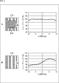
- FIG. 3A shows a simulation result of the pixel 21R having the configuration in which the wiring 41R having a shape having symmetry is provided
- FIG. 2B shows a wiring 41R having a shape having symmetry.
- the simulation result of the pixel 21R ′ having a configuration not provided is shown.
- the wiring 41R as described above with reference to FIG. 2 is formed in the first layer of the wiring layer 31, and the wirings 42R to 44R are formed asymmetrically in the second and lower layers of the wiring layer 31.
- the wirings 42 ⁇ / b> R to 44 ⁇ / b> R are formed asymmetrically in the second and lower layers of the wiring layer 31. That is, the simulation is performed with the pixel 21R and the pixel 21R ′ having different structures only in the presence or absence of the wiring 41R and the wirings 42R to 44R in the second and lower layers of the wiring layer 31 as a common structure.
- the horizontal axis indicates the incident angle of light incident on the pixel 21R and the pixel 21R ′ (when the angle orthogonal to the surface is 0 degree). Angle).
- the vertical axis indicates the ratio of the pixel signal for each incident angle with respect to the maximum value of the pixel signal, which is 100% (hereinafter referred to as shading).
- the shading with respect to the incident angle of light is substantially constant, and the pixel signal output from the pixel 21R is large regardless of the incident angle of light incident on the pixel 21R. It is shown that no change occurs (the change is very small).
- shading with respect to the incident angle of light is not constant, and its waveform (hereinafter referred to as a shading shape) is asymmetric. That is, it is shown that a large change occurs in the pixel signal output from the pixel 21R ′ according to the incident angle of the light incident on the pixel 21R ′.
- the shading shape deteriorates (on the positive side of the incident angle The difference in reflected light from the minus side increases).
- the pixel 21R can eliminate the adverse effects due to the asymmetry of the wirings 42R to 44R formed in the second and lower layers of the wiring layer 31 by providing the wiring 41R having a symmetrical shape in the center. Compared with the pixel 21R ′, the shading shape can be improved.
- the wiring 41R is formed so as to have an interval X between the adjacent pixels 21Gr and 21Gb.
- an interval X it is possible to prevent light incident on the pixel 21R from being reflected by the wiring 41R and entering the pixel 21Gr or 21Gb.
- the wiring 41R is formed so as to cover the entire surface of the first layer of the wiring layer 31 (all regions except the part where the through electrode is formed), the wiring formed in the second layer or lower It is considered that adverse effects due to the asymmetry of 42R to 44R can be avoided. However, when the wiring 41R is formed so as to cover the entire surface, there is a concern that light reflected by the wiring 41R may be mixed into the adjacent pixels 21Gr or 21Gb.
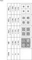
- FIG. 4 shows an output ratio (GR / GR) that is a ratio of the pixel signal GR output from the pixel 21Gr to the pixel signal GB output from the pixel 21Gb when the incident angle of light is changed in the row direction of the pixel 21R.
- the simulation results for determining GB) are shown.
- the incident angle is 0 degree (perpendicular to the sensor surface).
- the output ratio is 0.68%.
- the output ratio when the incident angle is 10 degrees is 2.08%, and the output ratio when the incident angle is 20 degrees is 15.96%. That is, as the incident angle of the light in the row direction of the pixel 21R increases, the mixing into the pixel 21Gr that is separated from and adjacent to the row direction is significantly increased as compared to the mixing into the pixel 21Gb adjacent in the column direction. It is shown.
- the output ratio when the incident angle is 0 degree is 0.41%, and the output ratio when the incident angle is 10 degrees is 2.13%.
- the output ratio when the incident angle is 20 degrees is 11.01%.
- the output ratio when the incident angle is 0 degree is 0.24%, and the output ratio when the incident angle is 10 degrees is 4.99%.
- the output ratio when the incident angle is 20 degrees is 12.31%.
- the output ratio when the incident angle is 0 degree is 1.60%
- the output ratio when the incident angle is 10 degrees is 4.34%.
- the output ratio when the incident angle is 20 degrees is 7.47%.
- the pixel 21R having the configuration in which the wiring 41R is formed so as to provide the space X between the pixels 21Gr and 21Gb has a configuration in which the wiring 41R is formed on the entire surface of the first layer of the wiring layer 31. Mixing of light into the pixels 21Gr and 21Gb can be suppressed. In particular, when the incident angle is large, the formation of the wiring 41R on the entire surface of the first layer of the wiring layer 31 causes a very large amount of light to be mixed. Mixing can be effectively suppressed.
- the pixel 21R by forming the wiring 41R with an interval X, the light passing through the gap is reflected by the wiring below the wiring 41R and mixed into the adjacent pixel 21Gr or 21Gb. Concerned. Therefore, a wiring for shielding such light can be provided in the first layer of the wiring layer 31 of the pixel 21Gr or 21Gb.
- a wiring for shielding such light can be provided in the first layer of the wiring layer 31 of the pixel 21Gr or 21Gb.
- the pixel 21G when it is not necessary to distinguish the pixels 21Gr and 21Gb from time to time, they are simply referred to as the pixel 21G.
- the light shielding wiring 41G provided in the pixel 21G will be described.
- FIG. 5 shows a cross-sectional configuration example of the pixel 21R and the pixel 21G.
- the pixel 21G is configured by stacking a light receiving unit 32G that receives green light and a green filter 33G that transmits green light on the wiring layer 31 in the same manner as the pixel 21R. .
- the wiring 41G formed with a predetermined width from the boundary with the pixel 21R is provided in the first layer of the wiring layer 31. Accordingly, the pixel 21G blocks light reflected by the second and lower wirings 42R to 44R provided in the wiring layer 31 of the pixel 21R by the wiring 41G, and prevents such light from entering the light receiving unit 32G. And the occurrence of color mixing can be reduced.
- the pixel 21R is provided with the wiring 41R formed symmetrically with respect to the center of the pixel 21R, so that the shading shape can be improved, and the pixel 21G is replaced by the pixel 21R.
- the wiring 41G for shielding the light reflected by the wiring layer 31, it is possible to prevent light from being mixed from the pixel 21R.
- the wiring 41R provided in the pixel 21R is also referred to as a symmetric wiring 41R
- the wiring 41G provided in the pixel 21G is also referred to as a light shielding wiring 41G.
- the symmetrical wiring 41R and the light shielding wiring 41G are connected to the drain power supply VDD.
- the distance between the symmetric wiring 41R and the light shielding wiring 41G and the width of the light shielding wiring 41G satisfy the conditions described below. It is preferable to satisfy.
- the light incident at the incident angle ⁇ is symmetrical so as to be reflected at the pixel 21G side end of the wiring 41R and enter the light receiving unit 32G.
- a distance Wr between the wiring 41R and the light shielding wiring 41G is set. That is, the distance Wr between the symmetric wiring 41R and the light shielding wiring 41G is the following with respect to the vertical distance Z1 between the light receiving unit 32R and the symmetric wiring 41R and the incident angle ⁇ at which light enters the pixel 21R. It is necessary to satisfy the relationship of Formula (1).
- the distance Wr is set to be larger than the lower limit (2 ⁇ Z1 ⁇ tan ⁇ ) represented by the expression (1) using the distance Z1 and the incident angle ⁇ , and is reflected by the symmetric wiring 41R of the pixel 21R. Light can be prevented from entering the light receiving unit 32G.
- the light reflected by the wiring is between the symmetric wiring 41R and the light shielding wiring 41G. It is necessary to prevent the light from entering the light receiving unit 32G.
- the pixel 21R shown in FIG. 7 has a configuration in which a wiring 43R-1 that is not covered by the symmetrical wiring 41R is provided. Then, for example, as indicated by the white arrow in FIG. 7, the light incident at the incident angle ⁇ passes through the gap between the symmetric wiring 41R and the light shielding wiring 41G, is reflected by the wiring 43R-1, and passes through the gap. Thus, it is necessary to prevent the light from entering the light receiving unit 32G.
- the distance Wr between the symmetric wiring 41R and the light shielding wiring 41G is the vertical distance Z2 between the symmetric wiring 41R and the wiring 43R-1 and the incident angle ⁇ at which light is incident on the pixel 21R. It is necessary to satisfy the relationship of the following formula (2).
- the distance Wr is covered with the symmetric wiring 41R of the pixel 21R. It is possible to avoid the light reflected by the wiring 43R-1 not entering the light receiving part 32G.
- the light reflected by the wiring is inside the pixel 21G rather than the light shielding wiring 41G. It is necessary to prevent the light from entering the light receiving unit 32G.
- the pixel 21R shown in FIG. 8 has a configuration in which a wiring 43R-1 that is not covered by the symmetrical wiring 41R is provided.
- a wiring 43R-1 that is not covered by the symmetrical wiring 41R is provided.
- the light incident at the incident angle ⁇ passes through the gap between the symmetrical wiring 41R and the light shielding wiring 41G and is reflected by the wiring 43R-1, and is reflected by the light shielding wiring 41G. It is also necessary to prevent the light from passing through the inside of the pixel 21G and entering the light receiving unit 32G.
- the width Wg of the light shielding wiring 41G is expressed by the following equation (3) with respect to the vertical distance Z2 between the symmetric wiring 41R and the wiring 43R-1 and the incident angle ⁇ at which light enters the pixel 21R. It is necessary to satisfy the relationship.
- the width Wg is not covered with the symmetrical wiring 41R of the pixel 21R.
- the light reflected by the wiring 43R-1 can be prevented from entering the light receiving unit 32G.
- the imaging device 11 can eliminate the asymmetry of the amount of received light according to the incident angle of the light incident on the pixel 21R.
- the wirings 42R to 44R formed in the second and lower layers of the wiring layer 31 may be formed asymmetrically, and the degree of freedom in designing the wiring layout can be increased.
- the number of signal lines, control lines, and the like can be increased to speed up reading of pixel signals.
- the incident angle ⁇ of light incident on the pixel 21 varies depending on the position where the pixel 21 is arranged in the pixel region 12. That is, the incident angle ⁇ is small in the central portion of the pixel region 12, and the incident angle ⁇ is large in the peripheral portion of the pixel region 12. Therefore, in the image sensor 11, it is preferable to correct the distance Wr and the width Wg according to the position of the pixel 21 (hereinafter referred to as pupil correction).
- FIG. 9A shows a cross-sectional configuration example of the pixel 21R and the pixel 21G arranged in the central portion of the pixel region 12, and FIG. 9B shows a configuration example arranged in the peripheral portion of the pixel region 12.
- FIG. 9B shows a configuration example arranged in the peripheral portion of the pixel region 12.
- a cross-sectional configuration example of the pixel 21R and the pixel 21G is shown.
- the incident angle ⁇ ⁇ b> 1 is small in the central portion of the pixel region 12, and the incident angle ⁇ ⁇ b> 2 is large in the peripheral portion of the pixel region 12. Accordingly, pupil correction is performed such that the distance Wr2 of the pixel 21R disposed in the peripheral portion of the pixel region 12 is larger than the distance Wr1 of the pixel 21R disposed in the central portion of the pixel region 12 (Wr1 ⁇ Wr2). Is preferred. Thereby, mixing of light from the pixel 21R to the pixel 21G can be appropriately reduced according to the position where the pixel 21R and the pixel 21G are arranged in the pixel region 12.
- FIG. 10A shows a cross-sectional configuration example of the pixel 21R and the pixel 21G disposed in the central portion of the pixel region 12, and FIG. 10B shows a peripheral portion of the pixel region 12.
- FIG. 10B shows a peripheral portion of the pixel region 12.
- a cross-sectional configuration example of the arranged pixel 21R and pixel 21G is shown.
- the incident angle ⁇ ⁇ b> 1 is small in the central portion of the pixel region 12, and the incident angle ⁇ ⁇ b> 2 is large in the peripheral portion of the pixel region 12. Therefore, the width Wg2 of the light shielding wiring 41G of the pixel 21G disposed in the peripheral portion of the pixel region 12 is larger than the width Wg1 of the light shielding wiring 41G of the pixel 21G disposed in the center of the pixel region 12 (Wg1 ⁇ Wg2). It is preferable to perform such pupil correction. Thereby, mixing of light from the pixel 21R to the pixel 21G can be appropriately reduced according to the position where the pixel 21R and the pixel 21G are arranged in the pixel region 12.
- the image sensor 11 can reduce color mixing regardless of the image height, and can capture an image in which noise due to color mixing is suppressed.
- the planar shape of the wiring 41R formed in the first layer of the wiring layer 31 is formed in a square, but the planar shape of the wiring 41R is limited to a square. There is nothing. Further, a wiring having a shape having symmetry may be formed in a layer other than the first layer of the wiring layer 31.
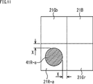
- the planar shape of the wiring 41R-a formed in the first layer of the wiring layer 31 is circular.
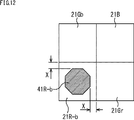
- the planar shape of the wiring 41R-b formed in the first layer of the wiring layer 31 is an octagon.
- the planar shape of the wiring 41R may be any shape as long as it is symmetric with respect to the center of the pixel 21R, and hides the asymmetry of the wiring in the second and lower layers. It is sufficient if the shading shape can be improved.
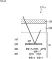
- the pixel 21R-c shown in FIG. 13 has a configuration in which a wiring 42R having symmetry is formed in the second layer of the wiring layer 31.
- the wiring 42R is formed in the second layer, but in the pixel 21R-c, since the wiring is not formed in the first layer of the wiring layer 31, the wiring 42R is formed closest to the light receiving portion 32R. Wiring is done.
- the wiring 42 ⁇ / b> R having symmetry may be provided in the second layer of the wiring layer 31. With such a configuration, the influence of the asymmetrical wiring 43R or 44R formed below the wiring 42R can be suppressed.
- the wiring 42R having symmetry is provided in the second layer of the wiring layer 31, and in the pixel 21G, the light shielding wiring 41G is provided in the first layer of the wiring layer 31, whereby the wiring 42R. It is possible to more reliably suppress the light reflected by the light and the light reflected by the wiring below the wiring 42R from entering the light receiving unit 32G.
- the configuration in which the symmetrical wiring 42R is provided in the pixel 21R in the first layer of the wiring layer 31 has been described.
- a wiring having symmetry may be provided in the layer.
- the provision of the symmetrical wiring 42R in the first layer of the wiring layer 31 is not limited to the pixel 21R, and may be, for example, the pixel 21 that receives infrared light.
- the pixel 21 that receives light having a wavelength of 620 nm or more a favorable effect can be obtained by providing a wiring having symmetry in the first layer of the wiring layer 31.
- the image pickup device 11 includes various image pickup systems such as a digital still camera and a digital video camera, a mobile phone having an image pickup function, and other devices having an image pickup function. It can be applied to electronic equipment.
- FIG. 14 is a block diagram illustrating a configuration example of an imaging device mounted on an electronic device.
- the imaging apparatus 101 includes an optical system 102, an imaging element 103, a signal processing circuit 104, a monitor 105, and a memory 106, and can capture still images and moving images.
- the optical system 102 includes one or more lenses, guides image light (incident light) from a subject to the image sensor 103, and forms an image on a light receiving surface (sensor unit) of the image sensor 103.
- the image sensor 11 of the above-described embodiment is applied.
- the image sensor 103 electrons are accumulated for a certain period according to an image formed on the light receiving surface via the optical system 102. Then, a signal corresponding to the electrons accumulated in the image sensor 103 is supplied to the signal processing circuit 104.
- the signal processing circuit 104 performs various signal processing on the pixel signal output from the image sensor 103.
- An image (image data) obtained by performing signal processing by the signal processing circuit 104 is supplied to the monitor 105 and displayed, or supplied to the memory 106 and stored (recorded).
- the imaging apparatus 101 configured as described above, by applying the imaging element 11 according to the above-described embodiment, for example, it is possible to capture a high-quality image that excludes adverse effects due to the incident angle of light.
- FIG. 15 is a diagram illustrating a usage example in which the above-described imaging element 11 (image sensor) is used.
- the image sensor described above can be used in various cases for sensing light such as visible light, infrared light, ultraviolet light, and X-ray as follows.
- Devices for taking images for viewing such as digital cameras and mobile devices with camera functions
- Devices used for traffic such as in-vehicle sensors that capture the back, surroundings, and interiors of vehicles, surveillance cameras that monitor traveling vehicles and roads, and ranging sensors that measure distances between vehicles, etc.
- Equipment used for home appliances such as TVs, refrigerators, air conditioners, etc. to take pictures and operate the equipment according to the gestures ⁇ Endoscopes, equipment that performs blood vessel photography by receiving infrared light, etc.
- Equipment used for medical and health care ⁇ Security equipment such as security surveillance cameras and personal authentication cameras ⁇ Skin measuring instrument for photographing skin and scalp photography Such as a microscope to do beauty Equipment used for sports-Equipment used for sports such as action cameras and wearable cameras for sports applications-Used for agriculture such as cameras for monitoring the condition of fields and crops apparatus
- this technique can also take the following structures.
- the said symmetrical wiring is arrange
- the solid-state image sensor as described in said (1).
- a light shielding wiring having a predetermined width from the boundary of the first pixel is provided in a layer closest to the light receiving unit (3)
- a predetermined distance provided between the second pixel and the symmetric wiring is corrected in accordance with an arrangement position of the first pixel.
- An electronic apparatus comprising a solid-state imaging device, wherein the pixel has a symmetric wiring formed in a symmetric shape with respect to the center of the pixel when the pixel is viewed in plan.
Landscapes
- Engineering & Computer Science (AREA)
- Multimedia (AREA)
- Signal Processing (AREA)
- Physics & Mathematics (AREA)
- Spectroscopy & Molecular Physics (AREA)
- Solid State Image Pick-Up Elements (AREA)
- Transforming Light Signals Into Electric Signals (AREA)
- Internal Circuitry In Semiconductor Integrated Circuit Devices (AREA)
Abstract
本開示は、画素に入射する光の入射角に応じた受光量の非対称性を解消することができるようにする固体撮像素子および電子機器に関する。 固体撮像素子は、半導体基板の裏面側から入射する光を受光する受光部を有する画素と、半導体基板の表面に積層される配線層とを備える。そして、画素は、平面視したときに、画素の中心に対して対称的な形状に形成される対称配線を有し、その対称配線は、配線層に形成される複数層の配線のうち、受光部の最も近くの層に配置される。本技術は、例えば、裏面照射型の固体撮像素子に適用できる。
Description
本開示は、固体撮像素子および電子機器に関し、特に、画素に入射する光の入射角に応じた受光量の非対称性を解消することができるようにした固体撮像素子および電子機器に関する。
従来、デジタルスチルカメラやデジタルビデオカメラなどの撮像機能を備えた電子機器においては、例えば、CCD(Charge Coupled Device)やCMOS(Complementary Metal Oxide Semiconductor)イメージセンサなどの固体撮像素子が使用されている。固体撮像素子は、光電変換を行うフォトダイオードと複数のトランジスタとが組み合わされた画素を有しており、被写体の像が結像する像面に配置された複数の画素から出力される画素信号に基づいて画像が構築される。
また、近年、フォトダイオードが形成される半導体基板を薄膜化して、半導体基板の表面に配線層を積層し、半導体基板の裏面側からフォトダイオードに光を入射する裏面照射型の固体撮像素子が多く利用されている。
ところで、裏面照射型の固体撮像素子では、裏面側から入射した光が半導体基板を透過して配線層に形成される配線で反射し、その反射光がフォトダイオードに入射することがある。このとき、配線層に形成される配線が、画素の中心に対して非対称な形状に形成されている場合、光の入射角に応じて、フォトダイオードに入射する反射光の光量が変化することがあった。つまり、この場合、一定の光量の光を、入射角を変えながら画素に入射しても、配線レイアウトの非対称性によってフォトダイオードに入射する反射光の光量が変化するため、画素の受光量が一定にはならないことがあった。
また、特許文献1には、半導体基板を透過しやすい長波長の光を受光する画素の下方に、配線が配置されないような配線レイアウトを採用し、配線層における光の反射を低減することで、光の混入を抑制させた裏面照射型の固体撮像素子が開示されている。
ところで、近年、画素から画素信号を読み出す速度の高速化に伴い、信号線や制御線が増加する傾向があり、上述の特許文献1のように、画素の下方に配線が配置されないような配線レイアウトを採用することは困難になっている。また、このような配線レイアウトは設計自由度が低いため、より設計自由度が高く、かつ、画素の受光量が光の入射角に対して一定となるようにすることが求められている。
本開示は、このような状況に鑑みてなされたものであり、画素に入射する光の入射角に応じた受光量の非対称性を解消することができるようにするものである。
本開示の一側面の固体撮像素子は、半導体基板の裏面側から入射する光を受光する受光部を有する画素と、前記半導体基板の表面に積層される配線層とを備え、前記画素は、前記画素を平面視したときに、前記画素の中心に対して対称的な形状に形成される対称配線を有する。
本開示の一側面の電子機器は、半導体基板の裏面側から入射する光を受光する受光部を有する画素と、前記半導体基板の表面に積層される配線層とを備え、前記画素は、前記画素を平面視したときに、前記画素の中心に対して対称的な形状に形成される対称配線を有する固体撮像素子を備える。
本開示の一側面においては、半導体基板の裏面側から入射する光を受光する受光部を有する画素と、半導体基板の表面に積層される配線層とを備え、画素には、画素を平面視したときに、画素の中心に対して対称的な形状の対称配線が形成される。
本開示の一側面によれば、画素に入射する光の入射角に応じた受光量の非対称性を解消することができる。
以下、本技術を適用した具体的な実施の形態について、図面を参照しながら詳細に説明する。
図1は、本技術を適用した撮像素子の一実施の形態の構成例を示すブロック図である。
図1に示すように、撮像素子11は、画素領域12、垂直駆動回路13、カラム信号処理回路14、水平駆動回路15、出力回路16、および制御回路17を備えて構成される。
画素領域12は、図示しない光学系により集光される光を受光する受光面である。画素領域12には、複数の画素21が行列状に配置されており、それぞれの画素21は、水平信号線22を介して行ごとに垂直駆動回路13に接続されるとともに、垂直信号線23を介して列ごとにカラム信号処理回路14に接続される。複数の画素21は、それぞれ受光する光の光量に応じたレベルの画素信号を出力し、それらの画素信号から、画素領域12に結像する被写体の画像が構築される。
垂直駆動回路13は、画素領域12に配置される複数の画素21の行ごとに順次、それぞれの画素21を駆動(転送や、選択、リセットなど)するための駆動信号を、水平信号線22を介して画素21に供給する。カラム信号処理回路14は、複数の画素21から垂直信号線23を介して出力される画素信号に対してCDS(Correlated Double Sampling:相関2重サンプリング)処理を施すことにより、画素信号のAD変換を行うとともにリセットノイズを除去する。
水平駆動回路15は、画素領域12に配置される複数の画素21の列ごとに順次、カラム信号処理回路14から画素信号をデータ出力信号線24に出力させるための駆動信号を、カラム信号処理回路14に供給する。出力回路16は、水平駆動回路15の駆動信号に従ったタイミングでカラム信号処理回路14からデータ出力信号線24を介して供給される画素信号を増幅し、後段の信号処理回路に出力する。制御回路17は、例えば、撮像素子11の各ブロックの駆動周期に従ったクロック信号を生成して供給することで、それらの各ブロックの駆動を制御する。
このように構成される撮像素子11では、例えば、赤色、緑色、および青色の光を透過するカラーフィルタが、いわゆるベイヤ配列に従って画素21ごとに配置されており、それぞれの画素21が各色の光の光量に応じた画素信号を出力する。また、撮像素子11は、画素21を構成するフォトダイオードが形成される半導体基板を薄膜化して、半導体基板の表面に配線層を積層し、半導体基板の裏面側から光を入射する裏面型の構造を採用することができる。
図2を参照して、画素21の構成について説明する。
図2のAには、ベイヤ配列に従って2×2で配置される4つの画素21(画素21R、画素21Gr、画素21Gb、および画素21B)の平面的な構成例が示されており、図2のBには、画素21Rの断面的な構成例が示されている。
図2のAに示すように、ベイヤ配列では、赤色の光を受光する画素21Rと青色の光を受光する画素21Bとが互いに異なる行および列に配置される。そして、画素21Rの行に画素21Rと交互に、緑色の光を受光する画素21Grが配置され、画素21Bの行に画素21Bと交互に、緑色の光を受光する画素21Gbが配置される。従って、図示するように、画素21Rと、画素21Rの右側に配置される画素21Grと、画素21Rの上側に配置される画素21Gbと、画素21Rに対して対角の位置に配置される画素21Bとが、一組として用いられる。
図2のBに示すように、画素21Rは、下側から順に、配線層31、受光部32R、および赤色フィルタ33Rが積層されて構成される。
配線層31は、層間絶縁膜により絶縁された複数の配線が積層されて構成されており、図2の例では、4層の配線41R乃至44Rが積層されて構成されている。即ち、配線層31には、受光部32R側から順に、1層目(1MT)となる配線41R、2層目(2MT)となる配線42R-1および42R-2、3層目(3MT)となる配線43R-1および43R-2、4層目(4MT)となる配線44R-1および44R-2が形成されている。
受光部32Rは、半導体基板に形成されるP型領域およびN型領域のPN接合によって構成されるフォトダイオードであり、赤色フィルタ33Rを透過する赤色の光を受光して、その光量に応じた電荷を発生して保持する。
赤色フィルタ33Rは、赤色の光を透過するカラーフィルタであり、画素21Rに対応する箇所に配置される。なお、図示しないが、画素21Bには、青色の光を透過するカラーフィルタが配置され、画素21Grおよび21Gbには、緑色の光を透過するカラーフィルタが配置されている。
そして、画素21Rでは、最も受光部32R側に形成される配線41Rが、画素21Rを平面的に見たときに、画素21Rの中心(形状的または光学的な中心)に対して対称性を備えた形状である正方形に形成され、画素21Rの中央に配置される。これにより、画素21Rでは、配線層31の2層目以下(受光部32Rより遠い側)に形成される配線42R乃至44Rの非対称性を、配線41Rによって隠すことができ、配線41Rのシェーディング形状の改善を図ることができる。
例えば、裏面型の撮像素子11では、特に、長波長側の光が半導体基板を透過しやすいことより、画素21Rにおいて、受光部32Rを透過した光が配線層31の配線41R乃至44Rで反射し、その反射光が受光部32Rに入射することがある。このため、配線41R乃至44Rが画素21Rに対して対称的な形状に形成されていない場合、その非対称性によって、受光部32Rに入射する反射光の光量が光の入射角によって一定とはならないことがあった。
図3を参照して、画素21Rに入射する光の入射角に応じた受光部32Rの受光量の非対称性の改善について説明する。
図3のAには、対称性を備えた形状の配線41Rが設けられた構成の画素21Rのシミュレーション結果が示されており、図2のBには、対称性を備えた形状の配線41Rが設けられていない構成の画素21R’のシミュレーション結果が示されている。
画素21Rでは、図2を参照して上述したような配線41Rが配線層31の1層目に形成されており、配線層31の2層目以下には配線42R乃至44Rが非対称に形成されている。一方、画素21R’では、配線層31の2層目以下に配線42R乃至44Rが非対称に形成されている。即ち、画素21Rおよび画素21R’は、配線41Rの有無だけを異なる構造とし、配線層31の2層目以下の配線42R乃至44Rを共通の構造として、シミュレーションが行われている。
また、図3のAおよび図3のBの右側に示すシミュレーション結果において、横軸は、画素21Rおよび画素21R’に入射する光の入射角(表面に対して直交する角度を0度としたときの角度)を示している。また、縦軸は、画素信号の最大値を100%とし、その最大値に対する入射角ごとの画素信号の比率(以下、シェーディングと称する)を示している。
図3のAに示すように、画素21Rでは、光の入射角に対するシェーディングがほぼ一定となっており、画素21Rに入射する光の入射角によらず、画素21Rから出力される画素信号に大きな変化が発生しない(変化が非常に小さい)ことが示されている。
これに対し、図3のBに示すように、画素21R’では、光の入射角に対するシェーディングが一定とはならず、その波形(以下、シェーディング形状と称する)が非対称となっている。つまり、画素21R’に入射する光の入射角に応じて、画素21R’から出力される画素信号に大きな変化が発生することが示されている。このように、画素21R’は、入射光の入射角が変化すると、配線42R乃至44Rの非対称性によって、画素21R’の受光量が変化し、即ち、シェーディング形状が悪化(入射角のプラス側とマイナス側との反射光の差分が増加)してしまう。
従って、画素21Rは、対称性を備えた形状の配線41Rを中央に設けることにより、配線層31の2層目以下に形成される配線42R乃至44Rの非対称性による悪影響を排除することができ、画素21R’と比較してシェーディング形状を改善することができる。
ここで、図2のAに示すように、画素21Rにおいて、配線41Rは、隣接する画素21Grおよび21Gbとの間にそれぞれ間隔Xが設けられるように形成される。このような間隔Xを設けることにより、画素21Rに入射した光が配線41Rで反射して画素21Grまたは21Gbに混入することを回避することができる。
例えば、配線層31の1層目の全面(貫通電極が形成される部分を除く全ての領域)を覆うように配線41Rを形成する構成を採用することで、2層目以下に形成される配線42R乃至44Rの非対称性による悪影響を回避することができると考えられる。しかしながら、全面を覆うように配線41Rを形成した場合には、配線41Rで反射した光が、隣接する画素21Grまたは21Gbに混入することが懸念される。
ここで、図4を参照して、配線41Rと画素21Grおよび21Gbとの間に設けられる間隔Xと、画素21Rから画素21Grまたは21Gbへの光の混入との関係について説明する。
図4には、画素21Rの行方向に光の入射角を変えたときにおいて、画素21Gbから出力される画素信号GBに対する、画素21Grから出力される画素信号GRの比率である出力比率(GR/GB)を求めたシミュレーション結果が示されている。
例えば、配線41Rの間隔Xを0nmに設定した場合、即ち、配線層31の1層目の全面に配線41Rを形成した場合、入射角が0度(センサ面に対して直交)であるときの出力比率は0.68%である。また、入射角が10度であるときの出力比率は2.08%であり、入射角が20度であるときの出力比率は15.96%である。即ち、画素21Rの行方向への光の入射角が増加するのに伴って、行方向に離接する画素21Grへの混入が、列方向に隣接する画素21Gbへの混入よりも大幅に増加することが示されている。
また、配線41Rの間隔Xを300nmに設定した場合には、入射角が0度であるときの出力比率は0.41%であり、入射角が10度であるときの出力比率は2.13%であり、入射角が20度であるときの出力比率は11.01%である。また、配線41Rの間隔Xを600nmに設定した場合には、入射角が0度であるときの出力比率は0.24%であり、入射角が10度であるときの出力比率は4.99%であり、入射角が20度であるときの出力比率は12.31%である。また、配線41Rの間隔Xを900nmに設定した場合には、入射角が0度であるときの出力比率は-1.60%であり、入射角が10度であるときの出力比率は4.34%であり、入射角が20度であるときの出力比率は7.47%である。
このように、画素21Grおよび21Gbとの間に間隔Xを設けるように配線41Rを形成する構成の画素21Rは、配線層31の1層目の全面に配線41Rを形成する構成と比較して、画素21Grおよび21Gbへの光の混入を抑制することができる。特に、入射角が大きい場合において、配線層31の1層目の全面に配線41Rを形成することによって、光の混入が非常に大きくなってしまうのに対し、間隔Xを設けることによって、光の混入を効果的に抑制することができる。
従って、このような光の混入を抑制するために、画素21Rでは、適切な間隔Xを設けて配線41Rをレイアウトする必要がある。
ところで、画素21Rにおいて、間隔Xを設けて配線41Rを形成することによって、その隙間を通過した光が配線41Rよりも下側の配線で反射して、隣接する画素21Grまたは21Gbに混入することが懸念される。そこで、画素21Grまたは21Gbの配線層31の1層目に、そのような光を遮光するための配線を設けることができる。なお、以下適宜、画素21Grおよび21Gbを区別する必要がない場合、単に、画素21Gと称する。
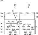
図5を参照して、画素21Gに設けられる遮光用の配線41Gについて説明する。
図5には、画素21Rおよび画素21Gの断面的な構成例が示されている。図5に示すように、画素21Gは、画素21Rと同様に、配線層31に対し、緑色の光を受光する受光部32Gと、緑色の光を透過する緑色フィルタ33Gが積層されて構成される。
そして、画素21Gでは、配線層31の1層目に、画素21Rとの境界から所定の幅を有して形成された配線41Gが設けられる。従って、画素21Gは、配線41Gにより、画素21Rの配線層31に設けられる2層目以下の配線42R乃至44Rにおいて反射する光を遮光し、そのような光が受光部32Gに入射することを防止することができ、混色の発生を低減することができる。
以上のように、撮像素子11では、画素21Rが、画素21Rの中心に対して対称に形成された配線41Rを設けることで、シェーディング形状の改善を図ることができるとともに、画素21Gが、画素21Rの配線層31で反射する光を遮光するための配線41Gを設けることで、画素21Rからの光の混入を防止することができる。
ここで、以下適宜、画素21Rに設けられる配線41Rを対称配線41Rとも称し、画素21Gに設けられる配線41Gを遮光配線41Gとも称する。例えば、対称配線41Rと遮光配線41Gは、ドレイン電源VDDに接続される。
そして、撮像素子11では、画素21Rから画素21Gへの光の混入を防止するために、対称配線41Rと遮光配線41Gと間の距離、および、遮光配線41Gの幅が、以下で説明する条件を満たすことが好ましい。
例えば、画素21Rにおいて、対称配線41Rで反射した光が、受光部32Gに入射することを防止する必要がある。
図6を参照して、対称配線41Rと遮光配線41Gと間の距離が満たす第1の条件について説明する。
例えば、図6において白抜きの矢印で示すように、入射角θで入射した光が、配線41Rの画素21G側の端部で反射して受光部32Gに入射することを回避するように、対称配線41Rと遮光配線41Gとの間の距離Wrが設定される。即ち、対称配線41Rと遮光配線41Gとの間の距離Wrは、受光部32Rと対称配線41Rとの垂直方向の距離Z1、および、光が画素21Rに入射する入射角θに対して、次の式(1)の関係を満たす必要がある。

このように、距離Wrを、距離Z1および入射角θを用いた式(1)で示される下限値(2×Z1×tanθ)よりも大きく設定することで、画素21Rの対称配線41Rで反射した光が、受光部32Gに入射することを回避することができる。
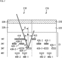
次に、画素21Rにおいて、対称配線41Rにより覆われていない配線が、配線層31の2層目以下に設けられているとき、その配線で反射する光が、対称配線41Rと遮光配線41Gとの間を通過して、受光部32Gに入射することを防止する必要がある。
図7を参照して、対称配線41Rと遮光配線41Gとの距離が満たす第2の条件について説明する。
図7に示す画素21Rは、対称配線41Rにより覆われていない配線43R-1が設けられた構成となっている。そして、例えば、図7において白抜きの矢印で示すように、入射角θで入射した光が、対称配線41Rおよび遮光配線41Gの隙間を通過して配線43R-1で反射し、その隙間を通過して受光部32Gに入射することを防止する必要がある。
このため、対称配線41Rと遮光配線41Gとの間の距離Wrは、対称配線41Rと配線43R-1との垂直方向の距離Z2、および、光が画素21Rに入射する入射角θに対して、次の式(2)の関係を満たす必要がある。

このように、距離Wrを、距離Z2および入射角θを用いた式(2)で示される上限値(2×Z2×tanθ)よりも小さく設定することで、画素21Rの対称配線41Rで覆われていない配線43R-1で反射した光が、受光部32Gに入射することを回避することができる。
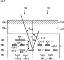
次に、画素21Rにおいて、対称配線41Rにより覆われていない配線が、配線層31の2層目以下に設けられているとき、その配線で反射する光が、遮光配線41Gよりも画素21Gの内側を通過して、受光部32Gに入射することを防止する必要がある。
図8を参照して、遮光配線41Gの幅が満たす条件について説明する。
図8に示す画素21Rは、対称配線41Rにより覆われていない配線43R-1が設けられた構成となっている。そして、例えば、図8において白抜きの矢印で示すように、入射角θで入射した光が、対称配線41Rおよび遮光配線41Gの隙間を通過して配線43R-1で反射し、遮光配線41Gよりも画素21Gの内側を通過して、受光部32Gに入射することを防止する必要がある。
このため、遮光配線41Gの幅Wgは、対称配線41Rと配線43R-1との垂直方向の距離Z2、および、光が画素21Rに入射する入射角θに対して、次の式(3)の関係を満たす必要がある。

このように、幅Wgを、距離Z2および入射角θを用いた式(3)で示される下限値(Z2×tanθ)よりも大きく設定することで、画素21Rの対称配線41Rで覆われていない配線43R-1で反射した光が、受光部32Gに入射することを回避することができる。
以上のように、撮像素子11は、画素21Rに入射する光の入射角に応じた受光量の非対称性を解消することができる。特に、画素21Rにおいて、配線層31の2層目以下に形成される配線42R乃至44Rを非対称に形成してもよく、配線レイアウトの設計自由度を高くすることができる。例えば、撮像素子11では、信号線や制御線などを増加させて、画素信号の読み出しを高速化させることができる。
ところで、撮像素子11において、画素21に入射する光の入射角θは、画素21が画素領域12において配置される位置によって異なるものとなる。即ち、画素領域12の中央部では、入射角θは小さくなり、画素領域12の周辺部では、入射角θは大きくなる。従って、撮像素子11では、画素21の位置に応じて距離Wrおよび幅Wgを補正(以下、瞳補正と称する)することが好ましい。
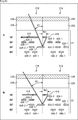
次に、図9および図10を参照して、画素21が配置される位置に応じた距離Wrおよび幅Wgの瞳補正について説明する。
図9のAには、画素領域12の中央部に配置される画素21Rおよび画素21Gの断面的な構成例が示されており、図9のBには、画素領域12の周辺部に配置される画素21Rおよび画素21Gの断面的な構成例が示されている。
図9に示すように、画素領域12の中央部では入射角θ1は小さく、画素領域12の周辺部では入射角θ2は大きくなる。従って、画素領域12の周辺部に配置される画素21Rの距離Wr2は、画素領域12の中央部に配置される画素21Rの距離Wr1よりも大きく(Wr1<Wr2)なるような瞳補正を行うことが好ましい。これにより、画素21Rおよび画素21Gが画素領域12において配置される位置に応じて適切に、画素21Rから画素21Gへの光の混入を低減することができる。
また、図10のAには、画素領域12の中央部に配置される画素21Rおよび画素21Gの断面的な構成例が示されており、図10のBには、画素領域12の周辺部に配置される画素21Rおよび画素21Gの断面的な構成例が示されている。
図10に示すように、画素領域12の中央部では入射角θ1は小さく、画素領域12の周辺部では入射角θ2は大きくなる。従って、画素領域12の周辺部に配置される画素21Gの遮光配線41Gの幅Wg2は、画素領域12の中央部に配置される画素21Gの遮光配線41Gの幅Wg1よりも大きく(Wg1<Wg2)なるような瞳補正を行うことが好ましい。これにより、画素21Rおよび画素21Gが画素領域12において配置される位置に応じて適切に、画素21Rから画素21Gへの光の混入を低減させることができる。
以上のような瞳補正を行うことで、撮像素子11は、像高によらず混色を低減することができ、混色によるノイズを抑制した画像を撮像することができる。
なお、図2に示す画素21Rでは、配線層31の1層目に形成される配線41Rの平面的な形状は正方形に形成されているが、配線41Rの平面的な形状は正方形に限定されることはない。また、対称性を備えた形状の配線が配線層31の1層目以外に形成されてもよい。
次に、図11乃至図13を参照して、画素21Rの変形例について説明する。
例えば、図11に示す画素21R-aでは、配線層31の1層目に形成される配線41R-aの平面的な形状は円形に形成されている。また、図12に示す画素21R-bでは、配線層31の1層目に形成される配線41R-bの平面的な形状は八角形に形成されている。このように、配線41Rの平面的な形状は、画素21Rの中心に対して対称となる形状であれば、どのような形状であってもよく、2層目以下の配線の非対称性を隠してシェーディング形状の改善を図ることができればよい。
また、図13に示す画素21R-cは、配線層31の2層目に対称性を備えた配線42Rが形成された構成となっている。なお、配線42Rは2層目に形成されているが、画素21R-cでは、配線層31の1層目には配線が形成されていないことより、配線42Rが、最も受光部32R側に形成された配線となっている。このように、配線層31における配線レイアウトに自由度がある場合には、対称性を備える配線42Rを配線層31の2層目に設けてもよい。このような構成によって、配線42Rにより、それ以下に形成される非対称な配線43Rまたは44Rの影響を抑制することができる。
また、例えば、画素21Rでは、配線層31の2層目に対称性を備えた配線42Rを設け、画素21Gでは、配線層31の1層目に遮光用の配線41Gを設けることによって、配線42Rで反射した光や、配線42R以下の配線で反射した光が、受光部32Gに入射することをより確実に抑制することができる。
なお、上述した本実施の形態では、配線層31の1層目に対称性を備えた配線42Rを画素21Rに設ける構成について説明したが、もちろん、画素21Bや画素21Gにおいて、配線層31の1層目に対称性を備えた配線を設ける構成としてもよい。このように、配線層31の1層目に対称性を備えた配線42Rを設けるのは、画素21Rに限定されることはなく、例えば、赤外光を受光する画素21であってもよい。例えば、波長が620nm以上である光を受光する画素21において、配線層31の1層目に対称性を備えた配線を設けることで、良好な効果を得ることができる。
なお、上述したような実施の形態の撮像素子11は、例えば、デジタルスチルカメラやデジタルビデオカメラなどの撮像システム、撮像機能を備えた携帯電話機、または、撮像機能を備えた他の機器といった各種の電子機器に適用することができる。
図14は、電子機器に搭載される撮像装置の構成例を示すブロック図である。
図14に示すように、撮像装置101は、光学系102、撮像素子103、信号処理回路104、モニタ105、およびメモリ106を備えて構成され、静止画像および動画像を撮像可能である。
光学系102は、1枚または複数枚のレンズを有して構成され、被写体からの像光(入射光)を撮像素子103に導き、撮像素子103の受光面(センサ部)に結像させる。
撮像素子103としては、上述した実施の形態の撮像素子11が適用される。撮像素子103には、光学系102を介して受光面に結像される像に応じて、一定期間、電子が蓄積される。そして、撮像素子103に蓄積された電子に応じた信号が信号処理回路104に供給される。
信号処理回路104は、撮像素子103から出力された画素信号に対して各種の信号処理を施す。信号処理回路104が信号処理を施すことにより得られた画像(画像データ)は、モニタ105に供給されて表示されたり、メモリ106に供給されて記憶(記録)されたりする。
このように構成されている撮像装置101では、上述した実施の形態の撮像素子11を適用することで、例えば、光の入射角による悪影響を排除した高画質な画像を撮像することができる。
図15は、上述の撮像素子11(イメージセンサ)を使用する使用例を示す図である。
上述したイメージセンサは、例えば、以下のように、可視光や、赤外光、紫外光、X線等の光をセンシングする様々なケースに使用することができる。
・ディジタルカメラや、カメラ機能付きの携帯機器等の、鑑賞の用に供される画像を撮影する装置
・自動停止等の安全運転や、運転者の状態の認識等のために、自動車の前方や後方、周囲、車内等を撮影する車載用センサ、走行車両や道路を監視する監視カメラ、車両間等の測距を行う測距センサ等の、交通の用に供される装置
・ユーザのジェスチャを撮影して、そのジェスチャに従った機器操作を行うために、TVや、冷蔵庫、エアーコンディショナ等の家電に供される装置
・内視鏡や、赤外光の受光による血管撮影を行う装置等の、医療やヘルスケアの用に供される装置
・防犯用途の監視カメラや、人物認証用途のカメラ等の、セキュリティの用に供される装置
・肌を撮影する肌測定器や、頭皮を撮影するマイクロスコープ等の、美容の用に供される装置
・スポーツ用途等向けのアクションカメラやウェアラブルカメラ等の、スポーツの用に供される装置
・畑や作物の状態を監視するためのカメラ等の、農業の用に供される装置
・自動停止等の安全運転や、運転者の状態の認識等のために、自動車の前方や後方、周囲、車内等を撮影する車載用センサ、走行車両や道路を監視する監視カメラ、車両間等の測距を行う測距センサ等の、交通の用に供される装置
・ユーザのジェスチャを撮影して、そのジェスチャに従った機器操作を行うために、TVや、冷蔵庫、エアーコンディショナ等の家電に供される装置
・内視鏡や、赤外光の受光による血管撮影を行う装置等の、医療やヘルスケアの用に供される装置
・防犯用途の監視カメラや、人物認証用途のカメラ等の、セキュリティの用に供される装置
・肌を撮影する肌測定器や、頭皮を撮影するマイクロスコープ等の、美容の用に供される装置
・スポーツ用途等向けのアクションカメラやウェアラブルカメラ等の、スポーツの用に供される装置
・畑や作物の状態を監視するためのカメラ等の、農業の用に供される装置
なお、本技術は以下のような構成も取ることができる。
(1)
半導体基板の裏面側から入射する光を受光する受光部を有する画素と、
前記半導体基板の表面に積層される配線層と
を備え、
前記画素は、前記画素を平面視したときに、前記画素の中心に対して対称的な形状に形成される対称配線を有する
固体撮像素子。
(2)
前記対称配線は、前記配線層に形成される複数層の配線のうち、前記受光部の最も近くの層に配置される
上記(1)に記載の固体撮像素子。
(3)
前記対称配線を有する第1の画素に対して隣接する第2の画素と、前記対称配線との間に所定距離の隙間が設けられる
上記(1)または(2)に記載の固体撮像素子。
(4)
前記第2の画素の前記配線層に形成される複数層の配線のうち、前記受光部の最も近くの層に、前記第1の画素の境界から所定幅の遮光配線が設けられる
上記(3)に記載の固体撮像素子。
(5)
前記第1の画素において、前記第2の画素と前記対称配線との間に設けられる所定距離は、前記第1の画素の配置位置に応じて補正される
上記(3)に記載の固体撮像素子。
(6)
前記第2の画素に設けられる前記遮光配線の所定幅は、前記第2の画素の配置位置に応じて補正される
上記(4)に記載の固体撮像素子。
(7)
前記第1の画素は、赤色の光を受光する画素であり、前記第2の画素は、緑色の光を受光する画素である
上記(1)から(6)までのいずれかに記載の固体撮像素子。
(8)
前記第1の画素は、波長が620nm以上である光を受光する画素である
上記(1)から(7)までのいずれかに記載の固体撮像素子。
(9)
半導体基板の裏面側から入射する光を受光する受光部を有する画素と、
前記半導体基板の表面に積層される配線層と
を備え、
前記画素は、前記画素を平面視したときに、前記画素の中心に対して対称的な形状に形成される対称配線を有する
固体撮像素子を備える電子機器。
(1)
半導体基板の裏面側から入射する光を受光する受光部を有する画素と、
前記半導体基板の表面に積層される配線層と
を備え、
前記画素は、前記画素を平面視したときに、前記画素の中心に対して対称的な形状に形成される対称配線を有する
固体撮像素子。
(2)
前記対称配線は、前記配線層に形成される複数層の配線のうち、前記受光部の最も近くの層に配置される
上記(1)に記載の固体撮像素子。
(3)
前記対称配線を有する第1の画素に対して隣接する第2の画素と、前記対称配線との間に所定距離の隙間が設けられる
上記(1)または(2)に記載の固体撮像素子。
(4)
前記第2の画素の前記配線層に形成される複数層の配線のうち、前記受光部の最も近くの層に、前記第1の画素の境界から所定幅の遮光配線が設けられる
上記(3)に記載の固体撮像素子。
(5)
前記第1の画素において、前記第2の画素と前記対称配線との間に設けられる所定距離は、前記第1の画素の配置位置に応じて補正される
上記(3)に記載の固体撮像素子。
(6)
前記第2の画素に設けられる前記遮光配線の所定幅は、前記第2の画素の配置位置に応じて補正される
上記(4)に記載の固体撮像素子。
(7)
前記第1の画素は、赤色の光を受光する画素であり、前記第2の画素は、緑色の光を受光する画素である
上記(1)から(6)までのいずれかに記載の固体撮像素子。
(8)
前記第1の画素は、波長が620nm以上である光を受光する画素である
上記(1)から(7)までのいずれかに記載の固体撮像素子。
(9)
半導体基板の裏面側から入射する光を受光する受光部を有する画素と、
前記半導体基板の表面に積層される配線層と
を備え、
前記画素は、前記画素を平面視したときに、前記画素の中心に対して対称的な形状に形成される対称配線を有する
固体撮像素子を備える電子機器。
なお、本実施の形態は、上述した実施の形態に限定されるものではなく、本開示の要旨を逸脱しない範囲において種々の変更が可能である。
11 撮像素子, 12 画素領域, 13 垂直駆動回路, 14 カラム信号処理回路, 15 水平駆動回路, 16 出力回路, 17 制御回路, 21 画素, 22 水平信号線, 23 垂直信号線, 24 データ出力信号線, 31 配線層, 32Rおよび32G 受光部, 33R 赤色フィルタ, 33G 緑色フィルタ, 41乃至44 配線
Claims (9)
- 半導体基板の裏面側から入射する光を受光する受光部を有する画素と、
前記半導体基板の表面に積層される配線層と
を備え、
前記画素は、前記画素を平面視したときに、前記画素の中心に対して対称的な形状に形成される対称配線を有する
固体撮像素子。 - 前記対称配線は、前記配線層に形成される複数層の配線のうち、前記受光部の最も近くの層に配置される
請求項1に記載の固体撮像素子。 - 前記対称配線を有する第1の画素に対して隣接する第2の画素と、前記対称配線との間に所定距離の隙間が設けられる
請求項1に記載の固体撮像素子。 - 前記第2の画素の前記配線層に形成される複数層の配線のうち、前記受光部の最も近くの層に、前記第1の画素の境界から所定幅の遮光配線が設けられる
請求項3に記載の固体撮像素子。 - 前記第1の画素において、前記第2の画素と前記対称配線との間に設けられる所定距離は、前記第1の画素の配置位置に応じて補正される
請求項3に記載の固体撮像素子。 - 前記第2の画素に設けられる前記遮光配線の所定幅は、前記第2の画素の配置位置に応じて補正される
請求項4に記載の固体撮像素子。 - 前記第1の画素は、赤色の光を受光する画素であり、前記第2の画素は、緑色の光を受光する画素である
請求項1に記載の固体撮像素子。 - 前記第1の画素は、波長が620nm以上である光を受光する画素である
請求項1に記載の固体撮像素子。 - 半導体基板の裏面側から入射する光を受光する受光部を有する画素と、
前記半導体基板の表面に積層される配線層と
を備え、
前記画素は、前記画素を平面視したときに、前記画素の中心に対して対称的な形状に形成される対称配線を有する
固体撮像素子を備える電子機器。
Priority Applications (2)
| Application Number | Priority Date | Filing Date | Title |
|---|---|---|---|
| CN201680017826.6A CN107431078B (zh) | 2015-04-07 | 2016-03-24 | 固体摄像元件和电子设备 |
| US15/562,758 US11004885B2 (en) | 2015-04-07 | 2016-03-24 | Solid-state image capture element and electronic device enabled to eliminate asymmetry of a light reception amount |
Applications Claiming Priority (2)
| Application Number | Priority Date | Filing Date | Title |
|---|---|---|---|
| JP2015-078600 | 2015-04-07 | ||
| JP2015078600A JP2016201397A (ja) | 2015-04-07 | 2015-04-07 | 固体撮像素子および電子機器 |
Publications (1)
| Publication Number | Publication Date |
|---|---|
| WO2016163242A1 true WO2016163242A1 (ja) | 2016-10-13 |
Family
ID=57071872
Family Applications (1)
| Application Number | Title | Priority Date | Filing Date |
|---|---|---|---|
| PCT/JP2016/059323 Ceased WO2016163242A1 (ja) | 2015-04-07 | 2016-03-24 | 固体撮像素子および電子機器 |
Country Status (4)
| Country | Link |
|---|---|
| US (1) | US11004885B2 (ja) |
| JP (1) | JP2016201397A (ja) |
| CN (1) | CN107431078B (ja) |
| WO (1) | WO2016163242A1 (ja) |
Families Citing this family (2)
| Publication number | Priority date | Publication date | Assignee | Title |
|---|---|---|---|---|
| CN113196488A (zh) | 2018-12-26 | 2021-07-30 | 索尼半导体解决方案公司 | 摄像元件和摄像装置 |
| JP7802005B2 (ja) * | 2020-09-25 | 2026-01-19 | ソニーセミコンダクタソリューションズ株式会社 | 固体撮像装置及び電子機器 |
Citations (3)
| Publication number | Priority date | Publication date | Assignee | Title |
|---|---|---|---|---|
| JP2013055159A (ja) * | 2011-09-01 | 2013-03-21 | Canon Inc | 固体撮像装置 |
| JP2014086699A (ja) * | 2012-10-26 | 2014-05-12 | Canon Inc | 固体撮像装置および撮像システム |
| JP2014096540A (ja) * | 2012-11-12 | 2014-05-22 | Canon Inc | 固体撮像装置およびその製造方法ならびにカメラ |
Family Cites Families (11)
| Publication number | Priority date | Publication date | Assignee | Title |
|---|---|---|---|---|
| JP3890333B2 (ja) * | 2004-02-06 | 2007-03-07 | キヤノン株式会社 | 固体撮像装置 |
| JP2010056167A (ja) * | 2008-08-26 | 2010-03-11 | Sony Corp | 固体撮像素子及びその製造方法 |
| US8889455B2 (en) * | 2009-12-08 | 2014-11-18 | Zena Technologies, Inc. | Manufacturing nanowire photo-detector grown on a back-side illuminated image sensor |
| KR101550866B1 (ko) * | 2009-02-09 | 2015-09-08 | 삼성전자주식회사 | 광학적 크로스토크를 개선하기 위하여, 절연막의 트렌치 상부만을 갭필하여 에어 갭을 형성하는 이미지 센서의 제조방법 |
| JP2011129627A (ja) * | 2009-12-16 | 2011-06-30 | Panasonic Corp | 半導体装置 |
| US8389921B2 (en) * | 2010-04-30 | 2013-03-05 | Omnivision Technologies, Inc. | Image sensor having array of pixels and metal reflectors with widths scaled based on distance from center of the array |
| JP2012049289A (ja) * | 2010-08-26 | 2012-03-08 | Sony Corp | 固体撮像装置とその製造方法、並びに電子機器 |
| US9373732B2 (en) * | 2012-02-07 | 2016-06-21 | Semiconductor Components Industries, Llc | Image sensors with reflective optical cavity pixels |
| JP2014086551A (ja) * | 2012-10-23 | 2014-05-12 | Canon Inc | 撮像装置及びカメラ |
| US9093345B2 (en) | 2012-10-26 | 2015-07-28 | Canon Kabushiki Kaisha | Solid-state imaging apparatus and imaging system |
| JP2015056417A (ja) * | 2013-09-10 | 2015-03-23 | ソニー株式会社 | 撮像装置、製造装置、製造方法、並びに電子機器 |
-
2015
- 2015-04-07 JP JP2015078600A patent/JP2016201397A/ja active Pending
-
2016
- 2016-03-24 WO PCT/JP2016/059323 patent/WO2016163242A1/ja not_active Ceased
- 2016-03-24 CN CN201680017826.6A patent/CN107431078B/zh not_active Expired - Fee Related
- 2016-03-24 US US15/562,758 patent/US11004885B2/en not_active Expired - Fee Related
Patent Citations (3)
| Publication number | Priority date | Publication date | Assignee | Title |
|---|---|---|---|---|
| JP2013055159A (ja) * | 2011-09-01 | 2013-03-21 | Canon Inc | 固体撮像装置 |
| JP2014086699A (ja) * | 2012-10-26 | 2014-05-12 | Canon Inc | 固体撮像装置および撮像システム |
| JP2014096540A (ja) * | 2012-11-12 | 2014-05-22 | Canon Inc | 固体撮像装置およびその製造方法ならびにカメラ |
Also Published As
| Publication number | Publication date |
|---|---|
| CN107431078B (zh) | 2021-11-16 |
| JP2016201397A (ja) | 2016-12-01 |
| US11004885B2 (en) | 2021-05-11 |
| CN107431078A (zh) | 2017-12-01 |
| US20180083059A1 (en) | 2018-03-22 |
Similar Documents
| Publication | Publication Date | Title |
|---|---|---|
| US10741605B2 (en) | Solid-state image sensor, imaging device, and electronic equipment | |
| US10425624B2 (en) | Solid-state image capturing device and electronic device | |
| US20180301491A1 (en) | Solid-state imaging device, manufacturing method thereof, and electronic device | |
| JP2015128131A (ja) | 固体撮像素子および電子機器 | |
| US20170358614A1 (en) | Solid-state imaging device and electronic apparatus | |
| CN107409184B (zh) | 固态成像元件、驱动方法以及电子设备 | |
| WO2017138370A1 (ja) | 固体撮像素子およびその製造方法、並びに電子機器 | |
| CN108352395B (zh) | 固态摄像装置和电子设备 | |
| JP2016127043A (ja) | 固体撮像素子及び電子機器 | |
| JP7005886B2 (ja) | 固体撮像素子、および電子機器 | |
| US12096642B2 (en) | Solid-state imaging device with organic photoelectric conversion film over photodiodes | |
| CN103152530A (zh) | 固体摄像装置和电子设备 | |
| TW202123441A (zh) | 成像裝置、生產方法及電子設備 | |
| US10032823B2 (en) | Solid-state imaging device and imaging apparatus | |
| JPWO2016136488A1 (ja) | 半導体装置、固体撮像素子、撮像装置、並びに電子機器 | |
| WO2016051594A1 (ja) | 固体撮像装置および撮像装置 | |
| CN107431078B (zh) | 固体摄像元件和电子设备 | |
| JP2015159231A (ja) | 固体撮像装置 | |
| JP2014103596A (ja) | 撮像素子、及び撮像装置 |
Legal Events
| Date | Code | Title | Description |
|---|---|---|---|
| 121 | Ep: the epo has been informed by wipo that ep was designated in this application |
Ref document number: 16776410 Country of ref document: EP Kind code of ref document: A1 |
|
| WWE | Wipo information: entry into national phase |
Ref document number: 15562758 Country of ref document: US |
|
| NENP | Non-entry into the national phase |
Ref country code: DE |
|
| 122 | Ep: pct application non-entry in european phase |
Ref document number: 16776410 Country of ref document: EP Kind code of ref document: A1 |