WO2016159315A1 - 合金材料、コンタクトプローブおよび接続端子 - Google Patents
合金材料、コンタクトプローブおよび接続端子 Download PDFInfo
- Publication number
- WO2016159315A1 WO2016159315A1 PCT/JP2016/060829 JP2016060829W WO2016159315A1 WO 2016159315 A1 WO2016159315 A1 WO 2016159315A1 JP 2016060829 W JP2016060829 W JP 2016060829W WO 2016159315 A1 WO2016159315 A1 WO 2016159315A1
- Authority
- WO
- WIPO (PCT)
- Prior art keywords
- contact
- alloy material
- added
- alloy
- plunger
- Prior art date
- Legal status (The legal status is an assumption and is not a legal conclusion. Google has not performed a legal analysis and makes no representation as to the accuracy of the status listed.)
- Ceased
Links
Images

Classifications
-
- C—CHEMISTRY; METALLURGY
- C22—METALLURGY; FERROUS OR NON-FERROUS ALLOYS; TREATMENT OF ALLOYS OR NON-FERROUS METALS
- C22C—ALLOYS
- C22C30/00—Alloys containing less than 50% by weight of each constituent
- C22C30/02—Alloys containing less than 50% by weight of each constituent containing copper
-
- C—CHEMISTRY; METALLURGY
- C22—METALLURGY; FERROUS OR NON-FERROUS ALLOYS; TREATMENT OF ALLOYS OR NON-FERROUS METALS
- C22C—ALLOYS
- C22C5/00—Alloys based on noble metals
- C22C5/04—Alloys based on a platinum group metal
-
- C—CHEMISTRY; METALLURGY
- C22—METALLURGY; FERROUS OR NON-FERROUS ALLOYS; TREATMENT OF ALLOYS OR NON-FERROUS METALS
- C22F—CHANGING THE PHYSICAL STRUCTURE OF NON-FERROUS METALS AND NON-FERROUS ALLOYS
- C22F1/00—Changing the physical structure of non-ferrous metals or alloys by heat treatment or by hot or cold working
-
- C—CHEMISTRY; METALLURGY
- C22—METALLURGY; FERROUS OR NON-FERROUS ALLOYS; TREATMENT OF ALLOYS OR NON-FERROUS METALS
- C22F—CHANGING THE PHYSICAL STRUCTURE OF NON-FERROUS METALS AND NON-FERROUS ALLOYS
- C22F1/00—Changing the physical structure of non-ferrous metals or alloys by heat treatment or by hot or cold working
- C22F1/14—Changing the physical structure of non-ferrous metals or alloys by heat treatment or by hot or cold working of noble metals or alloys based thereon
-
- G—PHYSICS
- G01—MEASURING; TESTING
- G01R—MEASURING ELECTRIC VARIABLES; MEASURING MAGNETIC VARIABLES
- G01R1/00—Details of instruments or arrangements of the types included in groups G01R5/00 - G01R13/00 and G01R31/00
- G01R1/02—General constructional details
- G01R1/06—Measuring leads; Measuring probes
- G01R1/067—Measuring probes
- G01R1/06711—Probe needles; Cantilever beams; "Bump" contacts; Replaceable probe pins
- G01R1/06755—Material aspects
-
- H—ELECTRICITY
- H01—ELECTRIC ELEMENTS
- H01B—CABLES; CONDUCTORS; INSULATORS; SELECTION OF MATERIALS FOR THEIR CONDUCTIVE, INSULATING OR DIELECTRIC PROPERTIES
- H01B1/00—Conductors or conductive bodies characterised by the conductive materials; Selection of materials as conductors
- H01B1/02—Conductors or conductive bodies characterised by the conductive materials; Selection of materials as conductors mainly consisting of metals or alloys
- H01B1/026—Alloys based on copper
-
- H—ELECTRICITY
- H01—ELECTRIC ELEMENTS
- H01R—ELECTRICALLY-CONDUCTIVE CONNECTIONS; STRUCTURAL ASSOCIATIONS OF A PLURALITY OF MUTUALLY-INSULATED ELECTRICAL CONNECTING ELEMENTS; COUPLING DEVICES; CURRENT COLLECTORS
- H01R13/00—Details of coupling devices of the kinds covered by groups H01R12/70 or H01R24/00 - H01R33/00
- H01R13/02—Contact members
- H01R13/03—Contact members characterised by the material, e.g. plating, or coating materials
-
- G—PHYSICS
- G01—MEASURING; TESTING
- G01R—MEASURING ELECTRIC VARIABLES; MEASURING MAGNETIC VARIABLES
- G01R1/00—Details of instruments or arrangements of the types included in groups G01R5/00 - G01R13/00 and G01R31/00
- G01R1/02—General constructional details
- G01R1/06—Measuring leads; Measuring probes
- G01R1/067—Measuring probes
- G01R1/06711—Probe needles; Cantilever beams; "Bump" contacts; Replaceable probe pins
- G01R1/06716—Elastic
- G01R1/06722—Spring-loaded
-
- H—ELECTRICITY
- H01—ELECTRIC ELEMENTS
- H01R—ELECTRICALLY-CONDUCTIVE CONNECTIONS; STRUCTURAL ASSOCIATIONS OF A PLURALITY OF MUTUALLY-INSULATED ELECTRICAL CONNECTING ELEMENTS; COUPLING DEVICES; CURRENT COLLECTORS
- H01R12/00—Structural associations of a plurality of mutually-insulated electrical connecting elements, specially adapted for printed circuits, e.g. printed circuit boards [PCB], flat or ribbon cables, or like generally planar structures, e.g. terminal strips, terminal blocks; Coupling devices specially adapted for printed circuits, flat or ribbon cables, or like generally planar structures; Terminals specially adapted for contact with, or insertion into, printed circuits, flat or ribbon cables, or like generally planar structures
- H01R12/70—Coupling devices
- H01R12/7076—Coupling devices for connection between PCB and component, e.g. display
-
- H—ELECTRICITY
- H01—ELECTRIC ELEMENTS
- H01R—ELECTRICALLY-CONDUCTIVE CONNECTIONS; STRUCTURAL ASSOCIATIONS OF A PLURALITY OF MUTUALLY-INSULATED ELECTRICAL CONNECTING ELEMENTS; COUPLING DEVICES; CURRENT COLLECTORS
- H01R13/00—Details of coupling devices of the kinds covered by groups H01R12/70 or H01R24/00 - H01R33/00
- H01R13/02—Contact members
- H01R13/22—Contacts for co-operating by abutting
- H01R13/24—Contacts for co-operating by abutting resilient; resiliently-mounted
- H01R13/2407—Contacts for co-operating by abutting resilient; resiliently-mounted characterized by the resilient means
- H01R13/2421—Contacts for co-operating by abutting resilient; resiliently-mounted characterized by the resilient means using coil springs
-
- H—ELECTRICITY
- H01—ELECTRIC ELEMENTS
- H01R—ELECTRICALLY-CONDUCTIVE CONNECTIONS; STRUCTURAL ASSOCIATIONS OF A PLURALITY OF MUTUALLY-INSULATED ELECTRICAL CONNECTING ELEMENTS; COUPLING DEVICES; CURRENT COLLECTORS
- H01R2201/00—Connectors or connections adapted for particular applications
- H01R2201/20—Connectors or connections adapted for particular applications for testing or measuring purposes
Definitions
- the present invention relates to, for example, an alloy material, which is made of the alloy material, and includes a contact probe or an electrical contact used for a conduction state inspection or an operation characteristic inspection of an inspection target such as a semiconductor integrated circuit or a liquid crystal display device.
- the present invention relates to a connection terminal to be connected.
- the contact probe is used by repeatedly contacting an inspection object such as a semiconductor integrated circuit or a liquid crystal display device. If the contact probe is oxidized by repeated use, the test result is affected. For this reason, the material used for the contact probe is required to have high conductivity, corrosion resistance, and good oxidation resistance. In addition, it is important to have a characteristic of high hardness that is difficult to wear in order to suppress wear of the contact probe itself even if contact is made with an inspection object by repeated inspection.
- the present inventors have previously reported an alloy mainly composed of silver (Ag), palladium (Pd), and copper (Cu) in order to solve these problems (see Patent Document 1).
- the present invention has been made in view of the above, and provides an alloy material that is excellent in conductivity, has high hardness, and is excellent in rollability and machinability, and a contact probe and a connection terminal made of this alloy material. For the purpose.
- the alloy material according to the present invention has an Ag content of 20 to 30 wt% in a composition region of a ternary alloy of silver (Ag), palladium (Pd), and copper (Cu). %, Pd is 35 to 55 wt%, and Cu is 20 to 40 wt%.
- tin (Sn) is added in the range of 0.5 to 2.5 wt%, and cobalt (Co) ,
- Cr chromium
- Zn zinc
- Ru ruthenium
- the alloy material according to the present invention is characterized by further adding 0.003 to 0.03 wt% of phosphorus (P).
- the alloy material according to the present invention is characterized in that, in the above-mentioned invention, the Vickers hardness that is aged by heating is 480 to 560.
- the contact probe according to the present invention is a conductive contact probe that comes into contact with the contact object at both ends in the longitudinal direction, and at least a part of the contact probe is formed using the alloy material according to the above invention.
- the contact probe according to the present invention is the above-described invention, wherein the first conductive plunger that contacts one contact object at one end, the second conductive plunger that contacts the other contact object at one end, A coil spring provided between the first and second plungers to connect the first and second plungers in a telescopic manner, and includes at least one of the first plunger, the second plunger, and the coil spring.
- One is made of the alloy material.
- connection terminal according to the present invention is a conductive connection terminal that comes into contact with the contact object at both ends in the longitudinal direction, and at least a part of the connection terminal is formed using the alloy material according to the present invention.
- the composition in the composition region of the ternary alloy of Ag, Pd, and Cu, is such that Ag is 20 to 30 wt%, Pd is 35 to 55 wt%, and Cu is 20 to 40 wt%.
- Sn is added in the range of 0.5 to 2.5 wt%
- one or a combination of Co, Cr and Zn is added in the range of 0.1 to 1.0 wt%
- Ir and Ru are added.
- One or a combination of these is added in an amount of 0.01 to 0.1 wt%, so that it is excellent in electrical conductivity, and is an alloy material that is excellent in rolling properties and cutting workability for contact probes and connection terminals. There is an effect that can be obtained.
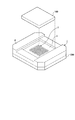
- FIG. 1 is a perspective view showing a schematic configuration of a socket according to one usage mode of an alloy material according to an embodiment of the present invention.
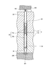
- FIG. 2 is a partial cross-sectional view showing a configuration of a main part of the socket according to one usage mode of the alloy material according to the embodiment of the present invention.
- FIG. 3 is a partial cross-sectional view showing a configuration of a main part of the socket at the time of inspection of the socket according to one usage mode of the alloy material according to the embodiment of the present invention.
- the alloy material according to the embodiment of the present invention includes a ternary alloy of silver (Ag) -palladium (Pd) -copper (Cu).
- the ternary alloy of Ag—Pd—Cu according to the present embodiment is 20 wt% Ag-40 wt% Pd-40 wt% Cu, 30 wt% Ag-35 wt% Pd-35 wt% Cu, 20 wt% Ag-55 wt% Pd-25 wt. It is an alloy formed in the region of% Cu, 30 wt% Ag-50 wt% Pd-20 wt% Cu.
- the Ag—Pd—Cu ternary alloy according to the present embodiment is an alloy in which Ag is 20 to 30 wt%, Pd is 35 to 55 wt%, and Cu is 20 to 40 wt%.
- the alloy composition has such a weight ratio, spinodal decomposition that causes two phases of ⁇ 2 (Ag) of silver rich phase and ⁇ of PdCu to appear is caused by aging treatment, and other appearance phases are mixed as much as possible. It is also preferable not to let it. For these reasons, it is necessary to limit the composition range of the ternary alloy of Ag—Pd—Cu in order to satisfy the improvement in hardness due to the appearance phase of two phases.
- the Ag—Pd—Cu alloy forms a face-centered cubic (FCC) phase by melting Ag, Pd, and Cu in a high temperature region.
- Ag and Pd have the property of melting at high temperature and low temperature.
- Pd and Cu are melted at a high temperature range and participate in curing by forming a ⁇ phase which is a compound phase at a low temperature range.
- the Vickers hardness is about 250 at most.
- Ag and Cu have the property of separating into a copper-rich phase ⁇ 1 (Cu) and ⁇ 2 (Ag). In a specific composition range of the ternary alloy, sufficient hardness is often not obtained because various phases appear.
- tin (Sn) is added to the alloy material according to the present embodiment in the range of 0.5 to 2.5 wt% based on the composition within the composition range of the above-described ternary alloy of Ag—Pd—Cu, Further, any one of cobalt (Co), chromium (Cr) and zinc (Zn) or a combination thereof is added in the range of 0.1 to 1.0 wt%. Thereby, the Vickers hardness after the aging treatment can be increased to 480 to 560.
- the Vickers hardness is 480.
- An alloy material having a good rolling workability can be obtained.
- the composition in the composition region of the ternary alloy of Ag, Pd, and Cu, the composition is such that Ag occupies 20 to 30 wt%, Pd 35 to 55 wt%, and Cu 20 to 40 wt%.
- Sn is added in a range of 0.5 to 2.5 wt%, and one or a combination of Co, Cr and Zn or a combination thereof is added in a range of 0.1 to 1.0 wt%, Ir
- 0.01 to 0.1 wt% of any one or a combination of Ru is added, so that the conductivity is excellent, and the contact probe has high hardness and high rolling properties and machinability. An excellent alloy material can be obtained.
- a ternary alloy of Ag—Pd—Cu based on Ag, Pd, and Cu Vickers hardness or conductivity as a contact probe for a semiconductor inspection apparatus is used for this ternary alloy. It was possible to find an additive metal for ensuring the above.
- the aging treatment material has a Vickers hardness of 480 to 560, improving wear resistance as an alloy material, and semiconductor inspection It is suitable for the material of the machine.
- the alloy material according to the present embodiment achieves a composition balance having conductivity and oxidation resistance while ensuring high hardness characteristics.
- the proportions relating to the alloy material of the present embodiment are 20 wt% Ag-40 wt% Pd-40 wt% Cu, 30 wt% Ag-35 wt% Pd-35 wt% Cu, 20 wt% Ag-55 wt%, assuming that high hardness is satisfied.
- Sn addition is less than 0.5 wt%, the improvement in hardness is small.
- Sn addition exceeds 2.5 wt%, rolling workability deteriorates. Therefore, Sn is preferably added in the range of 0.5 to 2.5 wt%.
- any one of Co, Cr and Zn, or a combination thereof can be added in the range of 0.1 to 1.0 wt%.
- These additive metals are useful for machinability.
- the addition amount of any one of Co, Cr and Zn or a combination thereof is less than 0.1 wt%, the improvement in cutting workability is small.
- it exceeds 1.0 wt% rolling workability deteriorates. Therefore, an appropriate amount is in the range of 0.1 to 1.0 wt%.
- 0.01 to 0.1 wt% of one or a combination of Ir and Ru can be further added.
- These additive metals are useful for workability, and fine cracks on the alloy surface are reduced during rolling as compared with those not added, and workability is improved.
- the effect of changing the amount of any one of Ir and Ru, or a combination thereof, is not less than 0.1 wt%, and therefore the appropriate amount is 0.01 to 0.1 wt%. This is because Ir and Ru have the effect of refining crystal grains, and if the crystal grains are small, it is difficult for grain boundary cracks to occur during rolling.
- the alloy material according to this embodiment can further contain 0.003 to 0.03 wt% of P.
- P addition is useful for improving the hardness.
- the addition amount of P is less than 0.003 wt%, the improvement in hardness is small.
- embrittlement occurs during solution treatment, and workability deteriorates. Therefore, an appropriate amount is in the range of 0.003 to 0.03 wt%.
- Vickers hardness shows age hardening by solution treatment of the cast and heating.
- the alloy material according to the present embodiment can be made at a lower material cost than an alloy mainly composed of platinum (Pt) or gold (Au).
- FIG. 1 is a perspective view showing a schematic configuration of a socket (contact probe) according to one usage mode of an alloy material according to an embodiment of the present invention.
- a socket 1 shown in FIG. 1 is a device that is used when an electrical characteristic test is performed on a semiconductor integrated circuit 100 that is an object to be tested, and a circuit board that outputs a test signal to the semiconductor integrated circuit 100 and the semiconductor integrated circuit 100.
- 200 is an apparatus for electrically connecting to 200.
- the socket 1 is in contact with one electrode (contact object) of the semiconductor integrated circuit 100 which is a contacted body on one end side in the longitudinal direction, and the electrode (contact object) on the circuit board 200 on the other end side.
- a plurality of contact probes 2 (hereinafter simply referred to as “probes 2”) that contact each other, a probe holder 3 that accommodates and holds the plurality of probes 2 according to a predetermined pattern, and a probe holder 3 that is provided around the probe holder 3 for inspection.
- a holder member 4 that suppresses the displacement of the semiconductor integrated circuit 100 that contacts the plurality of probes 2 at the time.
- FIG. 2 is a partial cross-sectional view showing the configuration of the main part of the socket (contact probe) according to one usage mode of the alloy material of the present embodiment, and shows the detailed configuration of the probe 2 accommodated in the probe holder 3.
- the probe 2 shown in FIG. 2 contacts the first plunger 21 that contacts the connection electrode of the semiconductor integrated circuit 100 and the electrode 201 of the circuit board 200 that includes the inspection circuit.
- a coil spring 23 provided between the first plunger 21 and the second plunger 22 to connect the first plunger 21 and the second plunger 22 so as to be extendable and contractible.
- the first plunger 21 and the second plunger 22 and the coil spring 23 constituting the probe 2 have the same axis.
- the coil spring 23 expands and contracts in the axial direction, so that the impact on the connection electrode of the semiconductor integrated circuit 100 is reduced, and the semiconductor integrated circuit 100 and the circuit board 200 are reduced. Apply load.
- the coil spring 23 has a contraction amount of the rough winding portion 23b when a predetermined load is applied, for example, in a state where the probe 2 is accommodated in the probe holder 3 when the initial load is applied (see FIG. 1).
- the diameter of the wire or the diameter of the wire is designed so that the spring characteristic becomes larger than the shortest distance between the proximal end portion of the second plunger 22 and the tightly wound portion 23a.
- the base end portion 22d is brought into sliding contact with the tightly wound portion 23a, and the proximal end portion 22d and the tightly wound portion 23a are in contact with each other. Can be electrically connected.
- the probe holder 3 is formed using an insulating material such as resin, machinable ceramics, or silicon, and a first member 31 located on the upper surface side and a second member 32 located on the lower surface side in FIG. 2 are laminated. Become.
- the first member 31 and the second member 32 are formed with the same number of holder holes 33 and 34 for receiving the plurality of probes 2, and the holder holes 33 and 34 for receiving the probes 2 have the same axis. It is formed as follows. The formation positions of the holder holes 33 and 34 are determined according to the wiring pattern of the semiconductor integrated circuit 100.
- FIG. 3 is a partial cross-sectional view showing the configuration of the main part of the socket at the time of inspection of the semiconductor integrated circuit of the socket (contact probe) according to one use mode of the alloy material of the present embodiment. It is a figure which shows the state at the time of the test
- FIG. 3 When the coil spring 23 is compressed during the inspection of the semiconductor integrated circuit 100, as shown in FIG. 3, the base end portion 22d of the second plunger 22 is in sliding contact with the inner peripheral side of the tightly wound portion 23a. At this time, the inspection signal supplied from the circuit board 200 to the semiconductor integrated circuit 100 reaches the connection electrode 101 of the semiconductor integrated circuit 100 via the second plunger 22, the tightly wound portion 23 a, and the first plunger 21.
- the coil spring has been described as having a coarsely wound portion and a tightly wound portion. However, a coil spring consisting of only a coarsely wound portion may be used.
- the tip of the first plunger 21 is tapered, even if an oxide film is formed on the surface of the connection electrode 101, the oxide film is broken through and the tip of the first plunger 21 is connected. Direct contact with the electrode 101 is possible.
- the structure of the probe 2 demonstrated here is only an example to the last, and it is possible to apply the alloy material mentioned above to various kinds of probes known conventionally.
- the probe is not limited to a plunger and a coil spring as described above, a probe having a pipe member, a pogo pin, a wire probe that obtains a load by bending a wire into a bow shape, and electrical contacts are connected to each other.
- a connection terminal may be used.
- connection terminal connects the electrical contacts to each other.
- the conductive two terminals that are in contact with the electrical contacts and the terminals can be slid.
- a holding elastic member or holding member).
- at least the terminal is made of the alloy material described above.
- Hardness test pieces were prepared by solution treatment and aging treatment. Then, the Vickers hardness (aging material hardness) of the produced test piece was measured.
- the test piece for electrical conductivity was prepared by solution treatment and aging treatment. Then, the resistance value of the produced test piece was measured and electric conductivity was calculated
- the evaluation standard for cutting workability was processed into a pin shape, and “ ⁇ ” if it was within the machining dimension tolerance, and “X” if it was outside the tolerance.
- Table 1 shows the weight ratio (composition) of the alloy materials according to Examples 1 to 15 and Comparative Examples 1 to 7 and the measurement results.
- the weight ratio was such that Ag was 20 to 30 wt% (20.00 to 29.50 wt%), Pd was 35 to 55 wt% (35.00 to 53.50 wt%), and Cu was 20 to Based on an Ag—Pd—Cu ternary alloy composed of 40 wt% (20.35 to 38.49 wt%), Sn is added in a range of 0.5 to 2.5 wt%, and Co, Cr and Zn are further added. Any one or a combination thereof is added in the range of 0.1 to 1.0 wt%, and any one of Ir and Ru or a combination thereof is added in an amount of 0.01 to 0.1 wt%.
- Examples 14 to 15 are compositions in which 0.003 to 0.03 wt% of P is further added to the above alloy composition.
- Comparative Example 1 is an Ag—Pd—Cu ternary alloy having a weight ratio of 20 to 30 wt% Ag, 35 to 55 wt% Pd, and 20 to 40 wt% Cu.
- Comparative Example 2 has a composition deviating from the present embodiment in which Co, Cr and Zn are not added.
- Comparative Examples 3 to 6 are compositions in which Sn, Co, Cr, and Zn deviate from the composition range according to the present embodiment.
- Comparative Example 7 is a composition in which P deviates from the composition range according to the present embodiment.
- Examples 1 to 13 are based on an Ag—Pd—Cu ternary alloy consisting of Ag—Pd—Cu consisting of 20 to 30 wt% Ag, 35 to 55 wt% Pd, and 20 to 40 wt% Cu. 0.5 to 2.5 wt% is added, and one or more of Co, Cr and Zn or a combination thereof is added in the range of 0.1 to 1.0 wt%, and any one of Ir and Ru Alternatively, a composition in which 0.01 to 0.1 wt% of these combinations are added.
- Example 1 the Vickers hardness after the aging treatment was in the range of 480 to 560, and the rolling and cutting workability were also good. According to this result, the addition of Sn, Co, Cr, Zn, Ir, and Ru is involved in improving the Vickers hardness as compared with Comparative Example 1 in which Sn, Co, Cr, Zn, Ir, and Ru are not added. It was confirmed.
- Example 14 is a composition obtained by adding 0.003 wt% of P to Example 7
- Example 15 is a composition obtained by adding 0.03 wt% of P to Example 10.
- the addition of P was involved in improving Vickers hardness.
- the content of Pd is reduced with the addition of P.
- the Cu content was decreased with the addition of P.
- Comparative Example 2 is a composition in which 2.5 wt% Sn and 0.05 wt% Ir are added to the Ag—Pd—Cu ternary alloy in the composition range according to the present embodiment. While improvement was obtained, the machinability deteriorated as compared with Examples 1 to 15 to which Co, Cr and Zn were added. It was confirmed that the addition of Co, Cr, and Zn is involved in improving the machinability.
- Comparative Examples 3 to 6 are compositions added in excess of Sn, Co, Cr, and Zn from the composition range according to the present embodiment, and while improvement in hardness was obtained, Examples 1 to 15 Compared with the rolling processability.
- Comparative Example 7 was a composition added in excess of P from the composition range according to the present embodiment, and the workability deteriorated as compared with Examples 1 to 15.
- the alloy material according to the present invention, the contact probe and the connection terminal made of the alloy material are useful for contact probes in terms of conductivity, hardness and workability.
Landscapes
- Chemical & Material Sciences (AREA)
- Metallurgy (AREA)
- Engineering & Computer Science (AREA)
- Materials Engineering (AREA)
- Mechanical Engineering (AREA)
- Organic Chemistry (AREA)
- Physics & Mathematics (AREA)
- Thermal Sciences (AREA)
- Crystallography & Structural Chemistry (AREA)
- General Physics & Mathematics (AREA)
- Measuring Leads Or Probes (AREA)
- Testing Of Individual Semiconductor Devices (AREA)
- Connecting Device With Holders (AREA)
- Contacts (AREA)
Abstract
Description

2 コンタクトプローブ(プローブ)
3 プローブホルダ
4 ホルダ部材
21 第1プランジャ
22 第2プランジャ
23 コイルばね
23a 密着巻き部
23b 粗巻き部
31 第1部材
32 第2部材
33,34 ホルダ孔
100 半導体集積回路
101 接続用電極
200 回路基板
201 電極
Claims (6)
- 銀(Ag)、パラジウム(Pd)、銅(Cu)の3元合金の組成領域において、Agが20~30wt%、Pdが35~55wt%、Cuが20~40wt%を占める組成とし、該組成を基本として、スズ(Sn)を0.5~2.5wt%の範囲で添加し、さらにコバルト(Co)、クロム(Cr)および亜鉛(Zn)のいずれか1つ若しくはこれらの組み合わせを0.1~1.0wt%の範囲で添加するとともに、イリジウム(Ir)およびルテニウム(Ru)のいずれか1つ若しくはこれらの組み合わせを0.01~0.1wt%添加してなることを特徴とする合金材料。
- リン(P)を0.003~0.03wt%さらに添加してなることを特徴とする請求項1に記載の合金材料。
- 加熱により時効処理させたビッカース硬さが、480~560であることを特徴とする請求項1または2に記載の合金材料。
- 長手方向の両端で接触対象とそれぞれ接触する導電性のコンタクトプローブであって、
少なくとも一部が、請求項1~3のいずれか一つに記載の合金材料を用いて形成されたことを特徴とするコンタクトプローブ。 - 一端で一方の接触対象と接触する導電性の第1プランジャと、
一端で他方の接触対象と接触する導電性の第2プランジャと、
前記第1および第2プランジャの間に設けられて該第1および第2プランジャを伸縮自在に連結するコイルばねと、を有し、
前記第1プランジャ、前記第2プランジャおよび前記コイルばねのうち、少なくとも一つが前記合金材料からなることを特徴とする請求項4に記載のコンタクトプローブ。 - 長手方向の両端で接触対象とそれぞれ接触する導電性の接続端子であって、
少なくとも一部が、請求項1~3のいずれか一つに記載の合金材料を用いて形成されたことを特徴とする接続端子。
Priority Applications (4)
| Application Number | Priority Date | Filing Date | Title |
|---|---|---|---|
| JP2017510230A JP6550457B2 (ja) | 2015-03-31 | 2016-03-31 | 合金材料、コンタクトプローブおよび接続端子 |
| SG11201708015XA SG11201708015XA (en) | 2015-03-31 | 2016-03-31 | Alloy material, contact probe, and connection terminal |
| US15/562,580 US10889878B2 (en) | 2015-03-31 | 2016-03-31 | Alloy material, contact probe, and connection terminal |
| PH12017501772A PH12017501772A1 (en) | 2015-03-31 | 2017-09-26 | Alloy materrial, contact probe, and connection terminal |
Applications Claiming Priority (2)
| Application Number | Priority Date | Filing Date | Title |
|---|---|---|---|
| JP2015-074330 | 2015-03-31 | ||
| JP2015074330 | 2015-03-31 |
Publications (1)
| Publication Number | Publication Date |
|---|---|
| WO2016159315A1 true WO2016159315A1 (ja) | 2016-10-06 |
Family
ID=57004422
Family Applications (1)
| Application Number | Title | Priority Date | Filing Date |
|---|---|---|---|
| PCT/JP2016/060829 Ceased WO2016159315A1 (ja) | 2015-03-31 | 2016-03-31 | 合金材料、コンタクトプローブおよび接続端子 |
Country Status (6)
| Country | Link |
|---|---|
| US (1) | US10889878B2 (ja) |
| JP (1) | JP6550457B2 (ja) |
| PH (1) | PH12017501772A1 (ja) |
| SG (1) | SG11201708015XA (ja) |
| TW (1) | TWI567207B (ja) |
| WO (1) | WO2016159315A1 (ja) |
Cited By (3)
| Publication number | Priority date | Publication date | Assignee | Title |
|---|---|---|---|---|
| EP3960890A1 (de) * | 2020-09-01 | 2022-03-02 | Heraeus Deutschland GmbH & Co. KG | Palladium-kupfer-silber-ruthenium-legierung |
| JP2023126154A (ja) * | 2022-02-28 | 2023-09-07 | ヘレウス ドイチェラント ゲーエムベーハー ウント カンパニー カーゲー | パラジウム-銅-銀合金 |
| JP7625115B1 (ja) * | 2024-04-26 | 2025-01-31 | 田中貴金属工業株式会社 | Ag-Pd-Cu系合金からなるプローブピン用材料及びプローブピン |
Families Citing this family (5)
| Publication number | Priority date | Publication date | Assignee | Title |
|---|---|---|---|---|
| EP3595094B1 (en) * | 2017-03-07 | 2023-05-03 | Mitsubishi Materials Corporation | Corrosion-resistant terminal material, corrosion-resistant terminal, and wire end structure |
| JP7005939B2 (ja) * | 2017-05-25 | 2022-01-24 | 日本電産リード株式会社 | コンタクトプローブ |
| EP3594756B1 (fr) * | 2018-07-10 | 2021-05-12 | Blancpain SA | Composant d'horlogerie avec partie arbrée en alliage amagnétique |
| CN117026055B (zh) * | 2023-10-09 | 2024-01-12 | 浙江金连接科技股份有限公司 | 一种半导体芯片测试探针用钯合金及其制备方法 |
| CN118374715B (zh) * | 2024-06-24 | 2024-09-06 | 汕头市骏码凯撒有限公司 | 一种晶圆测试用高强韧度耐磨耗性抗沾黏的探针材料及其制备工艺 |
Citations (4)
| Publication number | Priority date | Publication date | Assignee | Title |
|---|---|---|---|---|
| WO2013099682A1 (ja) * | 2011-12-27 | 2013-07-04 | 株式会社徳力本店 | 電気・電子機器用のPd合金 |
| WO2014021465A1 (ja) * | 2012-08-03 | 2014-02-06 | 山本貴金属地金株式会社 | 合金材料、コンタクトプローブおよび接続端子 |
| WO2014049874A1 (ja) * | 2012-09-28 | 2014-04-03 | 株式会社徳力本店 | 電気・電子機器用途のAg‐Pd‐Cu‐Co合金 |
| JP2014114465A (ja) * | 2012-12-06 | 2014-06-26 | Ishifuku Metal Ind Co Ltd | Ag基合金からなるプローブピン |
-
2016
- 2016-03-31 US US15/562,580 patent/US10889878B2/en active Active
- 2016-03-31 JP JP2017510230A patent/JP6550457B2/ja active Active
- 2016-03-31 TW TW105110495A patent/TWI567207B/zh active
- 2016-03-31 WO PCT/JP2016/060829 patent/WO2016159315A1/ja not_active Ceased
- 2016-03-31 SG SG11201708015XA patent/SG11201708015XA/en unknown
-
2017
- 2017-09-26 PH PH12017501772A patent/PH12017501772A1/en unknown
Patent Citations (4)
| Publication number | Priority date | Publication date | Assignee | Title |
|---|---|---|---|---|
| WO2013099682A1 (ja) * | 2011-12-27 | 2013-07-04 | 株式会社徳力本店 | 電気・電子機器用のPd合金 |
| WO2014021465A1 (ja) * | 2012-08-03 | 2014-02-06 | 山本貴金属地金株式会社 | 合金材料、コンタクトプローブおよび接続端子 |
| WO2014049874A1 (ja) * | 2012-09-28 | 2014-04-03 | 株式会社徳力本店 | 電気・電子機器用途のAg‐Pd‐Cu‐Co合金 |
| JP2014114465A (ja) * | 2012-12-06 | 2014-06-26 | Ishifuku Metal Ind Co Ltd | Ag基合金からなるプローブピン |
Cited By (7)
| Publication number | Priority date | Publication date | Assignee | Title |
|---|---|---|---|---|
| EP3960890A1 (de) * | 2020-09-01 | 2022-03-02 | Heraeus Deutschland GmbH & Co. KG | Palladium-kupfer-silber-ruthenium-legierung |
| US11746397B2 (en) | 2020-09-01 | 2023-09-05 | Heraeus Deutschland GmbH & Co. KG | Palladium-copper-silver-ruthenium alloy |
| JP2023126154A (ja) * | 2022-02-28 | 2023-09-07 | ヘレウス ドイチェラント ゲーエムベーハー ウント カンパニー カーゲー | パラジウム-銅-銀合金 |
| JP7526300B2 (ja) | 2022-02-28 | 2024-07-31 | ヘレウス ドイチェラント ゲーエムベーハー ウント カンパニー カーゲー | パラジウム-銅-銀合金 |
| JP7625115B1 (ja) * | 2024-04-26 | 2025-01-31 | 田中貴金属工業株式会社 | Ag-Pd-Cu系合金からなるプローブピン用材料及びプローブピン |
| JP7625115B6 (ja) | 2024-04-26 | 2025-02-21 | 田中貴金属工業株式会社 | Ag-Pd-Cu系合金からなるプローブピン用材料及びプローブピン |
| WO2025225600A1 (ja) * | 2024-04-26 | 2025-10-30 | 田中貴金属工業株式会社 | Ag-Pd-Cu系合金からなるプローブピン用材料及びプローブピン |
Also Published As
| Publication number | Publication date |
|---|---|
| US20180105902A1 (en) | 2018-04-19 |
| JPWO2016159315A1 (ja) | 2018-09-13 |
| JP6550457B2 (ja) | 2019-07-24 |
| US10889878B2 (en) | 2021-01-12 |
| SG11201708015XA (en) | 2017-10-30 |
| TW201700745A (zh) | 2017-01-01 |
| PH12017501772A1 (en) | 2018-03-19 |
| TWI567207B (zh) | 2017-01-21 |
Similar Documents
| Publication | Publication Date | Title |
|---|---|---|
| JP6647075B2 (ja) | 合金材料、コンタクトプローブおよび接続端子 | |
| JP6550457B2 (ja) | 合金材料、コンタクトプローブおよび接続端子 | |
| JP6280866B2 (ja) | 合金材料、コンタクトプローブおよび接続端子 | |
| JP6728057B2 (ja) | 合金材料、コンタクトプローブおよび接続端子 | |
| KR100718577B1 (ko) | 프로브 핀용 재료 | |
| JP4176133B1 (ja) | プローブピン | |
| KR20160053838A (ko) | 무연 땜납, 무연 땜납 볼, 이 무연 땜납을 사용한 땜납 조인트 및 이 땜납 조인트를 갖는 반도체 회로 | |
| WO2013099682A1 (ja) | 電気・電子機器用のPd合金 | |
| CN109155208B (zh) | 电触点用的覆层材料和该覆层材料的制造方法 | |
| KR20250053083A (ko) | 프로브 핀용 합금 재료 | |
| JP7798263B2 (ja) | プローブピン用合金材料 | |
| KR20230160852A (ko) | 프로브 핀용 합금 재료 | |
| WO2024142878A1 (ja) | 合金材料およびコンタクトプローブ | |
| JP2024089037A (ja) | プローブピン用合金材料 | |
| HK1210232B (en) | Alloy material, contact probe, and connection terminal | |
| JP2025074557A (ja) | Cu-Ag合金線材の製造方法及びこの製造方法により製造したCu-Ag合金線材、Cu-Ag合金線材を用いて得られた電気・電子部品検査用プローブピン | |
| JP2017027705A (ja) | コネクタ用端子およびその製造方法 | |
| CN117015625A (zh) | 探测针用合金材料 | |
| JP2005324257A (ja) | はんだ付け物品 | |
| CN101726634A (zh) | 电接触用合金材料及其探针 |
Legal Events
| Date | Code | Title | Description |
|---|---|---|---|
| 121 | Ep: the epo has been informed by wipo that ep was designated in this application |
Ref document number: 16773195 Country of ref document: EP Kind code of ref document: A1 |
|
| ENP | Entry into the national phase |
Ref document number: 2017510230 Country of ref document: JP Kind code of ref document: A |
|
| WWE | Wipo information: entry into national phase |
Ref document number: 12017501772 Country of ref document: PH |
|
| WWE | Wipo information: entry into national phase |
Ref document number: 15562580 Country of ref document: US |
|
| WWE | Wipo information: entry into national phase |
Ref document number: 11201708015X Country of ref document: SG |
|
| NENP | Non-entry into the national phase |
Ref country code: DE |
|
| 122 | Ep: pct application non-entry in european phase |
Ref document number: 16773195 Country of ref document: EP Kind code of ref document: A1 |