WO2016159068A1 - マイクロウェルアレイ及びその製造方法、マイクロ流体デバイス、マイクロウェルアレイのウェル内に水性液体を封入する方法及び水性液体の分析方法 - Google Patents
マイクロウェルアレイ及びその製造方法、マイクロ流体デバイス、マイクロウェルアレイのウェル内に水性液体を封入する方法及び水性液体の分析方法 Download PDFInfo
- Publication number
- WO2016159068A1 WO2016159068A1 PCT/JP2016/060367 JP2016060367W WO2016159068A1 WO 2016159068 A1 WO2016159068 A1 WO 2016159068A1 JP 2016060367 W JP2016060367 W JP 2016060367W WO 2016159068 A1 WO2016159068 A1 WO 2016159068A1
- Authority
- WO
- WIPO (PCT)
- Prior art keywords
- microwell array
- well
- aqueous liquid
- wells
- hydrophobic
- Prior art date
- Legal status (The legal status is an assumption and is not a legal conclusion. Google has not performed a legal analysis and makes no representation as to the accuracy of the status listed.)
- Ceased
Links
Images



Classifications
-
- B—PERFORMING OPERATIONS; TRANSPORTING
- B01—PHYSICAL OR CHEMICAL PROCESSES OR APPARATUS IN GENERAL
- B01J—CHEMICAL OR PHYSICAL PROCESSES, e.g. CATALYSIS OR COLLOID CHEMISTRY; THEIR RELEVANT APPARATUS
- B01J19/00—Chemical, physical or physico-chemical processes in general; Their relevant apparatus
-
- B—PERFORMING OPERATIONS; TRANSPORTING
- B81—MICROSTRUCTURAL TECHNOLOGY
- B81B—MICROSTRUCTURAL DEVICES OR SYSTEMS, e.g. MICROMECHANICAL DEVICES
- B81B1/00—Devices without movable or flexible elements, e.g. microcapillary devices
-
- B—PERFORMING OPERATIONS; TRANSPORTING
- B81—MICROSTRUCTURAL TECHNOLOGY
- B81C—PROCESSES OR APPARATUS SPECIALLY ADAPTED FOR THE MANUFACTURE OR TREATMENT OF MICROSTRUCTURAL DEVICES OR SYSTEMS
- B81C1/00—Manufacture or treatment of devices or systems in or on a substrate
-
- C—CHEMISTRY; METALLURGY
- C12—BIOCHEMISTRY; BEER; SPIRITS; WINE; VINEGAR; MICROBIOLOGY; ENZYMOLOGY; MUTATION OR GENETIC ENGINEERING
- C12M—APPARATUS FOR ENZYMOLOGY OR MICROBIOLOGY; APPARATUS FOR CULTURING MICROORGANISMS FOR PRODUCING BIOMASS, FOR GROWING CELLS OR FOR OBTAINING FERMENTATION OR METABOLIC PRODUCTS, i.e. BIOREACTORS OR FERMENTERS
- C12M1/00—Apparatus for enzymology or microbiology
- C12M1/34—Measuring or testing with condition measuring or sensing means, e.g. colony counters
-
- G—PHYSICS
- G01—MEASURING; TESTING
- G01N—INVESTIGATING OR ANALYSING MATERIALS BY DETERMINING THEIR CHEMICAL OR PHYSICAL PROPERTIES
- G01N21/00—Investigating or analysing materials by the use of optical means, i.e. using sub-millimetre waves, infrared, visible or ultraviolet light
- G01N21/01—Arrangements or apparatus for facilitating the optical investigation
- G01N21/03—Cuvette constructions
-
- G—PHYSICS
- G01—MEASURING; TESTING
- G01N—INVESTIGATING OR ANALYSING MATERIALS BY DETERMINING THEIR CHEMICAL OR PHYSICAL PROPERTIES
- G01N21/00—Investigating or analysing materials by the use of optical means, i.e. using sub-millimetre waves, infrared, visible or ultraviolet light
- G01N21/62—Systems in which the material investigated is excited whereby it emits light or causes a change in wavelength of the incident light
- G01N21/63—Systems in which the material investigated is excited whereby it emits light or causes a change in wavelength of the incident light optically excited
- G01N21/64—Fluorescence; Phosphorescence
-
- G—PHYSICS
- G01—MEASURING; TESTING
- G01N—INVESTIGATING OR ANALYSING MATERIALS BY DETERMINING THEIR CHEMICAL OR PHYSICAL PROPERTIES
- G01N37/00—Details not covered by any other group of this subclass
Definitions
- the present invention relates to a microwell array and a manufacturing method thereof, a microfluidic device, a method for enclosing an aqueous liquid in the wells of the microwell array, and a method for analyzing an aqueous liquid.
- microwell arrays having various types of fine channel structures formed by using etching techniques, photolithography techniques, and the like used in semiconductor circuit manufacturing techniques have been studied.
- the wells of these microwell arrays are used as chemical reaction vessels for causing various biochemical or chemical reactions in a small volume of fluid.
- Patent Documents 1 to 4 describe the use of such a microfluidic system as various microchips and biochips.
- digital PCR technology involves PCR amplification by dividing a mixture of a reagent and nucleic acid into countless microdroplets so that a signal such as fluorescence can be detected from the droplet containing nucleic acid. This is a technique for performing quantification by counting the number of detected droplets.
- a method for producing a microdroplet As a method for producing a microdroplet, a method for producing a microdroplet by dividing with a sealing liquid, or a reagent is put into a hole formed on a substrate, and then a microdroplet is made by adding a sealing liquid.
- a manufacturing method (see, for example, Patent Document 4) has been studied.
- the microwell array according to the first aspect of the present invention includes a plurality of wells having a hydrophilic portion and a hydrophobic portion on the well surface.
- the capacity of each of the plurality of wells may be 1 fL to 6 nL.
- the density of the plurality of wells may be 100,000 to 10 million / cm 2 .
- the plurality of wells may have the hydrophobic portion at the top of the well and have the hydrophilic portion at a position closer to the well bottom than the hydrophobic portion.
- the plurality of wells may be provided on a substrate that is transparent to electromagnetic waves.
- the electromagnetic waves may be X-rays, ultraviolet rays, visible rays, or infrared rays.
- the substrate may be formed of a material that does not substantially have autofluorescence.
- the contact angle of the hydrophilic portion measured in accordance with the sessile drop method defined in JIS R3257-1999 may be less than 70 degrees.
- the hydrophilic portion may be formed of a siloxane polymer.
- the contact angle of the hydrophobic part measured according to the sessile drop method defined in JIS R3257-1999 may be 70 degrees or more.
- the hydrophobic portion may be formed of a novolac resin.
- the microfluidic device includes a flow path and the microwell array according to the above aspect disposed in the flow path.
- a method for enclosing an aqueous liquid in a well by preparing a microfluidic device including a flow path and the microwell array according to the above aspect disposed in the flow path.
- An aqueous liquid is sent to the flow path of the fluidic device, the aqueous liquid is introduced to the well of the microwell array, a sealing liquid is sent to the flow path, and the aqueous liquid introduced into the well A sealing liquid layer is formed on the upper layer, and the aqueous liquid is sealed in the well.
- the method for producing a microwell array according to the fourth aspect of the present invention includes forming a hydrophilic layer by laminating a hydrophilic material on a substrate having electromagnetic wave permeability, and laminating a hydrophobic material on the hydrophilic layer. Forming a layer and drilling the hydrophobic layer to form a plurality of wells;
- the plurality of wells may be formed by excavating the hydrophobic layer and the hydrophilic layer.
- the method for analyzing an aqueous liquid according to the fifth aspect of the present invention detects the fluorescence or phosphorescence emitted from the well by irradiating electromagnetic waves to the wells of the microwell array according to the above aspect in which the aqueous liquid is enclosed.
- the fluorescence or the phosphorescence may be detected on the substrate of the microwell array according to the above aspect.
- a microwell array in which an aqueous liquid can be easily sealed in a well.
- the manufacturing method of the microwell array which concerns on the said aspect, a microfluidic device, the method of enclosing aqueous liquid in the well of a microwell array, and the analysis method of aqueous liquid can be provided.
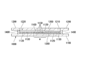
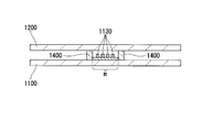
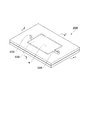
- FIG. 1A is a perspective view showing a microfluidic device according to a second embodiment.
- 1B is a cross-sectional view taken along line bb in the microfluidic device of FIG. 1A.
- 1C is a cross-sectional view taken along line cc of the microfluidic device of FIG. 1A.
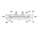
- FIG. 2A is a perspective view showing a microfluidic device according to a third embodiment.
- 2B is a cross-sectional view taken along line bb in the microfluidic device of FIG. 2A.
- 2C is a cross-sectional view taken along line cc in the microfluidic device of FIG. 2A. It is sectional drawing which shows the structure of the microwell array concerning 5th Embodiment.
- FIG. 6 is a cross-sectional view showing the structure of a microwell array of Comparative Example 1.
- FIG. It is sectional drawing which shows the state which enclosed the aqueous liquid in the microwell array of the microfluidic device of Experimental example 1.
- FIG. It is a photograph which shows the result of having observed the microwell array of the microfluidic device of Experimental example 1 from the board
- FIG. It is sectional drawing which shows the state which enclosed the aqueous liquid in the microwell array of the microfluidic device of Experimental example 2.
- FIG. It is a photograph which shows the result of having observed the microwell array of the microfluidic device of Experimental example 2 from the board
- the first embodiment of the present invention provides a microwell array comprising a plurality of wells having a hydrophilic portion and a hydrophobic portion on a well surface.
- enclosing the aqueous liquid means introducing the aqueous liquid into a plurality of wells constituting the microwell array, and further isolating the liquids introduced into the wells so as not to be mixed with each other.
- the isolation method include forming an oil layer on the upper portion of the well after introducing an aqueous liquid into the well.
- microwell array it is possible to easily enclose an aqueous liquid in 90% or more, for example, 95% or more, for example, 99% or more, for example, 100%, of the plurality of wells constituting the microwell array. .
- the volume per well is, for example, 1 femtoliter (fL) to 6 nanoliters (nL), preferably 1 fL to 5 picoliters (pL), and more preferably Is 1 fL to 300 fL.
- an enzymatic reaction such as digital PCR or invader reaction can be suitably performed.
- gene mutation detection can be performed by the digital PCR.
- the reaction volume is smaller even if the number of wells is the same.
- the material of the microwell array is preferably a material that does not inhibit the enzyme reaction.
- the shape and size of the wells of the microwell array are not particularly limited. For example, when various biochemical reactions are performed in microdroplets, one to several biomolecules or carriers can be accommodated. It preferably has a shape and size.
- the carrier may be a bead, for example, and a biomolecule as a sample may be bound to the carrier.
- the shape of the well is, for example, a cylindrical shape, a polyhedron composed of a plurality of surfaces (eg, rectangular parallelepiped, hexagonal prism, octagonal prism, etc.), inverted cone, inverted pyramid (inverted triangular pyramid, inverted quadrangular pyramid, inverted A pentagonal pyramid, an inverted hexagonal pyramid, an inverted polygonal pyramid with a heptagon or more), or a combination of two or more of these shapes.
- a cylindrical shape a polyhedron composed of a plurality of surfaces (eg, rectangular parallelepiped, hexagonal prism, octagonal prism, etc.), inverted cone, inverted pyramid (inverted triangular pyramid, inverted quadrangular pyramid, inverted A pentagonal pyramid, an inverted hexagonal pyramid, an inverted polygonal pyramid with a heptagon or more), or a combination of two or more of these shapes.
- a part may be cylindrical and the rest may be an inverted cone.
- the bottom of the cone or pyramid is the entrance (opening) of the well, but the reverse cone shape or the inverted pyramid shape may be partially cut off from the top. .
- the bottom of the microwell is flat.
- the bottom of the microwell is usually flat, but may be a curved surface (convex surface or concave surface).
- the bottom of the microwell can be curved as in the case of a shape obtained by cutting a part from the top of an inverted cone or inverted pyramid.
- the diameter When the well is cylindrical, the diameter may be 3 to 10 ⁇ m for the purpose of enclosing an aqueous liquid containing biomolecules.
- the depth may be 3 to 10 ⁇ m.
- the size of a carrier such as a bead to which a biomolecule is attached, and a suitable ratio between the dimensions of the well, etc., the size of the well is one per microwell, or It is determined appropriately so that several biomolecules are accommodated.
- the detection target to be detected using the microwell array according to the present embodiment may be, for example, a sample collected from a living body such as blood, a PCR product, or the like, or an artificially synthesized compound or the like.
- the well may have a shape and size that allow one molecule of DNA to enter.
- biomolecules include proteins, RNA (including RNA such as miRNA, mtRNA, tRNA), sugars, and amino acids (including peptides).
- the density of a plurality of wells is, for example, 100,000 to 10 million pieces / cm 2 , preferably 100,000 to 5 million pieces / cm 2 , and more preferably 100,000. ⁇ 1 million pieces / cm 2 .
- the density of the well is in such a range (100,000 to 10,000,000 / cm 2 )
- the presence ratio of the mutation to be detected to the wild type is about 0.01%, about 100,000 to 5 million pieces / cm 2 , more preferably 100,000 to 1 million.
- the number of cells / cm 2 is present, rapid measurement is possible even if all wells are detected without impairing the detection accuracy.
- each well (out of a plurality of wells) has the hydrophobic portion at the top of the well, and the hydrophilic portion is positioned closer to the well bottom (bottom side) than the hydrophobic portion. It is preferable to have a sex part. As will be described later, the inventors have found that such a configuration makes it very easy to enclose an aqueous liquid in the wells of the microwell array.
- the above-mentioned hydrophilic part (material of the hydrophilic part) may have a contact angle of less than 70 degrees measured according to the sessile drop method defined in JIS R3257-1999.
- being hydrophilic means that the contact angle measured according to the sessile drop method defined in JIS R3257-1999 is less than 70 degrees.
- the hydrophobic part (the material of the hydrophobic part) may have a contact angle of 70 degrees or more measured according to the sessile drop method defined in JIS R3257-1999.
- being hydrophobic means that the contact angle measured according to the sessile drop method specified in JIS R3257-1999 is 70 degrees or more.
- hydrophilic resin The resin forming the hydrophilic portion (hereinafter sometimes referred to as “hydrophilic resin”) is not particularly limited as long as the effect of the present invention is exerted. Examples thereof include resins having a group. Examples of the hydrophilic group include a hydroxyl group, a carboxyl group, a sulfone group, a sulfonyl group, an amino group, an amide group, an ether group, and an ester group.
- a siloxane polymer an epoxy resin; a polyethylene resin; a polyester resin; a polyurethane resin; a polyacrylamide resin; a polyvinylpyrrolidone resin; an acrylic resin such as a polyacrylic acid copolymer; a cationized polyvinyl alcohol, a silanolated polyvinyl alcohol, Polyvinyl alcohol resins such as sulfonated polyvinyl alcohol; polyvinyl acetal resins; polyvinyl butyral resins; polyethylene polyamide resins; polyamide polyamine resins; cellulose derivatives such as hydroxymethyl cellulose and methyl cellulose; polyalkylenes such as polyethylene oxide and polyethylene oxide-polypropylene oxide copolymers Oxide derivatives; maleic anhydride copolymer; ethylene-vinyl acetate copolymer; At least one resin having a contact angle of less than 70 degrees measured according to the sessile drop method specified in JIS R3257-1999 is
- the hydrophilic resin may be a thermoplastic resin, a thermosetting resin, a resin curable by an active energy ray such as an electron beam or UV light, or an elastomer. .
- the hydrophilic layer may also have a function of bringing the substrate and the hydrophobic layer into close contact when a substrate described later is present.
- the hydrophilic layer may be formed by applying a thermosetting silane coupling agent or the like to the substrate and thermally curing to form a siloxane polymer.
- hydrophobic resin The resin that forms the hydrophobic portion (hereinafter sometimes referred to as “hydrophobic resin”) is not particularly limited as long as the effects of the present invention are exhibited.
- novolak resin acrylic resin; methacrylic resin; styrene resin; Polyvinyl resin; Polyamide resin; Polyacetal resin; Polycarbonate resin; Polyphenylene sulfide resin; Polysulfone resin; Fluorine resin; Silicone resin; Yuria resin; Melamine resin; Any of the above resin combinations can be appropriately selected from at least one resin having a contact angle of 70 degrees or more measured according to the sessile drop method defined in JIS R3257-1999. .
- the hydrophobic resin may be a thermoplastic resin, a thermosetting resin, a resin curable by an active energy ray such as an electron beam or UV light, or an elastomer. .
- the hydrophobic portion may be formed of a resist, for example.
- the resist may be a photoresist from the viewpoint of easily forming a fine structure.
- the photoresist may be, for example, a photosensitive novolac resin.
- the microwell array according to this embodiment may be formed on a substrate.
- the substrate may be a substrate having electromagnetic wave permeability or a substrate having no electromagnetic wave permeability.
- examples of the electromagnetic wave include X-rays, ultraviolet rays, visible rays, and infrared rays.
- electromagnetic waves can be used to analyze the results of experiments performed on the microwell array. For example, fluorescence, phosphorescence, and the like generated as a result of irradiation with electromagnetic waves can be measured from the substrate side (via the substrate and on the substrate).
- the fluorescence and phosphorescence include light having different wavelengths at the time of irradiation and detection (wavelengths are converted).
- wavelength conversion include a case where fluorescence or phosphorescence in the visible light region is generated as a result of irradiation with ultraviolet light, and a case where fluorescence or phosphorescence in the infrared region is generated as a result of irradiation with visible light.
- a fluorescence microscope can be used.
- the electromagnetic wave may be irradiated, for example, from the substrate side (to the substrate), or may be irradiated, for example, from the entrance side of the well (to the entrance of the well).
- Examples of the substrate having electromagnetic wave permeability include glass and resin.
- Examples of the resin substrate include ABS resin, polycarbonate resin, COC (cycloolefin copolymer), COP (cycloolefin polymer), acrylic resin, polyvinyl chloride, polystyrene resin, polyethylene resin, polypropylene resin, polyvinyl acetate, and PET (polyethylene). Terephthalate), PEN (polyethylene naphthalate) and the like. These resins may contain various additives, and a plurality of resins may be mixed.
- the substrate does not substantially have autofluorescence.
- substantially having no autofluorescence means that the substrate has no autofluorescence of the wavelength used for detection of the experimental results, or even if it has autofluorescence, the detection of the experimental results is affected. It means that it is so weak as not. For example, if the autofluorescence is about 1/10 or less and 1/100 or less as compared with the fluorescence to be detected, it can be said that it is so weak that it does not affect the detection of the experimental result.
- quartz glass As a material that has electromagnetic wave transparency and does not emit autofluorescence at all, for example, quartz glass can be cited.
- materials that have weak autofluorescence and that do not interfere with detection of experimental results using electromagnetic waves include low fluorescent glass, acrylic resin, COC (cycloolefin copolymer), and COP (cycloolefin polymer).
- fluorescent substances such as fluorescent dyes, FRET (fluorescence resonance energy transfer), reaction of fluorescently labeled avidin and streptavidin, enzyme reaction using horseradish peroxidase, FRET such as Invader (registered trademark) method
- FRET fluorescent resonance energy transfer
- Invader registered trademark
- the observation of the fluorescence emitted from the biomolecule accommodated in the well can be performed from the substrate side of the microwell array (via the substrate and from the substrate) using, for example, an inverted microscope.
- the number of target molecules can be specified by counting the number of microwells emitting predetermined fluorescence.
- the biomolecule may be treated with a fluorescent label that specifically labels the target molecule before being accommodated in the well.
- the bead is accommodated in the well and brought into contact with a fluorescent label capable of specifically labeling the target molecule, and the target molecule is placed in the well. May be fluorescently labeled.
- the thickness of the substrate can be appropriately determined.
- the fluorescence is observed from the substrate side (on the substrate) using a fluorescence microscope, it is, for example, 5 mm or less, for example, 2 mm or less, for example, 1.6 mm or less. Is preferred.
- Turbidity can be used in addition to fluorescence. Turbidity can be measured, for example, by the transmittance of light having a wavelength of about 400 to 1000 nm in the detection target.
- Microfluidic device One embodiment of the present invention provides a microfluidic device comprising a flow path and the above-described microwell array disposed in the flow path. By using such a microfluidic device, it becomes easy to enclose an aqueous liquid in the wells of the microwell array.
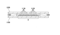
- FIG. 1A is a perspective view showing a microfluidic device according to a second embodiment.
- 1B is a cross-sectional view taken along line bb in the microfluidic device of FIG. 1A.
- 1C is a cross-sectional view taken along line cc of the microfluidic device of FIG. 1A.
- the microfluidic device 1000 includes a bottom member 1100, a lid member 1200, a flow channel 1300, a flow channel inlet 1210 provided at one end (first end) of the flow channel 1300, and the flow channel 1300.
- a flow path outlet 1220 provided at the other end (second end), a sealing member 1400 that forms part of the inner wall of the flow path 1300, and a microwell array m disposed inside the flow path 1300 are provided.
- the fluid may be introduced from the channel inlet 1210 and discharged from the channel outlet 1220 using a syringe or the like.
- the microwell array m is provided inside the flow path 1300.
- the structure of the microwell array m will be described later.
- the substrate 1100 of the microwell array m and the bottom member 1100 of the microfluidic device 1000 may be integrated. Further, the hydrophilic layer 1120 and the hydrophobic layer 1130 of the microwell array m may be integrally formed on the bottom member 1100 of the microfluidic device 1000. That is, the microwell array m may be formed on the bottom member 1100 of the microfluidic device 1000.
- the same material as that of the substrate of the microwell array described above can be used.
- the material of the sealing member 1400 is not particularly limited.
- a double-sided pressure-sensitive adhesive tape in which an acrylic pressure-sensitive adhesive is laminated on both sides of a core material film formed of silicone rubber or acrylic foam, or an adhesive is laminated.
- spacer members resin, metal, paper, inorganic materials such as glass
- these sealing members those which do not easily react with the liquid to be fed can be appropriately selected.
- what coated the surface of the sealing member so that it may become difficult to react with the liquid sent can also be employ
- a double-sided adhesive tape was used.
- FIG. 2A is a perspective view showing a microfluidic device according to a third embodiment of the present invention.
- 2B is a cross-sectional view taken along line bb in the microfluidic device of FIG. 2A.
- 2C is a cross-sectional view taken along line cc in the microfluidic device of FIG. 2A.
- the microfluidic device 2000 has a configuration in which a part of the flow channel 1300 is enlarged in a plan view of the microfluidic device 1000 according to the first embodiment described above.
- the microwell array m (second microwell array m-2) in the microfluidic device 2000 has a larger area in plan view than the microwell array m in the microfluidic device 1000.
- Other configurations of the microfluidic device 2000 are the same as those of the microfluidic device 1000.
- plan view means a state in which the microfluidic device or the microwell array is viewed from a direction perpendicular to the bottom member of the microfluidic device or the substrate of the microwell array.
- a microfluidic device including a flow path and the microwell array according to the above-described embodiment disposed in the flow path is prepared, and the flow path of the microfluidic device is aqueous. Liquid is fed, the aqueous liquid is introduced into the wells of the microwell array, the sealing liquid is fed into the flow path, and the sealing liquid layer is formed on the upper layer of the aqueous liquid introduced into the well.
- a method is provided for encapsulating an aqueous liquid within a well of a microwell array, wherein the aqueous liquid is encapsulated within the well.
- the aqueous liquid means water, a biological sample such as a buffer solution containing a biomolecule to be detected, an enzyme reaction solution, or the like.
- the biological sample is generally an aqueous liquid.
- the aqueous liquid may be, for example, a PCR reaction solution containing a biological sample as a template and SYBR Green as a detection reagent.
- an additive such as a surfactant may be contained in the aqueous liquid. By adding a surfactant to the aqueous liquid, the aqueous liquid can be easily enclosed in the wells of the microwell array.
- the sealing liquid means a liquid used for isolating the liquid introduced into each well (among a plurality of wells) of the microwell array so that they are not mixed with each other.
- oils are used. Can do.
- the oil for example, trade name “FC40” manufactured by Sigma, trade name “HFE-7500” manufactured by 3M, mineral oil used for PCR reaction, or the like can be used.
- FC40 trade name “FC40” manufactured by Sigma
- HFE-7500” manufactured by 3M mineral oil used for PCR reaction, or the like
- mineral oil used for PCR reaction, or the like can be used.
- mineral oil used for PCR reaction, or the like can be used in a conventional microwell array.
- mineral oil In a conventional microwell array, it may be difficult to use mineral oil as a sealing liquid.
- an aqueous liquid is added to the well. Can be enclosed.
- the sealing liquid preferably has a contact angle of 5 to 80 degrees with respect to the material of the hydrophobic layer of the microwell array.
- the contact angle of the sealing liquid is within this range (5 to 80 degrees)
- the aqueous liquid can be sealed in the wells of the microwell array.
- the contact angle of the sealing liquid may be measured using a sealing liquid instead of water, for example, according to the sessile drop method defined in JIS R3257-1999.
- a liquid other than the specific oil described above can also be used as the sealing liquid by appropriately selecting the combination of the material forming the hydrophobic layer of the microwell array and the sealing liquid.
- an aqueous liquid such as a PCR reaction solution or an invader reaction solution is fed from the flow channel inlet 1210 of the microfluidic device 1000 using a syringe, a micropipette, or the like.
- an aqueous liquid is introduced into each well of the microwell array m arranged inside the flow path 1300.
- the sealing liquid is fed into the microfluidic device 1000 from the flow path inlet 1210 using a syringe or the like.
- a sealing liquid layer is formed in the vicinity of the well entrance of each well of the microwell array m arranged in the flow path 1300, and the aqueous liquid is sealed in the well. Since the microwell array m has the above-described configuration, an aqueous liquid can be easily enclosed in each well of the microwell array m by the method of the present embodiment.
- an enzyme reaction such as a PCR reaction or an invader reaction can be performed using a thermal cycler or the like.
- a hydrophilic material is formed on a substrate having electromagnetic wave permeability to form a hydrophilic layer, and a hydrophobic material is formed on the hydrophilic layer to form a hydrophobic layer.
- a method of manufacturing a microwell array is provided in which a layer is drilled to form a plurality of wells.
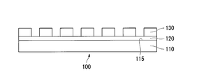
- FIG. 3 is a cross-sectional view showing the structure of the microwell array 100 according to the fifth embodiment.
- the hydrophilic layer 120 is formed on the surface 115 of the substrate 110.
- the substrate 110 may be a glass substrate, for example.
- the hydrophilic layer 120 may be, for example, a siloxane polymer formed from a silane coupling agent or a curable resin.
- the hydrophilic layer 120 is formed by applying the curable resin onto the substrate 110 and curing it by heat treatment or the like.
- a silane coupling agent may be added to the curable resin.
- the adhesion of the hydrophilic layer 120 to the substrate 110 is improved.
- a hydrophobic resin as a material for the hydrophobic layer 130 is applied on the hydrophilic layer 120.
- a photoresist may be used as the hydrophobic resin.
- a photoresist is applied on the hydrophilic layer 120 by spin coating or the like. After the spin coating, the photoresist is prebaked by applying heat and solidified to generate the hydrophobic layer 130.
- the hydrophobic layer 130 is excavated to form a well.
- the excavation can be performed by developing a photoresist, for example.
- a pattern mask is attached on the hydrophobic layer 130 and exposed to ultraviolet rays or the like to be exposed.
- the photoresist for example, a positive type photoresist is used.
- a positive type photoresist is decomposed when exposed to light and dissolved in a developer.
- a pattern mask having a design in which a hole of a target pattern is opened at a position where a microwell is to be formed is used as the pattern mask.
- the exposure time and conditions may be appropriately determined with reference to the photoresist data sheet to be used.
- the microwell array 100 is formed.
- the development time is appropriately determined with reference to the data sheet of the photoresist to be used.
- stop the development with a rinse solution and wash. For example, pure water or the like may be used as the rinse liquid.
- post-baking is performed to stabilize the photoresist.
- the microwell array 100 according to this embodiment can be manufactured.
- the bottom of the well of the microwell array is formed by the hydrophilic layer 120.
- a plurality of wells may be formed by excavating the hydrophobic layer 130 and the hydrophilic layer 120.
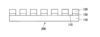
- FIG. 4 is a cross-sectional view showing the structure of a microwell array 200 according to the sixth embodiment.
- the microwell array 200 having wells where the surface 115 of the substrate 110 is exposed can be manufactured.
- the seventh embodiment of the present invention is a method for analyzing an aqueous liquid in which an aqueous liquid is enclosed, the wells of the microwell array according to the above embodiment are irradiated with electromagnetic waves, and fluorescence or phosphorescence emitted from the wells is detected. provide.
- the analysis method according to the present embodiment can measure how many of the wells constituting the microwell array emit fluorescence or phosphorescence. For example, by performing a PCR reaction in a microwell array and detecting fluorescence of SYBR Green in wells in which PCR amplification was observed, the proportion of wells in which amplification was observed can be calculated.
- the analysis method according to the present embodiment may be performed using, for example, a fluorescence microscope.
- the electromagnetic wave irradiation may be performed from the substrate side of the microwell array, from the well side, or from any other direction.
- Detection of fluorescence or phosphorescence generated as a result of irradiation with electromagnetic waves may be performed from the substrate side of the microwell array, may be performed from the well side, or may be performed from any other direction.
- detecting fluorescence or phosphorescence using a fluorescence microscope it is convenient to detect fluorescence or phosphorescence from the substrate side of the microwell array.
- Example 1 The microwell array of Example 1 was manufactured according to the manufacturing method of the fifth embodiment described above.
- the microwell array of Example 1 had a cylindrical well having a diameter of about 5 ⁇ m and a height of about 3 ⁇ m, and the bottom surface of the well was formed of a hydrophilic resin (hydrophilic layer).
- the well density was 1 million / cm 2 .
- a glass substrate was used as the substrate.
- a silane coupling agent model number “Z6094”, manufactured by Toray Dow Corning Co., Ltd., contact angle measured according to the sessile drop method defined in JIS R3257-1999: 55.3 degrees
- hydrophobic resin a positive photoresist (model number “S1818”, manufactured by Dow, contact angle measured according to the sessile drop method defined in JIS R3257-1999: 88.4 degrees) was used. Therefore, the wells of the microwell array of Example 1 have a hydrophobic portion near the well entrance on the well surface, and the hydrophilic portion is located closer to the bottom of the well (position closer to the bottom of the well) than the hydrophobic portion. And the well bottom was also hydrophilic.
- Example 2 The microwell array of Example 2 was produced according to the manufacturing method of the sixth embodiment described above.
- the microwell array of Example 2 had a cylindrical well having a diameter of about 5 ⁇ m and a height of about 3 ⁇ m.
- the well density was 1 million / cm 2 .
- a glass substrate contact angle measured according to the sessile drop method defined in JIS R3257-1999: 65.0 degrees
- hydrophilic resin a silane coupling agent (model number “Z6094”, manufactured by Toray Dow Corning Co., Ltd., contact angle measured according to the sessile drop method defined in JIS R3257-1999: 55.3 degrees) was used. .
- hydrophobic resin a positive photoresist (model number “S1818”, manufactured by Dow, contact angle measured according to the sessile drop method defined in JIS R3257-1999: 88.4 degrees) was used. Therefore, the wells of the microwell array of Example 2 have a hydrophobic portion near the well entrance on the well surface, and the hydrophilic portion is located closer to the bottom of the well (position closer to the bottom of the well) than the hydrophobic portion. Had.
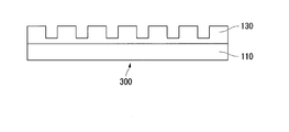
- FIG. 5 is a cross-sectional view showing the structure of the microwell array 300 of the first comparative example.
- the microwell array of Comparative Example 1 had a cylindrical well having a diameter of about 5 ⁇ m and a height of about 3 ⁇ m.
- a glass substrate was used as the substrate.
- a positive photoresist (model number “S1818”, manufactured by Dow, contact angle measured according to the sessile drop method defined in JIS R3257-1999: 88.4 degrees) was used. As shown in FIG.
- the microwell array 300 has a structure in which the hydrophobic layer 130 is directly laminated on the substrate 110, and the well is formed inside the hydrophobic layer 130. Therefore, the wells of the microwell array of Comparative Example 1 all had well surfaces formed from hydrophobic portions.
- Example 1 A microfluidic device comprising the microwell array of Example 1 was assembled. Subsequently, an aqueous solution in which a proper amount of FITC (fluorescein isothiocyanate), which is a fluorescent substance, and a surfactant were dissolved was sent to the microfluidic device using a syringe. Thereafter, oil (model number “FC40”, manufactured by Sigma, contact angle of 7.0 ° with respect to positive photoresist (model number “S1818”)) was sent to the microfluidic device using a syringe.
- FITC fluorescein isothiocyanate
- S1818 contact angle of 7.0 ° with respect to positive photoresist
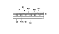
- FIG. 6 is a cross-sectional view showing a state after oil is fed to the microfluidic device of this experimental example.
- the microfluidic device 400 was provided with a bottom member 410 that holds a microwell array, a lid member 420, and a microchannel 430.
- the bottom member 410 was integrated with the substrate 110 of the microwell array 100 of Example 1. That is, the microwell array 100 of Example 1 was formed using the bottom member 410 as the substrate 110.
- the aqueous liquid 440 (an aqueous solution in which an appropriate amount of FITC and a surfactant was dissolved) was sent to the microfluidic device 400 from the channel inlet (not shown), the aqueous liquid 440 was introduced into the wells of the microwell array 100. Subsequently, when the oil 450 is supplied to the microfluidic device 400 from a channel inlet (not shown), a layer of the oil 450 is formed near the well inlet of the well while the aqueous liquid 440 is held in the well of the microwell array 100. Been formed. That is, the aqueous liquid 440 was sealed in the wells of the microwell array 100. Each well functions as a chemical reaction vessel that performs various biochemical or chemical reactions in a small volume of aqueous liquid 440.
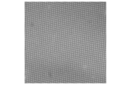
- FIG. 7 is a photograph showing the result of fluorescence microscopic observation of the microwell array of Example 1 from the substrate side (on the substrate, the bottom of the microfluidic device) after the oil was fed.
- FITC-derived fluorescence was regularly observed in the well pattern of the microwell array of Example 1.
- the white portion is a fluorescent well
- the black portion is a substrate. This result shows that the FITC solution could be encapsulated in each well of the microwell array of Example 1.
- Example 2 As a microwell array, FITC and a surfactant were dissolved in appropriate amounts in the microwell array in the same manner as in Experimental Example 1, except that the microwell array of Example 2 was used instead of the microwell array of Example 1. An aqueous solution was enclosed.
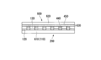
- FIG. 8 is a cross-sectional view showing a state after oil is fed to the microfluidic device of this experimental example.
- the microfluidic device 600 includes a bottom member 610 that holds a microwell array, a lid member 620, and a microchannel 630.
- the bottom member 610 was integrated with the substrate 110 of the microwell array 200 of Example 2. That is, the microwell array 200 of Example 2 was formed using the bottom member 610 as the substrate 110.
- aqueous liquid 440 an aqueous solution in which an appropriate amount of FITC and a surfactant was dissolved
- the aqueous liquid 440 was introduced into the wells of the microwell array 200.
- the oil 450 is supplied to the microfluidic device 600 from a channel inlet (not shown)
- a layer of the oil 450 is formed near the well inlet of the well while the aqueous liquid 440 is held in the well of the microwell array 200. Been formed. That is, the aqueous liquid 440 was sealed in the wells of the microwell array 200.
- FIG. 9 is a photograph showing a result of observing the microwell array of Example 2 from the substrate side with a fluorescence microscope after feeding the oil. As a result, as shown in FIG. 9, FITC fluorescence was regularly observed in the well pattern of the microwell array of Example 2. In FIG. 9, the white portion is a well emitting fluorescence, and the black portion is a substrate. This result shows that the FITC solution could be encapsulated in each well of the microwell array of Example 2.
- the novolak resin used as the hydrophobic resin has autofluorescence, but the fluorescence value of the novolac resin is sufficiently low, and is the detection value and the fluorescence value of the novolac resin. Since there was a sufficient difference from the fluorescence value of FITC, there was no problem in the detection of FITC fluorescence.
- Example 3 As a microwell array, FITC and a surfactant were dissolved in appropriate amounts in the same manner as in Experimental Example 1, except that the microwell array of Comparative Example 1 was used instead of the microwell array of Example 1. An aqueous solution was enclosed.
- FIG. 10 is a cross-sectional view showing a state after oil is fed to the microfluidic device of this experimental example.
- the microfluidic device 700 was provided with a bottom member 710 for holding a microwell array, a lid member 720, and a microchannel 730.
- the bottom member 710 was formed integrally with the substrate 110 of the microwell array 300 of Comparative Example 1. That is, the microwell array 300 of Comparative Example 1 was formed using the bottom member 710 as the substrate 110.
- aqueous liquid 440 an aqueous solution in which an appropriate amount of FITC and a surfactant is dissolved
- the oil 450 is fed from an unillustrated channel inlet
- Liquid 440 could not be retained in the wells of microwell array 300. That is, in the microwell array 300 of Comparative Example 1, it was difficult to enclose the aqueous liquid 440 in the well.
- FIG. 11 is a photograph showing a result of observing the microwell array of Comparative Example 1 from the substrate side with a fluorescence microscope after feeding the oil.
- fluorescence was observed across a plurality of wells, and regular FITC fluorescence along the well pattern was not observed.
- This result shows that the FITC solution could not be encapsulated in the microwell array of Comparative Example 1. That is, when the microwell is formed only by the hydrophobic layer, it becomes difficult to hold the aqueous solution, and when the oil is fed, it becomes clear that all the aqueous solution in the well is replaced with the oil. It was.
- a microwell array in which an aqueous liquid can be easily enclosed in a well.
- the manufacturing method of said microwell array, a microfluidic device, the method of enclosing aqueous liquid in the well of a microwell array, and the analysis method of aqueous liquid can be provided.
- diagnosis is performed by detecting DNA or RNA derived from a living body, a nucleic acid can be put together with a reagent into a minute space.
Landscapes
- Chemical & Material Sciences (AREA)
- Health & Medical Sciences (AREA)
- Engineering & Computer Science (AREA)
- Life Sciences & Earth Sciences (AREA)
- Analytical Chemistry (AREA)
- General Health & Medical Sciences (AREA)
- Biochemistry (AREA)
- Organic Chemistry (AREA)
- Bioinformatics & Cheminformatics (AREA)
- Physics & Mathematics (AREA)
- General Physics & Mathematics (AREA)
- Immunology (AREA)
- Pathology (AREA)
- Wood Science & Technology (AREA)
- Biotechnology (AREA)
- Zoology (AREA)
- Microelectronics & Electronic Packaging (AREA)
- Sustainable Development (AREA)
- Manufacturing & Machinery (AREA)
- Medicinal Chemistry (AREA)
- Biomedical Technology (AREA)
- Microbiology (AREA)
- Computer Hardware Design (AREA)
- Nuclear Medicine, Radiotherapy & Molecular Imaging (AREA)
- Chemical Kinetics & Catalysis (AREA)
- General Engineering & Computer Science (AREA)
- Genetics & Genomics (AREA)
- Apparatus Associated With Microorganisms And Enzymes (AREA)
- Investigating, Analyzing Materials By Fluorescence Or Luminescence (AREA)
- Automatic Analysis And Handling Materials Therefor (AREA)
Abstract
マイクロウェルアレイであって、ウェル表面に親水性部分及び疎水性部分を有する複数のウェルを備える。
Description
本発明は、マイクロウェルアレイ及びその製造方法、マイクロ流体デバイス、マイクロウェルアレイのウェル内に水性液体を封入する方法及び水性液体の分析方法に関する。
本願は、2015年3月30日に日本に出願された特願2015-067960号に基づき優先権を主張し、その内容をここに援用する。
本願は、2015年3月30日に日本に出願された特願2015-067960号に基づき優先権を主張し、その内容をここに援用する。
近年、半導体回路の製造技術に用いられているエッチング技術やフォトリソグラフィ技術等を用いて形成された、種々の形態の微細な流路構造を有するマイクロウェルアレイが検討されている。これらのマイクロウェルアレイのウェルは、微小体積の流体中で種々の生化学的又は化学的反応をさせるための化学反応容器として用いられている。
マイクロ流体システムの製作のための材料としては、シリコン、ガラス等の硬質の物質、PDMS(ポリジメチルシロキサン)等の種々の高分子樹脂やシリコーンゴム等の軟質の物質等が用いられている。例えば、特許文献1~4には、このようなマイクロ流体システムを、種々のマイクロチップ、バイオチップとして用いることが記載されている。
ところで、近年、微少量の容積を有する微小空間内で酵素反応を行うことにより生体物質の検査を行う技術が注目されている。例えば、核酸の検出及び定量における新しいアプローチの一つとして、デジタルPCR技術が挙げられる。デジタルPCR技術とは、試薬と核酸との混合物を無数の微小液滴に分割してPCR増幅を行い、核酸を含んだ液滴からは蛍光等のシグナルが検出されるようにしておき、シグナルが検出された液滴を数えることにより定量を行う技術である。
微小液滴の作製方法として、封止液で分断化することにより微小液滴を作製する方法や、基板上に形成した孔に試薬を入れ、続いて封止液を入れることにより微小液滴を作製する方法(例えば特許文献4を参照。)等が検討されている。
しかしながら、従来のマイクロウェルアレイは、水性液体であるPCR反応液等の試料をウェル内に封入することが困難な場合がある。
そこで、本発明は、ウェル内に水性液体を封入することが容易なマイクロウェルアレイを提供することを目的とする。本発明はまた、上記のマイクロウェルアレイの製造方法、マイクロ流体デバイス、マイクロウェルアレイのウェル内に水性液体を封入する方法及び水性液体の分析方法を提供することを目的とする。
本発明の第一態様に係るマイクロウェルアレイは、ウェル表面に親水性部分及び疎水性部分を有する複数のウェルを備える。
前記複数のウェルのうちそれぞれのウェルの容量が1fL~6nLであってもよい。
前記複数のウェルの密度が10万~1000万個/cm2であってもよい。
前記複数のウェルは、ウェル上部に前記疎水性部分を有し、前記疎水性部分よりもウェル底部に近い位置に前記親水性部分を有していてもよい。
前記複数のウェルが、電磁波に対し透過性を有する基板上に設けられていてもよい。
前記電磁波が、X線、紫外線、可視光線又は赤外線であってもよい。
前記基板は、自家蛍光を実質的に有しない材料で形成されていてもよい。
前記親水性部分はJIS R3257-1999に規定された静滴法に準じて測定した接触角が70度未満であってもよい。
前記親水性部分がシロキサンポリマーで形成されていてもよい。
前記疎水性部分はJIS R3257-1999に規定された静滴法に準じて測定した接触角が70度以上であってもよい。
前記疎水性部分がノボラック樹脂で形成されていてもよい。
本発明の第二態様に係るマイクロ流体デバイスは、流路と、前記流路内に配置された上記態様に係るマイクロウェルアレイとを備える。
本発明の第三態様に係るウェル内に水性液体を封入する方法は、流路と、前記流路内に配置された上記態様に係るマイクロウェルアレイとを備えるマイクロ流体デバイスを準備し、前記マイクロ流体デバイスの前記流路に水性液体を送液し、前記マイクロウェルアレイのウェルに前記水性液体を導入し、前記流路に封止液を送液し、前記ウェルに導入された前記水性液体の上層に封止液の層を形成させ、前記水性液体を前記ウェル内に封入する。
本発明の第四態様に係るマイクロウェルアレイの製造方法は、電磁波透過性を有する基板上に親水性材料を積層して親水層を形成し、前記親水層上に疎水性材料を積層して疎水層を形成し、前記疎水層を掘削して複数のウェルを形成する。
前記複数のウェルを形成する際に、前記疎水層及び前記親水層を掘削して複数のウェルを形成してもよい。
本発明の第五態様に係る水性液体の分析方法は、水性液体が封入された、上記態様に係るマイクロウェルアレイのウェルに電磁波を照射し、前記ウェルから放出される蛍光又は燐光を検出する。
前記蛍光又は前記燐光が、上記態様に係るマイクロウェルアレイの基板上で検出されてもよい。
本発明の上記態様によれば、ウェル内に水性液体を封入することが容易なマイクロウェルアレイを提供することができる。また、上記態様に係るマイクロウェルアレイの製造方法、マイクロ流体デバイス、マイクロウェルアレイのウェル内に水性液体を封入する方法、及び水性液体の分析方法を提供することができる。
以下、場合により図面を参照しつつ、本発明の実施形態について詳細に説明する。なお、図面中、同一又は相当部分には同一符号を付し、重複する説明は省略する。なお、各図における寸法比は、説明のため誇張している部分があり、必ずしも実際の寸法比とは一致しない。
[マイクロウェルアレイ]
本発明の第1実施形態は、ウェル表面に親水性部分及び疎水性部分を有する複数のウェルを備える、マイクロウェルアレイを提供する。後述するように、本実施形態に係るマイクロウェルアレイは、ウェル内に水性液体を封入することが非常に容易である。ここで、水性液体を封入するとは、マイクロウェルアレイを構成する複数のウェルに水性液体を導入し、更に、各ウェルに導入された液体同士が互いに混合しない状態に隔離することを意味する。隔離する方法としては、例えば、ウェルに水性液体を導入した後、ウェルの上部にオイル層を形成すること等が挙げられる。本実施形態に係るマイクロウェルアレイによれば、マイクロウェルアレイを構成する複数のウェルの90%以上、例えば95%以上、例えば99%以上、例えば100%に水性液体を容易に封入することができる。
本発明の第1実施形態は、ウェル表面に親水性部分及び疎水性部分を有する複数のウェルを備える、マイクロウェルアレイを提供する。後述するように、本実施形態に係るマイクロウェルアレイは、ウェル内に水性液体を封入することが非常に容易である。ここで、水性液体を封入するとは、マイクロウェルアレイを構成する複数のウェルに水性液体を導入し、更に、各ウェルに導入された液体同士が互いに混合しない状態に隔離することを意味する。隔離する方法としては、例えば、ウェルに水性液体を導入した後、ウェルの上部にオイル層を形成すること等が挙げられる。本実施形態に係るマイクロウェルアレイによれば、マイクロウェルアレイを構成する複数のウェルの90%以上、例えば95%以上、例えば99%以上、例えば100%に水性液体を容易に封入することができる。
本実施形態に係るマイクロウェルアレイは、ウェル1つあたりの容量が、例えば1フェムトリットル(fL)~6ナノリットル(nL)であり、好ましくは1fL~5ピコリットル(pL)であり、更に好ましくは1fL~300fLである。ウェル1つあたりの容量がこのような範囲(1fL~6nL)であると、デジタルPCRやインベーダー反応等の微小空間内で行う酵素反応を好適に行うことができる。また、当該デジタルPCRにより、例えば遺伝子の変異検出等を行うことができる。
例えば、セルフリーDNAの変異を測定する場合において、検出対象の遺伝子を含んだサンプル量が決まっている際は、ウェル数が同じ場合でも反応容積がより小さいほうが好ましい。
例えば、セルフリーDNAの変異を測定する場合において、検出対象の遺伝子を含んだサンプル量が決まっている際は、ウェル数が同じ場合でも反応容積がより小さいほうが好ましい。
マイクロウェルアレイを用いた解析に酵素反応を利用する場合には、マイクロウェルアレイの材質が酵素反応を阻害しない材質であることが好ましい。あるいは、マイクロウェルアレイの材質(材料)表面に、酵素反応を阻害しない物質をコーティングすることも可能である。
マイクロウェルアレイのウェルの形状や大きさに特に制限はないが、例えば、微小液滴中で種々の生化学的な反応を行う場合には、1~数個の生体分子又は担体を収容可能な形状と大きさを有していることが好ましい。担体は例えばビーズであってもよく、担体には試料である生体分子が結合されていてもよい。
ウェルの形状は、例えば、円筒形、複数の面により構成される多面体(例えば、直方体、六角柱、八角柱等)、逆円錐形、逆角錐形(逆三角錐形、逆四角錐形、逆五角錐形、逆六角錐形、七角以上の逆多角錐形)等であってもよく、これらの形状の二つ以上を組み合わせた形状であってもよい。
例えば、一部が円筒形であり、残りが逆円錐形であってもよい。また、逆円錐形、逆角錐形の場合、円錐や角錐の底面がウェルの入り口(開口部)となるが、逆円錐形、逆角錐形の頂上から一部を切り取った形状であってもよい。この場合、マイクロウェルの底部は平坦になる。
ウェルの形状が円筒形、直方体である場合、マイクロウェルの底部は通常、平坦であるが、曲面(凸面や凹面)としてもよい。マイクロウェルの底部を曲面とすることができるのは、逆円錐形、逆角錐形の頂上から一部を切り取った形状の場合も同様である。
ウェルが円筒形の場合、生体分子を含む水性液体を封入する目的のためには、直径は3~10μmであってもよい。また、深さは3~10μmであってもよい。ウェルの寸法は、ウェルに収容する水性液体の量や、生体分子を付着させたビーズ等の担体の大きさとウェルの寸法の好適な比等を考慮して、1つのマイクロウェルに1つ、もしくは数個の生体分子が収容されるように、適宜決定する。
本実施形態に係るマイクロウェルアレイを使用して検出する検出対象は、例えば血液等の生体から採取した試料やPCR産物等であってもよく、人工的に合成された化合物等であってもよい。例えば、生体分子であるDNAを検出対象とする場合、ウェルは、DNAが1分子入るような形状と大きさであってもよい。
生体分子のほかの例として、タンパク質やRNA(miRNA、mtRNA、tRNAなどのRNAを含む)、糖、アミノ酸(ペプチドを含む)が挙げられる。
生体分子のほかの例として、タンパク質やRNA(miRNA、mtRNA、tRNAなどのRNAを含む)、糖、アミノ酸(ペプチドを含む)が挙げられる。
本実施形態に係るマイクロウェルアレイにおいては、複数のウェルの密度が、例えば10万~1000万個/cm2であり、好ましくは10万~500万個/cm2であり、更に好ましくは10万~100万個/cm2である。ウェルの密度がこのような範囲(10万~1000万個/cm2)であると、所定数のウェルに試料である水性液体を封入させる操作が容易である。また、実験結果を解析するためのウェルの観察も容易である。
例えば、前記容積でウェルを作製した場合、顕微鏡でウェルを観察する際は、1視野で取得できるウェル数は1万個程度となる。セルフリーDNAの変異を測定する場合において、検出対象の変異の野生型に対する存在割合が0.01%程度である場合、10万~500万個/cm2程度、更に好ましくは10万~100万個/cm2あると、検出精度を損なわずに全ウェルを検出したとしても迅速な測定が可能となる。
例えば、前記容積でウェルを作製した場合、顕微鏡でウェルを観察する際は、1視野で取得できるウェル数は1万個程度となる。セルフリーDNAの変異を測定する場合において、検出対象の変異の野生型に対する存在割合が0.01%程度である場合、10万~500万個/cm2程度、更に好ましくは10万~100万個/cm2あると、検出精度を損なわずに全ウェルを検出したとしても迅速な測定が可能となる。
例えば、セルフリーDNAの変異を測定する場合において、検出対象の変異の野生型に対する存在割合が0.01%程度である場合、例えば、100万~200万個のウェルを使用することが好適である。
本実施形態に係るマイクロウェルアレイにおいて、(複数のウェルのうち)各ウェルは、ウェル上部に前記疎水性部分を有し、前記疎水性部分よりもウェル底部に近い位置(底側)に前記親水性部分を有することが好ましい。
後述するように、発明者らは、このような構成とすることにより、マイクロウェルアレイのウェルに水性液体を封入させることが非常に容易になることを見出した。
後述するように、発明者らは、このような構成とすることにより、マイクロウェルアレイのウェルに水性液体を封入させることが非常に容易になることを見出した。
上記の親水性部分(親水性部分の材質)は、JIS R3257-1999に規定された静滴法に準じて測定した接触角が70度未満であってよい。いいかえると、本明細書において、親水性であるとは、JIS R3257-1999に規定された静滴法に準じて測定した接触角が70度未満であることを意味する。
また、上記の疎水性部分(疎水性部分の材質)は、JIS R3257-1999に規定された静滴法に準じて測定した接触角が70度以上であってよい。いいかえると、本明細書において、疎水性であるとは、JIS R3257-1999に規定された静滴法に準じて測定した接触角が70度以上であることを意味する。
(親水性樹脂)
親水性部分を形成する樹脂(以下「親水性樹脂」という場合がある。)としては、本発明の効果を奏する限り特に限定されないが、樹脂の構成成分の分子が、親水性を発現する親水性基を有する樹脂が挙げられる。親水性基としては、例えば、ヒドロキシル基、カルボキシル基、スルホン基、スルホニル基、アミノ基、アミド基、エーテル基、エステル基等が挙げられる。
親水性部分を形成する樹脂(以下「親水性樹脂」という場合がある。)としては、本発明の効果を奏する限り特に限定されないが、樹脂の構成成分の分子が、親水性を発現する親水性基を有する樹脂が挙げられる。親水性基としては、例えば、ヒドロキシル基、カルボキシル基、スルホン基、スルホニル基、アミノ基、アミド基、エーテル基、エステル基等が挙げられる。
より具体的には、シロキサンポリマー;エポキシ樹脂;ポリエチレン樹脂;ポリエステル樹脂;ポリウレタン樹脂;ポリアクリルアミド樹脂;ポリビニルピロリドン樹脂;ポリアクリル酸共重合体等のアクリル樹脂;カチオン化ポリビニルアルコール、シラノール化ポリビニルアルコール、スルホン化ポリビニルアルコール等のポリビニルアルコール樹脂;ポリビニルアセタール樹脂;ポリビニルブチラール樹脂;ポリエチレンポリアミド樹脂;ポリアミドポリアミン樹脂;ヒドロキシメチルセルロース、メチルセルロース等のセルロース誘導体;ポリエチレンオキサイド、ポリエチレンオキサイド-ポリプロピレンオキサイド共重合体等のポリアルキレンオキサイド誘導体;無水マレイン酸共重合体;エチレン-酢酸ビニル共重合体;スチレン-ブタジエン共重合体;上記の樹脂の組み合わせ等の中から、JIS R3257-1999に規定された静滴法に準じて測定した接触角が70度未満である樹脂を少なくとも1つ以上適宜選択して使用することができる。
すなわち、親水性樹脂としては、上記樹脂のうち接触角が70度未満である樹脂であれば、1種類の樹脂のみを用いてもよく、複数種類の樹脂を組み合わせて用いてもよい。
親水性樹脂は、熱可塑性樹脂であってもよく、熱硬化性樹脂であってもよく、電子線やUV光等の活性エネルギー線により硬化する樹脂であってもよく、エラストマーであってもよい。
すなわち、親水性樹脂としては、上記樹脂のうち接触角が70度未満である樹脂であれば、1種類の樹脂のみを用いてもよく、複数種類の樹脂を組み合わせて用いてもよい。
親水性樹脂は、熱可塑性樹脂であってもよく、熱硬化性樹脂であってもよく、電子線やUV光等の活性エネルギー線により硬化する樹脂であってもよく、エラストマーであってもよい。
また、親水層は、後述する基板が存在する場合には、基板と疎水層とを密着させる機能も有していてもよい。例えば、熱硬化性のシランカップリング剤等を基板に塗布し、熱硬化させてシロキサンポリマーを形成することにより、親水層を形成してもよい。
(疎水性樹脂)
疎水性部分を形成する樹脂(以下「疎水性樹脂」という場合がある。)としては、本発明の効果を奏する限り特に限定されないが、例えば、ノボラック樹脂;アクリル樹脂;メタクリル樹脂;スチレン樹脂;塩化ビニル樹脂;塩化ビニリデン樹脂;ポリオレフィン樹脂;ポリアミド樹脂;ポリイミド樹脂;ポリアセタール樹脂;ポリカーボネート樹脂;ポリフェニレンスルフィド樹脂;ポリスルフォン樹脂;フッ素樹脂;シリコーン樹脂;ユリヤ樹脂;メラミン樹脂;グアナミン樹脂;フェノール樹脂;セルロース樹脂;上記の樹脂の組み合わせ等の中から、JIS R3257-1999に規定された静滴法に準じて測定した接触角が70度以上である樹脂を少なくとも1つ以上適宜選択して使用することができる。
すなわち、疎水性樹脂としては、上記樹脂のうち接触角が70度以上である樹脂であれば、1種類の樹脂のみを用いてもよく、複数種類の樹脂を組み合わせて用いてもよい。
疎水性樹脂は、熱可塑性樹脂であってもよく、熱硬化性樹脂であってもよく、電子線やUV光等の活性エネルギー線により硬化する樹脂であってもよく、エラストマーであってもよい。
疎水性部分を形成する樹脂(以下「疎水性樹脂」という場合がある。)としては、本発明の効果を奏する限り特に限定されないが、例えば、ノボラック樹脂;アクリル樹脂;メタクリル樹脂;スチレン樹脂;塩化ビニル樹脂;塩化ビニリデン樹脂;ポリオレフィン樹脂;ポリアミド樹脂;ポリイミド樹脂;ポリアセタール樹脂;ポリカーボネート樹脂;ポリフェニレンスルフィド樹脂;ポリスルフォン樹脂;フッ素樹脂;シリコーン樹脂;ユリヤ樹脂;メラミン樹脂;グアナミン樹脂;フェノール樹脂;セルロース樹脂;上記の樹脂の組み合わせ等の中から、JIS R3257-1999に規定された静滴法に準じて測定した接触角が70度以上である樹脂を少なくとも1つ以上適宜選択して使用することができる。
すなわち、疎水性樹脂としては、上記樹脂のうち接触角が70度以上である樹脂であれば、1種類の樹脂のみを用いてもよく、複数種類の樹脂を組み合わせて用いてもよい。
疎水性樹脂は、熱可塑性樹脂であってもよく、熱硬化性樹脂であってもよく、電子線やUV光等の活性エネルギー線により硬化する樹脂であってもよく、エラストマーであってもよい。
疎水性部分は、例えばレジストで形成されていてもよい。レジストは、微細構造を形成しやすい観点から、フォトレジストであってもよい。フォトレジストは、例えば、感光性のノボラック樹脂であってもよい。
(基板)
本実施形態に係るマイクロウェルアレイは、基板上に形成されていてもよい。基板は、電磁波透過性を有する基板であってもよく、電磁波透過性を有しない基板であってもよい。ここで、電磁波としては、X線、紫外線、可視光線、赤外線等が挙げられる。マイクロウェルアレイが電磁波透過性を有する基板上に形成されていた場合には、マイクロウェルアレイ上で行った実験結果を解析するために、電磁波を利用することが可能になる。例えば、電磁波を照射した結果生じる蛍光、燐光等を基板側から(基板を介して、基板上で)計測することができる。本明細書において、蛍光及び燐光は、照射時と検出時の波長が異なる(波長が変換される)光も含む。波長が変換される例としては、紫外線を照射した結果、可視光領域の蛍光又は燐光が発生する場合、可視光線を照射した結果、赤外領域の蛍光又は燐光が発生する場合等が挙げられる。蛍光、燐光等の検出には、例えば蛍光顕微鏡等を利用することができる。この場合、電磁波は、例えば基板側から(基板に対して)照射してもよいし、例えばウェルの入り口側から(ウェルの入り口に対して)照射してもよい。
本実施形態に係るマイクロウェルアレイは、基板上に形成されていてもよい。基板は、電磁波透過性を有する基板であってもよく、電磁波透過性を有しない基板であってもよい。ここで、電磁波としては、X線、紫外線、可視光線、赤外線等が挙げられる。マイクロウェルアレイが電磁波透過性を有する基板上に形成されていた場合には、マイクロウェルアレイ上で行った実験結果を解析するために、電磁波を利用することが可能になる。例えば、電磁波を照射した結果生じる蛍光、燐光等を基板側から(基板を介して、基板上で)計測することができる。本明細書において、蛍光及び燐光は、照射時と検出時の波長が異なる(波長が変換される)光も含む。波長が変換される例としては、紫外線を照射した結果、可視光領域の蛍光又は燐光が発生する場合、可視光線を照射した結果、赤外領域の蛍光又は燐光が発生する場合等が挙げられる。蛍光、燐光等の検出には、例えば蛍光顕微鏡等を利用することができる。この場合、電磁波は、例えば基板側から(基板に対して)照射してもよいし、例えばウェルの入り口側から(ウェルの入り口に対して)照射してもよい。
例えば、マイクロウェルアレイにおいて、可視光領域である400~700nmの波長範囲にピークを有する蛍光を検出する場合には、少なくとも上記可視光領域の光に対して良好な透過性を有する基板を用いればよい。
電磁波透過性を有する基板としては、例えば、ガラス、樹脂等が挙げられる。樹脂基板としては、例えば、ABS樹脂、ポリカーボネート樹脂、COC(シクロオレフィンコポリマー)、COP(シクロオレフィンポリマー)、アクリル樹脂、ポリ塩化ビニル、ポリスチレン樹脂、ポリエチレン樹脂、ポリプロピレン樹脂、ポリ酢酸ビニル、PET(ポリエチレンテレフタレート)、PEN(ポリエチレンナフタレート)等が挙げられる。これらの樹脂は各種添加剤を含んでいてもよく、複数の樹脂が混合されていてもよい。
実験結果の検出に蛍光や燐光を利用する観点から、上記の基板は、自家蛍光を実質的に有しないことが好ましい。ここで、自家蛍光を実質的に有しないとは、基板が、実験結果の検出に使用する波長の自家蛍光を全く有しないか、自家蛍光を有していても実験結果の検出に影響を与えないほど微弱であることを意味する。例えば、検出対象の蛍光に比べて1/10以下、1/100以下程度の自家蛍光であれば、実験結果の検出に影響を与えないほど微弱であるといえる。
電磁波透過性を有し、かつ自家蛍光を全く発しない素材としては、例えば、石英ガラスが挙げられる。自家蛍光が微弱であり、電磁波を用いた実験結果の検出に支障がない素材としては、低蛍光ガラス、アクリル樹脂、COC(シクロオレフィンコポリマー)、COP(シクロオレフィンポリマー)等が挙げられる。
生体分子の検出に用いる蛍光としては、例えば蛍光分子(蛍光物質)を内包した蛍光ビーズや、DNAの二重らせんに特異的に入り込み、蛍光を発するSYBR Green等のインターカレーター等に由来する蛍光が挙げられる。
その他に、蛍光色素などの蛍光物質、FRET(蛍光共鳴エネルギー移動)、蛍光標識をつけたアビジンやストレプトアビジンの反応や、ホースラディッシュペルオキシダーゼを用いた酵素反応、インベーダー(登録商標)法のようなFRETと酵素反応を組合わせた方法に由来する蛍光が挙げられる。
その他に、蛍光色素などの蛍光物質、FRET(蛍光共鳴エネルギー移動)、蛍光標識をつけたアビジンやストレプトアビジンの反応や、ホースラディッシュペルオキシダーゼを用いた酵素反応、インベーダー(登録商標)法のようなFRETと酵素反応を組合わせた方法に由来する蛍光が挙げられる。
ウェルに収容された生体分子から発せられる蛍光の観察は、例えば、倒立顕微鏡を用いて、マイクロウェルアレイの基板側から(基板を介して、基板上から)行うことができる。この蛍光観察により、所定の蛍光を発するマイクロウェルの個数を数えることで、目的分子の数を特定することができる。
生体分子は、例えば、ウェルに収容する前に、目的分子を特異的に標識する蛍光標識で処理しておくとよい。あるいは、対象分子を特異的に認識するビーズを用いて、対象分子を補足した後に、ビーズをウェルに収容し、対象分子を特異的に標識し得る蛍光標識と接触させて、目的分子をウェル内で蛍光標識してもよい。
基板の厚みは、適宜決定することが出来るが、例えば基板側(基板上)から蛍光顕微鏡を用いて蛍光を観察する場合には、例えば5mm以下、例えば2mm以下、例えば1.6mm以下であることが好ましい。
本実施形態に係るマイクロウェルアレイを使用した生体分子の観察には、蛍光以外にも、例えば濁度等を利用することもできる。濁度は、例えば、検出対象における400~1000nm程度の波長の光の透過性により測定することができる。
[マイクロ流体デバイス]
本発明の一実施形態は、流路と、前記流路内に配置された上記のマイクロウェルアレイとを備える、マイクロ流体デバイスを提供する。このようなマイクロ流体デバイスを用いることにより、マイクロウェルアレイのウェル内に水性液体を封入することが容易になる。
本発明の一実施形態は、流路と、前記流路内に配置された上記のマイクロウェルアレイとを備える、マイクロ流体デバイスを提供する。このようなマイクロ流体デバイスを用いることにより、マイクロウェルアレイのウェル内に水性液体を封入することが容易になる。
(第2実施形態)
図1Aは、第2実施形態に係るマイクロ流体デバイスを示す斜視図である。図1Bは、図1Aのマイクロ流体デバイスにおけるb-b線断面図である。図1Cは、図1Aのマイクロ流体デバイスにおけるc-c線断面図である。
図1Aは、第2実施形態に係るマイクロ流体デバイスを示す斜視図である。図1Bは、図1Aのマイクロ流体デバイスにおけるb-b線断面図である。図1Cは、図1Aのマイクロ流体デバイスにおけるc-c線断面図である。
本実施形態に係るマイクロ流体デバイス1000は、底部部材1100と、蓋部材1200と、流路1300と、流路1300の一端(第1端)に設けられた流路入口1210と、流路1300の他端(第2端)に設けられた流路出口1220と、流路1300の内壁の一部を形成する封止部材1400と、流路1300の内部に配置されたマイクロウェルアレイmとを備える。流路1300に流体を送液する場合には、例えば、シリンジ等を用いて、流路入口1210から流体を導入し、流路出口1220から排出するとよい。本実施形態に係るマイクロ流体デバイスでは、流路1300の内部にマイクロウェルアレイmが設けられている。
マイクロウェルアレイmの構造については後述する。マイクロウェルアレイmの基板1100と、マイクロ流体デバイス1000の底部部材1100は一体であってもよい。また、マイクロウェルアレイmの親水層1120及び疎水層1130は、マイクロ流体デバイス1000の底部部材1100上に一体成型されていてもよい。すなわち、マイクロウェルアレイmは、マイクロ流体デバイス1000の底部部材1100上に形成されていてもよい。
底部部材1100及び蓋部材1200の材質としては、上述したマイクロウェルアレイの基板の材質と同様の材質を使用することができる。また、封止部材1400の材質としては、特に制限されないが、例えばシリコーンゴム、アクリル発泡体から形成される芯材フィルムの両面にアクリル系粘着剤が積層された両面粘着テープ、接着剤を積層するなどして一定の厚みを有するもの、スペーサ部材(樹脂製、金属製、紙製、ガラス等の無機物)等が挙げられる。
これら封止部材は、送液される液体と反応しにくいものを適宜選択できる。また、封止部材の表面に、送液される液体と反応しにくくなるように、コーティングをしたものも採用できる。
本願では両面粘着テープを使用した。
これら封止部材は、送液される液体と反応しにくいものを適宜選択できる。また、封止部材の表面に、送液される液体と反応しにくくなるように、コーティングをしたものも採用できる。
本願では両面粘着テープを使用した。
(第3実施形態)
図2Aは、本発明の第3実施形態に係るマイクロ流体デバイスを示す斜視図である。図2Bは、図2Aのマイクロ流体デバイスにおけるb-b線断面図である。図2Cは、図2Aのマイクロ流体デバイスにおけるc-c線断面図である。
図2Aは、本発明の第3実施形態に係るマイクロ流体デバイスを示す斜視図である。図2Bは、図2Aのマイクロ流体デバイスにおけるb-b線断面図である。図2Cは、図2Aのマイクロ流体デバイスにおけるc-c線断面図である。
本実施形態に係るマイクロ流体デバイス2000は、上述した第1実施形態に係るマイクロ流体デバイス1000の平面視において、流路1300の一部が拡大された構成を有する。また、マイクロ流体デバイス2000におけるマイクロウェルアレイm(第2のマイクロウェルアレイm-2)は、マイクロ流体デバイス1000におけるマイクロウェルアレイmと比較して、平面視における面積が大きくなっている。マイクロ流体デバイス2000のその他の構成(第2のマイクロウェルアレイm-2以外の構成)においてはマイクロ流体デバイス1000と同様である。
なお、本明細書において平面視とは、マイクロ流体デバイスの底部部材又はマイクロウェルアレイの基板に対して垂直な方向からマイクロ流体デバイス又はマイクロウェルアレイを見た状態をいう。
[マイクロウェルアレイのウェル内に水性液体を封入する方法]
本発明の第4実施形態は、流路と、前記流路内に配置された上記の実施形態に係るマイクロウェルアレイとを備えるマイクロ流体デバイスを準備し、前記マイクロ流体デバイスの前記流路に水性液体を送液し、前記マイクロウェルアレイのウェルに前記水性液体を導入し、前記流路に封止液を送液し、前記ウェルに導入された前記水性液体の上層に封止液の層を形成させ、前記水性液体を前記ウェル内に封入する、マイクロウェルアレイのウェル内に水性液体を封入する方法を提供する。
本発明の第4実施形態は、流路と、前記流路内に配置された上記の実施形態に係るマイクロウェルアレイとを備えるマイクロ流体デバイスを準備し、前記マイクロ流体デバイスの前記流路に水性液体を送液し、前記マイクロウェルアレイのウェルに前記水性液体を導入し、前記流路に封止液を送液し、前記ウェルに導入された前記水性液体の上層に封止液の層を形成させ、前記水性液体を前記ウェル内に封入する、マイクロウェルアレイのウェル内に水性液体を封入する方法を提供する。
ここで、水性液体とは、水、検出対象である生体分子を含有する緩衝液等の生体試料、酵素反応液等を意味する。生体試料は一般的に水性液体である。水性液体は、例えば、生体試料を鋳型とし、検出試薬としてSYBR Greenを含むPCR反応溶液等であってもよい。また、水性液体中には、界面活性剤等の添加物を含有させてもよい。水性液体に界面活性剤を添加することにより、マイクロウェルアレイのウェル内に水性液体を封入しやすくすることができる。
また、封止液とは、マイクロウェルアレイの(複数のウェルのうち)各ウェルに導入された液体同士が互いに混合しない状態に隔離するために用いる液体を意味し、例えば、オイル類を用いることができる。オイルとしては、例えばシグマ社製の商品名「FC40」や、3M社製の商品名「HFE-7500」、PCR反応等に用いられるミネラルオイル等を用いることができる。従来のマイクロウェルアレイでは、ミネラルオイルを封止液に利用することは困難な場合があるが、上述したマイクロウェルアレイであれば、ミネラルオイルを封止液に利用しても、ウェルに水性液体を封入することができる。
封止液は、マイクロウェルアレイの疎水層の材質に対する接触角が5~80度であることが好ましい。封止液の接触角がこの範囲(5~80度)であると、マイクロウェルアレイのウェルに水性液体を封入することができる。封止液の接触角は、例えば、JIS R3257-1999に規定された静滴法に準じて、水の代わりに封止液を用いて測定すればよい。
マイクロウェルアレイの疎水層を形成する材料と封止液との組み合わせを適宜選択することにより、上述した具体的なオイル以外の液体も封止液として使用することができる。
続いて、図1A~図1Cを用いて、マイクロウェルアレイのウェル内に水性液体を封入する方法を説明する。まず、シリンジ、マイクロピペット等を用いて、マイクロ流体デバイス1000の流路入口1210からPCR反応溶液、インベーダー反応溶液等の水性液体を送液する。その結果、流路1300の内部に配置されたマイクロウェルアレイmの各ウェル内に水性液体が導入される。
次に、シリンジ等を用いて、流路入口1210からマイクロ流体デバイス1000内に封止液を送液する。その結果、流路1300の内部に配置されたマイクロウェルアレイmの各ウェルのウェル入り口の近傍に封止液の層が形成され、ウェル内に水性液体が封入される。マイクロウェルアレイmが上述した構成を備えていることにより、本実施形態の方法によって、マイクロウェルアレイmの各ウェルに水性液体を容易に封入することができる。
マイクロウェルアレイのウェル内に水性液体を封入した後、例えば、サーマルサイクラー等を用いてPCR反応やインベーダー反応等の酵素反応等を行うことができる。
[マイクロウェルアレイの製造方法]
(第5実施形態)
本発明の第5実施形態は、電磁波透過性を有する基板上に親水性材料を積層して親水層を形成し、前記親水層上に疎水性材料を積層して疎水層を形成し、前記疎水層を掘削して複数のウェルを形成する、マイクロウェルアレイの製造方法を提供する。
(第5実施形態)
本発明の第5実施形態は、電磁波透過性を有する基板上に親水性材料を積層して親水層を形成し、前記親水層上に疎水性材料を積層して疎水層を形成し、前記疎水層を掘削して複数のウェルを形成する、マイクロウェルアレイの製造方法を提供する。
ここで、図3を参照しながら、本実施形態に係るマイクロウェルアレイ100の製造方法について説明する。図3は、第5実施形態に係るマイクロウェルアレイ100の構造を示す断面図である。まず、図3に示すように、基板110の表面115上に親水層120を形成する。基板110は、例えばガラス基板であってよい。親水層120は、例えばシランカップリング剤から形成されたシロキサンポリマーであってもよいし、硬化性樹脂であってもよい。親水層120を硬化性樹脂で形成する場合には、硬化性樹脂を基板110上に塗布し、熱処理等によって硬化させて親水層120を形成する。このとき、硬化性樹脂にシランカップリング剤を添加してもよい。これにより基板110への親水層120の密着が良好になる。
続いて、親水層120上に、疎水層130の材料となる疎水性樹脂を塗布する。疎水性樹脂として、フォトレジストを使用してもよい。この場合、フォトレジストをスピンコート等により親水層120上に塗布する。スピンコート後、フォトレジストに熱を加えてプリベークを行い、固化させて疎水層130を生成する。
続いて、疎水層130を掘削して、ウェルを形成する。掘削は、例えばフォトレジストの現像によって行うことができる。具体的には、疎水層130上にパターンマスクを取り付け、その上から紫外線等を照射して感光させる。フォトレジストとしては、例えばポジ型のフォトレジストを使用する。ポジ型のフォトレジストは、光が当たると分解し、現像液に溶解する。そのため、パターンマスクとしては、マイクロウェルを形成したい箇所に、目的のパターンの穴が開いているようなデザインのパターンマスクを使用する。露光時間や条件は、使用するフォトレジストのデータシートを参照して適宜決定するとよい。
続いて、用いたフォトレジストに適した現像液を用いて現像を行い、マイクロウェルアレイ100を形成する。現像時間は、使用するフォトレジストのデータシートを参照して適宜決定する。現像後、リンス液で現像を止め、洗浄する。リンス液としては、例えば純水等を使用すればよい。続いて、ポストベークを行い、フォトレジストを安定化させる。
以上の操作により、本実施形態に係るマイクロウェルアレイ100を製造することができる。
本実施形態では、マイクロウェルアレイのウェルの底部は親水層120により形成されている。
以上の操作により、本実施形態に係るマイクロウェルアレイ100を製造することができる。
本実施形態では、マイクロウェルアレイのウェルの底部は親水層120により形成されている。
(第6実施形態)
本発明の第6実施形態においては、上記の第5実施形態におけるウェルを形成する際に、疎水層130及び親水層120を掘削して複数のウェルを形成してもよい。
本発明の第6実施形態においては、上記の第5実施形態におけるウェルを形成する際に、疎水層130及び親水層120を掘削して複数のウェルを形成してもよい。
ここで、図4を参照しながら、第6実施形態に係るマイクロウェルアレイ200の製造方法について説明する。図4は、第6実施形態に係るマイクロウェルアレイ200の構造を示す断面図である。まず、上記の第5実施形態に係るマイクロウェルアレイ100と同様の工程を全て行い、マイクロウェルアレイ100を製造する。続いて、ドライエッチングを行い、マイクロウェルアレイ100のウェル底面を構成している親水層120を掘削する。ドライエッチングとは、イオンを高速で対象物にぶつけて、当該イオンの運動エネルギーを利用してエッチングを行う方法である。以上の方法により、基板110の表面115が露出したウェルを有するマイクロウェルアレイ200を製造することができる。
[水性液体の分析方法]
本発明の第7実施形態は、水性液体が封入された、上記実施形態に係るマイクロウェルアレイのウェルに電磁波を照射し、ウェルから放出される蛍光又は燐光を検出する、水性液体の分析方法を提供する。
本発明の第7実施形態は、水性液体が封入された、上記実施形態に係るマイクロウェルアレイのウェルに電磁波を照射し、ウェルから放出される蛍光又は燐光を検出する、水性液体の分析方法を提供する。
本実施形態に係る分析方法により、マイクロウェルアレイを構成するウェルのうち、何個のウェルが蛍光又は燐光を発しているかを計測することができる。例えば、マイクロウェルアレイ内でPCR反応を行い、PCR増幅が見られたウェルにおけるSYBR Greenの蛍光を検出することにより、増幅が見られたウェルの割合を算出することができる。
本実施形態に係る分析方法は、例えば、蛍光顕微鏡を用いて行ってもよい。また、電磁波の照射は、マイクロウェルアレイの基板側から行ってもよく、ウェル側から行ってもよく、その他の任意の方向から行ってもよい。また、電磁波の照射の結果発生する蛍光又は燐光の検出は、マイクロウェルアレイの基板側から行ってもよく、ウェル側から行ってもよく、その他の任意の方向から行ってもよい。例えば蛍光顕微鏡を用いて蛍光又は燐光を検出する場合には、マイクロウェルアレイの基板側から蛍光又は燐光の検出を行うことが簡便である。
次に実施例を示して本発明を更に詳細に説明するが、本発明は以下の実施例に限定されるものではない。
(実施例1)
上述した第5実施形態の製造方法にしたがって、実施例1のマイクロウェルアレイを作製した。実施例1のマイクロウェルアレイは、直径約5μm、高さ約3μmの円柱状のウェルを有しており、ウェル底面は親水性樹脂(親水層)により形成されていた。また、ウェル密度は100万個/cm2であった。基板としては、ガラス基板を使用した。また、親水性樹脂として、シランカップリング剤(型番「Z6094」、東レダウコーニング社製、JIS R3257-1999に規定された静滴法に準じて測定した接触角:55.3度)を使用した。また、疎水性樹脂として、ポジ型フォトレジスト(型番「S1818」、ダウ社製、JIS R3257-1999に規定された静滴法に準じて測定した接触角:88.4度)を使用した。したがって、実施例1のマイクロウェルアレイのウェルは、ウェル表面のウェル入り口近傍に疎水性部分を有しており、疎水性部分よりもウェル底側(ウェルの底部に近い位置)に親水性部分を有しており、ウェル底も親水性であった。
上述した第5実施形態の製造方法にしたがって、実施例1のマイクロウェルアレイを作製した。実施例1のマイクロウェルアレイは、直径約5μm、高さ約3μmの円柱状のウェルを有しており、ウェル底面は親水性樹脂(親水層)により形成されていた。また、ウェル密度は100万個/cm2であった。基板としては、ガラス基板を使用した。また、親水性樹脂として、シランカップリング剤(型番「Z6094」、東レダウコーニング社製、JIS R3257-1999に規定された静滴法に準じて測定した接触角:55.3度)を使用した。また、疎水性樹脂として、ポジ型フォトレジスト(型番「S1818」、ダウ社製、JIS R3257-1999に規定された静滴法に準じて測定した接触角:88.4度)を使用した。したがって、実施例1のマイクロウェルアレイのウェルは、ウェル表面のウェル入り口近傍に疎水性部分を有しており、疎水性部分よりもウェル底側(ウェルの底部に近い位置)に親水性部分を有しており、ウェル底も親水性であった。
(実施例2)
上述した第6実施形態の製造方法にしたがって、実施例2のマイクロウェルアレイを作製した。実施例2のマイクロウェルアレイは、直径約5μm、高さ約3μmの円柱状のウェルを有していた。また、ウェル密度は100万個/cm2であった。基板としては、ガラス基板(JIS R3257-1999に規定された静滴法に準じて測定した接触角:65.0度)を使用した。また、親水性樹脂として、シランカップリング剤(型番「Z6094」、東レダウコーニング社製、JIS R3257-1999に規定された静滴法に準じて測定した接触角:55.3度)を使用した。また、疎水性樹脂として、ポジ型フォトレジスト(型番「S1818」、ダウ社製、JIS R3257-1999に規定された静滴法に準じて測定した接触角:88.4度)を使用した。したがって、実施例2のマイクロウェルアレイのウェルは、ウェル表面のウェル入り口近傍に疎水性部分を有しており、疎水性部分よりもウェル底側(ウェルの底部に近い位置)に親水性部分を有していた。
上述した第6実施形態の製造方法にしたがって、実施例2のマイクロウェルアレイを作製した。実施例2のマイクロウェルアレイは、直径約5μm、高さ約3μmの円柱状のウェルを有していた。また、ウェル密度は100万個/cm2であった。基板としては、ガラス基板(JIS R3257-1999に規定された静滴法に準じて測定した接触角:65.0度)を使用した。また、親水性樹脂として、シランカップリング剤(型番「Z6094」、東レダウコーニング社製、JIS R3257-1999に規定された静滴法に準じて測定した接触角:55.3度)を使用した。また、疎水性樹脂として、ポジ型フォトレジスト(型番「S1818」、ダウ社製、JIS R3257-1999に規定された静滴法に準じて測定した接触角:88.4度)を使用した。したがって、実施例2のマイクロウェルアレイのウェルは、ウェル表面のウェル入り口近傍に疎水性部分を有しており、疎水性部分よりもウェル底側(ウェルの底部に近い位置)に親水性部分を有していた。
(比較例1)
親水層を設けず、疎水層のみでマイクロウェルアレイを形成した以外は実施例1と同様にして、比較例1のマイクロウェルアレイを作製した。図5は、比較例1のマイクロウェルアレイ300の構造を示す断面図である。比較例1のマイクロウェルアレイは、直径約5μm、高さ約3μmの円柱状のウェルを有していた。基板としては、ガラス基板を使用した。また、疎水性樹脂として、ポジ型フォトレジスト(型番「S1818」、ダウ社製、JIS R3257-1999に規定された静滴法に準じて測定した接触角:88.4度)を使用した。図5に示すように、マイクロウェルアレイ300は、基板110に直接疎水層130が積層された構造を有しており、ウェルは、疎水層130の内部に形成されていた。したがって、比較例1のマイクロウェルアレイのウェルは、ウェル表面が全て疎水性部分から形成されていた。
親水層を設けず、疎水層のみでマイクロウェルアレイを形成した以外は実施例1と同様にして、比較例1のマイクロウェルアレイを作製した。図5は、比較例1のマイクロウェルアレイ300の構造を示す断面図である。比較例1のマイクロウェルアレイは、直径約5μm、高さ約3μmの円柱状のウェルを有していた。基板としては、ガラス基板を使用した。また、疎水性樹脂として、ポジ型フォトレジスト(型番「S1818」、ダウ社製、JIS R3257-1999に規定された静滴法に準じて測定した接触角:88.4度)を使用した。図5に示すように、マイクロウェルアレイ300は、基板110に直接疎水層130が積層された構造を有しており、ウェルは、疎水層130の内部に形成されていた。したがって、比較例1のマイクロウェルアレイのウェルは、ウェル表面が全て疎水性部分から形成されていた。
(実験例1)
実施例1のマイクロウェルアレイを備えるマイクロ流体デバイスを組み立てた。続いて、上記のマイクロ流体デバイスに、シリンジを用いて、蛍光物質であるFITC(フルオレセインイソチオシアネート)及び界面活性剤を適量溶解した水溶液を送液した。その後、上記のマイクロ流体デバイスに、シリンジを用いてオイル(型番「FC40」、シグマ社製、ポジ型フォトレジスト(型番「S1818」)に対する接触角7.0度)を送液した。
実施例1のマイクロウェルアレイを備えるマイクロ流体デバイスを組み立てた。続いて、上記のマイクロ流体デバイスに、シリンジを用いて、蛍光物質であるFITC(フルオレセインイソチオシアネート)及び界面活性剤を適量溶解した水溶液を送液した。その後、上記のマイクロ流体デバイスに、シリンジを用いてオイル(型番「FC40」、シグマ社製、ポジ型フォトレジスト(型番「S1818」)に対する接触角7.0度)を送液した。
図6は、本実験例のマイクロ流体デバイスにオイルを送液した後の状態を示す断面図である。マイクロ流体デバイス400は、マイクロウェルアレイを保持する底部部材410と、蓋部材420と、マイクロ流路430とを備えていた。本実験例においては、底部部材410は、実施例1のマイクロウェルアレイ100の基板110と一体になっていた。
すなわち、実施例1のマイクロウェルアレイ100は、底部部材410を基板110として形成されていた。
すなわち、実施例1のマイクロウェルアレイ100は、底部部材410を基板110として形成されていた。
マイクロ流体デバイス400に水性液体440(FITC及び界面活性剤を適量溶解した水溶液)を不図示の流路入口から送液すると、マイクロウェルアレイ100のウェル内に水性液体440が導入された。続いて、マイクロ流体デバイス400にオイル450を不図示の流路入口から送液すると、マイクロウェルアレイ100のウェル内に水性液体440を保持した状態で、ウェルのウェル入り口近傍にオイル450の層が形成された。すなわち、マイクロウェルアレイ100のウェル内に水性液体440が封入された。各ウェルは、微小体積の水性液体440中で種々の生化学的又は化学的反応を行う化学反応容器として機能する。
図7は、オイルを送液した後の、実施例1のマイクロウェルアレイを基板側(基板上、マイクロ流体デバイスの底部)から蛍光顕微鏡観察した結果を示す写真である。その結果、図7に示すように、実施例1のマイクロウェルアレイのウェルのパターンに、規則正しくFITC由来の蛍光が観察された。図7において、白く見える部分が蛍光を発しているウェルであり、黒い部分は基板である。この結果は、実施例1のマイクロウェルアレイの各ウェルに、FITC溶液を封入することができたことを示す。
(実験例2)
マイクロウェルアレイとして、実施例1のマイクロウェルアレイの代わりに、実施例2のマイクロウェルアレイを使用した以外は、実験例1と同様にして、マイクロウェルアレイにFITC及び界面活性剤を適量溶解した水溶液を封入した。
マイクロウェルアレイとして、実施例1のマイクロウェルアレイの代わりに、実施例2のマイクロウェルアレイを使用した以外は、実験例1と同様にして、マイクロウェルアレイにFITC及び界面活性剤を適量溶解した水溶液を封入した。
図8は、本実験例のマイクロ流体デバイスにオイルを送液した後の状態を示す断面図である。マイクロ流体デバイス600は、マイクロウェルアレイを保持する底部部材610と、蓋部材620と、マイクロ流路630とを備えていた。本実験例においては、底部部材610は、実施例2のマイクロウェルアレイ200の基板110と一体になっていた。
すなわち、実施例2のマイクロウェルアレイ200は、底部部材610を基板110として形成されていた。
すなわち、実施例2のマイクロウェルアレイ200は、底部部材610を基板110として形成されていた。
マイクロ流体デバイス600に水性液体440(FITC及び界面活性剤を適量溶解した水溶液)を不図示の流路入口から送液すると、マイクロウェルアレイ200のウェル内に水性液体440が導入された。続いて、マイクロ流体デバイス600にオイル450を不図示の流路入口から送液すると、マイクロウェルアレイ200のウェル内に水性液体440を保持した状態で、ウェルのウェル入り口近傍にオイル450の層が形成された。すなわち、マイクロウェルアレイ200のウェル内に水性液体440が封入された。
図9は、オイルを送液した後の、実施例2のマイクロウェルアレイを基板側から蛍光顕微鏡観察した結果を示す写真である。その結果、図9に示すように、実施例2のマイクロウェルアレイのウェルのパターンに、規則正しくFITCの蛍光が観察された。図9において、白く見える部分が蛍光を発しているウェルであり、黒い部分は基板である。この結果は、実施例2のマイクロウェルアレイの各ウェルに、FITC溶液を封入することができたことを示す。
なお、実施例1および実施例2のマイクロウェルアレイにおいて、疎水性樹脂として使用したノボラック樹脂は自家蛍光を有するが、ノボラック樹脂の蛍光値は十分に低く、ノボラック樹脂の蛍光値と検出対象であるFITCの蛍光値とは十分な差があるため、FITCの蛍光の検出には支障がなかった。
(実験例3)
マイクロウェルアレイとして、実施例1のマイクロウェルアレイの代わりに、比較例1のマイクロウェルアレイを使用した以外は、実験例1と同様にして、マイクロウェルアレイにFITC及び界面活性剤を適量溶解した水溶液を封入した。
マイクロウェルアレイとして、実施例1のマイクロウェルアレイの代わりに、比較例1のマイクロウェルアレイを使用した以外は、実験例1と同様にして、マイクロウェルアレイにFITC及び界面活性剤を適量溶解した水溶液を封入した。
図10は、本実験例のマイクロ流体デバイスにオイルを送液した後の状態を示す断面図である。マイクロ流体デバイス700は、マイクロウェルアレイを保持する底部部材710と、蓋部材720と、マイクロ流路730とを備えていた。本実験例においては、底部部材710は、比較例1のマイクロウェルアレイ300の基板110と一体に形成されていた。すなわち、比較例1のマイクロウェルアレイ300は、底部部材710を基板110として形成されていた。
マイクロ流体デバイス700に水性液体440(FITC及び界面活性剤を適量溶解した水溶液)を不図示の流路入口から送液し、続いて、オイル450を不図示の流路入口から送液すると、水性液体440をマイクロウェルアレイ300のウェル内に保持することができなかった。すなわち、比較例1のマイクロウェルアレイ300では、ウェル内に水性液体440を封入することは困難であった。
図11は、オイルを送液した後の、比較例1のマイクロウェルアレイを基板側から蛍光顕微鏡観察した結果を示す写真である。その結果、図11に示すように、比較例1のマイクロウェルアレイにおいては、複数のウェルにまたがって蛍光が観測され、ウェルのパターンに沿った規則正しいFITCの蛍光は観察されなかった。この結果は、比較例1のマイクロウェルアレイには、FITC溶液を封入することができなかったことを示す。すなわち、疎水層のみでマイクロウェルが形成されている場合、水性溶液を保持することが困難となり、オイルを送液した際に、ウェル内の水性溶液が全てオイルに置き換わってしまうことが明らかとなった。
以上の結果は、疎水層のみで構成されたマイクロウェルアレイと比較して、ウェル表面に親水性部分及び疎水性部分を有するウェルを備えるマイクロウェルアレイは、水性溶液をウェル内に封入するために非常に有用であることを示す。
本発明によれば、ウェル内に水性液体を封入することが容易なマイクロウェルアレイを提供することができる。また、上記のマイクロウェルアレイの製造方法、マイクロ流体デバイス、マイクロウェルアレイのウェル内に水性液体を封入する方法及び水性液体の分析方法を提供することができる。例えば、生体由来のDNAやRNA等の検出により診断を行う場合等に、微小な空間内へ試薬とともに核酸を入れることが可能となる。
100,200,300,m…マイクロウェルアレイ
110,1100…基板
115…表面
120,1120…親水層
130,1130…疎水層
400,600,700,1000,2000…マイクロ流体デバイス
410,610,710,1100…底部部材
420,620,720,1200…蓋部材
430,630,730,1300…マイクロ流路
440…水性液体
450…オイル
1210…流路入口
1220流路出口
1400…封止部材
110,1100…基板
115…表面
120,1120…親水層
130,1130…疎水層
400,600,700,1000,2000…マイクロ流体デバイス
410,610,710,1100…底部部材
420,620,720,1200…蓋部材
430,630,730,1300…マイクロ流路
440…水性液体
450…オイル
1210…流路入口
1220流路出口
1400…封止部材
Claims (17)
- マイクロウェルアレイであって、
ウェル表面に親水性部分及び疎水性部分を有する複数のウェルを備える、
マイクロウェルアレイ。 - 前記複数のウェルのうちそれぞれのウェルの容量が1fL~6nLである、請求項1に記載のマイクロウェルアレイ。
- 前記複数のウェルの密度が10万~1000万個/cm2である、請求項1又は2に記載のマイクロウェルアレイ。
- 前記複数のウェルは、ウェル上部に前記疎水性部分を有し、前記疎水性部分よりもウェル底部に近い位置に前記親水性部分を有する、請求項1~3のいずれか一項に記載のマイクロウェルアレイ。
- 前記複数のウェルが、電磁波に対し透過性を有する基板上に設けられている、請求項1~4のいずれか一項に記載のマイクロウェルアレイ。
- 前記電磁波が、X線、紫外線、可視光線又は赤外線である、請求項5に記載のマイクロウェルアレイ。
- 前記基板は、自家蛍光を実質的に有しない材料で形成されている、請求項5又は6に記載のマイクロウェルアレイ。
- 前記親水性部分はJIS R3257-1999に規定された静滴法に準じて測定した接触角が70度未満である、請求項1~7のいずれか一項に記載のマイクロウェルアレイ。
- 前記親水性部分がシロキサンポリマーで形成されている、請求項8に記載のマイクロウェルアレイ。
- 前記疎水性部分はJIS R3257-1999に規定された静滴法に準じて測定した接触角が70度以上である、請求項1~9のいずれか一項に記載のマイクロウェルアレイ。
- 前記疎水性部分がノボラック樹脂で形成されている、請求項10に記載のマイクロウェルアレイ。
- 流路と、前記流路内に配置された請求項1~11のいずれか一項に記載のマイクロウェルアレイとを備える、マイクロ流体デバイス。
- ウェル内に水性液体を封入する方法であって、
流路と、前記流路内に配置された請求項1~11のいずれか一項に記載のマイクロウェルアレイとを備えるマイクロ流体デバイスを準備し、
前記マイクロ流体デバイスの前記流路に水性液体を送液し、前記マイクロウェルアレイのウェルに前記水性液体を導入し、
前記流路に封止液を送液し、前記ウェルに導入された前記水性液体の上層に封止液の層を形成させ、前記水性液体を前記ウェル内に封入する、
ウェル内に水性液体を封入する方法。 - マイクロウェルアレイの製造方法であって、
電磁波透過性を有する基板上に親水性材料を積層して親水層を形成し、
前記親水層上に疎水性材料を積層して疎水層を形成し、
前記疎水層を掘削して複数のウェルを形成する、
マイクロウェルアレイの製造方法。 - 前記複数のウェルを形成する際に、前記疎水層及び前記親水層を掘削して複数のウェルを形成する、請求項14に記載のマイクロウェルアレイの製造方法。
- 水性液体の分析方法であって、
水性液体が封入された、請求項1~11のいずれか一項に記載のマイクロウェルアレイのウェルに電磁波を照射し、
前記ウェルから放出される蛍光又は燐光を検出する、
水性液体の分析方法。 - 前記蛍光又は前記燐光が、請求項1~11のいずれか一項に記載のマイクロウェルアレイの基板上で検出される、請求項16に記載の水性液体の分析方法。
Applications Claiming Priority (2)
| Application Number | Priority Date | Filing Date | Title |
|---|---|---|---|
| JP2015067960 | 2015-03-30 | ||
| JP2015-067960 | 2015-03-30 |
Publications (1)
| Publication Number | Publication Date |
|---|---|
| WO2016159068A1 true WO2016159068A1 (ja) | 2016-10-06 |
Family
ID=57007247
Family Applications (1)
| Application Number | Title | Priority Date | Filing Date |
|---|---|---|---|
| PCT/JP2016/060367 Ceased WO2016159068A1 (ja) | 2015-03-30 | 2016-03-30 | マイクロウェルアレイ及びその製造方法、マイクロ流体デバイス、マイクロウェルアレイのウェル内に水性液体を封入する方法及び水性液体の分析方法 |
Country Status (1)
| Country | Link |
|---|---|
| WO (1) | WO2016159068A1 (ja) |
Cited By (9)
| Publication number | Priority date | Publication date | Assignee | Title |
|---|---|---|---|---|
| JP2017026516A (ja) * | 2015-07-24 | 2017-02-02 | 株式会社古河電工アドバンストエンジニアリング | マイクロウェルプレート、ウェルへの検体導入方法 |
| JP2017072476A (ja) * | 2015-10-07 | 2017-04-13 | 凸版印刷株式会社 | マイクロウェルアレイ、マイクロ流体デバイス、マイクロウェルアレイのウェル内に水性液体を封入する方法及びマイクロウェルアレイの製造方法 |
| WO2018168819A1 (ja) * | 2017-03-14 | 2018-09-20 | 凸版印刷株式会社 | 解析デバイス、解析キット、及び解析システム |
| JP2018171660A (ja) * | 2017-03-31 | 2018-11-08 | 住友理工株式会社 | 流体デバイス用シリコーン部材およびその製造方法 |
| WO2020033182A1 (en) * | 2018-08-06 | 2020-02-13 | Corning Incorporated | Patterned microfluidic devices and methods for manufacturing the same |
| JPWO2020241689A1 (ja) * | 2019-05-30 | 2020-12-03 | ||
| US11318462B2 (en) | 2019-01-29 | 2022-05-03 | Illumina, Inc. | Flow cells with a hydrophobic barrier |
| US20220137037A1 (en) * | 2020-10-30 | 2022-05-05 | Boe Technology Group Co., Ltd. | Device and method for detecting protein-based marker, and method for manufacturing chip |
| JP2024109978A (ja) * | 2019-02-27 | 2024-08-14 | Toppanホールディングス株式会社 | マイクロ流体デバイスおよび試料分析方法 |
Citations (9)
| Publication number | Priority date | Publication date | Assignee | Title |
|---|---|---|---|---|
| JP2005507253A (ja) * | 2001-10-30 | 2005-03-17 | キネティック リミテッド | 細胞網を形成するための陥没トラックを設けた装置 |
| JP2005111309A (ja) * | 2003-10-03 | 2005-04-28 | Daikin Ind Ltd | 対水接触角の制御方法 |
| JP2006208139A (ja) * | 2005-01-27 | 2006-08-10 | Kyocera Corp | 水溶液保持基板 |
| JP2006266795A (ja) * | 2005-03-23 | 2006-10-05 | Toshiba Corp | 生体分子の定量分析チップ、及び、定量分析方法、定量分析装置及びシステム |
| JP2009509144A (ja) * | 2005-09-15 | 2009-03-05 | バイオトローブ, インコーポレイテッド | マイクロ流体アレイアッセイのためのサーマルサイクラ |
| JP2011506998A (ja) * | 2007-12-17 | 2011-03-03 | ハイ−チング ゴング | マイクロ流体デバイス |
| KR20110095503A (ko) * | 2010-02-19 | 2011-08-25 | 한국과학기술원 | 표면에너지 차이를 이용한 바이오칩 제작방법, 그 제작방법에 의해 제작된 바이오칩, 마이크로 어레이 형성방법 및 친수성 단백질 샘플 디스펜딩 방법 |
| WO2012043109A1 (ja) * | 2010-09-30 | 2012-04-05 | Jsr株式会社 | マイクロアレイ用等の細孔板の製造方法、前記方法に用いられる感光性組成物、マイクロアレイ用等の細孔板およびマイクロアレイ用基板 |
| US20120302467A1 (en) * | 2010-11-29 | 2012-11-29 | Karlsruher Institut Fur Technologie | Patterned substrates for cell applications |
-
2016
- 2016-03-30 WO PCT/JP2016/060367 patent/WO2016159068A1/ja not_active Ceased
Patent Citations (9)
| Publication number | Priority date | Publication date | Assignee | Title |
|---|---|---|---|---|
| JP2005507253A (ja) * | 2001-10-30 | 2005-03-17 | キネティック リミテッド | 細胞網を形成するための陥没トラックを設けた装置 |
| JP2005111309A (ja) * | 2003-10-03 | 2005-04-28 | Daikin Ind Ltd | 対水接触角の制御方法 |
| JP2006208139A (ja) * | 2005-01-27 | 2006-08-10 | Kyocera Corp | 水溶液保持基板 |
| JP2006266795A (ja) * | 2005-03-23 | 2006-10-05 | Toshiba Corp | 生体分子の定量分析チップ、及び、定量分析方法、定量分析装置及びシステム |
| JP2009509144A (ja) * | 2005-09-15 | 2009-03-05 | バイオトローブ, インコーポレイテッド | マイクロ流体アレイアッセイのためのサーマルサイクラ |
| JP2011506998A (ja) * | 2007-12-17 | 2011-03-03 | ハイ−チング ゴング | マイクロ流体デバイス |
| KR20110095503A (ko) * | 2010-02-19 | 2011-08-25 | 한국과학기술원 | 표면에너지 차이를 이용한 바이오칩 제작방법, 그 제작방법에 의해 제작된 바이오칩, 마이크로 어레이 형성방법 및 친수성 단백질 샘플 디스펜딩 방법 |
| WO2012043109A1 (ja) * | 2010-09-30 | 2012-04-05 | Jsr株式会社 | マイクロアレイ用等の細孔板の製造方法、前記方法に用いられる感光性組成物、マイクロアレイ用等の細孔板およびマイクロアレイ用基板 |
| US20120302467A1 (en) * | 2010-11-29 | 2012-11-29 | Karlsruher Institut Fur Technologie | Patterned substrates for cell applications |
Cited By (18)
| Publication number | Priority date | Publication date | Assignee | Title |
|---|---|---|---|---|
| JP2017026516A (ja) * | 2015-07-24 | 2017-02-02 | 株式会社古河電工アドバンストエンジニアリング | マイクロウェルプレート、ウェルへの検体導入方法 |
| JP2017072476A (ja) * | 2015-10-07 | 2017-04-13 | 凸版印刷株式会社 | マイクロウェルアレイ、マイクロ流体デバイス、マイクロウェルアレイのウェル内に水性液体を封入する方法及びマイクロウェルアレイの製造方法 |
| WO2018168819A1 (ja) * | 2017-03-14 | 2018-09-20 | 凸版印刷株式会社 | 解析デバイス、解析キット、及び解析システム |
| CN110312923A (zh) * | 2017-03-14 | 2019-10-08 | 凸版印刷株式会社 | 解析设备、解析试剂盒及解析系统 |
| JPWO2018168819A1 (ja) * | 2017-03-14 | 2020-01-16 | 凸版印刷株式会社 | 解析デバイス、解析キット、及び解析システム |
| JP7207294B2 (ja) | 2017-03-14 | 2023-01-18 | 凸版印刷株式会社 | 解析デバイス、解析キット、及び解析システム |
| JP2018171660A (ja) * | 2017-03-31 | 2018-11-08 | 住友理工株式会社 | 流体デバイス用シリコーン部材およびその製造方法 |
| JP7063541B2 (ja) | 2017-03-31 | 2022-05-09 | 住友理工株式会社 | 流体デバイス用シリコーン部材およびその製造方法 |
| WO2020033182A1 (en) * | 2018-08-06 | 2020-02-13 | Corning Incorporated | Patterned microfluidic devices and methods for manufacturing the same |
| CN112543678A (zh) * | 2018-08-06 | 2021-03-23 | 康宁股份有限公司 | 图案化微流体装置及其制造方法 |
| US20210291173A1 (en) * | 2018-08-06 | 2021-09-23 | Corning Incorporated | Patterned microfluidic devices and methods for manufacturing the same |
| US11318462B2 (en) | 2019-01-29 | 2022-05-03 | Illumina, Inc. | Flow cells with a hydrophobic barrier |
| US11819843B2 (en) | 2019-01-29 | 2023-11-21 | Illumina, Inc. | Flow cells with a hydrophobic barrier |
| JP2024109978A (ja) * | 2019-02-27 | 2024-08-14 | Toppanホールディングス株式会社 | マイクロ流体デバイスおよび試料分析方法 |
| WO2020241689A1 (ja) * | 2019-05-30 | 2020-12-03 | 凸版印刷株式会社 | ウェルに液体を導入する方法 |
| JP7517336B2 (ja) | 2019-05-30 | 2024-07-17 | Toppanホールディングス株式会社 | ウェルに液体を導入する方法 |
| JPWO2020241689A1 (ja) * | 2019-05-30 | 2020-12-03 | ||
| US20220137037A1 (en) * | 2020-10-30 | 2022-05-05 | Boe Technology Group Co., Ltd. | Device and method for detecting protein-based marker, and method for manufacturing chip |
Similar Documents
| Publication | Publication Date | Title |
|---|---|---|
| WO2016159068A1 (ja) | マイクロウェルアレイ及びその製造方法、マイクロ流体デバイス、マイクロウェルアレイのウェル内に水性液体を封入する方法及び水性液体の分析方法 | |
| JP6763127B2 (ja) | マイクロウェルアレイ、マイクロ流体デバイス、マイクロウェルアレイのウェル内に水性液体を封入する方法及びマイクロウェルアレイの製造方法 | |
| US11097269B2 (en) | Microfluidic device and sample analysis method | |
| JP6825579B2 (ja) | マイクロ流体デバイスおよび観察方法 | |
| JP7747101B2 (ja) | マイクロ流体デバイスおよび試料分析方法 | |
| US10718776B2 (en) | Method for detecting biological substance | |
| JPWO2007094254A1 (ja) | マイクロ流路チップ及びその製造方法 | |
| US20210387194A1 (en) | Microfluidic device and sample analysis method | |
| JP2009047438A (ja) | マイクロ流路チップ | |
| JP2024097082A (ja) | 核酸検出方法および検出用試薬 | |
| JP7337760B2 (ja) | 生体分子の分析方法 | |
| JP7635799B2 (ja) | マイクロウェルアレイおよびマイクロ流体デバイス | |
| CN1697976A (zh) | 反应器高度最小化的高集成度分析芯片及其应用 | |
| US20250050345A1 (en) | Detection kit, sealing liquid, method for preserving sealing liquid, and method for detecting sample | |
| US20240238788A1 (en) | Fluid device, detection kit, and method for detecting target substance | |
| BR112020026217B1 (pt) | Interpositores, célula de fluxo e método | |
| BR112020026217A2 (pt) | Interpositores, célula de fluxo e método |
Legal Events
| Date | Code | Title | Description |
|---|---|---|---|
| 121 | Ep: the epo has been informed by wipo that ep was designated in this application |
Ref document number: 16772949 Country of ref document: EP Kind code of ref document: A1 |
|
| NENP | Non-entry into the national phase |
Ref country code: DE |
|
| 122 | Ep: pct application non-entry in european phase |
Ref document number: 16772949 Country of ref document: EP Kind code of ref document: A1 |
|
| NENP | Non-entry into the national phase |
Ref country code: JP |