WO2016157351A1 - Thin film transistor and display panel - Google Patents
Thin film transistor and display panel Download PDFInfo
- Publication number
- WO2016157351A1 WO2016157351A1 PCT/JP2015/059860 JP2015059860W WO2016157351A1 WO 2016157351 A1 WO2016157351 A1 WO 2016157351A1 JP 2015059860 W JP2015059860 W JP 2015059860W WO 2016157351 A1 WO2016157351 A1 WO 2016157351A1
- Authority
- WO
- WIPO (PCT)
- Prior art keywords
- silicon layer
- amorphous silicon
- film transistor
- thin film
- layer
- Prior art date
Links
- 239000010409 thin film Substances 0.000 title claims abstract description 58
- 229910021420 polycrystalline silicon Inorganic materials 0.000 claims abstract description 133
- 229920005591 polysilicon Polymers 0.000 claims abstract description 131
- 229910021417 amorphous silicon Inorganic materials 0.000 claims abstract description 110
- 239000000758 substrate Substances 0.000 claims abstract description 58
- XUIMIQQOPSSXEZ-UHFFFAOYSA-N Silicon Chemical compound [Si] XUIMIQQOPSSXEZ-UHFFFAOYSA-N 0.000 claims abstract description 18
- 229910052710 silicon Inorganic materials 0.000 claims abstract description 18
- 239000010703 silicon Substances 0.000 claims abstract description 18
- 238000000926 separation method Methods 0.000 claims description 35
- 239000010408 film Substances 0.000 description 68
- 238000000034 method Methods 0.000 description 25
- 239000011521 glass Substances 0.000 description 17
- 238000002425 crystallisation Methods 0.000 description 15
- 230000008025 crystallization Effects 0.000 description 15
- 238000004519 manufacturing process Methods 0.000 description 15
- 238000010586 diagram Methods 0.000 description 14
- 238000005530 etching Methods 0.000 description 11
- 238000005224 laser annealing Methods 0.000 description 10
- 239000004065 semiconductor Substances 0.000 description 9
- 239000004973 liquid crystal related substance Substances 0.000 description 8
- 238000000137 annealing Methods 0.000 description 6
- 230000007423 decrease Effects 0.000 description 5
- 238000004140 cleaning Methods 0.000 description 4
- 230000003247 decreasing effect Effects 0.000 description 4
- 230000003287 optical effect Effects 0.000 description 3
- 238000002161 passivation Methods 0.000 description 3
- OAICVXFJPJFONN-UHFFFAOYSA-N Phosphorus Chemical compound [P] OAICVXFJPJFONN-UHFFFAOYSA-N 0.000 description 2
- 229910004298 SiO 2 Inorganic materials 0.000 description 2
- 229910052785 arsenic Inorganic materials 0.000 description 2
- RQNWIZPPADIBDY-UHFFFAOYSA-N arsenic atom Chemical compound [As] RQNWIZPPADIBDY-UHFFFAOYSA-N 0.000 description 2
- 230000015572 biosynthetic process Effects 0.000 description 2
- 239000003086 colorant Substances 0.000 description 2
- 239000013078 crystal Substances 0.000 description 2
- 238000006356 dehydrogenation reaction Methods 0.000 description 2
- 239000012535 impurity Substances 0.000 description 2
- 229910052698 phosphorus Inorganic materials 0.000 description 2
- 239000011574 phosphorus Substances 0.000 description 2
- BOTDANWDWHJENH-UHFFFAOYSA-N Tetraethyl orthosilicate Chemical compound CCO[Si](OCC)(OCC)OCC BOTDANWDWHJENH-UHFFFAOYSA-N 0.000 description 1
- 238000010521 absorption reaction Methods 0.000 description 1
- 230000000052 comparative effect Effects 0.000 description 1
- 238000007796 conventional method Methods 0.000 description 1
- 238000009413 insulation Methods 0.000 description 1
- 230000001678 irradiating effect Effects 0.000 description 1
- 239000013081 microcrystal Substances 0.000 description 1
- 238000001259 photo etching Methods 0.000 description 1
- 229910052814 silicon oxide Inorganic materials 0.000 description 1
- 239000007787 solid Substances 0.000 description 1
- 238000002834 transmittance Methods 0.000 description 1
Images


Classifications
-
- H—ELECTRICITY
- H01—ELECTRIC ELEMENTS
- H01L—SEMICONDUCTOR DEVICES NOT COVERED BY CLASS H10
- H01L29/00—Semiconductor devices adapted for rectifying, amplifying, oscillating or switching, or capacitors or resistors with at least one potential-jump barrier or surface barrier, e.g. PN junction depletion layer or carrier concentration layer; Details of semiconductor bodies or of electrodes thereof ; Multistep manufacturing processes therefor
- H01L29/66—Types of semiconductor device ; Multistep manufacturing processes therefor
- H01L29/68—Types of semiconductor device ; Multistep manufacturing processes therefor controllable by only the electric current supplied, or only the electric potential applied, to an electrode which does not carry the current to be rectified, amplified or switched
- H01L29/76—Unipolar devices, e.g. field effect transistors
- H01L29/772—Field effect transistors
- H01L29/78—Field effect transistors with field effect produced by an insulated gate
- H01L29/786—Thin film transistors, i.e. transistors with a channel being at least partly a thin film
- H01L29/78651—Silicon transistors
- H01L29/7866—Non-monocrystalline silicon transistors
- H01L29/78663—Amorphous silicon transistors
- H01L29/78669—Amorphous silicon transistors with inverted-type structure, e.g. with bottom gate
-
- H—ELECTRICITY
- H01—ELECTRIC ELEMENTS
- H01L—SEMICONDUCTOR DEVICES NOT COVERED BY CLASS H10
- H01L29/00—Semiconductor devices adapted for rectifying, amplifying, oscillating or switching, or capacitors or resistors with at least one potential-jump barrier or surface barrier, e.g. PN junction depletion layer or carrier concentration layer; Details of semiconductor bodies or of electrodes thereof ; Multistep manufacturing processes therefor
- H01L29/66—Types of semiconductor device ; Multistep manufacturing processes therefor
- H01L29/68—Types of semiconductor device ; Multistep manufacturing processes therefor controllable by only the electric current supplied, or only the electric potential applied, to an electrode which does not carry the current to be rectified, amplified or switched
- H01L29/76—Unipolar devices, e.g. field effect transistors
- H01L29/772—Field effect transistors
- H01L29/78—Field effect transistors with field effect produced by an insulated gate
- H01L29/786—Thin film transistors, i.e. transistors with a channel being at least partly a thin film
- H01L29/78606—Thin film transistors, i.e. transistors with a channel being at least partly a thin film with supplementary region or layer in the thin film or in the insulated bulk substrate supporting it for controlling or increasing the safety of the device
- H01L29/78609—Thin film transistors, i.e. transistors with a channel being at least partly a thin film with supplementary region or layer in the thin film or in the insulated bulk substrate supporting it for controlling or increasing the safety of the device for preventing leakage current
-
- H—ELECTRICITY
- H01—ELECTRIC ELEMENTS
- H01L—SEMICONDUCTOR DEVICES NOT COVERED BY CLASS H10
- H01L29/00—Semiconductor devices adapted for rectifying, amplifying, oscillating or switching, or capacitors or resistors with at least one potential-jump barrier or surface barrier, e.g. PN junction depletion layer or carrier concentration layer; Details of semiconductor bodies or of electrodes thereof ; Multistep manufacturing processes therefor
- H01L29/66—Types of semiconductor device ; Multistep manufacturing processes therefor
- H01L29/68—Types of semiconductor device ; Multistep manufacturing processes therefor controllable by only the electric current supplied, or only the electric potential applied, to an electrode which does not carry the current to be rectified, amplified or switched
- H01L29/76—Unipolar devices, e.g. field effect transistors
- H01L29/772—Field effect transistors
- H01L29/78—Field effect transistors with field effect produced by an insulated gate
- H01L29/786—Thin film transistors, i.e. transistors with a channel being at least partly a thin film
- H01L29/78651—Silicon transistors
- H01L29/7866—Non-monocrystalline silicon transistors
- H01L29/78672—Polycrystalline or microcrystalline silicon transistor
- H01L29/78678—Polycrystalline or microcrystalline silicon transistor with inverted-type structure, e.g. with bottom gate
-
- H—ELECTRICITY
- H01—ELECTRIC ELEMENTS
- H01L—SEMICONDUCTOR DEVICES NOT COVERED BY CLASS H10
- H01L29/00—Semiconductor devices adapted for rectifying, amplifying, oscillating or switching, or capacitors or resistors with at least one potential-jump barrier or surface barrier, e.g. PN junction depletion layer or carrier concentration layer; Details of semiconductor bodies or of electrodes thereof ; Multistep manufacturing processes therefor
- H01L29/66—Types of semiconductor device ; Multistep manufacturing processes therefor
- H01L29/68—Types of semiconductor device ; Multistep manufacturing processes therefor controllable by only the electric current supplied, or only the electric potential applied, to an electrode which does not carry the current to be rectified, amplified or switched
- H01L29/76—Unipolar devices, e.g. field effect transistors
- H01L29/772—Field effect transistors
- H01L29/78—Field effect transistors with field effect produced by an insulated gate
- H01L29/786—Thin film transistors, i.e. transistors with a channel being at least partly a thin film
- H01L29/78696—Thin film transistors, i.e. transistors with a channel being at least partly a thin film characterised by the structure of the channel, e.g. multichannel, transverse or longitudinal shape, length or width, doping structure, or the overlap or alignment between the channel and the gate, the source or the drain, or the contacting structure of the channel
Definitions
- the present invention relates to a thin film transistor and a display panel including the thin film transistor.
- a TFT (Thin Film Transistor) type liquid crystal display is obtained by bonding a TFT substrate and a color filter substrate having R (red), G (green), and B (blue) colors with a necessary gap therebetween.
- An image can be displayed by injecting liquid crystal between the substrate and the color filter substrate and controlling the light transmittance of the liquid crystal molecules for each pixel.
- data lines and scanning lines are arranged in a grid pattern in the vertical and horizontal directions, and pixels composed of TFTs are formed at locations where the data lines and the scanning lines intersect.
- a drive circuit configured by TFTs and driving data lines and scanning lines is formed around a display region including a plurality of pixels.
- a-Si TFTs amorphous silicon TFTs
- amorphous p-Si (polysilicon) TFTs depending on the crystalline state of the semiconductor (silicon).
- the a-Si TFT has a high resistance and a small leakage current (leakage current).
- the p-Si TFT has a significantly higher electron mobility than the a-Si TFT. For this reason, an a-Si TFT having a small leakage current is used for each pixel constituting the display region, and a p-Si TFT having a high electron mobility is used for the drive circuit.
- the a-Si TFT has a bottom gate structure in which the gate electrode is arranged in the lowest layer, and the p-Si TFT has a gate electrode on the upper side of the semiconductor film.
- the top gate structure to be arranged is used.
- TFTs having different structures are formed on a single substrate, the manufacturing process becomes complicated.
- an a-Si layer is formed in advance on the entire substrate, and the entire substrate is irradiated with a laser to change the a-Si layer into a polycrystalline p-Si layer. ing. After crystallization, a p-Si layer is formed over the entire channel region between the source electrode and the drain electrode through exposure, development, and etching processes.
- the p-Si layer has high electron mobility, but there is a problem that off current (also referred to as leakage current) increases.
- a structure such as LDD (Light Doped Drain) can be adopted as a method of reducing the off current, but there is a problem that the number of manufacturing steps increases and the cost increases.
- the present invention has been made in view of such circumstances, and an object thereof is to provide a thin film transistor capable of reducing off-current and a display panel including the thin film transistor.
- the thin film transistor according to the present invention is separated in the thin film transistor by the gate electrode formed on the surface of the substrate, the first amorphous silicon layer formed above the gate electrode, and the first amorphous silicon layer.
- An n + silicon layer and a source electrode and a drain electrode formed on the n + silicon layer are provided.
- the thin film transistor includes a gate electrode formed on the surface of the substrate, a first amorphous silicon layer (also referred to as an a-Si film) formed above the gate electrode, and a first amorphous silicon.
- a plurality of polysilicon layers also referred to as p-Si films) separated by the layers and having a required separation dimension and formed on the upper side of the gate electrode; and the upper sides of the plurality of polysilicon layers and the first amorphous silicon layer
- the channel region between the source electrode and the drain electrode includes a plurality of (for example, two) polysilicon layers and a first amorphous silicon that separates the plurality of polysilicon layers so as to have a required separation dimension. It consists of layers. Note that when the source electrode and one polysilicon layer are projected onto the surface of the substrate, both of them overlap each other. In addition, when the drain electrode and the other polysilicon layer are projected onto the surface of the substrate, both of them overlap each other.
- the second amorphous silicon layer is intended to prevent direct contact between the source and drain electrodes and the channel region, and uses a characteristic with a low off-current. Since the channel region between the source electrode and the drain electrode has a structure in which the polysilicon layer is separated by the first amorphous silicon layer, the off current is reduced as compared with the case where the entire channel region is a polysilicon layer. be able to.
- the thin film transistor according to the present invention is characterized in that the separation dimension is in a range of 0.1 ⁇ m to 5 ⁇ m.
- the separation dimension is in the range of 0.1 ⁇ m to 5 ⁇ m.
- the entire substrate on which the a-Si layer is formed is irradiated with laser to change the a-Si layer into a polycrystalline p-Si layer, and after crystallization, exposure, development and etching processes In the process of forming a p-Si layer using, it is very difficult to make the distance between adjacent polysilicon layers less than 5 ⁇ m.
- the separation dimension of the polysilicon layer separated by the first amorphous silicon layer in the channel region can be in the range of 0.1 ⁇ m to 5 ⁇ m.
- the thin film transistor according to the present invention is further characterized in that the separation dimension is in the range of 1 ⁇ m to 2 ⁇ m.
- the separation dimension is further in the range of 1 ⁇ m to 2 ⁇ m.
- the separation dimension is larger than 2 ⁇ m, the ratio of the length of the amorphous silicon layer to the length of the channel region increases, and the mobility of electrons in the channel region decreases.
- the separation dimension is smaller than 1 ⁇ m, the ratio of the length of the amorphous silicon layer to the length of the channel region decreases, and the off-current exceeds an allowable value (for example, about 1 pA).
- the separation dimension within the range of 1 ⁇ m to 2 ⁇ m, the off-current can be reduced without reducing the electron mobility in the channel region.
- the thin film transistor according to the present invention is characterized in that the first amorphous silicon layer has the same thickness as the plurality of polysilicon layers.
- the first amorphous silicon layer has the same thickness as the plurality of polysilicon layers.
- the plurality of polysilicon layers are obtained by changing only a region corresponding to a part of the channel region to a polysilicon layer in a polycrystalline state in the first amorphous silicon layer formed on the upper side of the gate electrode. It can be seen that the exposure, development and etching processes are not performed to form the channel region.
- the thin film transistor according to the present invention is characterized in that a boundary surface between the plurality of polysilicon layers and the first amorphous silicon layer is substantially perpendicular to the surface of the substrate.
- the boundary surface between the plurality of polysilicon layers and the first amorphous silicon layer is substantially perpendicular to the surface of the substrate. Since the plurality of polysilicon layers are formed by partial laser annealing, the interface between each of the plurality of polysilicon layers and the first amorphous silicon layer is substantially perpendicular to the surface of the substrate. That is, since the line width on the gate electrode side of the polysilicon layer does not become wider than the line width on the source electrode and drain electrode side, the separation dimension between the plurality of polysilicon layers can be set with high accuracy.
- a display panel according to the present invention includes the thin film transistor according to any one of the above-described inventions.
- a display panel capable of reducing off-current can be provided.
- the off current can be reduced.
- FIG. 2 is a schematic cross-sectional view of a main part viewed from the line II-II in FIG. It is a manufacturing process figure which shows an example of the manufacturing method of the thin-film transistor of this Embodiment. It is a schematic diagram which shows an example of a structure of a partial irradiation type laser. It is principal part sectional drawing of the channel region vicinity of the thin-film transistor of this Embodiment. It is a principal part plane schematic diagram which shows the 2nd Example of the structure of the thin-film transistor of this Embodiment.
- FIG. 2 is a schematic cross-sectional view of a main part viewed from the line II-II in FIG. It is a manufacturing process figure which shows an example of the manufacturing method of the thin-film transistor of this Embodiment. It is a schematic diagram which shows an example of a structure of a partial irradiation type laser. It is principal part sectional drawing of the channel region vicinity of the thin-film transistor of this Embodiment. It is a principal
- FIG. 7 is a schematic cross-sectional view of a main part viewed from the line VII-VII in FIG. 6. It is a principal part plane schematic diagram which shows the 3rd Example of the structure of the thin-film transistor of this Embodiment. It is a principal part schematic diagram which shows the 4th Example of the structure of the thin-film transistor of this Embodiment. It is a principal part plane schematic diagram which shows the 5th Example of the structure of the thin-film transistor of this Embodiment.
- FIG. 5 is a schematic diagram illustrating an example of mobility and off-state current of the thin film transistor of this embodiment. It is a principal part cross-sectional view which shows the structure of the conventional thin-film transistor.
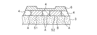
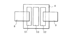
- FIG. 1 is a schematic plan view of an essential part showing a first example of the structure of the thin film transistor of the present embodiment
- FIG. 2 is a schematic sectional view of the relevant part as seen from the line II-II in FIG.
- a thin film transistor TFT: Thin Film Transistor, also referred to as a TFT substrate
- TFT substrate Thin Film Transistor
- a film 3 for example, TEOS for an organic film, SiO 2 film, SiO 2 / SiN film stack, SiN film, SiON film, etc. for an inorganic film
- TEOS for an organic film, SiO 2 film, SiO 2 / SiN film stack, SiN film, SiON film, etc. for an inorganic film
- a first amorphous silicon layer (also referred to as an a-Si film) 4 and a first amorphous silicon are formed on the surface of the gate insulating film 3 and above the gate electrode 2.
- a plurality of polysilicon layers 51 and 52 also referred to as p-Si films) separated by the layer 4 and having a required separation dimension (indicated by symbol X in FIG. 1).
- a microcrystal having a crystal grain size relatively smaller than that of a polycrystal or a single crystal having higher crystallinity is also formed.
- a second amorphous silicon layer 6 (a-Si film) is formed above the polysilicon layers 51 and 52 and the first amorphous silicon layer 4.
- the first amorphous silicon layer 4 and the second amorphous silicon layer 6 are collectively referred to simply as an amorphous silicon layer.
- the gate electrode 2, the second amorphous silicon layer 6 and the like are omitted for the sake of simplicity.
- n + silicon layer (n + Si film) 7 is formed at a required position on the surface of the second amorphous silicon layer 6.
- the n + silicon layer 7 is a contact layer with the source electrode 8 and the drain electrode 9 and is a semiconductor layer having a high impurity concentration such as phosphorus or arsenic.
- a source electrode 8 and a drain electrode 9 having a required pattern are formed on the surface of the n + silicon layer 7, the side surfaces of the second amorphous silicon layer 6 and the first amorphous silicon layer 4, and the surface of the gate insulating film 3. is there.
- both the source electrode 8 and one polysilicon layer 51 are projected onto the surface of the substrate 1, both the source electrode 8 and the polysilicon layer 51 are partially overlapped.
- both the drain electrode 9 and the other polysilicon layer 52 are projected onto the surface of the substrate 1, both the drain electrode 9 and the polysilicon layer 52 are partially overlapped.
- the channel region between the source electrode 8 and the drain electrode 9 has two polysilicon layers 51 and 52 formed separately, and the two polysilicon layers 51 and 52 have a required separation dimension X. And the first amorphous silicon layer 4 to be separated.
- the second amorphous silicon layer 6 is for preventing the source electrode 8 and the drain electrode 9 from directly contacting the channel region, and uses a characteristic with a small off-current. Since the channel region between the source electrode 8 and the drain electrode 9 has a structure in which the polysilicon layers 51 and 52 are separated from each other by the first amorphous silicon layer 4, compared with the case where the entire channel region is a polysilicon layer. , The off-current can be reduced.
- the channel region is constituted by the first amorphous silicon layer 4 and the polysilicon layers 51 and 52, and the first amorphous silicon layer 4 is separated so that the polysilicon layers 51 and 52 are separated from each other.
- the first amorphous silicon layer 4 between the polysilicon layers 51 and 52 is not subjected to laser annealing at all, and the crystallization rate can be defined as 0 when defined by the crystallization rate.
- the crystallization rate in the length direction of the channel region of the polysilicon layer is set for the purpose of reducing the off-current. It is also possible to adopt a method of changing. For example, a configuration is conceivable in which the crystallization rate in the channel region near the source and drain electrodes is increased and the crystallization rate in the vicinity of the center of the channel region is decreased. However, since laser annealing is performed on the entire channel region, it is very difficult to leave an amorphous silicon layer with a crystallization rate of 0. Further, since the crystallization rate is increased in order to improve the crystallization rate of the entire channel region, the crystallization rate near the center of the channel region cannot be reduced to zero.
- the entire channel region is formed of a polysilicon layer using a full surface irradiation type laser as shown in FIG. 15
- a method such as controlling the moving speed of the substrate is used to control the crystallization rate.
- the partial irradiation type laser as shown in FIG. 4 since the partial irradiation type laser as shown in FIG. 4 is used, the polysilicon layers 51 and 52 are used.
- the separation distance X can be freely controlled to a required value.
- the polysilicon layers 51 and 52 and the first amorphous silicon layer 4 between the polysilicon layers 51 and 52 correspond to a channel region.
- the first amorphous silicon layer 4, the second amorphous silicon layer 6, and the polysilicon layer 5 are collectively referred to as a semiconductor layer.
- the TFT composed of the gate electrode 2, the semiconductor layer, the source electrode 8, the drain electrode 9 and the like shown in FIG. 2 is a TFT for a driving circuit for driving a pixel. Since TFTs for driving circuits are required to operate at high speed, polysilicon layers 51 and 52 having high electron mobility are used in the channel region. Further, the polysilicon layers 51 and 52 are separated by the first amorphous silicon layer 4 in order to reduce the off-current.
- a passivation film 10 made of, for example, SiN is formed on the entire TFT substrate so as to cover the source electrode 8 and the drain electrode 9, and an organic film 11 is formed on the surface of the passivation film 10 to form a surface. Is flattened.
- a through hole is formed at a required position of the passivation film 10 and the organic film 11, and the pixel electrode 12 and the drain electrode 9 (and the source electrode 8) are electrically connected through the through hole.
- the pixel electrode 12 is formed of a transparent conductive film (for example, ITO or IZO).
- FIG. 3 is a manufacturing process diagram showing an example of a manufacturing method of the thin film transistor of the present embodiment.
- the gate electrode 2 is formed on the glass substrate 1 (S11), and the gate insulating film 3 is formed on the surface of the glass substrate 1 so as to cover the gate electrode 2 (S12).
- An a-Si film 4 as a first amorphous silicon layer is formed on the surface of the glass substrate 1 on which the gate insulating film 3 is formed (S13).
- a dehydrogenation annealing process is performed (S14), and laser pre-cleaning is performed (S15).
- the a-Si film 4 is crystallized by a partial irradiation type laser (S16).
- the crystallization process is an annealing process (also referred to as a laser annealing process).
- a required portion of the a-Si film 4 is irradiated with an energy beam through a multi-lens array, and the required portion is formed on a polysilicon layer (poly). -Si film) 51, 52.
- the required part is on the upper side of the gate electrode 2 and is a part of the channel region between the source and the drain.
- an energy beam is irradiated to a region corresponding to two polysilicon layers 51 and 52 separated and separated with the first a-Si film 4 in the center of the channel region interposed therebetween.
- the energy beam for example, an ultraviolet excimer laser having a large absorption of an amorphous silicon layer (a-Si film) or a solid laser having a green wavelength or less can be used.
- FIG. 4 is a schematic diagram showing an example of the configuration of a partial irradiation type laser.
- the glass substrate 1 on which the a-Si film 4 is formed is placed on a mounting table (not shown) and is translated in the direction of the arrow in FIG. 4 at a required speed. is there.
- a multi-lens array is arranged in which individual lenses are arranged at an appropriate distance along a direction intersecting the moving direction of the glass substrate 1.
- n + Si film (n + silicon layer) 7 is formed on the surface of the a-Si film 6 (S19).
- the n + Si film 7 is a contact layer with the source electrode 8 and the drain electrode 9 and is a semiconductor layer having a high impurity concentration such as phosphorus or arsenic.
- the required pattern can be appropriately determined according to the arrangement or structure of the source electrode 8, the drain electrode 9, and the semiconductor layer.
- the a-Si films 4 and 6 and the n + Si film 7 are etched (S21), and the source electrode 8 and the drain electrode 9 are formed on the n + Si film 7 after the etching (S21). S22).
- the manufacturing method of the present embodiment instead of irradiating the entire surface of the substrate with an energy beam (for example, a laser), the first amorphous silicon layer 4 in the center portion of the channel region of the first amorphous silicon layer 4 is applied.
- the energy beam is partially irradiated only to the regions that become the plurality of polysilicon layers 51 and 52 separated and separated with the first amorphous silicon layer 4 interposed therebetween, so that the channel region is formed only by the annealing process. can do.
- the exposure process, the development process, and the etching process are not required for the polysilicon layer crystallized over the entire substrate surface, and the manufacturing process can be shortened.
- FIG. 5 is a cross-sectional view of the main part near the channel region of the thin film transistor of the present embodiment.
- the boundary surfaces between the polysilicon layers 51 and 52 and the first amorphous silicon layer 4 (FIG. 5). Can be substantially perpendicular to the surface of the substrate. That is, since the line width on the gate electrode side of the polysilicon layers 51 and 52 does not become wider than the line width on the source electrode and drain electrode side, the separation dimension between the polysilicon layers 51 and 52 should be set with high accuracy. Can do.
- the first amorphous silicon layer 4 has the same thickness as the plurality of polysilicon layers 51 and 52.
- the plurality of polysilicon layers 51 and 52 are obtained by changing only the region corresponding to a part of the channel region to the polycrystalline state in the first amorphous silicon layer 4 formed on the upper side of the gate electrode 2. It can be seen that the exposure, development and etching processes are not performed to form the channel region.
- FIG. 6 is a schematic plan view of a main part showing a second example of the structure of the thin film transistor of the present embodiment
- FIG. 7 is a schematic cross-sectional view of the main part seen from the line VII-VII in FIG.
- the shapes of the polysilicon layers 51 and 52 in plan view are different from those in the first embodiment.
- the dimension in the width direction intersecting the length direction of the channel regions of the source electrode 8 and the drain electrode 9 is represented by W.
- the dimension in the width direction of the portion where the polysilicon layer 51 overlaps the source electrode 8 and the dimension in the width direction of the portion where the polysilicon layer 52 overlaps the drain electrode 9 are represented by d.
- the polysilicon layers 51 and 52 are formed so as to satisfy the relationship of W> d. Thereby, the off current between the source electrode 8 and the polysilicon layer 51 and the off current between the drain electrode 9 and the polysilicon layer 52 can be further reduced.
- the width dimension of the portion where the polysilicon layer 51 overlaps the source electrode 8 is constant, and the width dimension of the portion where the polysilicon layer 52 overlaps the drain electrode 9 is constant. is there.
- FIG. 8 is a schematic plan view of an essential part showing a third example of the structure of the thin film transistor of the present embodiment.
- the width direction dimension of the portion where the polysilicon layer 51 overlaps the source electrode 8 is made smaller toward the tip.
- the dimension in the width direction of the portion where the polysilicon layer 52 overlaps the drain electrode 9 is made smaller toward the tip.
- FIG. 9 is a schematic plan view of an essential part showing a fourth example of the structure of the thin film transistor of the present embodiment.
- the width direction dimensions of the polysilicon layers 51 and 52 are substantially the same as the width direction dimensions of the source electrode 8 and the drain electrode 9.
- the width dimension of the polysilicon layer 51 is made to decrease from the middle toward the source electrode 8.
- the width dimension of the polysilicon layer 52 is made to decrease from the middle toward the drain electrode 9.
- FIG. 10 is a schematic plan view of a main part showing a fifth example of the structure of the thin film transistor of the present embodiment.
- the channel region is composed of three polysilicon layers 51, 52, 53, and the first amorphous silicon layer 4 is interposed between the polysilicon layers 51, 52.
- the polysilicon layers 52 and 53 are separated and separated by the first amorphous silicon layer 4 while being separated and separated.
- the off-current can be reduced as compared with the case where the entire channel region is a polysilicon layer.
- the source electrode 8 and the polysilicon layer 51 are projected onto the surface of the substrate 1, both the source electrode 8 and the polysilicon layer 51 are partially overlapped.
- both the drain electrode 9 and the polysilicon layer 52 are projected onto the surface of the substrate 1, both the drain electrode 9 and the polysilicon layer 52 are partially overlapped.
- the total of the separation dimension between the polysilicon layers 51 and 53 and the separation dimension between the polysilicon layers 53 and 52 can be made substantially the same as the separation dimension X of the first embodiment.
- the width direction dimensions of the polysilicon layers 51 and 51 of the first embodiment are made smaller than the width direction dimensions of the source electrode 8 and the drain electrode 9. Also good.
- FIG. 11 is a schematic diagram illustrating an example of mobility and off-state current of the thin film transistor of this embodiment.
- the horizontal axis indicates the separation dimension X between the polysilicon layers 51 and 52
- the vertical axis indicates mobility and off current.
- the mobility of the thin film transistor has a characteristic of decreasing as the separation dimension X increases.
- the off-state current of the thin film transistor also has a characteristic of decreasing as the separation dimension X increases. Note that the straight lines indicating the mobility and the off-state current in FIG. 11 are schematically shown for simplicity, and may differ from actual characteristics.
- the separation dimension X between the polysilicon layers 51 and 52 in the channel region is in the range of 0.1 ⁇ m to 5 ⁇ m.
- the entire substrate on which the a-Si layer is formed is irradiated with laser to change the a-Si layer into a polycrystalline p-Si layer, and after crystallization, exposure, development and etching processes In the process of forming a p-Si layer using, it is very difficult to make the distance between adjacent polysilicon layers less than 5 ⁇ m.
- a method partial laser annealing in which laser light from a laser light source is incident on a multi-lens array, for example, as shown in FIG.
- the distance between adjacent polysilicon layers can be reduced to about 0.1 ⁇ m. That is, by using the partial laser annealing, the separation dimension of the polysilicon layer separated by the first amorphous silicon layer in the channel region can be in the range of 0.1 ⁇ m to 5 ⁇ m.
- the separation dimension X between the polysilicon layers 51 and 52 in the channel region can be further in the range of 1 ⁇ m to 2 ⁇ m.
- the separation dimension is larger than 2 ⁇ m, the ratio of the length of the amorphous silicon layer 4 to the length of the channel region increases, and the mobility of electrons in the channel region decreases.
- the separation dimension X is 2.5 ⁇ m or less and preferably 2 ⁇ m or less in consideration of errors. be able to.
- the separation dimension X when the separation dimension X is smaller than 1 ⁇ m, the ratio of the length of the amorphous silicon layer 4 to the length of the channel region is decreased, and the off-current exceeds an allowable value (for example, about 1 pA).
- an allowable value for example, about 1 pA.
- the separation dimension X should be 0.5 ⁇ m or more, and preferably 1 ⁇ m or more in consideration of errors. Can do.
- the off-current can be reduced without reducing the electron mobility in the channel region.
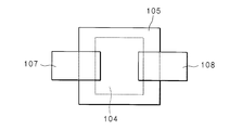
- FIG. 12 is a schematic cross-sectional view of the relevant part showing the structure of a conventional thin film transistor
- FIG. 13 is a schematic plan view of the relevant part showing the structure of the conventional thin film transistor.
- a gate electrode 102 is formed on the surface of a glass substrate 100, and a gate insulating film 103 is formed so as to cover the gate electrode 102.
- a polysilicon layer (poly-Si film) 104 is formed on the surface of the gate insulating film 103 and above the gate electrode 102.
- An amorphous silicon layer (a-Si film) 105 is formed so as to cover the polysilicon layer 104.
- An n + silicon layer (n + Si film) 106 is formed at a required position on the surface of the amorphous silicon layer 105.
- a source electrode 107 and a drain electrode 108 having a required pattern are formed on the surface of the n + silicon layer 106, the side surface of the amorphous silicon layer 105, and the surface of the gate insulating film 103. Further, as shown in FIG. 12, the entire channel region is formed of the polysilicon layer 104. For this reason, although the mobility of electrons is large, there is a problem that the off-current becomes large.
- the boundary surface between the polysilicon layer 104 and the amorphous silicon layer 105 is indicated by reference numeral C in FIG. Is not substantially perpendicular to a plane parallel to the surface of the substrate (indicated by reference numeral D), but is tapered.
- reference numeral D the boundary surface between the polysilicon layer 104 and the amorphous silicon layer 105
- the line width differs between the upper surface side and the lower surface side of the polysilicon layer 104, and the line width on the lower surface side becomes wider. Therefore, in the conventional thin film transistor, it is difficult to set the length and width of the polysilicon layer 104 to required values.
- FIG. 14 is a manufacturing process diagram showing a conventional method of manufacturing a thin film transistor. As shown in FIG. 14, a gate electrode 102 is formed on a glass substrate 101 (S101), and a gate insulating film 103 is formed on the surface of the glass substrate 101 so as to cover the gate electrode 102 (S102).
- An a-Si film is formed on the surface of the glass substrate 101 on which the gate insulating film 103 is formed (S103).
- a dehydrogenation annealing process is performed (S104), and laser pre-cleaning is performed (S105).
- the a-Si film is crystallized by the whole surface irradiation type laser (S106).
- FIG. 15 is a schematic diagram showing an example of the configuration of a conventional full-irradiation laser.
- the glass substrate 101 on which the a-Si film is formed is placed on a mounting table (not shown) and is translated in the direction of the arrow in FIG. 15 at a required speed.
- a mirror having a length substantially the same as the width direction of the glass substrate 101 (direction intersecting the direction of parallel movement) is disposed.
- the laser light is irradiated on the entire surface of the glass substrate 101.
- the a-Si film is entirely changed to a polysilicon layer (p-Si film).
- n + Si film (n + silicon layer) 106 is formed on the surface of the a-Si film 105 (S111).
- an exposure process and a development process are performed (S112), and the a-Si film 105 and the n + Si film 106 are etched (S113) to make the semiconductor layer have a required structure, and the source is formed on the n + Si film 106 after the etching.
- the electrode 107 and the drain electrode 108 are formed (S114).
- the amorphous silicon layer formed on the entire surface of the substrate is irradiated with an energy beam (for example, laser) over the entire surface of the substrate to be changed into a polysilicon layer, and then the polysilicon layer is irradiated.
- the entire surface of the substrate is not irradiated with an energy beam (for example, a laser).
- the energy beam is partially irradiated to only a required region of the channel region in the first amorphous silicon layer, the polysilicon layer in the channel region can be formed only by the annealing process. For this reason, the steps of exposure, development, and etching for forming the channel region (steps S107 and S108 shown in FIG. 14) are unnecessary, and the manufacturing process can be shortened.
- the thin film transistor of this embodiment can be used for a display panel. That is, the thin film transistor (TFT substrate) of this embodiment and the color filter substrate having the colors of R (red), G (green), and B (blue) are bonded to each other with a necessary gap, and the TFT substrate and the color are bonded. By injecting liquid crystal between the filter substrate, a TFT liquid crystal display panel (liquid crystal display) can be manufactured. Accordingly, a display panel with low off-state current can be provided.
Abstract
Description
2 ゲート電極
3 ゲート絶縁膜
4 第1のアモルファスシリコン層
51、52、53 ポリシリコン層
6 第2のアモルファスシリコン層
7 n+シリコン層
8 ソース電極
9 ドレイン電極 1 Glass substrate (substrate)
2
Claims (6)
- 薄膜トランジスタにおいて、
基板の表面に形成されたゲート電極と、
該ゲート電極の上側に形成された第1のアモルファスシリコン層と、
該第1のアモルファスシリコン層により分離され、所要の離隔寸法を有して前記ゲート電極の上側に形成された複数のポリシリコン層と、
該複数のポリシリコン層及び前記第1のアモルファスシリコン層の上側に形成された第2のアモルファスシリコン層及びn+シリコン層と、
該n+シリコン層上に形成されたソース電極及びドレイン電極と
を備えることを特徴とする薄膜トランジスタ。 In thin film transistors,
A gate electrode formed on the surface of the substrate;
A first amorphous silicon layer formed on the gate electrode;
A plurality of polysilicon layers separated by the first amorphous silicon layer and having a required separation dimension and formed on the gate electrode;
A second amorphous silicon layer and an n + silicon layer formed above the plurality of polysilicon layers and the first amorphous silicon layer;
A thin film transistor comprising: a source electrode and a drain electrode formed on the n + silicon layer. - 前記離隔寸法は、0.1μmから5μmの範囲内であることを特徴とする請求項1に記載の薄膜トランジスタ。 2. The thin film transistor according to claim 1, wherein the separation dimension is in a range of 0.1 μm to 5 μm.
- 前記離隔寸法は、さらに、1μmから2μmの範囲内であることを特徴とする請求項1又は請求項2に記載の薄膜トランジスタ。 3. The thin film transistor according to claim 1, wherein the separation dimension is further within a range of 1 μm to 2 μm.
- 前記第1のアモルファスシリコン層は、前記複数のポリシリコン層と同程度の厚みを有することを特徴とする請求項1から請求項3までのいずれか1項に記載の薄膜トランジスタ。 The thin film transistor according to any one of claims 1 to 3, wherein the first amorphous silicon layer has a thickness comparable to the plurality of polysilicon layers.
- 前記複数のポリシリコン層と第1のアモルファスシリコン層との境界面は、前記基板の表面に対して略垂直をなすことを特徴とする請求項1から請求項4までのいずれか1項に記載の薄膜トランジスタ。 5. The interface according to claim 1, wherein a boundary surface between the plurality of polysilicon layers and the first amorphous silicon layer is substantially perpendicular to a surface of the substrate. Thin film transistor.
- 請求項1から請求項5までのいずれか1項に記載の薄膜トランジスタを備えることを特徴とする表示パネル。 A display panel comprising the thin film transistor according to any one of claims 1 to 5.
Priority Applications (4)
| Application Number | Priority Date | Filing Date | Title |
|---|---|---|---|
| CN201580078351.7A CN107408578B (en) | 2015-03-30 | 2015-03-30 | Thin film transistor and display panel |
| US15/561,686 US10008606B2 (en) | 2015-03-30 | 2015-03-30 | Thin film transistor and display panel |
| PCT/JP2015/059860 WO2016157351A1 (en) | 2015-03-30 | 2015-03-30 | Thin film transistor and display panel |
| JP2017508877A JPWO2016157351A1 (en) | 2015-03-30 | 2015-03-30 | Thin film transistor and display panel |
Applications Claiming Priority (1)
| Application Number | Priority Date | Filing Date | Title |
|---|---|---|---|
| PCT/JP2015/059860 WO2016157351A1 (en) | 2015-03-30 | 2015-03-30 | Thin film transistor and display panel |
Publications (1)
| Publication Number | Publication Date |
|---|---|
| WO2016157351A1 true WO2016157351A1 (en) | 2016-10-06 |
Family
ID=57004875
Family Applications (1)
| Application Number | Title | Priority Date | Filing Date |
|---|---|---|---|
| PCT/JP2015/059860 WO2016157351A1 (en) | 2015-03-30 | 2015-03-30 | Thin film transistor and display panel |
Country Status (4)
| Country | Link |
|---|---|
| US (1) | US10008606B2 (en) |
| JP (1) | JPWO2016157351A1 (en) |
| CN (1) | CN107408578B (en) |
| WO (1) | WO2016157351A1 (en) |
Cited By (7)
| Publication number | Priority date | Publication date | Assignee | Title |
|---|---|---|---|---|
| CN106784016A (en) * | 2017-01-25 | 2017-05-31 | 京东方科技集团股份有限公司 | A kind of thin film transistor (TFT), preparation method, display base plate and display device |
| US10559600B2 (en) | 2018-06-28 | 2020-02-11 | Sakai Display Products Corporation | Thin film transistor, display device and method for producing thin film transistor |
| CN110870078A (en) * | 2017-07-12 | 2020-03-06 | 堺显示器制品株式会社 | Semiconductor device and method for manufacturing the same |
| US10770483B2 (en) | 2018-06-28 | 2020-09-08 | Sakai Display Products Corporation | Thin film transistor, display device and method for manufacturing thin film transistor |
| US11121262B2 (en) | 2017-07-12 | 2021-09-14 | Sakai Display Products Corporation | Semiconductor device including thin film transistor and method for manufacturing the same |
| US11133333B2 (en) | 2018-06-28 | 2021-09-28 | Sakai Display Products Corporation | Producing method for thin film transistor with different crystallinities |
| US11495689B2 (en) | 2018-08-08 | 2022-11-08 | Sakai Display Products Corporation | Thin-film transistor and method for producing same |
Families Citing this family (6)
| Publication number | Priority date | Publication date | Assignee | Title |
|---|---|---|---|---|
| KR102365963B1 (en) * | 2015-06-23 | 2022-02-23 | 삼성디스플레이 주식회사 | Thin film transistor, method of manufacturing the same and liquid crystal display apparatus having the same |
| WO2017187486A1 (en) * | 2016-04-25 | 2017-11-02 | 堺ディスプレイプロダクト株式会社 | Thin film transistor, display device, and thin film transistor manufacturing method |
| CN107634011A (en) * | 2017-09-20 | 2018-01-26 | 武汉华星光电半导体显示技术有限公司 | A kind of array base palte and its manufacture method |
| JP7022592B2 (en) * | 2018-01-11 | 2022-02-18 | 株式会社ジャパンディスプレイ | Display device |
| CN110137261A (en) * | 2018-10-29 | 2019-08-16 | 京东方科技集团股份有限公司 | Thin film transistor (TFT) and preparation method thereof, array substrate and display device |
| CN113611752B (en) * | 2021-07-19 | 2024-01-16 | Tcl华星光电技术有限公司 | Manufacturing method of low-temperature polysilicon TFT (thin film transistor) and low-temperature polysilicon TFT |
Citations (5)
| Publication number | Priority date | Publication date | Assignee | Title |
|---|---|---|---|---|
| JPH08195495A (en) * | 1994-05-31 | 1996-07-30 | Sanyo Electric Co Ltd | Semiconductor device, manufacture of semiconductor device, film transistor, manufacture of film transistor, and display |
| JP2000114529A (en) * | 1998-09-30 | 2000-04-21 | Sanyo Electric Co Ltd | Semiconductor device |
| JP2005197719A (en) * | 2003-12-30 | 2005-07-21 | Samsung Electronics Co Ltd | Semiconductor device having adjusted mobility and thin film transistor to which the same is applied |
| JP2009289874A (en) * | 2008-05-28 | 2009-12-10 | Sony Corp | Thin-film transistor and display unit |
| WO2011010611A1 (en) * | 2009-07-24 | 2011-01-27 | 株式会社ブイ・テクノロジー | Thin-film transistor, manufacturing method therefor, and liquid-crystal display device |
Family Cites Families (10)
| Publication number | Priority date | Publication date | Assignee | Title |
|---|---|---|---|---|
| JPH0563196A (en) * | 1991-09-04 | 1993-03-12 | Hitachi Ltd | Thin film semiconductor device, manufacture thereof and liquid crystal display device |
| JP3352191B2 (en) * | 1993-12-08 | 2002-12-03 | キヤノン株式会社 | Method for manufacturing thin film transistor |
| TWI266386B (en) * | 2001-10-03 | 2006-11-11 | Hannstar Display Corp | Dual vertical cannel thin film transistor for SRAM and manufacturing method thereof |
| US7007481B2 (en) * | 2003-09-10 | 2006-03-07 | General Electric Company | Thick coated combustor liner |
| KR100646937B1 (en) * | 2005-08-22 | 2006-11-23 | 삼성에스디아이 주식회사 | Poly silicon thin film transistor and method for fabricating the same |
| JP5226259B2 (en) | 2007-08-21 | 2013-07-03 | 株式会社ジャパンディスプレイイースト | Liquid crystal display |
| KR100974610B1 (en) * | 2007-12-28 | 2010-08-06 | 주식회사 비아트론 | The Method for Manufacturing Thin Film Transistor |
| JP5688223B2 (en) * | 2010-02-03 | 2015-03-25 | 三菱電機株式会社 | THIN FILM TRANSISTOR, SEMICONDUCTOR DEVICE, AND METHOD FOR MANUFACTURING THIN FILM TRANSISTOR |
| JP5615605B2 (en) * | 2010-07-05 | 2014-10-29 | 三菱電機株式会社 | FFS mode liquid crystal device |
| CN103594521B (en) * | 2012-08-17 | 2017-03-01 | 瀚宇彩晶股份有限公司 | Semiconductor element |
-
2015
- 2015-03-30 WO PCT/JP2015/059860 patent/WO2016157351A1/en active Application Filing
- 2015-03-30 US US15/561,686 patent/US10008606B2/en not_active Expired - Fee Related
- 2015-03-30 CN CN201580078351.7A patent/CN107408578B/en not_active Expired - Fee Related
- 2015-03-30 JP JP2017508877A patent/JPWO2016157351A1/en active Pending
Patent Citations (5)
| Publication number | Priority date | Publication date | Assignee | Title |
|---|---|---|---|---|
| JPH08195495A (en) * | 1994-05-31 | 1996-07-30 | Sanyo Electric Co Ltd | Semiconductor device, manufacture of semiconductor device, film transistor, manufacture of film transistor, and display |
| JP2000114529A (en) * | 1998-09-30 | 2000-04-21 | Sanyo Electric Co Ltd | Semiconductor device |
| JP2005197719A (en) * | 2003-12-30 | 2005-07-21 | Samsung Electronics Co Ltd | Semiconductor device having adjusted mobility and thin film transistor to which the same is applied |
| JP2009289874A (en) * | 2008-05-28 | 2009-12-10 | Sony Corp | Thin-film transistor and display unit |
| WO2011010611A1 (en) * | 2009-07-24 | 2011-01-27 | 株式会社ブイ・テクノロジー | Thin-film transistor, manufacturing method therefor, and liquid-crystal display device |
Cited By (8)
| Publication number | Priority date | Publication date | Assignee | Title |
|---|---|---|---|---|
| CN106784016A (en) * | 2017-01-25 | 2017-05-31 | 京东方科技集团股份有限公司 | A kind of thin film transistor (TFT), preparation method, display base plate and display device |
| CN110870078A (en) * | 2017-07-12 | 2020-03-06 | 堺显示器制品株式会社 | Semiconductor device and method for manufacturing the same |
| US11081507B2 (en) | 2017-07-12 | 2021-08-03 | Sakai Display Products Corporation | Semiconductor device and method for manufacturing same |
| US11121262B2 (en) | 2017-07-12 | 2021-09-14 | Sakai Display Products Corporation | Semiconductor device including thin film transistor and method for manufacturing the same |
| US10559600B2 (en) | 2018-06-28 | 2020-02-11 | Sakai Display Products Corporation | Thin film transistor, display device and method for producing thin film transistor |
| US10770483B2 (en) | 2018-06-28 | 2020-09-08 | Sakai Display Products Corporation | Thin film transistor, display device and method for manufacturing thin film transistor |
| US11133333B2 (en) | 2018-06-28 | 2021-09-28 | Sakai Display Products Corporation | Producing method for thin film transistor with different crystallinities |
| US11495689B2 (en) | 2018-08-08 | 2022-11-08 | Sakai Display Products Corporation | Thin-film transistor and method for producing same |
Also Published As
| Publication number | Publication date |
|---|---|
| JPWO2016157351A1 (en) | 2018-01-18 |
| US20180097120A1 (en) | 2018-04-05 |
| CN107408578B (en) | 2020-08-11 |
| CN107408578A (en) | 2017-11-28 |
| US10008606B2 (en) | 2018-06-26 |
Similar Documents
| Publication | Publication Date | Title |
|---|---|---|
| WO2016157351A1 (en) | Thin film transistor and display panel | |
| US10438973B2 (en) | Display device and method for manufacturing same | |
| JP6503458B2 (en) | METHOD FOR MANUFACTURING THIN FILM TRANSISTOR AND DISPLAY PANEL | |
| JP6334057B2 (en) | Thin film transistor and display panel | |
| WO2016072024A1 (en) | Method for manufacturing thin-film transistor, thin-film transistor, and display panel | |
| US8148726B2 (en) | Display device and manufacturing method thereof | |
| WO2016098651A1 (en) | Semiconductor device and method for manufacturing same, and display device provided with semiconductor device | |
| US10310347B2 (en) | Display apparatus and method of manufacturing display apparatus | |
| US10263121B2 (en) | Thin film transistor and method of manufacturing thin film transistor | |
| TW201022814A (en) | Display device | |
| KR101338106B1 (en) | Liquid crystal display and method for fabricating the same | |
| US9041001B2 (en) | Thin film transistor array panel and manufacturing method thereof | |
| JP2010039394A (en) | Display, and manufacturing method for display | |
| US11081507B2 (en) | Semiconductor device and method for manufacturing same | |
| US11121262B2 (en) | Semiconductor device including thin film transistor and method for manufacturing the same | |
| WO2017168594A1 (en) | Thin film transistor, display panel, and method for manufacturing thin film transistor | |
| JP2009224396A (en) | Thin film transistor substrate and method of manufacturing the same, and display device | |
| JP2005345972A (en) | Method for manufacturing active matrix liquid crystal display | |
| JP2006317638A (en) | Method for manufacturing liquid crystal display apparatus | |
| JP2009059779A (en) | Thin film transistor, its manufacturing method, and display device |
Legal Events
| Date | Code | Title | Description |
|---|---|---|---|
| 121 | Ep: the epo has been informed by wipo that ep was designated in this application |
Ref document number: 15887504 Country of ref document: EP Kind code of ref document: A1 |
|
| ENP | Entry into the national phase |
Ref document number: 2017508877 Country of ref document: JP Kind code of ref document: A |
|
| WWE | Wipo information: entry into national phase |
Ref document number: 15561686 Country of ref document: US |
|
| NENP | Non-entry into the national phase |
Ref country code: DE |
|
| 122 | Ep: pct application non-entry in european phase |
Ref document number: 15887504 Country of ref document: EP Kind code of ref document: A1 |