WO2016148435A1 - 금속 메쉬 구조를 갖는 투명 전극 제조 방법 및 이를 이용하여 제조된 투명 전극 - Google Patents
금속 메쉬 구조를 갖는 투명 전극 제조 방법 및 이를 이용하여 제조된 투명 전극 Download PDFInfo
- Publication number
- WO2016148435A1 WO2016148435A1 PCT/KR2016/002362 KR2016002362W WO2016148435A1 WO 2016148435 A1 WO2016148435 A1 WO 2016148435A1 KR 2016002362 W KR2016002362 W KR 2016002362W WO 2016148435 A1 WO2016148435 A1 WO 2016148435A1
- Authority
- WO
- WIPO (PCT)
- Prior art keywords
- metal
- crystals
- transparent electrode
- substrate
- metal mesh
- Prior art date
- Legal status (The legal status is an assumption and is not a legal conclusion. Google has not performed a legal analysis and makes no representation as to the accuracy of the status listed.)
- Ceased
Links
Images


Classifications
-
- H—ELECTRICITY
- H01—ELECTRIC ELEMENTS
- H01B—CABLES; CONDUCTORS; INSULATORS; SELECTION OF MATERIALS FOR THEIR CONDUCTIVE, INSULATING OR DIELECTRIC PROPERTIES
- H01B1/00—Conductors or conductive bodies characterised by the conductive materials; Selection of materials as conductors
- H01B1/02—Conductors or conductive bodies characterised by the conductive materials; Selection of materials as conductors mainly consisting of metals or alloys
-
- H—ELECTRICITY
- H01—ELECTRIC ELEMENTS
- H01B—CABLES; CONDUCTORS; INSULATORS; SELECTION OF MATERIALS FOR THEIR CONDUCTIVE, INSULATING OR DIELECTRIC PROPERTIES
- H01B1/00—Conductors or conductive bodies characterised by the conductive materials; Selection of materials as conductors
- H01B1/06—Conductors or conductive bodies characterised by the conductive materials; Selection of materials as conductors mainly consisting of other non-metallic substances
- H01B1/08—Conductors or conductive bodies characterised by the conductive materials; Selection of materials as conductors mainly consisting of other non-metallic substances oxides
-
- H—ELECTRICITY
- H01—ELECTRIC ELEMENTS
- H01B—CABLES; CONDUCTORS; INSULATORS; SELECTION OF MATERIALS FOR THEIR CONDUCTIVE, INSULATING OR DIELECTRIC PROPERTIES
- H01B13/00—Apparatus or processes specially adapted for manufacturing conductors or cables
Definitions
- the present invention relates to a transparent electrode, and more particularly to a transparent electrode manufacturing method having a metal mesh structure and a transparent electrode manufactured using the same.
- Metal mesh structure refers to the formation of a network (network) shape using a metal.
- Metal mesh films applied to display devices are pointed out by visibility problems and moire (Moire) phenomenon.
- the visibility problem is a phenomenon in which a metal pattern is visible in a product implementation. This problem can be solved by blackening a black material on the pattern or minimizing the line width (thickness) of the pattern to less than 1.8m. In other words, producing fine particles is a key technology.
- the moiré phenomenon is a phenomenon in which the mesh pattern overlaps two sheets, and the grid pattern of the display is added to it, and it looks like a wave, which is a problem of pattern design.
- This is the key technology for the design of the pattern that transmits the electrical signal well, and the moire phenomenon is the most important issue because the moire phenomenon does not occur when the ultra fine line width of less than 1m. Therefore, fabrication of metal mesh with nano sized line width is essential.
- a method of dispersing nanostructures carbon nanotubes, silver nanowires, etc.
- a method of dispersing nanostructures on a solution and then applying them onto a substrate, forming a metal mesh through a photolithography process, roll printing, gravure printing, offset printing
- a method of forming a metal mesh using a printing method such as the above.
- the method of applying the nanostructure on the substrate has the advantage that it is possible to form a nano-scale metal mesh structure, but the particles are not organically connected to each other there is a limit to lower the resistance value, or nanoparticles There is a problem in that the transmittance deviation or Haze phenomenon of the formed metal mesh occurs due to the aggregation of these.
- the method of forming the metal mesh through photolithography has a problem that not only the process is complicated, but also the process cost and time consuming.
- the implementation of metal mesh with nano size line width through photolithography process has various technical difficulties.
- the method of forming a metal mesh using a conventional printing method has a problem that the mesh line width can not be reduced, and in the case of the electrostatic hydrodynamic method, the mesh line width can be reduced, but since the electric charge is partially accumulated on the insulator substrate, Not only does distortion of the mesh pattern occur, but a high driving voltage is required to reduce the line width of the metal mesh structure.
- the problem of the method of minimizing the line width and the problem of current spreading due to the network shape of the metal deteriorate.
- the network shape does not cover the entire surface in the form of a net. In other words, a gap in the plane unit is generated between the metal wire and the metal wire, so that current dispersion is not easy.
- indium tin oxide (ITO), indium zinc oxide (IZO), al-doped zinc oxide (AZO), ga-doped zinc oxide (GZO), and graphene layers are formed on and under the metal mesh pattern layer.
- the problem to be solved by the present invention is to provide a transparent electrode having a metal mesh structure that can solve the current dispersion problem while having a nano-sized line width in a simple process and a method of manufacturing the same.
- the transparent electrode manufacturing method having a metal mesh structure according to a preferred embodiment of the present invention for solving the above problems, (a) by depositing a first metal on a substrate, a plurality of first metal separated from each other on the substrate Forming crystals; (b) depositing a second metal on the substrate to form a second metal mesh that fills between the first metal crystals; And (c) performing heat treatment on the substrate to diffuse and oxidize the first metal and the second metal to each other to convert the first metal crystal into a transparent crystal including the first metal and the second metal. And forming a metal mesh to fill the gaps between the transparent crystals with the second metal.
- the transparent electrode manufacturing method having the metal mesh structure includes (d) the transparent The method may further include removing an oxide of the second metal remaining on the crystal.
- step (d) may remove together the oxidized surface of the metal mesh.
- heat treatment may be performed for 30 seconds to 2 minutes in an oxygen (O 2 ) of 300 ° C. to 700 ° C. or an atmospheric atmosphere.
- the second metal may be integrally deposited on the substrate between the first metal crystals and on the first metal crystals to a thickness greater than the thickness of the first metal crystals. Can be.
- step (c), (c1) the upper surface of the second metal, such that the thickness of the first metal crystals and the thickness of the second metal formed on the first metal crystals is a predefined ratio.
- step (c) may further include (c4) removing the surface of the metal mesh oxidized in the step (c3).
- the upper surface of the second metal may be flattened by performing dry etching or chemical mechanical planning (CMP).
- the step (c2) is carried out in a nitrogen and argon atmosphere, the heat treatment for about 15 to 30 minutes at a temperature of 300 °C to 500 °C, the step (c3) is 300 °C ⁇ 700 °C oxygen (O 2 ) Alternatively, the heat treatment may be performed for 30 seconds to 2 minutes in an air atmosphere.
- first metal and the second metal used in the transparent electrode manufacturing method having the metal mesh structure may be selected from metals whose oxides are transparent and conductive.
- the transparent electrode manufactured by the method of manufacturing a transparent electrode having a metal mesh structure according to the preferred embodiment of the present invention described above is formed on the substrate to be spaced apart from each other a plurality of, the oxide of the first metal and the second metal Mixed transparent crystals; And a metal mesh formed of the second metal on the substrate to fill between the transparent crystals.
- a method for manufacturing a transparent electrode having a metal mesh structure includes depositing a first metal on a substrate to form a plurality of first metal crystals separated from each other on a substrate, After the metal mesh is filled with the second metals to be constituted, heat treatment is performed to form a metal mesh formed of the second metal having a nano-sized line width, and the first metal and the second metal having high conductivity while providing a space between the metal meshes are transparent. It is filled with transparent crystals which are oxides of.
- the transparent electrode according to the preferred embodiment of the present invention can not only form a metal mesh having a nano-sized line width on the substrate without applying a complicated process such as a photographic vision process, but also the entire upper surface of the substrate with the metal mesh.
- a transparent crystal having high conductivity and transmittance it is possible to easily diffuse the current through the entire substrate while eliminating the variation in transmittance or Haze of the metal mesh, which is a problem of the existing metal mesh.
- FIG. 1 is a view for explaining a transparent electrode manufacturing method having a metal mesh structure according to a first embodiment of the present invention.
- FIG. 2 is a view for explaining a transparent electrode manufacturing method having a metal mesh structure according to a second embodiment of the present invention.
- FIG 3 illustrates a transparent electrode manufactured according to preferred embodiments of the present invention.
- FIG. 1 is a view for explaining a transparent electrode manufacturing method having a metal mesh structure according to a first embodiment of the present invention.
- a substrate 110 for forming a transparent electrode is prepared (see FIG. 1A).
- the substrate 110 of the present invention may be applied to any type of substrate to which the transparent electrode is applied.
- the substrate 110 on which the transparent electrode is to be formed is a semiconductor.
- An n-GaN, an active layer, and a p-GaN layer may be sequentially formed on the substrate, and when the transparent electrode of the present invention is applied to an organic light emitting device, the substrate 110 may have a structure in which an organic material is formed.
- the substrate 110 of the present invention may be a structure in which all structures to which the transparent electrode is applied are formed in advance.
- the first metal is deposited to form the first metal crystals 120 on the substrate 110 (see FIG. 1B).
- the crystal 120 is formed while the first metal is agglomerated, and as the deposition proceeds, the thickness and width of the crystal 120 gradually increase.
- the first metal crystals 120 should be formed to a thickness such that crystals formed of the first metal are not connected to each other to form a film.
- the width of the crystals 120 formed of the first metal in the deposition process should be formed in consideration of the distance between the first metal crystals to be subsequently filled and deposited with the second metal. That is, in the heat treatment process to be described later, the interval between the first metal crystals 120 may be set to be wider or narrower than the width of the first metal crystals 120 according to the degree of diffusion between the first metal and the second metal. have.
- indium (In) is applied as the first metal, but other metals may be applied.
- a second metal which will constitute the metal mesh is deposited on the substrate 110 and filled with the second metal to fill the space between the first metal crystals 120 with the second metal.
- the mesh 130 is formed (see FIG. 1C).
- the second metal 140 is also deposited on the first metal crystals 120.
- the second metal is selected such that the mixed oxide of the first metal and the second metal is a transparent and highly conductive material.
- the first metal is indium (In)
- Sn or Zn is selected as the second metal
- the oxide of the mixed material is indium tin oxide (ITO) or IZO.
- the second metal is selected to be (Indium-Zinc Oxide) to become a material having high conductivity and permeability.
- Zn may be selected as the second metal so that the oxide of the mixed material is AZO.
- the area of the mixed region of the first metal and the second metal is larger than the area occupied by the first metal crystal 120, and the line width of the metal mesh 130 composed of the second metal is smaller.
- the first metal crystal 120 formed of indium (In) and the metal mesh 130 formed of tin (Sn) have indium (In) and tin (Sn) at a contact surface thereof.
- the interdiffusion causes the region where indium (In) and tin (Sn) are mixed to be larger than the region of the first metal crystal 120, and the line width of the metal mesh 130 formed of tin (Sn) is relatively reduced. do.
- the crystal mixed with indium and tin is a transparent crystal 160 mixed with indium oxide (In 2 O 3 ) and tin oxide (SnO 2 ), that is, ITO (Indium- Tin Oxide), and tin oxide 130-2a is similarly formed on the surface of the metal mesh 130-2.
- the oxide (SnO 2 ) 130-2a of the second metal formed on the ITO which is the transparent crystal 160 and on the metal mesh 130-2b is transparent and conductive. Therefore, even if it is not removed, the implementation of the transparent electrode of the present invention does not interfere.
- the second metal oxide 140-2 and the metal mesh formed on the ITO which is the transparent crystal 160 are formed.
- the second metal oxide 130-2a formed on the surface may be removed.
- FIG. 2 is a view for explaining a transparent electrode manufacturing method having a metal mesh structure according to a second embodiment of the present invention.
- the first metal crystals 220 are formed on a substrate 210 in the same manner as shown in FIGS. 1A and 1B. To form (see FIG. 2 (a)).
- a second metal 230 constituting the metal mesh is deposited on the substrate 210 to form the first metal crystals 220 as the second metal 230.
- the metal mesh is formed from the second metal by filling the gaps (see FIG. 2B).
- the second metal is thickly deposited so that the metal mesh filled between the first metal crystals 220 and the second metal formed on the first metal crystals are integrally connected in the deposition process.
- the first metal is Indium (In) and the second metal is Tin (Sn) is exemplarily described.
- the top surface of the second metal is removed to be flat such that the thickness of the first metal crystals 220 and the thickness of the second metal 230 formed thereon are a predetermined ratio (see FIG. c)).
- the top surface of the second metal 230 is removed such that the ratio of the thickness of the first metal crystal 220 to the thickness of the second metal 230 is about 9: 1.
- the thickness ratio may vary depending on the process conditions or the characteristics of the first metal and the second metal.
- all applicable processes such as a dry etching method and a chemical mechanical planarization (CMP) process may be used as a method of removing the second metal.
- the substrate 210 is heat-treated as shown in FIG. 2 (d) to diffuse the first metal crystal and the second metal to each other, and as shown in FIG. 2 (e).
- the metal mesh 230 filling the mixed metal crystals 240 and the mixed metal crystals 240 is formed.
- the heat treatment process shown in (d) of FIG. 2 is merely for diffusion between the first metal and the second metal, and is performed at a temperature of 300 ° C. to 500 ° C. in a nitrogen and argon atmosphere for about 15 to 30 minutes. Is performed.
- the mesh of the mixed metal crystal 240 including the first metal and the second metal and the second metal filling the mixed metal crystals is filled. Line 230 is formed.
- the metal mesh 230 of the second metal filling between the mixed metal crystals 240 and the mixed metal crystals 240 is formed, 30 seconds to 2 minutes in oxygen (O 2 ) or an atmosphere of 300 ° C. to 700 ° C.
- the heat treatment is performed to change the mixed metal crystals 240 into the transparent crystals 260 (see FIG. 2F).
- the indium and the tin contained in the mixed metal crystal 240 are combined with oxygen, respectively, to be changed to indium oxide (In 2 O 3 ) and tin oxide (SnO 2 ), so that the transparent crystal 260 which is ITO is obtained. Is formed.
- the transparent crystal 260 may be formed of indium tin oxide (ITO), indium zinc oxide (IZO), al-doped zinc oxide (AZO), or Ga-doped zinc oxide (GZO). It can be formed as.
- ITO indium tin oxide
- IZO indium zinc oxide
- AZO al-doped zinc oxide
- GZO Ga-doped zinc oxide
- the surface of the metal mesh 230 formed of the second metal is also oxidized.
- tin oxide (SnO 2 ) 230-2a is formed on the surface of the metal mesh during the heat treatment.
- the transparent electrode of the present invention does not need to be removed.
- the surface of the metal mesh 230-2 is formed by etching the surface of the ITO surface and the metal mesh 230-2, which are transparent crystals 260, or performing a chemical mechanical planarization (CMP) process.
- CMP chemical mechanical planarization
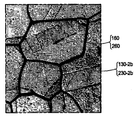
- FIG 3 illustrates a transparent electrode manufactured according to preferred embodiments of the present invention.
- metal meshes 130-2b and 230-2b having a line width of several nanometers are formed, and a space between the metal meshes 130-2b and 230-2b is formed.
- Transparent crystals 160 and 260 which are transparent conductive materials, are formed on the surface of the transparent crystals, so that the current can be diffused through the transparent crystals as well as the metal mesh without significantly inhibiting light transmittance.
Landscapes
- Engineering & Computer Science (AREA)
- Manufacturing & Machinery (AREA)
- Electroluminescent Light Sources (AREA)
- Manufacturing Of Electric Cables (AREA)
- Laminated Bodies (AREA)
Abstract
본 발명은 금속 메쉬 구조를 갖는 투명 전극 제조 방법 및 이를 이용하여 제조된 투명 전극을 공개한다. 본 발명의 바람직한 실시예에 따른, 금속 메쉬 구조를 갖는 투명 전극 제조 방법은, 기판위에 제 1 금속을 증착하여 기판 위에 서로 분리된 복수의 제 1 금속 결정체들을 형성하고, 제 1 금속 결정체들 사이를 금속 메쉬를 구성할 제 2 금속들로 채운 후 열처리를 수행하여, 선폭이 나노 사이즈인 제 2 금속으로 형성된 금속 메쉬를 형성하고, 금속 메쉬 사이 공간을 투명하면서도 전도도가 높은 제 1 금속과 제 2 금속의 산화물인 투명 결정체로 채운다. 따라서, 본 발명의 바람직한 실시예에 따른 투명 전극은 사진 시각 공정과 같은 복잡한 공정을 적용하지 않고서도 기판위에 선폭이 나노 사이즈인 금속 메쉬를 형성할 수 있을뿐만 아니라, 기판 상부면 전체를 금속 메쉬와 높은 전도도 및 투과도를 갖는 투명 결정체로 형성함으로써 용이하게 전류를 기판 전체로 확산시키면서도 기존의 금속 메쉬의 문제점인 금속 메쉬의 투과도 편차 또는 Haze 현상을 제거하는 효과가 있다.
Description
본 발명은 투명 전극에 관한 것으로서, 보다 구체적으로는 금속 메쉬 구조를 갖는 투명 전극 제조 방법 및 이를 이용하여 제조된 투명 전극에 관한 것이다.
금속 메쉬 구조(Metal Mesh Structure)란 금속을 이용하여 망(network) 형상을 형성시킨 것을 의미한다. 디스플레이 장치에 적용되는 Metal Mesh 필름은 시인성 문제와 모아레(Moire) 현상이 단점으로 지적된다. 시인성 문제란 제품 구현시 메탈 패턴이 눈에 보이는 현상인데, 이러한 문제는 패턴에 검정 물질을 입히는 흑화 방식 또는 패턴의 선폭(두께)을 1.8m 미만으로 미세화시킴으로써 해결할 수 있다. 즉, 미세한 입자를 만들어 내는 것이 핵심 기술력이다.
모아레 현상이란 메쉬 패턴이 2장 겹쳐지며 여기에 디스플레이의 격자무늬가 더해져서 물결처럼 보이는 현상으로 패턴 설계의 문제라고 볼 수 있다. 이는 전기적 신호를 잘 전달하는 패턴의 설계가 핵심 기술이며, 모아레 현상도 1m 이하의 초미세 선폭을 구현할 경우 발생하지 않기 때문에 미세 선폭 구현은 가장 중요한 사안이다. 따라서 nano 사이즈의 선폭을 갖는 Metal Mesh 제작이 필수적이다.
이러한 금속 메쉬 구조를 형성시키기 위하여, 다양한 방법들이 이용되고 있다. 예를 들면, 나노 구조체(탄소나노튜브, 은 나노선 등)를 용액 상에 분산시킨 후에 기판 상에 도포하는 방법, 사진 식각 공정을 통해 금속 메쉬를 형성하는 방법, 롤 인쇄, 그라비아 인쇄, 옵셋 인쇄 등의 인쇄법을 이용하여 금속 메쉬를 형성하는 방법 등이 있다.
그런데, 나노 구조체를 기판 상에 도포하는 방법의 경우에는 나노 스케일의 금속 메쉬 구조를 형성 가능하다는 장점이 있으나, 입자들이 서로 유기적으로 연결된 상태가 아니어서 저항값을 낮추는 데에 한계가 있거나, 나노 입자들의 뭉침(aggregation) 현상 등으로 인해 형성된 금속 메쉬의 투과도 편차 또는 Haze 현상이 발생한다는 문제점이 있다.
한편, 사진식각공정(photolithography)을 통해 금속 메쉬를 형성하는 방법은 공정이 복잡할 뿐만 아니라, 공정비용 및 시간이 많이 소요된다는 문제점이 있었다. 특히 사진식각공정을 통한 nano 사이즈의 선폭을 가지는 Metal Mesh의 구현은 여러 기술적 어려움을 가지고 있다.
또한, 종래 인쇄법을 이용하여 금속 메쉬를 형성하는 방법은 메쉬 선폭을 줄일 수 없다는 문제가 있으며, 정전기 수력학 방식의 경우에는 메쉬 선폭을 줄일 수 있으나 절연체 기판 상에 부분적으로 전하가 누적되게 되므로 금속 메쉬 패턴의 왜곡이 일어나는 현상이 발생할 뿐만 아니라, 금속 메쉬 구조의 선폭을 줄이기 위해서는 높은 구동전압이 요구되는 문제점이 있다.
또한, Metal Mesh를 적용하는 경우, 선폭을 초미세화시키는 방법의 문제와 더불어 금속의 망(network) 형상에 의한 전류 분산(spreading)이 나빠지는 문제도 해결되어야 한다. 망(network) 형상은 그물 형태로 표면 전체를 덮지 못한다. 즉, 금속선과 금속선 사이에 면 단위의 공백이 생겨서 전류 분산이 용이치 못하다. 이러한 문제를 해결하기 위해, Metal Mesh 패턴층 위와 아래에 ITO(Indium Tin Oxide), IZO(Indium Zinc Oxide), AZO(Al-doped Zinc Oxide), GZO(Ga-doped Zinc Oxide), Graphene layer 등의 박막을 함께 구성하는 기술이 적용되고 있지만, 이중층에 의한 투과도 감소 문제, 공정의 복잡화, 접착력(adhesion) 등의 문제점이 발생하고 있는 실정이다. 따라서, 더 간단하게 nano 크기의 선폭을 갖는 Metal Mesh를 형성 할 수 있는 방법과 전류 분산을 해결할 수 있는 방법의 개발이 요구된다.
본 발명이 해결하고자 하는 과제는, 간단한 공정으로 nano 크기의 선폭을 갖으면서도 전류 분산 문제를 해결할 수 있는 금속 메쉬 구조를 갖는 투명 전극 및 그 제조 방법을 제공하는 것이다.
상술한 과제를 해결하기 위한 본 발명의 바람직한 실시예에 따른 금속 메쉬 구조를 갖는 투명 전극 제조 방법은, (a) 기판 위에 제 1 금속을 증착하여, 상기 기판 위에 서로 분리된 복수의 제 1 금속의 결정체들을 형성하는 단계; (b) 상기 기판위에 제 2 금속을 증착하여 상기 제 1 금속 결정체들 사이를 채우는 제 2 금속 메쉬를 형성하는 단계; 및 (c) 상기 기판에 열처리를 수행하여, 상기 제 1 금속 및 상기 제 2 금속을 상호간에 확산시키고 산화시켜, 상기 제 1 금속 결정체를 상기 제 1 금속 및 상기 제 2 금속을 포함하는 투명 결정체로 변화시키고, 상기 제 2 금속으로 상기 투명 결정체들 사이를 채우는 금속 메쉬를 형성시키는 단계;를 포함한다.
또한, 상기 (b) 단계에서, 상기 제 2 금속은 상기 제 1 금속 결정체들 사이와, 상기 제 1 금속 결정체들 위에 증착되고, 상기 금속 메쉬 구조를 갖는 투명 전극 제조 방법은, (d) 상기 투명 결정체 위에 남아있는 제 2 금속의 산화물을 제거하는 단계를 포함하는 단계를 더 포함할 수 있다.
또한, 상기 (d) 단계는, 상기 금속 메쉬의 산화된 표면까지 함께 제거할 수 있다.
또한, 상기 (c) 단계는, 300℃ ~ 700℃의 산소(O2) 또는 대기 분위기에서 30초 내지 2분간 열처리가 수행될 수 있다.
또한, 상기 (b) 단계에서, 상기 제 2 금속은 상기 제 1 금속 결정체들의 두께보다 더 큰 두께로 상기 제 1 금속 결정체들 사이의 상기 기판 상부 및 상기 제 1 금속 결정체들 상부에 일체로 증착될 수 있다.
또한, 상기 (c) 단계는, (c1) 상기 제 1 금속 결정체들의 두께와 상기 제 1 금속 결정체들 위에 형성된 상기 제 2 금속의 두께가 사전에 정의된 비율이 되도록, 상기 제 2 금속의 상부면을 평탄하게 제거하는 단계; (c2) 상기 (c1) 단계에서 상부면이 평탄하게 된 기판을 열처리함으로써, 상기 제 1 금속 결정체와 상기 제 2 금속을 상호 확산시켜, 혼합 금속 결정체 및 상기 혼합 금속 결정체 사이를 채우는 금속 메쉬를 형성하는 단계; 및 (c3) 상기 기판을 산소 분위기 또는 대기 분위기에서 열처리하여 상기 혼합 금속 결정체를 투명 결정체로 변화시키는 단계를 포함할 수 있다.
또한, 상기 (c) 단계는, (c4) 상기 (c3) 단계에서 산화된 상기 금속 메쉬의 표면을 제거하는 단계를 더 포함할 수 있다.
또한, 상기 (c1) 단계는, 건식 식각 또는 CMP(Chemical Mechanical Planariation) 공정을 수행하여 상기 제 2 금속의 상부면을 평탄하게 제거할 수 있다.
또한, 상기 (c2) 단계는 질소 및 아르곤 분위기에서, 300℃ 내지 500℃ 의 온도에서, 약 15분 내지 30분 동안 열처리를 수행하고, 상기 (c3) 단계는 300℃ ~ 700℃의 산소(O2) 또는 대기 분위기에서 30초 내지 2분간 열처리를 수행할 수 있다.
또한, 상기 금속 메쉬 구조를 갖는 투명 전극 제조 방법에서 이용되는 제 1 금속 및 제 2 금속은 그 산화물이 투명하고 전도성이 있는 금속에서 선택될 수 있다.
한편, 상술한 본 발명의 바람직한 실시시예에 따른 금속 메쉬 구조를 갖는 투명 전극 제조 방법에 의해서 제조된 투명 전극은, 기판위에 복수로 서로 이격되도록 형성되고, 제 1 금속 및 제 2 금속의 산화물이 혼합된 투명 결정체; 및 상기 투명 결정체 사이를 채우도록 상기 기판위에 상기 제 2 금속으로 형성되는 금속 메쉬를 포함한다.
[유리한 효과]
본 발명의 바람직한 실시예에 따른, 금속 메쉬 구조를 갖는 투명 전극 제조 방법은, 기판위에 제 1 금속을 증착하여 기판 위에 서로 분리된 복수의 제 1 금속 결정체들을 형성하고, 제 1 금속 결정체들 사이를 금속 메쉬를 구성할 제 2 금속들로 채운 후 열처리를 수행하여, 선폭이 나노 사이즈인 제 2 금속으로 형성된 금속 메쉬를 형성하고, 금속 메쉬 사이 공간을 투명하면서도 전도도가 높은 제 1 금속과 제 2 금속의 산화물인 투명 결정체로 채운다.
따라서, 본 발명의 바람직한 실시예에 따른 투명 전극은 사진 시각 공정과 같은 복잡한 공정을 적용하지 않고서도 기판위에 선폭이 나노 사이즈인 금속 메쉬를 형성할 수 있을뿐만 아니라, 기판 상부면 전체를 금속 메쉬와 높은 전도도 및 투과도를 갖는 투명 결정체로 형성함으로써 용이하게 전류를 기판 전체로 확산시키면서도 기존의 금속 메쉬의 문제점인 금속 메쉬의 투과도 편차 또는 Haze 현상을 제거하는 효과가 있다.
도 1은 본 발명의 바람직한 제 1 실시예에 따른 금속 메쉬 구조를 갖는 투명 전극 제조 방법을 설명하는 도면이다.
도 2는 본 발명의 바람직한 제 2 실시예에 따른 금속 메쉬 구조를 갖는 투명 전극 제조 방법을 설명하는 도면이다.
도 3은 본 발명의 바람직한 실시예들에 따라서 제조된 투명 전극을 도시하는 도면이다.
이하, 첨부된 도면을 참조하여 본 발명의 바람직한 실시예들을 설명한다.
도 1은 본 발명의 바람직한 제 1 실시예에 따른 금속 메쉬 구조를 갖는 투명 전극 제조 방법을 설명하는 도면이다.
도 1을 참조하여, 제 1 실시예에 따른 투명 전극 제조 방법을 설명하면, 먼저 투명 전극을 형성할 기판(110)을 준비한다(도 1의 (a) 참조). 본 발명의 기판(110)은 투명 전극이 적용되는 모든 종류의 기판이 적용될 수 있는데, 예를 들면, 본 발명의 투명 전극이 LED에 적용되는 경우에, 투명 전극이 형성될 기판(110)은 반도체 기판위에 n-GaN, 활성층, p-GaN 층이 순차적으로 형성된 구조일 수 있고, 본 발명의 투명 전극이 유기 발광 소자에 적용되는 경우에, 기판(110)은 유기물이 형성된 구조일 수 있다. 마찬가지로, 본 발명의 기판(110)은 투명 전극이 적용되는 모든 구조가 미리 형성된 구조체일 수 있다.
기판(110)이 준비되면, 기판(110) 위에 제 1 금속 결정체(120)가 형성되도록 제 1 금속을 증착한다(도 1의 (b) 참조). 기판(110) 위에 제 1 금속을 증착하기 시작하면, 제 1 금속이 응집하면서 결정체(120)가 형성되고, 증착이 진행됨에 따라서 결정체(120)의 두께 및 너비가 점점 커지게 된다.
제 1 금속 결정체(120)는 제 1 금속으로 형성되는 결정체들이 서로 연결되어 막을 형성하지 않는 두께로 형성되어야 한다. 또한, 증착 과정에서 제 1 금속으로 형성되는 결정체(120)의 너비는, 이후에 제 2 금속이 증착되어 채워질 제 1 금속 결정체들 간의 간격을 고려하여 형성되어야 한다. 즉, 후술하는 열처리 공정에서, 제 1 금속과 제 2 금속 간의 확산 정도에 따라서 제 1 금속 결정체들(120)의 간격을 제 1 금속 결정체(120)의 너비보다 더 넓게 하거나, 또는 더 좁게 설정할 수도 있다.
도 1에 도시된 예에서는 제 1 금속으로 인듐(In)을 적용하였으나, 이 외에 다른 금속이 적용될 수도 있음은 물론이다.
한편, 제 1 금속 결정체(120)가 형성되면, 금속 메쉬를 구성할 제 2 금속을 기판(110)위에 증착하여, 제 2 금속으로 제 1 금속 결정체(120) 사이를 채움으로써 제 2 금속으로 금속 메쉬(130)를 형성한다.(도 1의 (c) 참조). 이 때, 제 1 금속 결정체(120) 위에도 제 2 금속(140)이 증착된다.
또한, 제 2 금속은, 제 1 금속 및 제 2 금속의 혼합 산화물이 투명하면서도 전도도가 높은 물질이 되도록 선택된다. 예를 들면, 도 1에 도시된 예와 같이, 제 1 금속이 인듐(In)인 경우에는 제 2 금속으로 Sn 또는 Zn을 선택하여, 그 혼합 물질의 산화물이 ITO(Indium-Tin Oxide) 또는 IZO(Indium-Zinc Oxide)가 되어 전도도와 투과도가 높은 물질이 되도록 제 2 금속을 선택한다. 마찬가지로, 제 1 금속이 Al 인 경우에는 제 2 금속으로 Zn을 선택하여 그 혼합 물질의 산화물이 AZO 가 되도록 할 수 있다.
제 2 금속이 제 1 금속 결정체(120) 사이를 채운 후, 산소 분위기 또는 대기 분위기에서 열처리를 수행하여, 도 1의 (d)에 도시된 바와 같이, 제 1 금속 및 제 2 금속을 상호 확산시키고 산화시켜, 제 1 금속 결정체(120)를 도 1의 (e)에 도시된 바와 같은 투명 결정체(160)로 변화시킨다.
구체적으로, 300℃ ~ 700℃의 산소(O2) 또는 대기 분위기에서 30초 내지 2분간 열처리를 수행하면, 제 1 금속과 제 2 금속이 맞닿은 경계면에서 서로 확산 반응이 일어난다. 즉, 제 1 금속인 인듐(In)은 제 2 금속인 주석(Sn) 방향으로, 제 2 금속인 주석은 제 1 금속인 인듐 방향으로 확산된다.
이에 따라서, 3면이 제 2 금속인 주석으로 둘러싸인 제 1 금속 결정체(120)의 경우에는 제 2 금속으로부터 보다 많은 성분이 확산되어 혼합되고, 제 2 금속의 경우에도 제 1 금속 성분이 내부로 확산되어 혼합된다. 따라서, 제 1 금속과 제 2 금속이 혼합된 영역의 면적은 제 1 금속 결정체(120)가 차지했던 면적보다 더 커지게 되고, 제 2 금속으로 구성된 금속 메쉬(130)의 선폭은 더 작아지게 된다.
또한, 이 과정에서, 산소가 제 1 금속 및 제 2 금속 내부로 침투하여, 제 1 금속 및 제 2 금속은 각각 금속 산화물로 변화되고, 금속 메쉬(130-2)의 표면 역시 금속 산화물로 변화된다.
도 1의 (e)에 도시된 예에서, 인듐(In)으로 형성된 제 1 금속 결정체(120)와 주석(Sn)으로 형성된 금속 메쉬(130)는 접촉면에서 인듐(In)과 주석(Sn)이 상호 확산되어, 인듐(In)과 주석(Sn)이 혼합된 영역이 제 1 금속 결정체(120) 영역보다 더 커지게 되고, 상대적으로 주석(Sn)으로 형성된 금속 메쉬(130)의 선폭은 감소하게 된다. 이러한 열처리 과정에서 인듐과 주석은 산소와 반응하여, 인듐과 주석이 혼합된 결정체는 인듐 산화물(In2O3) 및 주석 산화물(SnO2)이 혼합된 투명 결정체(160), 즉, ITO(Indium-Tin Oxide)로 변화되고, 금속 메쉬(130-2)의 표면에는 마찬가지로 주석 산화물(130-2a)이 형성된다.
도 1의 (e)에 도시된 예에서, 투명 결정체(160)인 ITO 위에, 그리고, 금속 메쉬(130-2b) 위에 형성된 제 2 금속의 산화물(SnO2)(130-2a)은 투명하면서도 도전성이 있으므로, 이를 제거하지 않아도 본 발명의 투명전극의 구현에는 지장이 없다.
다만, 투명 전극의 전도도와 투과도를 조금이라도 더 향상시키기 위해서는, 도 1의 (f)에 도시된 바와 같이, 투명 결정체(160)인 ITO 위에 형성된 제 2 금속 산화물(140-2) 및 금속 메쉬의 표면에 형성된 제 2 금속 산화물(130-2a)를 제거할 수도 있다.
도 2는 본 발명의 바람직한 제 2 실시예에 따른 금속 메쉬 구조를 갖는 투명 전극 제조 방법을 설명하는 도면이다.
도 2를 참조하여 제 2 실시예에 따른 투명 전극 형성 방법을 설명하면, 먼저, 도 1의 (a) 및 (b)에 도시된 것과 동일한 방식으로 기판(210)위에 제 1 금속 결정체(220)를 형성한다(도 2의 (a)참조).
기판(210)위에 제 1 금속 결정체(220)가 형성되면, 금속 메쉬를 구성할 제 2 금속(230)을 기판(210)위에 증착하여, 제 2 금속(230)으로 제 1 금속 결정체(220) 사이를 채움으로써 제 2 금속으로 금속 메쉬를 형성한다.(도 2의 (b) 참조). 특히, 제 2 실시예의 경우에는, 제 1 금속 결정체(220) 사이에 채워지는 금속 메쉬와, 증착과정에서 제 1 금속 결정체 위에 형성되는 제 2 금속이 일체로 연결되도록 두껍게 제 2 금속을 증착한다.
제 2 실시예의 경우에도 제 1 금속은 인듐(In)을, 제 2 금속은 주석(Sn)을 적용한 경우를 예시적으로 설명한다.
그 후, 제 1 금속 결정체들(220)의 두께와 그 위에 형성된 제 2 금속(230)의 두께가 사전에 정의된 비율이 되도록, 제 2 금속의 상부면을 평탄하게 제거한다(도 2의 (c) 참조). 본 발명의 바람직한 실시예에서 제 1 금속 결정체(220)의 두께:제 2 금속(230)의 두께의 비율이 약 9:1의 비율이 되도록 제 2 금속(230)의 상부면을 제거하였다. 다만, 이러한 두께 비율은 공정 조건이나 제 1 금속 및 제 2 금속의 특성에 따라서 변화될 수 있다. 또한, 제 2 금속을 제거하는 방법으로는 건식 식각 방식, CMP(Chemical Mechanical Planariation) 공정 등 적용 가능한 모든 공정을 이용할 수 있다.
그 후, 기판(210)에 대해서, 도 2의 (d)에 도시된 바와 같이 열처리를 수행하여, 상기 제 1 금속 결정체와 상기 제 2 금속을 상호 확산시켜, 도 2의 (e)에 도시된 바와 같은, 혼합 금속 결정체(240) 및 상기 혼합 금속 결정체(240) 사이를 채우는 금속 메쉬(230)를 형성한다. 도 2의 (d)에 도시된 열처리 과정은 단순하게 제 1 금속 및 제 2 금속 상호간에 확산만을 수행하기 위한 것으로서, 질소 및 아르곤 분위기에서 300℃ 내지 500℃ 의 온도에서, 약 15분 내지 30분 동안 수행된다. 이렇게 첫 번째 열처리 과정이 수행되면, 도 2의 (e)에 도시된 바와 같이, 제 1 금속과 제 2 금속을 포함하는 혼합 금속 결정체(240)와 혼합 금속 결정체들 사이를 채우는 제 2 금속의 메쉬 라인(230)이 형성된다.
혼합 금속 결정체(240) 및 혼합 금속 결정체들(240) 사이를 채우는 제 2 금속의 금속 메쉬(230)가 형성되면, 300℃ ~ 700℃의 산소(O2) 또는 대기 분위기에서 30초 내지 2분간 열처리를 수행하여, 혼합 금속 결정체(240)를 투명 결정체(260)로 변화시킨다(도 2의 (f) 참조). 상술한 예에서, 혼합 금속 결정체(240) 내부에 포함된 인듐 및 주석이 각각 산소와 결합되어 인듐 산화물(In2O3) 및 주석 산화물(SnO2)로 변화됨으로써 ITO인 투명 결정체(260)가 형성된다. 제 1 금속 및 제 2 금속의 선택에 따라서, 투명 결정체(260)는 ITO(Indium Tin Oxide), IZO(Indium Zinc Oxide), AZO(Al-doped Zinc Oxide), GZO(Ga-doped Zinc Oxide) 등으로 형성될 수 있다. 이 과정에서, 제 2 금속으로 형성된 금속 메쉬(230)의 표면도 산화되는데, 제 2 실시예에서, 열처리 과정에서 금속 메쉬의 표면에 주석 산화물(SnO2)(230-2a)이 형성된다.
도 2의 (f)에 도시된 예에서, 금속 메쉬(230-2) 위에 형성된 제 2 금속의 산화물(SnO2)(230-2a)은 도전성이 있으므로, 이를 제거하지 않아도 본 발명의 투명전극의 구현에는 지장이 없으나, 추가적으로 투명 결정체(260)인 ITO 표면 및 금속 메쉬(230-2)의 표면을 함께 식각하거나 CMP(Chemical Mechanical Planariation) 공정을 수행하여 금속 메쉬(230-2)의 표면에 형성된 제 2 금속 산화물(230-2a)을 제거할 수도 있다.
도 3은 본 발명의 바람직한 실시예들에 따라서 제조된 투명 전극을 도시하는 도면이다.
도 3에 도시된 바와 같이, 본 발명의 투명 전극은 수 나노미터 선폭을 갖는 금속 메쉬(130-2b, 230-2b)가 형성되고, 금속 메쉬들(130-2b, 230-2b) 사이의 공간에 투명한 전도성 물질인 투명 결정체들(160,260)이 형성되어 있어, 광투과도를 크게 저해하지 않으면서도, 금속 메쉬뿐만 아니라 투명 결정체를 통해서 전류를 확산시킬 수 있는 효과가 나타난다.
이제까지 본 발명에 대하여 그 바람직한 실시예들을 중심으로 살펴보았다. 본 발명이 속하는 기술 분야에서 통상의 지식을 가진 자는 본 발명이 본 발명의 본질적인 특성에서 벗어나지 않는 범위에서 변형된 형태로 구현될 수 있음을 이해할 수 있을 것이다. 그러므로 개시된 실시예들은 한정적인 관점이 아니라 설명적인 관점에서 고려되어야 한다. 본 발명의 범위는 전술한 설명이 아니라 특허청구범위에 나타나 있으며, 그와 동등한 범위 내에 있는 모든 차이점은 본 발명에 포함된 것으로 해석되어야 할 것이다.
Claims (11)
- (a) 기판 위에 제 1 금속을 증착하여, 상기 기판 위에 서로 분리된 복수의 제 1 금속의 결정체들을 형성하는 단계;(b) 상기 기판위에 제 2 금속을 증착하여 상기 제 1 금속 결정체들 사이를 채우는 제 2 금속 메쉬를 형성하는 단계; 및(c) 상기 기판에 열처리를 수행하여, 상기 제 1 금속 및 상기 제 2 금속을 상호간에 확산시키고 산화시켜, 상기 제 1 금속 결정체를 상기 제 1 금속 및 상기 제 2 금속을 포함하는 투명 결정체로 변화시키고, 상기 제 2 금속으로 상기 투명 결정체들 사이를 채우는 금속 메쉬를 형성시키는 단계;를 포함하는 것을 특징으로 하는 금속 메쉬 구조를 갖는 투명 전극 제조 방법.
- 제 1 항에 있어서,상기 (b) 단계에서, 상기 제 2 금속은 상기 제 1 금속 결정체들 사이와, 상기 제 1 금속 결정체들 위에 증착되고,상기 금속 메쉬 구조를 갖는 투명 전극 제조 방법은,(d) 상기 투명 결정체 위에 남아있는 제 2 금속의 산화물을 제거하는 단계를 포함하는 단계를 더 포함하는 것을 특징으로 하는 금속 메쉬 구조를 갖는 투명 전극 제조 방법.
- 제 2 항에 있어서, 상기 (d) 단계는상기 금속 메쉬의 산화된 표면까지 함께 제거하는 것을 특징으로 하는 금속 메쉬 구조를 갖는 투명 전극 제조 방법.
- 제 1 항에 있어서, 상기 (c) 단계는300℃ ~ 700℃의 산소(O2) 또는 대기 분위기에서 30초 내지 2분간 열처리가 수행되는 것을 특징으로 하는 금속 메쉬 구조를 갖는 투명 전극 제조 방법.
- 제 1 항에 있어서, 상기 (b) 단계에서상기 제 2 금속은 상기 제 1 금속 결정체들의 두께보다 더 큰 두께로 상기 제 1 금속 결정체들 사이의 상기 기판 상부 및 상기 제 1 금속 결정체들 상부에 일체로 증착되는 것을 특징으로 하는 금속 메쉬 구조를 갖는 투명 전극 제조 방법.
- 제 5 항에 있어서, 상기 (c) 단계는(c1) 상기 제 1 금속 결정체들의 두께와 상기 제 1 금속 결정체들 위에 형성된 상기 제 2 금속의 두께가 사전에 정의된 비율이 되도록, 상기 제 2 금속의 상부면을 평탄하게 제거하는 단계;(c2) 상기 (c1) 단계에서 상부면이 평탄하게 된 기판을 열처리함으로써, 상기 제 1 금속 결정체와 상기 제 2 금속을 상호 확산시켜, 혼합 금속 결정체 및 상기 혼합 금속 결정체 사이를 채우는 금속 메쉬를 형성하는 단계; 및(c3) 상기 기판을 산소 분위기 또는 대기 분위기에서 열처리하여 상기 혼합 금속 결정체를 투명 결정체로 변화시키는 단계를 포함하는 것을 특징으로 하는 금속 메쉬 구조를 갖는 투명 전극 제조 방법.
- 제 6 항에 있어서, 상기 (c) 단계는(c4) 상기 (c3) 단계에서 산화된 상기 금속 메쉬의 표면을 제거하는 단계를 더 포함하는 것을 특징으로 하는 금속 메쉬 구조를 갖는 투명 전극 제조 방법.
- 제 6 항에 있어서, 상기 (c1) 단계는건식 식각 또는 CMP(Chemical Mechanical Planariation) 공정을 수행하여 상기 제 2 금속의 상부면을 평탄하게 제거하는 것을 특징으로 하는 금속 메쉬 구조를 갖는 투명 전극 제조 방법.
- 제 6 항에 있어서,상기 (c2) 단계는 질소 및 아르곤 분위기에서, 300℃ 내지 500℃ 의 온도에서, 약 15분 내지 30분 동안 열처리를 수행하고,상기 (c) 단계는 300℃ ~ 700℃의 산소(O2) 또는 대기 분위기에서 30초 내지 2분간 열처리를 수행하는 것을 특징으로 하는 금속 메쉬 구조를 갖는 투명 전극 제조 방법.
- 제 1 항에 있어서,제 1 금속 및 제 2 금속은 그 산화물이 투명하고 전도성이 있는 금속에서 선택되는 것을 특징으로 하는 금속 메쉬 구조를 갖는 투명 전극 제조 방법.
- 제 1 항 내지 제 10 항 중 어느 한 항의 금속 메쉬 구조를 갖는 투명 전극 제조 방법에 의해서 제조된 투명 전극으로서,기판위에 복수로 서로 이격되도록 형성되고, 제 1 금속 및 제 2 금속의 산화물이 혼합된 투명 결정체; 및상기 투명 결정체 사이를 채우도록 상기 기판위에 상기 제 2 금속으로 형성되는 금속 메쉬;를 포함하는 것을 특징으로 하는 투명 전극.
Applications Claiming Priority (2)
| Application Number | Priority Date | Filing Date | Title |
|---|---|---|---|
| KR1020150036772A KR101718944B1 (ko) | 2015-03-17 | 2015-03-17 | 금속 메쉬 구조를 갖는 투명 전극 제조 방법 및 이를 이용하여 제조된 투명 전극 |
| KR10-2015-0036772 | 2015-03-17 |
Publications (1)
| Publication Number | Publication Date |
|---|---|
| WO2016148435A1 true WO2016148435A1 (ko) | 2016-09-22 |
Family
ID=56919906
Family Applications (1)
| Application Number | Title | Priority Date | Filing Date |
|---|---|---|---|
| PCT/KR2016/002362 Ceased WO2016148435A1 (ko) | 2015-03-17 | 2016-03-09 | 금속 메쉬 구조를 갖는 투명 전극 제조 방법 및 이를 이용하여 제조된 투명 전극 |
Country Status (2)
| Country | Link |
|---|---|
| KR (1) | KR101718944B1 (ko) |
| WO (1) | WO2016148435A1 (ko) |
Citations (5)
| Publication number | Priority date | Publication date | Assignee | Title |
|---|---|---|---|---|
| KR20050079209A (ko) * | 2004-02-04 | 2005-08-09 | 삼성전기주식회사 | 전극층, 이를 구비하는 발광소자 및 전극층 제조방법 |
| WO2010018733A1 (ja) * | 2008-08-11 | 2010-02-18 | コニカミノルタホールディングス株式会社 | 透明電極、有機エレクトロルミネッセンス素子及び透明電極の製造方法 |
| JP2011171015A (ja) * | 2010-02-16 | 2011-09-01 | Sumitomo Osaka Cement Co Ltd | 低抵抗透明導電性フィルムとその製造方法及び太陽電池並びに電子機器 |
| KR101328483B1 (ko) * | 2012-05-10 | 2013-11-13 | 전자부품연구원 | 금속 메쉬 구조를 갖는 투명 전극 박막 및 그 제조방법 |
| KR20140036396A (ko) * | 2012-09-13 | 2014-03-26 | 포항공과대학교 산학협력단 | 다공성 투명 전극을 포함하는 발광 다이오드 및 그 제조 방법 |
Family Cites Families (1)
| Publication number | Priority date | Publication date | Assignee | Title |
|---|---|---|---|---|
| KR101517077B1 (ko) * | 2014-05-23 | 2015-05-04 | 인천대학교 산학협력단 | 고성능 투명 전극 소자 및 그 제조 방법 |
-
2015
- 2015-03-17 KR KR1020150036772A patent/KR101718944B1/ko not_active Expired - Fee Related
-
2016
- 2016-03-09 WO PCT/KR2016/002362 patent/WO2016148435A1/ko not_active Ceased
Patent Citations (5)
| Publication number | Priority date | Publication date | Assignee | Title |
|---|---|---|---|---|
| KR20050079209A (ko) * | 2004-02-04 | 2005-08-09 | 삼성전기주식회사 | 전극층, 이를 구비하는 발광소자 및 전극층 제조방법 |
| WO2010018733A1 (ja) * | 2008-08-11 | 2010-02-18 | コニカミノルタホールディングス株式会社 | 透明電極、有機エレクトロルミネッセンス素子及び透明電極の製造方法 |
| JP2011171015A (ja) * | 2010-02-16 | 2011-09-01 | Sumitomo Osaka Cement Co Ltd | 低抵抗透明導電性フィルムとその製造方法及び太陽電池並びに電子機器 |
| KR101328483B1 (ko) * | 2012-05-10 | 2013-11-13 | 전자부품연구원 | 금속 메쉬 구조를 갖는 투명 전극 박막 및 그 제조방법 |
| KR20140036396A (ko) * | 2012-09-13 | 2014-03-26 | 포항공과대학교 산학협력단 | 다공성 투명 전극을 포함하는 발광 다이오드 및 그 제조 방법 |
Also Published As
| Publication number | Publication date |
|---|---|
| KR20160111729A (ko) | 2016-09-27 |
| KR101718944B1 (ko) | 2017-03-22 |
Similar Documents
| Publication | Publication Date | Title |
|---|---|---|
| TWI757241B (zh) | 發光裝置的製造方法、發光裝置、模組及電子裝置 | |
| CN102015921B (zh) | 用于对传导性特征进行丝网印刷的方法和组合物 | |
| US8094247B2 (en) | Nanowire-based transparent conductors and applications thereof | |
| US8466366B2 (en) | Transparent conductors incorporating additives and related manufacturing methods | |
| EP2539943B1 (en) | Nanowire-based transparent conductors and methods of patterning same | |
| US9560754B2 (en) | Solution processed nanoparticle-nanowire composite film as a transparent conductor for opto-electronic devices | |
| US20150047885A1 (en) | Patterned conductive film, method of fabricating the same, and application thereof | |
| US20150313022A1 (en) | Grid and nanostructure transparent conductor for low sheet resistance applications | |
| US20100243295A1 (en) | Nanowire-based transparent conductors and applications thereof | |
| JP2011515510A5 (ko) | ||
| JP2010507199A5 (ko) | ||
| CN107845687A (zh) | 薄膜晶体管及其制备方法、电子设备 | |
| CN103828502A (zh) | 透明导电基板及其制造方法 | |
| WO2017155373A1 (ko) | 전기변색 소자, 그를 위한 전극구조체 및 그 제조 방법 | |
| CN104766803B (zh) | Tft的制作方法及tft、阵列基板、显示装置 | |
| JP6044823B2 (ja) | 透明電極、導電性透明薄膜の製造方法ならびに導電性透明薄膜 | |
| WO2020200168A1 (zh) | Amoled显示屏、显示设备及移动终端 | |
| JP2020061372A (ja) | 透明コンダクタ、及び、透明コンダクタを製作するプロセス | |
| WO2012091487A2 (ko) | 전극 및 이를 포함하는 전자소자 | |
| KR20140055351A (ko) | 나노 와이어를 이용한 투명도전막 및 그 제조방법과 이를 이용한 어레이 기판, 유기전계발광소자 및 터치패널 | |
| WO2015163535A1 (ko) | 나노구조의 패턴을 구비한 광투과성 도전체를 제조하기 위한 포토마스크 및 그 제조방법 | |
| WO2012067444A2 (ko) | 산화막이 형성된 도전성 필름 및 그 제조방법 | |
| WO2014112766A1 (ko) | 나노 물질층을 포함하는 투명 전극, 그 제조 방법 및 이를 구비하는 광소자 장치, 디스플레이 장치, 터치 패널 장치 | |
| CN106133847B (zh) | 具有纳米结构的图案的透光性导电体及其制造方法 | |
| WO2016148435A1 (ko) | 금속 메쉬 구조를 갖는 투명 전극 제조 방법 및 이를 이용하여 제조된 투명 전극 |
Legal Events
| Date | Code | Title | Description |
|---|---|---|---|
| 121 | Ep: the epo has been informed by wipo that ep was designated in this application |
Ref document number: 16765191 Country of ref document: EP Kind code of ref document: A1 |
|
| NENP | Non-entry into the national phase |
Ref country code: DE |
|
| 122 | Ep: pct application non-entry in european phase |
Ref document number: 16765191 Country of ref document: EP Kind code of ref document: A1 |