WO2016147810A1 - 切屑堆積状態検出装置 - Google Patents
切屑堆積状態検出装置 Download PDFInfo
- Publication number
- WO2016147810A1 WO2016147810A1 PCT/JP2016/055189 JP2016055189W WO2016147810A1 WO 2016147810 A1 WO2016147810 A1 WO 2016147810A1 JP 2016055189 W JP2016055189 W JP 2016055189W WO 2016147810 A1 WO2016147810 A1 WO 2016147810A1
- Authority
- WO
- WIPO (PCT)
- Prior art keywords
- accumulation state
- light source
- light
- chip
- illuminance sensor
- Prior art date
- Legal status (The legal status is an assumption and is not a legal conclusion. Google has not performed a legal analysis and makes no representation as to the accuracy of the status listed.)
- Ceased
Links
Images




Classifications
-
- B—PERFORMING OPERATIONS; TRANSPORTING
- B23—MACHINE TOOLS; METAL-WORKING NOT OTHERWISE PROVIDED FOR
- B23Q—DETAILS, COMPONENTS, OR ACCESSORIES FOR MACHINE TOOLS, e.g. ARRANGEMENTS FOR COPYING OR CONTROLLING; MACHINE TOOLS IN GENERAL CHARACTERISED BY THE CONSTRUCTION OF PARTICULAR DETAILS OR COMPONENTS; COMBINATIONS OR ASSOCIATIONS OF METAL-WORKING MACHINES, NOT DIRECTED TO A PARTICULAR RESULT
- B23Q17/00—Arrangements for observing, indicating or measuring on machine tools
- B23Q17/24—Arrangements for observing, indicating or measuring on machine tools using optics or electromagnetic waves
-
- B—PERFORMING OPERATIONS; TRANSPORTING
- B23—MACHINE TOOLS; METAL-WORKING NOT OTHERWISE PROVIDED FOR
- B23Q—DETAILS, COMPONENTS, OR ACCESSORIES FOR MACHINE TOOLS, e.g. ARRANGEMENTS FOR COPYING OR CONTROLLING; MACHINE TOOLS IN GENERAL CHARACTERISED BY THE CONSTRUCTION OF PARTICULAR DETAILS OR COMPONENTS; COMBINATIONS OR ASSOCIATIONS OF METAL-WORKING MACHINES, NOT DIRECTED TO A PARTICULAR RESULT
- B23Q11/00—Accessories fitted to machine tools for keeping tools or parts of the machine in good working condition or for cooling work; Safety devices specially combined with or arranged in, or specially adapted for use in connection with, machine tools
- B23Q11/0042—Devices for removing chips
Definitions
- the present invention relates to a detection device that detects the accumulation state of chips generated by removal processing of a machine tool.
- This chip detection device has a configuration in which a plurality of sets of light emitting units and light receiving units are arranged opposite to each other around a hermetic cover that defines a processing area, and is a straight light (generally a laser beam) emitted from the light emitting unit. Is received by the light receiving unit. When chips accumulate, the straight light is blocked by the chips and does not reach the light receiving unit. Therefore, when the light receiving unit cannot receive light, it can be determined that the chips have accumulated. Moreover, it is said that the three-dimensional accumulation state of chips can be grasped by providing a plurality of sets of light portions and light receiving portions with a height difference.
- the conventional chip detection device described above has the following problems. That is, first, since the conventional chip detection device uses a light emitting unit that irradiates straight light (generally laser light), there is a problem that erroneous detection is likely to occur.
- the shape of the chips varies depending on the material of the workpiece, the type of tool, the shape of the tool, and the like. Among them, there is a chip having a curled shape. Such a chip deposit is bulky due to its curl shape and has many spaces. Therefore, in the conventional chip detection device, although the chip deposit exists between the light emitting unit and the light receiving unit, the straight light emitted from the light emitting unit passes through the space and passes through the light receiving unit. This may cause a problem that chips are not detected by the light receiving unit.
- coolant In general machining fields using machine tools, coolant is used for the purpose of cooling the machining area and reducing cutting resistance. In the machining area, the coolant floats in the form of mist. Fine chips, for example, powdered chips are floating. Therefore, when the above-described conventional chip detection device is installed in this processing region, the straight light emitted from the light emitting unit may be blocked by the coolant mist or fine chips. In this case, conversely, In spite of the fact that no chips are deposited, there is a problem in that it is erroneously detected that chips are accumulated.
- the light emitting unit and the light receiving unit of the conventional chip detection device can only determine the presence or absence of an object, in other words, only binary determination, it is not possible to determine the accumulation state including the chip accumulation shape.
- the light emitting part and the light receiving part are contaminated by the coolant mist or fine chips as much as possible, accurate determination cannot be made.
- the present invention has been made in view of the above circumstances, and has a curled shape, and can accurately detect the accumulation state even if it is a bulky chip deposit, as well as coolant mist and fine particles. It is an object of the present invention to provide a detection device that can accurately detect the accumulation state of chips even in a processing region in which chips float.
- the present invention for solving the above problems is an apparatus for detecting the accumulation state of chips generated by removal processing of a machine tool, At least one light source that irradiates diffused light and that is disposed so as to face each other with a detection region set in the chip accumulation region, and at least one illuminance sensor that outputs a signal corresponding to the amount of received light
- a light source control unit that supplies power to the light source to irradiate light
- the present invention relates to a chip accumulation state detection apparatus including a deposition state determination unit that receives a signal output from the illuminance sensor and determines the accumulation state of the chips in the accumulation region.
- this chip accumulation state detection apparatus first, after disposing at least one light source and at least one illuminance sensor so as to face each other with a detection area appropriately set in the chip accumulation area, Light is emitted from the light source under the control of the light source control unit.
- the illuminance sensor outputs a signal corresponding to the amount of received light, such as a current, and is composed of a phototransistor or a photodiode.
- the light source emits diffused light, and a general light bulb, fluorescent lamp, LED, or the like can be applied.
- the configuration is different from a conventional light emitting unit that emits light having directivity such as laser light.
- the wavelength of the light emitted from the light source needs to be a wavelength that can be sensed by the illuminance sensor, and is preferably the wavelength with the highest sensitivity.
- the illuminance sensor receives the maximum amount of light, and a signal having a value corresponding to the maximum amount of light is output from the illuminance sensor.
- the amount of light received by the illuminance sensor gradually decreases according to the amount of deposition.
- the signal value (output value) output from the sensor also decreases. Finally, almost no light is received by the illuminance sensor, and the output value from the illuminance sensor is also minimized.
- the accumulation state determination unit determines the accumulation state of the chips in the accumulation region based on an output value from the illuminance sensor that changes according to the accumulation state of the chips.
- the relative relationship between the accumulation state of the chips and the output value from the illuminance sensor is obtained empirically in advance, and the accumulation state determination unit determines whether the current output value output from the illuminance sensor is Thus, it is possible to adopt a mode in which the accumulation state of chips is determined from the relative relationship obtained in (1).
- the said chip in this invention points out all the things produced by a removal process, and is a concept including a chip-shaped thing, a curled thing, and a powdery thing.
- this chip accumulation state detection apparatus unlike the conventional chip detection apparatus, since the light source (light emission part) which irradiates straight light is not used, the problem regarding the erroneous detection mentioned above does not arise.
- the detection light can pass through the curled chip space.
- the diffused light emitted from the light source is the amount of light received by the illuminance sensor, and the amount of received light that changes continuously according to the chip accumulation state. Since the chip accumulation state is determined based on the above, the above-described erroneous detection is unlikely to occur.
- the conventional chip detection device erroneous detection is likely to occur due to the influence of coolant mist and fine chips, but in this chip accumulation state detection device, even if coolant mist and fine chips exist, the light source from the light source Since the light is scattered by these and received by the illuminance sensor, the illuminance sensor receives the light from the light source without being affected by the coolant mist or fine chips. Therefore, in this chip accumulation state detection device, the conventional erroneous detection is unlikely to occur.
- the chip accumulation state detection apparatus it is preferable that a plurality of the illuminance sensors are arranged in a line along the vertical direction. In this way, the chip accumulation state can be determined based on the output values from the illuminance sensors arranged in the vertical direction, so that more accurate determination can be performed.
- the chip accumulation state detection apparatus it is preferable that a plurality of the light sources are arranged in a line along the vertical direction. In this way, the amount of light received from each light source by the illuminance sensor changes more clearly according to the chip accumulation state, so the chip accumulation state can be determined more accurately. be able to.
- the light source control unit is configured to irradiate light by selectively supplying power to a plurality of light sources
- the accumulation state determination unit is configured to determine the accumulation state of the chips in the accumulation region based on a signal output from the illuminance sensor according to a light reception state of light emitted from each light source. May be.
- the chip accumulation state detection device power is selectively supplied from the light source control unit to the plurality of light sources and light is emitted from the light sources, and the accumulation state determination unit emits light from each light source.
- the chip accumulation state is determined based on a signal output from the illuminance sensor according to the light receiving state of the light.
- the chips are usually accumulated in a mountain shape.
- the amount of light received by the illuminance sensor varies greatly depending on the shape of chips. Therefore, according to this configuration, it is possible to determine the accumulation state including the chip accumulation shape.
- the accumulation state determination unit is configured such that the value of an output signal received from the illuminance sensor when the light source is turned off is equal to or less than a predetermined reference value. It may be configured to execute the determination.
- disturbance light may exist in addition to the light emitted from the light source.
- the output value from the illuminance sensor increases by an amount corresponding to this, so that the accumulation state determination unit cannot make an accurate determination. Therefore, when the output value output from the illuminance sensor when the light source is turned off is equal to or less than a predetermined reference value, that is, when it is determined that the illuminance sensor does not receive the disturbing light having an influence, the accumulation is performed.
- the accumulation state determination unit includes a value of an output signal received from the illuminance sensor when the light source is turned off, and an output signal received from the illuminance sensor when the light source is turned on.
- the difference from the value is equal to or greater than a predetermined reference value, the determination of the deposition state may be performed.
- the output value output from the illuminance sensor when the light source is turned off is a larger value than when there is no ambient light. If the difference between the output value from the illuminance sensor and the time is equal to or greater than a predetermined reference value, it can be determined that the illuminance sensor has not received the disturbing light that has an influence. By determining the chip accumulation state by the state determination unit, it is possible to perform an accurate determination that is not affected by ambient light.
- the chip accumulation state detection device unlike the conventional chip detection device, a light source (light emitting unit) that irradiates straight light is not used. Does not cause any problems.
- the chip accumulation state can be determined based on the output values from the illuminance sensors arranged in the vertical direction. Therefore, the chip accumulation state can be determined more accurately.
- the amount of light emitted from each light source and received by the illuminance sensor changes more clearly according to the accumulation state of chips, It is possible to determine the chip accumulation state more accurately.
- the light source control unit alternatively supplies power to the plurality of light sources to irradiate the light, and the deposition state determination unit determines the illuminance according to the light reception state of the light emitted from each light source. If the chip accumulation state is determined based on the signal output from the sensor, the accumulation state including the chip accumulation shape can be determined.
- the output value output from the illuminance sensor when the light source is turned off is equal to or less than a predetermined reference value, or the difference between the output values from the illuminance sensor when the light source is turned off and when the light source is turned on is predetermined. If the determination of the deposition state is executed by the deposition state determination unit when the value is equal to or greater than the reference value, an accurate determination that is not affected by ambient light can be performed.
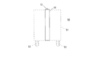
- FIG. 1 shows a configuration in which a chip accumulation state detection apparatus according to an embodiment of the present invention is applied to a chip bucket
- FIG. 2 is a left side view thereof
- FIG. 3 is a right side view thereof.
- the chip bucket 50 includes a housing-like main body 51 having an open upper surface, four wheels 52 fixed to the lower surface of the main body 51, and a handle 53 provided on the right side surface of the main body 51.
- the chip is disposed below a chip discharge port of a chip conveyor (not shown) provided in a machine tool (not shown).
- the chips discharged from the chip discharge port of the chip conveyor are collected in the main body 51 of the chip bucket 50 and accumulated in the main body 51.
- the said chip refers to all things produced by removal processing, and is a concept including a chip-like thing, a curled thing, and a powdery thing.
- the inside of the main body 51 is a chip accumulation region.
- the chip accumulation state detection device 1 includes a light emitting unit 2, a light receiving unit 10, a light source control unit 15, an accumulation state determination unit 16, a reference data storage unit 17, and a display device 18.
- the light emitting unit 2 and the light receiving unit 10 are disposed in the main body 51 so as to face each other, and are appropriately mounted on the main body 51 so as to contact the inner surface of the main body 51.
- a region between the light emitting unit 2 and the light receiving unit 10 in the main body 51 is set as a detection region 55.
- the light source control unit 15, the deposition state determination unit 16, and the reference data storage unit 17 are mounted on one board, and this board is attached to the chip bucket 50.
- the light emitting unit 2 includes an elongated substrate 3 arranged along the vertical direction, two light sources L1 and L2 provided on the substrate 3, a connector 4 provided on the upper end of the substrate 3,
- the substrate 3 is provided with a transparent and liquid-tight container 5 that accommodates the substrate 3 provided with the two light sources L1 and L2 in a state where the connector 4 protrudes upward.
- wirings connected to the light sources L ⁇ b> 1 and L ⁇ b> 2 are formed, and the other ends of the wirings are connected to the connector 4.
- each of the light sources L1 and L2 includes an LED, the light source L1 is provided near the upper edge of the detection region 55, and the light source L2 is provided near the middle in the height direction of the detection region 55. Yes.
- the light receiving unit 10 includes an elongated substrate 11 that is also disposed along the vertical direction, and seven illuminance sensors S1 to S7 disposed on the substrate 11 at equal intervals along the vertical direction.
- the connector 12 provided at the upper end of the substrate 11 and the substrate 11 provided with the illuminance sensors S1 to S7 are composed of a transparent and liquid-tight container 13 that accommodates the connector 12 protruding upward.
- the uppermost illuminance sensor S1 is provided near the upper edge of the detection area 55, and the lowermost illuminance sensor S7 is provided slightly above the lower edge of the detection area 55.
- the light sources L1 and L2 and the illuminance sensors S1 to S7 are provided so that the light irradiation side of the light sources L1 and L2 and the light receiving side of the illuminance sensors S1 to S7 face each other. It has been.
- the illuminance sensors S1 to S7 output a signal corresponding to the amount of received light, and can be applied to those composed of a phototransistor or a photodiode.
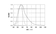
- a phototransistor having a sensitivity characteristic close to human visibility characteristics was used.
- FIG. 4 shows the relationship between the wavelength of light and the relative sensitivity.
- the solid line shows the characteristics of the illuminance sensors S1 to S7, and the broken line shows the characteristics of a person.
- FIG. 5 shows relative sensitivity characteristics according to the angle of incident light of the illuminance sensors S1 to S7.
- the angle 0 degree is the front of the illuminance sensors S1 to S7.
- the illuminance sensors S1 to S7 exhibit high sensitivity to light whose light receiving direction is within a certain angle (for example, within 20 degrees) from the front, and provide a certain degree of directivity to the light receiving sensitivity.
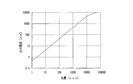
- FIG. 6 shows output characteristics of the illuminance sensors S1 to S7 of this example.
- the illuminance sensors S1 to S7 in this example output current as shown in FIG. 6 according to the amount of received light.
- the light source control unit 15 has a battery as appropriate, and is connected to the light sources L1 and L2 on the substrate 3 via the connector 4, and supplies power to the light sources L1 and L2, respectively.
- L1 and L2 are turned on, that is, light is emitted from the light sources L1 and L2.
- the light sources L1 and L2 are made of LEDs, and the light emitted from the light sources L1 and L2 does not have directivity like laser light, and is irradiated to the surroundings in a diffused state to some extent.
- the light source control unit 15 turns on the light sources L1 and L2 in addition to a mode in which these light sources are alternatively turned on, and a mode in which both are turned on simultaneously. .
- the accumulation state determination unit 16 is connected to the illuminance sensors S1 to S7 on the substrate 11 via the connector 12, and outputs signals (current signals) output from the illuminance sensors S1 to S7. Each is received, and the accumulation state of the chips in the main body 51, that is, in the accumulation region is determined.
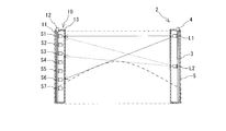
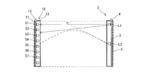
- the chip accumulation state is the state shown in FIG. 7, if only the light source L1 is turned on, the illuminance sensors S1 to S6 above the illuminance sensors S1 to S6 are removed except for the illuminance sensor S7 buried in the accumulated chips. Irradiation light from L1 is received (see solid line arrows shown in FIG. 7). From the sensitivity characteristics of the illuminance sensors S1 to S7 shown in FIG. 5, the amount of light received by the illuminance sensor S1 located in front of the light source L1 is the largest. The amount of light received by the sensor S6 is the smallest.
- the output value from the illuminance sensor S1 is the largest, and the output value decreases in the order of the illuminance sensors S2, S3, S4, S5, and S6.
- Such output signals are input to the accumulation state determination unit 16 from the illuminance sensors S1, S2, S3, S4, S5, and S6, respectively.
- the illumination light from the light source L2 is not received by the illuminance sensor S7 buried in the chips.
- the upper illuminance sensors S1 to S3 receive the irradiation light from the light source L2 without being blocked by the chips.
- the illuminance sensors S4 to S6 below the illuminance sensor S3 the irradiation light from the light source L2 is blocked by the chips, so that the irradiation light is not directly received, and the scattered light scattered around is small. Is received.
- the amount of light received by the illuminance sensor S3 close to the front of the light source L2 among the illuminance sensors S1 to S3 that directly receive the light emitted from the light source L2.
- the amount of light received is the largest, and the light receiving amount decreases in order.
- the illuminance sensors S4 to S6 that receive a small amount of scattered light
- the light reception amount of the uppermost illuminance sensor S4 is large, and the light reception amount decreases in sequence as it is located below this. Then, such output signals are input to the accumulation state determination unit 16 from the illuminance sensors S1, S2, S3, S4, S5, and S6, respectively.
- the accumulation state determination unit 16 outputs the output values of the illuminance sensors S1 to S7 that are input when only the light source L1 is lit, and the illuminance sensors S1 to S7 that are input when only the light source L2 is lit.
- the chip accumulation state is determined from the output value of S7. That is, when only the light source L1 is lit, relatively large output values are input from the illuminance sensors S1 to S6, while when only the light source L2 is lit, relatively large output values are output from the illuminance sensors S1 to S3.
- the chip accumulation state is a mountain shape, and further, the highest output value is input from the illuminance sensor S3 with only the light source L2 turned on, so that the top of the deposit Is near the height position of the illuminance sensor S3.
- the chip can be determined according to the determination criteria as described above as long as the chip is in a state where chips are accumulated so that the irradiation light from the light source L2 is received by at least the illuminance sensor S1.
- the accumulation state determination unit 16 determines that the chips are accumulated above the light source L2.
- the tops of the accumulated chips are estimated from the output values of the illuminance sensors S1 to S7 inputted with only the light source L1 turned on.
- the accumulation state determination unit 16 is configured such that the accumulated chips are located near the lowest illuminance sensor S2 among the illuminance sensors S1 and S2 that directly receive the light emitted from the light source L2. It is determined that there is a top.
- the value differs depending on the chip deposition state, that is, the deposition shape such as flat deposition or mountain deposition, and the position of the top of the deposit. Therefore, the accumulation state determination unit 16 outputs the output values of the illuminance sensors S1 to S7 that are input with only the light source L1 lit, and the illuminance sensors that are input with only the light source L2 lit.
- the chip accumulation state can be determined based on the output values of S1 to S7.
- the correlation with the deposition state (that is, the deposition shape such as flat or mountain-shaped deposition, the position of the top of the deposit, etc.) can be obtained empirically in advance. Therefore, in this example, the data (correlation data) related to the correlation acquired empirically in this way is stored in the reference data storage unit 17, and the deposition state determination unit 16 turns on only the light source L1.
- the reference data storage is based on the output values of the illuminance sensors S1 to S7 that are input in a state of being turned on, and the output values of the illuminance sensors S1 to S7 that are input in the state of turning on only the light source L2.
- the accumulated state of chips is determined with reference to the correlation data stored in the unit 17.
- the deposition state determination unit 16 transmits data related to the determination result executed as described above to the display device 18 via wireless or wired, and causes the display device 18 to display the determination result.
- the display device 18 may be unique, it is preferable to use the display attached to the machine tool because it is easy for the operator to confirm. As a display mode, it may be displayed as text information or a display using a figure or the like, but a display capable of alerting the operator according to the accumulation state is preferable.
- the chip bucket 50 to which the chip accumulation state detection device 1 is mounted is provided on a chip conveyor (not shown). Chips that are disposed below the chip discharge port of the chip conveyor and are discharged from the chip discharge port of the chip conveyor are collected in the main body 51 of the chip bucket 50 and accumulated in the main body 51.
- the chip accumulation state in the chip bucket 50 is detected regularly or irregularly by the chip accumulation state detection device 1. That is, under the control of the light source control unit 15, only the light source L1 is turned on, and in this state, output signals output from the illuminance sensors S1 to S7 are input to the deposition state determination unit 16, and only the light source L2 is turned on. In this state, an output signal output from each of the illuminance sensors S1 to S7 is input to the deposition state determination unit 16, and the deposition state determination unit 16 outputs from the input illuminance sensors S1 to S7. Based on the value, the correlation data stored in the reference data storage unit 17 is referred to, and the chip accumulation state (the chip accumulation shape, the top position of the deposit, etc.) is determined. The result determined by the accumulation state determination unit 16 is displayed on the display device 18.
- the operator can confirm the chip accumulation state in the chip bucket 50 by confirming the determination result displayed on the display device 18.
- the chip bucket 50 can be selected according to the accumulation state. It is possible to take measures such as exchanging and scraping the chips.
- the chip bucket 50 is replaced with another one, the board on which the light source control unit 15, the deposition state determination unit 16, and the reference data storage unit 17, the light emitting unit 2, and the light receiving unit 10 are replaced before replacement. Are attached to a new chip bucket 50 after replacement.
- the chip accumulation state detection device 1 of the present example since the light source (light emitting unit) that irradiates straight light is not used unlike the conventional chip detection device, the above-described problem relating to erroneous detection does not occur.
- the detection light can pass through the curled chip space.
- the chip accumulation state detection device 1 of this example the light emitted from the light sources L1 and L2 is diffused light, so that the irradiation light passes through the curled chip space. Even if the light passes through, the amount of light received by the illuminance sensors S1 to S7 is very small. It will not be judged.
- illuminance sensors S1 to S7 arranged in a line are provided, but the number of illuminance sensors is not limited, and may be more or less than this. If the accumulation state of chips can be detected, only one illuminance sensor may be provided. If there is nothing between the light source and the illuminance sensor that blocks the light emitted from the light source, the illuminance sensor receives the maximum amount of light, and a signal with a value corresponding thereto is output from the illuminance sensor.
- the illuminance sensors may be provided in double rows and double columns. If it does in this way, the various accumulation state of chips can be judged from the output value of the illuminance sensor arranged in double rows and double columns.
- the two light sources L1 and L2 are provided, but the number of light sources to be provided is not limited, and may be more or less than this. If the accumulated state of chips can be detected, only one light source may be provided. Alternatively, as shown in FIG. 9, seven light sources L1 to L7 may be provided to face the illuminance sensors S1 to S7, respectively. In this case, it is preferable that the light source control unit 15 is configured to selectively supply power to the light sources L1 to L7 to light them. In this way, various accumulation states of chips can be determined. Further, the light sources may be provided in double rows and double columns.
- the accumulation state determination unit 16 determines that the accumulation state is determined when a value of an output signal received from the illuminance sensor S1 when the light sources L1 and L2 are turned off is equal to or less than a predetermined reference value.
- the determination process may be executed.
- disturbance light may exist in addition to the light emitted from the light sources L1 and L2, and in this case, the disturbance light is received by the illuminance sensors S1 to S7. Then, the output value from the illuminance sensors S1 to S7 increases by the amount of the disturbance light, and the accumulation state determination unit 16 cannot perform accurate determination.
- the accumulation state determination unit 16 determines the chip accumulation state, so that an accurate determination that is not affected by ambient light can be performed.
- the illuminance sensor for determining whether or not ambient light is present is preferably the uppermost illuminance sensor S1 that is not easily affected by the accumulation state of chips, but is not limited thereto.
- the accumulation state determination unit 16 receives the value of the output signal received from the illuminance sensor S1 when the light sources L1 and L2 are turned off and the illuminance sensor S1 when the light source L1 is turned on.
- the deposition state determination process may be executed.
- the illuminance sensor for determining whether or not ambient light is present is preferably the uppermost illuminance sensor S1 that is not easily affected by the state of chip accumulation, but is not limited thereto.
- the chip accumulation state detection device 1 is applied to the chip bucket 50.
- the present invention is not limited to this, and the chip accumulation state detection device 1 is disposed in the machining area of the machine tool. You may make it monitor the accumulation state of the chip in an area
- erroneous detection is likely to occur due to the influence of the coolant mist and fine chips.
- the light source L1 even if the coolant mist and fine chips exist, the light source L1.
- L2 are scattered by these and received by the illuminance sensors S1 to S7, so that the illuminance sensors S1 to S7 are not affected by the coolant mist or fine chips, and the light from the light sources L1 and L2 Is received. Therefore, in this chip accumulation state detection apparatus 1, erroneous detection as in the prior art does not occur.
- the chip accumulation state detection device 1 is disposed in the chip input portion of the chip conveyor, and the chip accumulation state detection device 1 provides a predetermined amount of chips. Power consumption can be reduced by driving the chip conveyor only when necessary, such as driving the chip conveyor and discharging chips when it is detected that .
- the chip accumulation state detection device 1 may be disposed in the middle of the chip conveyor conveyance path to detect the chip conveyance state. In the case where chips are not detected by the chip accumulation state detection device 1 even though the removal processing is executed by the machine tool and the chip conveyor is driven, the chips are clogged in the conveying path of the chip conveyor. There is a possibility, and in such a case, by appropriately issuing an alarm to the operator, it is possible to take appropriate measures such as removing clogged chips.
Landscapes
- Engineering & Computer Science (AREA)
- Mechanical Engineering (AREA)
- Physics & Mathematics (AREA)
- Optics & Photonics (AREA)
- Machine Tool Sensing Apparatuses (AREA)
- Photometry And Measurement Of Optical Pulse Characteristics (AREA)
- Geophysics And Detection Of Objects (AREA)
Abstract
対象物が嵩高い切屑堆積物でも、また、クーラントミストや微細な切屑が浮遊する環境下でも、正確に堆積状態を検出するこができる検出装置を提供する。切屑の堆積領域内に設定された検出領域を挟み、互いに対峙するように配設された、拡散光を照射する少なくとも一つの光源(L1,L2)、及び受光光量に応じた信号を出力する少なくとも一つの照度センサ(S1~S7)と、光源(L1,L2)に電力を供給して光を照射させる光源制御部(15)と、照度センサ(S1~S7)から出力された信号を受信して、堆積領域内における切屑の堆積状態を判定する堆積状態判定部(16)とを備える。
Description
本発明は、工作機械の除去加工によって生じる切屑の堆積状態を検出する検出装置に関する。
工作機械の分野では、その加工領域内において、工具などを用いた各種材料の除去加工が行われ、その結果として切屑が生じる。そして、従来の一般的な態様では、生じた切屑は、その一部が、加工領域内のテーブルなどに堆積されるものの、その殆どはチップコンベアなどの適宜排出装置によって機外のチップバケット等に排出される。
そして、このような切屑処理において、例えば、チップバケットに回収される切屑が当該チップバケットから溢れると、周囲に切屑が飛散する為、チップバケットから切屑が溢れる前にこれを検出して、オペレータに報知するなどの処置を講じる必要がある。
また、加工中の加工領域内(例えば、テーブル上)に切屑が多量に堆積される場合には、工具の加工作用領域からの切屑の排出がスムーズに行われないという問題や、逆に加工作用領域内に切屑が侵入するといった問題を生じ、結果、良好な加工精度が得られないという問題を生じる。したがって、加工領域内における切屑の堆積状態を検出し、加工に支障が生じる程度に切屑が堆積された場合には、これをオペレータに報知するのが好ましい。
このような切屑検出装置として、従来、特開2003-145388号公報(下記特許文献1)に開示された装置が知られている。この切屑検出装置は、加工領域を画定する密閉カバーの周囲に、複数組の発光部及び受光部を対向配置させた構成を備え、発光部から照射された直進光(一般的にはレーザ光)を受光部によって受光するように構成されている。切屑が堆積すると、この切屑により直進光が遮られて、受光部に届かなくなるため、受光部が受光できなくなったときに、切屑が堆積したと判定することができる。また、複数組の光部及び受光部に高低差を設けることで、切屑の3次元的な堆積状態を把握することができるとのことである。
ところが、上述した従来の切屑検出装置には、以下に説明するような問題があった。
即ち、まず、上記従来の切屑検出装置は、発光部として、直進光(一般的にはレーザ光)を照射するものを用いているため、誤検出を生じ易いという問題がある。切屑の形状は、被加工物の材質、工具の種類やその形状等によって様々であり、その中に、カールした形状を有する切屑がある。このような切屑の堆積物は、そのカール形状によって嵩高くなっており、多くの空間を有している。したがって、従来の切屑検出装置では、発光部と受光部との間に切屑の堆積物が存在しているにも拘らず、発光部から照射された直進光が前記空間部を抜け通って受光部に達するといったことが起こり、このため、受光部によって切屑が検出されないという問題を生じ得るのである。
即ち、まず、上記従来の切屑検出装置は、発光部として、直進光(一般的にはレーザ光)を照射するものを用いているため、誤検出を生じ易いという問題がある。切屑の形状は、被加工物の材質、工具の種類やその形状等によって様々であり、その中に、カールした形状を有する切屑がある。このような切屑の堆積物は、そのカール形状によって嵩高くなっており、多くの空間を有している。したがって、従来の切屑検出装置では、発光部と受光部との間に切屑の堆積物が存在しているにも拘らず、発光部から照射された直進光が前記空間部を抜け通って受光部に達するといったことが起こり、このため、受光部によって切屑が検出されないという問題を生じ得るのである。
また、工作機械を用いた一般的な加工分野では、加工部位の冷却や切削抵抗の軽減を目的としてクーラントが用いられており、その加工領域内では、クーラントがミスト状になって浮遊し、また、微細な切屑、例えば、粉状の切屑が浮遊している。したがって、上述した従来の切屑検出装置をこの加工領域内に設置すると、発光部から照射された直進光がクーラントミストや微細な切屑によって遮られるといったことが起こり、この場合には、逆に、切屑が堆積していないにも拘らず、切屑が堆積していると誤検出されるという問題を生じる。
更に、従来の切屑検出装置の前記発光部及び受光部は、物体の有無しか判別することができない、言い換えれば2値的な判別しかできないため、切屑の堆積形状を含めた堆積状態を判別できないという問題があり、また、前記発光部及び受光部が、前記クーラントミストや微細な切屑によって少しでも汚損されると、正確な判定ができなくなるという問題もある。
本発明は、以上の実情に鑑みなされたものであって、カール形状を有するなど、嵩高い切屑の堆積物であっても正確にその堆積状態を検出することができるとともに、クーラントミストや微細な切屑が浮遊する加工領域内でも、切屑の堆積状態を正確に検出することができる検出装置の提供を、その目的とする。
上記課題を解決するための本発明は、工作機械の除去加工によって生じた切屑の堆積状態を検出する装置であって、
前記切屑の堆積領域内に設定された検出領域を挟み、互いに対峙するように配設された、拡散光を照射する少なくとも一つの光源、及び受光光量に応じた信号を出力する少なくとも一つの照度センサと、
前記光源に電力を供給して光を照射させる光源制御部と、
前記照度センサから出力された信号を受信して、前記堆積領域内における前記切屑の堆積状態を判定する堆積状態判定部とを備えた切屑堆積状態検出装置に係る。
前記切屑の堆積領域内に設定された検出領域を挟み、互いに対峙するように配設された、拡散光を照射する少なくとも一つの光源、及び受光光量に応じた信号を出力する少なくとも一つの照度センサと、
前記光源に電力を供給して光を照射させる光源制御部と、
前記照度センサから出力された信号を受信して、前記堆積領域内における前記切屑の堆積状態を判定する堆積状態判定部とを備えた切屑堆積状態検出装置に係る。
この切屑堆積状態検出装置によれば、まず、少なくとも一つの光源と、少なくとも一つの照度センサとを、切屑堆積領域内に適宜設定された検出領域を挟んで互いに対峙するように配設した後、前記光源制御部による制御の下で、前記光源から光を照射させる。
前記照度センサは、受光量に応じた信号、例えば電流などを出力するもので、フォトトランジスタ、或いはフォトダイオードなどから構成される。また、前記光源は拡散光を照射するもので、一般的な電球、蛍光灯、LEDなどを適用することができる。尚、この点において、レーザ光のような指向性を有する光を照射する従来の発光部とは、その構成が異なる。また、当然のことながら、前記光源から照射される光の波長は、前記照度センサが感知し得る波長である必要があり、最も感度の高い波長であるのが好ましい。
前記光源と照度センサとの間に、光源から照射された光を遮るものが無ければ、照度センサには最大の光量が受光され、それに応じた値の信号が照度センサから出力される。一方、前記検出領域内で、前記光源と照度センサとの間に切屑が徐々に堆積されると、その堆積量に応じて、徐々に前記照度センサに受光される光量が減少していき、照度センサから出力される信号の値(出力値)も減少して行く。そして、遂には、前記照度センサに受光される光量が殆ど無くなり、当該照度センサからの出力値も最小となる。
前記堆積状態判定部は、切屑の堆積状態に応じて変化する照度センサからの出力値を基に、前記堆積領域内における前記切屑の堆積状態を判定する。尚、前記切屑の堆積状態と照度センサからの出力値との相対的な関係を予め経験的に求めておき、前記堆積状態判定部では、照度センサから出力される現在の出力値と、経験的に得られた前記相対関係から、切屑の堆積状態を判定するようにした態様を採ることができる。尚、本発明における前記切屑は、除去加工によって生じるあらゆるものを指し、チップ状のもの、カールしたものや粉状のものを含む概念である。
このように、この切屑堆積状態検出装置によれば、従来の切屑検出装置のように、直進光を照射する光源(発光部)を用いていないので、上述した誤検出に関する問題を生じない。例えば、従来の切屑検出装置では、発光部から照射される直進光が受光部で受光されるか否かというON,OFFの判断であるため、カールした切屑の空間部を検出光が抜け通ることによる誤検出を生じ易いが、この切屑堆積状態検出装置では、光源から照射される拡散光が照度センサに受光される受光量であって、切屑の堆積状態に応じて連続的に変化する受光量を基に切屑の堆積状態を判定しているので、上述した誤検出を生じ難い。
また、従来の切屑検出装置では、クーラントミストや微細な切屑の影響を受けて誤検出を生じ易いが、この切屑堆積状態検出装置では、クーラントミストや微細な切屑が存在しても、光源からの光はこれらによって散乱されて照度センサに受光されるため、照度センサには、クーラントミストや微細な切屑の影響を受けることなく、光源からの光が受光される。したがって、この切屑堆積状態検出装置では、従来のような誤検出は生じ難い。
尚、この切屑堆積状態検出装置では、前記照度センサは、その複数個が上下方向に沿って1列に配設されているのが好ましい。このようにすれば、上下方向に配設された各照度センサからの出力値を基に、切屑の堆積状態を判定することができるので、より正確な判定を行うことができる。
また、前記切屑堆積状態検出装置において、前記光源は、その複数個が上下方向に沿って1列に配設されているのが好ましい。このようにすれば、各光源から照射された光が、照度センサによって受光される光量は、切屑の堆積状態に応じて、より明確に変化する為、より正確に、切屑の堆積状態を判定することができる。
また、この場合に、前記光源制御部は、複数の光源に対し、択一的に電力を供給して光を照射させるように構成され、
前記堆積状態判定部は、前記各光源から照射される光の受光状態に応じて前記照度センサから出力される信号を基に、前記堆積領域内における前記切屑の堆積状態を判定するように構成されていても良い。
前記堆積状態判定部は、前記各光源から照射される光の受光状態に応じて前記照度センサから出力される信号を基に、前記堆積領域内における前記切屑の堆積状態を判定するように構成されていても良い。
この切屑堆積状態検出装置によれば、複数の光源に対して前記光源制御部から択一的に電力が供給されて当該光源から光が照射され、前記堆積状態判定部では、各光源から照射される光の受光状態に応じて前記照度センサから出力される信号を基に、切屑の堆積状態が判定される。切屑が前記堆積領域内に徐々に投入されて堆積される場合、大抵、切屑は山形に堆積される。この場合に、上下方向に沿って配設された光源から択一的に光を照射させると、切屑の堆積形状によって、照度センサに受光される光量が大きく異なる。したがって、この構成によれば、切屑の堆積形状を含んだ堆積状態を判別することができる。
また、上記の切屑堆積状態検出装置において、前記堆積状態判定部は、前記光源の消灯時に前記照度センサから受信される出力信号の値が、予め定めた基準値以下である場合に、前記堆積状態の判定を実行するように構成されていても良い。
切屑堆積状態検出装置が配設される環境では、上記光源から照射される光以外に外乱光が存在する場合があり、この場合に、外乱光が照度センサに受光されると、この外乱光の分だけ照度センサからの出力値が増加することになり、このため前記堆積状態判定部では正確な判定ができなくなる。そこで、光源の消灯時に照度センサから出力される出力値が、予め定めた基準値以下である場合、即ち、影響の有る外乱光を照度センサが受光していないと判断された場合に、前記堆積状態判定部によって切屑の堆積状態を判定するようにすることで、外乱光の影響を受けない正確な判定を行うことができる。
また、上記の切屑堆積状態検出装置において、前記堆積状態判定部は、前記光源の消灯時に前記照度センサから受信される出力信号の値と、前記光源の点灯時に前記照度センサから受信される出力信号の値との差分が、予め定めた基準値以上である場合に、前記堆積状態の判定を実行するように構成されていても良い。
光源の消灯時に照度センサから出力される出力値と、光源の点灯時に照度センサから出力される出力値との差分を取ることで、照度センサに外乱光が受光されているかどうかを判別することができる。即ち、照度センサに外乱光が受光されている場合には、光源の消灯時に照度センサから出力される出力値が、外乱光の無い場合に比べて大きな値であるため、光源の消灯時と点灯時とにおける照度センサからの出力値の差分が、予め定めた基準値以上である場合には、照度センサが影響の有る外乱光を受光していないと判断することができ、この場合に、堆積状態判定部によって切屑の堆積状態を判定するようにすることで、外乱光の影響を受けない正確な判定を行うことができる。
以上のように、本発明に係る切屑堆積状態検出装置によれば、従来の切屑検出装置のように、直進光を照射する光源(発光部)を用いていないので、上述した従来装置における誤検出の問題を生じない。
また、前記照度センサの複数個を上下方向に沿って1列に配設すれば、上下方向に配設された各照度センサからの出力値を基に、切屑の堆積状態を判定することができるので、切屑の堆積状態をより正確に判定することができる。
また、前記光源の複数個を上下方向に沿って1列に配設すれば、各光源から照射され、照度センサによって受光される光量が、切屑の堆積状態に応じてより明確に変化する為、より正確に切屑の堆積状態を判定することができる。
また、この場合に、光源制御部が、複数の光源に対し択一的に電力を供給して光を照射させ、堆積状態判定部が、各光源から照射される光の受光状態に応じて照度センサから出力される信号を基に、切屑の堆積状態を判定するようにすれば、切屑の堆積形状を含んだ堆積状態を判別することができる。
更に、光源の消灯時に照度センサから出力される出力値が、予め定めた基準値以下である場合、或いは、光源の消灯時と点灯時とにおける照度センサからの出力値の差分が、予め定めた基準値以上である場合に、堆積状態判定部によって堆積状態の判定を実行するようにすれば、外乱光の影響を受けない正確な判定を行うことができる。
以下、本発明の具体的な実施の形態について、図面を参照しながら説明する。図1は、本発明の一実施形態に係る切屑堆積状態検出装置をチップバケットに適用した構成を示しており、図2は、その左側面図であり、図3は、右側面図である。
このチップバケット50は、上面が開口した筐体状の本体51と、この本体51の下面に固設された4つの車輪52と、本体51の右側面に設けられた取手53とからなり、例えば、工作機械(図示せず)に設けられたチップコンベア(図示せず)の切屑排出口の下方に配置される。斯くして、チップコンベアの切屑排出口から排出された切屑が、チップバケット50の本体51内に回収され、当該本体51内に堆積される。尚、本例において、前記切屑は、除去加工によって生じるあらゆるものを指し、チップ状のもの、カールしたものや粉状のものを含む概念である。また、言うまでもなく、この例では本体51内が切屑堆積領域となる。
一方、切屑堆積状態検出装置1は、発光部2、受光部10、光源制御部15、堆積状態判定部16、基準データ記憶部17及び表示装置18からなる。前記発光部2及び受光部10は、相互に対向するように本体51内に配設され、それぞれ本体51の内側面に当接するように、当該本体51に適宜装着されている。尚、本体51内の、前記発光部2と受光部10との間の領域が検出領域55に設定される。また、光源制御部15、堆積状態判定部16及び基準データ記憶部17は一つのボードに搭載され、このボードがチップバケット50に取り付けられる。
前記発光部2は、上下方向に沿って配設された細長い基板3と、この基板3上に設けられた2つの光源L1,L2と、基板3の上端部に設けられたコネクタ4と、この2つの光源L1,L2が設けられた基板3を、前記コネクタ4が上方に突出した状態で収納する透明且つ液密状の容器5からなる。前記基板3には、前記光源L1,L2にそれぞれ接続する配線が形成されており、この配線の他端が前記コネクタ4に接続されている。本例では、前記光源L1,L2は、それぞれLEDから構成され、光源L1が前記検出領域55の上縁部付近に設けられ、光源L2が前記検出領域55の高さ方向中間付近に設けられている。
前記受光部10は、同じく上下方向に沿って配設された細長い基板11と、この基板11上に、その上下方向に沿って等間隔に配設された7個の照度センサS1~S7と、基板11の上端部に設けられたコネクタ12と、照度センサS1~S7が設けられた基板11を、前記コネクタ12が上方に突出した状態で収納する透明且つ液密状の容器13からなる。前記基板11には、前記照度センサS1~S7にそれぞれ接続する配線が形成されており、この配線の他端が前記コネクタ12に接続されている。また、最上位の照度センサS1は、前記検出領域55の上縁部付近に設けられ、最下位の照度センサS7は、前記検出領域55の下縁部より少し上方に設けられている。
斯くして、前記光源L1,L2と前記照度センサS1~S7とは、前記光源L1,L2の光を照射する側と、前記照度センサS1~S7の受光側とが、互いに対峙するように設けられている。
前記照度センサS1~S7は、受光光量に応じた信号を出力するもので、フォトトランジスタ、或いはフォトダイオードなどから構成されるものを適用することができるが、本例では、図4に示すように、人の視感度特性に近い感度特性を有するフォトトランジスタから構成されるものを用いた。尚、図4は、光の波長と相対感度との関係を示しており、実線が照度センサS1~S7の特性を示し、破線が人の特性を示している。
また、図5に、この照度センサS1~S7の入射光の角度に応じた相対感度特性を示している。角度0度は照度センサS1~S7の正面である。同図5に示すように、この照度センサS1~S7は、受光方向が正面からある角度以内(例えば20度以内)の光に対して高い感度を示しており、受光感度にある程度の指向性を有している。また、図6に、本例の照度センサS1~S7の出力特性を示している。本例の照度センサS1~S7は、受光光量に応じて、図6に示すような、電流を出力する。
前記光源制御部15は、適宜バッテリを有するとともに、前記コネクタ4を介して、前記基板3上の光源L1,L2にそれぞれ接続されており、これら光源L1,L2に電力を供給して、当該光源L1,L2を点灯させる、即ち、当該光源L1,L2から光を照射させる。上述したように、光源L1,L2はLEDからなり、当該光源L1,L2から照射される光はレーザ光のような指向性を有しておらず、ある程度拡散した状態で周囲に照射される。尚、この光源制御部15によって光源L1,L2を点灯させる態様は、これらを択一的に点灯させる態様の他、両方を同時に点灯させる態様があり、当然のことながら両者を消灯させる態様もある。
また、前記堆積状態判定部16は、前記コネクタ12を介して、前記基板11上の照度センサS1~S7にそれぞれ接続されており、各照度センサS1~S7から出力される信号(電流信号)をそれぞれ受信して、前記本体51内、即ち、堆積領域内における前記切屑の堆積状態を判定する。
切屑の堆積状態が図7に示した状態である場合に、光源L1のみを点灯させると、堆積された切屑に埋没している照度センサS7を除き、これより上方の照度センサS1~S6に光源L1からの照射光が受光される(図7に示した実線の矢印を参照)。図5に示した照度センサS1~S7の感度特性からして、光源L1の正面に位置する照度センサS1の受光光量が最も多く、これより下に位置するものほど順に受光量が少なくなり、照度センサS6の受光量が最も少ない。したがって、照度センサS1からの出力値が最も大きく、照度センサS2、S3、S4、S5、S6の順に出力値が小さくなる。堆積状態判定部16には、照度センサS1、S2、S3、S4、S5、S6から、このような出力信号がそれぞれ入力される。
次に、光源L1を消灯させて、光源L2のみを点灯させると、同様に、切屑に埋没している照度センサS7には、光源L2からの照射光は受光されない。そして、切屑に埋没していない照度センサS1~S6のうち、上方の照度センサS1~S3には、光源L2からの照射光が切屑によって遮られることなく受光される。一方、照度センサS3より下方の照度センサS4~S6については、光源L2からの照射光が切屑によって遮られるため、当該照射光が直接受光されることはなく、周囲で散乱された散乱光が僅かに受光される。斯くして、図7に示した状態で光源L2を点灯させると、光源L2からの照射光が直接受光される照度センサS1~S3の内、光源L2の正面に近い照度センサS3の受光光量が最も多く、これより上に位置するものほど順に受光量が少なくなる。一方、僅かな散乱光が受光される照度センサS4~S6については、最も上位の照度センサS4の受光量が多く、これより下に位置するものほど順に受光量が少なくなる。そして、堆積状態判定部16には、照度センサS1、S2、S3、S4、S5、S6から、このような出力信号がそれぞれ入力される。
前記堆積状態判定部16は、光源L1のみを点灯させた状態で入力される前記各照度センサS1~S7の出力値と、光源L2のみを点灯させた状態で入力される前記各照度センサS1~S7の出力値とから、切屑の堆積状態を判定する。即ち、光源L1のみを点灯させた状態では、照度センサS1~S6から比較的大きな出力値が入力される一方、光源L2のみを点灯させた状態では、照度センサS1~S3から比較的大きな出力値が入力されることから、切屑の堆積状態が山形であることが判別され、更に、光源L2のみを点灯させた状態で照度センサS3から最も大きな出力値が入力されることから、堆積物の頂部が照度センサS3の高さ位置付近にあることが分かる。
図7に示すように、光源L2からの照射光が少なくとも照度センサS1によって受光されるような切屑の堆積状態であれば、以上のような判定基準によって判定することができるが、図8に示すように、切屑の堆積が増えて、光源L2からの照射光が照度センサS1にも受光されない状態であれば、前記堆積状態判定部16は、切屑が光源L2より上方に堆積していると判断するとともに、光源L1のみを点灯させた状態で入力される前記各照度センサS1~S7の出力値から、堆積された切屑の頂部を推定する。図8に示した例では、前記堆積状態判定部16は、光源L2からの照射光が直接受光される照度センサS1,S2の内、最も下に位置する照度センサS2の付近に、堆積切屑の頂部が在ると判定する。
以上のように、光源L1のみを点灯させた状態で出力される前記各照度センサS1~S7の出力値と、光源L2のみを点灯させた状態で出力される前記各照度センサS1~S7の出力値とは、切屑の堆積状態、即ち、平坦な堆積か或いは山形の堆積かといった堆積形状や、堆積物の頂部の位置に応じて異なったものとなる。したがって、前記堆積状態判定部16は、光源L1のみを点灯させた状態で入力される前記各照度センサS1~S7の出力値と、光源L2のみを点灯させた状態で入力される前記各照度センサS1~S7の出力値とを基に、切屑の堆積状態を判定することができる。
光源L1のみを点灯させた状態で出力される前記各照度センサS1~S7の出力値、並びに光源L2のみを点灯させた状態で出力される前記各照度センサS1~S7の出力値と、切屑の堆積状態(即ち、平坦な堆積か或いは山形の堆積かといった堆積形状や、堆積物の頂部の位置等)との相関関係は、予め経験的に取得することができる。したがって、本例では、このように経験的に取得された相関関係に係るデータ(相関データ)を前記基準データ記憶部17に格納しておき、前記堆積状態判定部16は、光源L1のみを点灯させた状態で入力される前記各照度センサS1~S7の出力値、並びに光源L2のみを点灯させた状態で入力される前記各照度センサS1~S7の出力値とを基に、前記基準データ記憶部17に格納した相関データを参照して切屑の堆積状態を判定する。
前記堆積状態判定部16は、上記のようにして実行した判定結果に係るデータを無線又は有線を介して表示装置18に送信して、当該表示装置18に判定結果を表示させる。表示装置18は独自のものでも良いが、工作機械に付設されているディスプレイを兼用するのが、オペレータが確認し易くて好ましい。表示態様としては、テキスト情報として表示しても、図形等を用いた表示としても良いが、堆積状態に応じてオペレータに注意喚起可能な表示が好ましい。
以上の構成を備えた本例の切屑堆積状態検出装置1によれば、当該切屑堆積状態検出装置1が装着されたチップバケット50が、工作機械(図示せず)に設けられたチップコンベア(図示せず)の切屑排出口の下方に配置され、チップコンベアの切屑排出口から排出された切屑が、チップバケット50の本体51内に回収され、当該本体51内に堆積される。
そして、チップバケット50内に堆積される切屑の堆積状態が、切屑堆積状態検出装置1によって定期的又は不定期的に検出される。即ち、光源制御部15による制御の下で、光源L1のみを点灯させ、この状態で各照度センサS1~S7から出力される出力信号を前記堆積状態判定部16に入力するとともに、光源L2のみを点灯させ、この状態で各照度センサS1~S7から出力される出力信号を前記堆積状態判定部16に入力して、当該堆積状態判定部16において、入力された各照度センサS1~S7からの出力値を基に、前記基準データ記憶部17に格納した相関データが参照されて、切屑の堆積状態(切屑の堆積形状や、堆積物の頂部の位置等)が判定される。そして、この堆積状態判定部16によって判定された結果が表示装置18に表示される。
斯くして、オペレータは、表示装置18に表示された判定結果を確認することで、チップバケット50内の切屑の堆積状態を確認することができ、その堆積状態に応じて、例えば、チップバケット50の交換や、切屑の掻き慣らし等の対応を採ることができる。尚、チップバケット50を別のものに交換する場合には、光源制御部15、堆積状態判定部16及び基準データ記憶部17が搭載されたボード、並びに発光部2及び受光部10を、交換前のチップバケット50から取り外して、これらを交換後の新たなチップバケット50に装着する。
また、本例の切屑堆積状態検出装置1によれば、従来の切屑検出装置のように、直進光を照射する光源(発光部)を用いていないので、上述した誤検出に関する問題を生じない。例えば、従来の切屑検出装置では、発光部から照射される直進光が受光部で受光されるか否かというON,OFFの判断であるため、カールした切屑の空間部を検出光が抜け通ることによる誤検出を生じ易いが、本例の切屑堆積状態検出装置1では、光源L1,L2から照射される光が拡散光であるため、仮に、カールした切屑の空間部を照射光が抜け通ることがあっても、この抜け通った光が照度センサS1~S7に受光される光量はごく僅かであり、したがって、このような照射光の抜け通りが生じたとしても、堆積状態判定部16において誤判定されることはない。
以上、本発明の一具体的な実施形態について説明したが、本発明が採り得る具体的な態様は、何らこれに限定されるものではない。
例えば、上例では1列に配列した7個の照度センサS1~S7を設けたが、照度センサを設ける個数に制限があるわけではなく、これよりも多くても少なくても良い。切屑の堆積状態を検出することできれば、1個の照度センサを設けるだけでも良い。光源と照度センサとの間に、光源から照射された光を遮るものが無ければ、照度センサには最大の光量が受光され、それに応じた値の信号が照度センサから出力される。一方、光源と照度センサとの間に切屑が徐々に堆積されると、その堆積量に応じて、徐々に照度センサに受光される光量が減少していき、照度センサから出力される信号の値(出力値)も減少して行く。したがって、1個の照度センサを設けるだけでも、その出力値から切屑の堆積状態を判別することができる。また、照度センサを複行複列に設けても良い。このようにすれば、複行複列に配設された照度センサの出力値から、切屑の多様な堆積状態を判定することができる。
また、上例では、2つの光源L1,L2を設けたが、光源を設ける個数に制限があるわけではなく、これよりも多くても少なくても良い。切屑の堆積状態を検出することできれば、1個の光源を設けるだけでも良い。或いは、図9に示すように、照度センサS1~S7にそれぞれ対向させて、7つの光源L1~L7を設けた構成としても良い。この場合に、前記光源制御部15は、光源L1~L7に対し、択一的に電力を供給して点灯させるように構成されているのが好ましい。このようにすれば、切屑の多様な堆積状態を判定することができる。また、光源を複行複列に設けても良い。
また、上例において、前記堆積状態判定部16は、前記光源L1,L2の消灯時に前記照度センサS1から受信される出力信号の値が、予め定めた基準値以下である場合に、前記堆積状態の判定処理を実行するように構成されても良い。前記切屑堆積状態検出装置1が配設される環境では、上記光源L1,L2から照射される光以外に外乱光が存在する場合があり、この場合に、外乱光が照度センサS1~S7に受光されると、この外乱光の分だけ照度センサS1~S7から出力値が増加することになり、堆積状態判定部16において正確な判定ができなくなる。
そこで、光源L1,L2の消灯時に照度センサS1から出力される出力値が、予め定めた基準値以下である場合、即ち、各照度センサS1~S7が影響の有る外乱光を受光していないと判断された場合に、堆積状態判定部16によって切屑の堆積状態を判定するようにすることで、外乱光の影響を受けない正確な判定を行うことができる。尚、外乱光が存在するか否かを判別するための照度センサは、切屑の堆積状態の影響を受け難い最上位の照度センサS1が好ましいがこれに限られるものではない。
また、上例において、前記堆積状態判定部16は、前記光源L1,L2の消灯時に前記照度センサS1から受信される出力信号の値と、前記光源L1の点灯時に前記照度センサS1から受信される出力信号の値との差分が、予め定めた基準値以上である場合に、前記堆積状態の判定処理を実行するように構成されていても良い。光源L1,L2の消灯時に照度センサS1から出力される出力値と、光源L1の点灯時に照度センサS1から出力される出力値との差分を取ることで、各照度センサS1~S7に外乱光が受光されているかどうかを判別することができる。
即ち、照度センサS1~S7に外乱光が受光される環境にある場合には、光源L1,L2の消灯時に照度センサS1から出力される出力値が、外乱光の無い場合に比べて大きな値であるため、光源L1,L2の消灯時と点灯時とにおける照度センサS1からの出力値の差分が、予め定めた基準値以上である場合には、照度センサS1~S7が影響の有る外乱光を受光していないと判断することができ、この場合に、堆積状態判定部によって切屑の堆積状態を判定するようにすることで、外乱光の影響を受けない正確な判定を行うことができる。尚、この場合も、外乱光が存在するか否かを判別するための照度センサは、切屑の堆積状態の影響を受け難い最上位の照度センサS1が好ましいがこれに限られるものではない。
また、上例では、切屑堆積状態検出装置1をチップバケット50に適用したが、これに限られるものではなく、この切屑堆積状態検出装置1を工作機械の加工領域内に配設して当該加工領域内における切屑の堆積状態を監視するようにしても良い。上述した従来の切屑検出装置では、クーラントミストや微細な切屑の影響を受けて誤検出を生じ易いが、この切屑堆積状態検出装置1では、クーラントミストや微細な切屑が存在しても、光源L1,L2からの光はこれらによって散乱されて照度センサS1~S7に受光されるため、照度センサS1~S7には、クーラントミストや微細な切屑の影響を受けることなく、光源L1,L2からの光が受光される。したがって、この切屑堆積状態検出装置1では、従来のような誤検出は生じない。
或いは、前記切屑堆積状態検出装置1をチップコンベアの搬送経路内に配設しても良い。チップコンベアを常時駆動するようにすると、電力の無駄遣いにつながるため、例えば、チップコンベアの切屑投入部に上記切屑堆積状態検出装置1を配設し、当該切屑堆積状態検出装置1によって所定量の切屑が堆積されたことが検出されたときに、チップコンベアを駆動して切屑を排出するというように、適宜必要なときにのみチップコンベアを駆動するようにすれば、省電力化を図ることができる。
或いは、チップコンベアの搬送経路の途中に上記切屑堆積状態検出装置1を配設して、切屑の搬送状態を検出するようにしても良い。工作機械で除去加工が実行され、且つチップコンベアが駆動されているにもかかわらず、切屑堆積状態検出装置1によって切屑が検出されない場合には、チップコンベアの搬送路の途中で切屑が詰まっている可能性があり、このような場合に適宜オペレータに警報を発することで、詰まった切屑を除去するなど、適切な処置を講じることができる。
1 切屑堆積状態検出装置
2 発光部
10 受光部
15 光源制御部
16 堆積状態判定部
17 基準データ記憶部
18 表示装置
L1,L2 光源
S1~S7 照度センサ
2 発光部
10 受光部
15 光源制御部
16 堆積状態判定部
17 基準データ記憶部
18 表示装置
L1,L2 光源
S1~S7 照度センサ
Claims (18)
- 工作機械の除去加工によって生じた切屑の堆積状態を検出する装置であって、
前記切屑の堆積領域内に設定された検出領域を挟み、互いに対峙するように配設された、拡散光を照射する少なくとも一つの光源、及び受光光量に応じた信号を出力する少なくとも一つの照度センサと、
前記光源に電力を供給して光を照射させる光源制御部と、
前記照度センサから出力された信号を受信して、前記堆積領域内における前記切屑の堆積状態を判定する堆積状態判定部とを備えていることを特徴とする切屑堆積状態検出装置。 - 前記照度センサは、その複数個が上下方向に沿って1列に配設されていることを特徴とする請求項1記載の切屑堆積状態検出装置。
- 前記光源は、その複数個が上下方向に沿って1列に配設されていることを特徴とする請求項1記載の切屑堆積状態検出装置。
- 前記光源は、その複数個が上下方向に沿って1列に配設されていることを特徴とする請求項2記載の切屑堆積状態検出装置。
- 前記光源制御部は、複数の光源に対し、択一的に電力を供給して光を照射させるように構成され、
前記堆積状態判定部は、前記各光源から照射される光の受光状態に応じて前記照度センサから出力される信号を基に、前記堆積領域内における前記切屑の堆積状態を判定するように構成されていることを特徴とする請求項3記載の切屑堆積状態検出装置。 - 前記光源制御部は、複数の光源に対し、択一的に電力を供給して光を照射させるように構成され、
前記堆積状態判定部は、前記各光源から照射される光の受光状態に応じて前記照度センサから出力される信号を基に、前記堆積領域内における前記切屑の堆積状態を判定するように構成されていることを特徴とする請求項4記載の切屑堆積状態検出装置。 - 前記堆積状態判定部は、前記光源の消灯時に前記照度センサから受信される出力信号の値が、予め定めた基準値以下である場合に、前記堆積状態の判定を実行するように構成されていることを特徴とする請求項1記載の切屑堆積状態検出装置。
- 前記堆積状態判定部は、前記光源の消灯時に前記照度センサから受信される出力信号の値が、予め定めた基準値以下である場合に、前記堆積状態の判定を実行するように構成されていることを特徴とする請求項2記載の切屑堆積状態検出装置。
- 前記堆積状態判定部は、前記光源の消灯時に前記照度センサから受信される出力信号の値が、予め定めた基準値以下である場合に、前記堆積状態の判定を実行するように構成されていることを特徴とする請求項3記載の切屑堆積状態検出装置。
- 前記堆積状態判定部は、前記光源の消灯時に前記照度センサから受信される出力信号の値が、予め定めた基準値以下である場合に、前記堆積状態の判定を実行するように構成されていることを特徴とする請求項4記載の切屑堆積状態検出装置。
- 前記堆積状態判定部は、前記光源の消灯時に前記照度センサから受信される出力信号の値が、予め定めた基準値以下である場合に、前記堆積状態の判定を実行するように構成されていることを特徴とする請求項5記載の切屑堆積状態検出装置。
- 前記堆積状態判定部は、前記光源の消灯時に前記照度センサから受信される出力信号の値が、予め定めた基準値以下である場合に、前記堆積状態の判定を実行するように構成されていることを特徴とする請求項6記載の切屑堆積状態検出装置。
- 前記堆積状態判定部は、前記光源の消灯時に前記照度センサから受信される出力信号の値と、前記光源の点灯時に前記照度センサから受信される出力信号の値との差分が、予め定めた基準値以上である場合に、前記堆積状態の判定を実行するように構成されていることを特徴とする請求項1記載の切屑堆積状態検出装置。
- 前記堆積状態判定部は、前記光源の消灯時に前記照度センサから受信される出力信号の値と、前記光源の点灯時に前記照度センサから受信される出力信号の値との差分が、予め定めた基準値以上である場合に、前記堆積状態の判定を実行するように構成されていることを特徴とする請求項2記載の切屑堆積状態検出装置。
- 前記堆積状態判定部は、前記光源の消灯時に前記照度センサから受信される出力信号の値と、前記光源の点灯時に前記照度センサから受信される出力信号の値との差分が、予め定めた基準値以上である場合に、前記堆積状態の判定を実行するように構成されていることを特徴とする請求項3記載の切屑堆積状態検出装置。
- 前記堆積状態判定部は、前記光源の消灯時に前記照度センサから受信される出力信号の値と、前記光源の点灯時に前記照度センサから受信される出力信号の値との差分が、予め定めた基準値以上である場合に、前記堆積状態の判定を実行するように構成されていることを特徴とする請求項4記載の切屑堆積状態検出装置。
- 前記堆積状態判定部は、前記光源の消灯時に前記照度センサから受信される出力信号の値と、前記光源の点灯時に前記照度センサから受信される出力信号の値との差分が、予め定めた基準値以上である場合に、前記堆積状態の判定を実行するように構成されていることを特徴とする請求項5記載の切屑堆積状態検出装置。
- 前記堆積状態判定部は、前記光源の消灯時に前記照度センサから受信される出力信号の値と、前記光源の点灯時に前記照度センサから受信される出力信号の値との差分が、予め定めた基準値以上である場合に、前記堆積状態の判定を実行するように構成されていることを特徴とする請求項6記載の切屑堆積状態検出装置。
Priority Applications (1)
| Application Number | Priority Date | Filing Date | Title |
|---|---|---|---|
| DE112016001235.7T DE112016001235T5 (de) | 2015-03-17 | 2016-02-23 | Erkennungsvorrichtung für den Anhäufungszustand von Spänen |
Applications Claiming Priority (2)
| Application Number | Priority Date | Filing Date | Title |
|---|---|---|---|
| JP2015-053379 | 2015-03-17 | ||
| JP2015053379A JP6422380B2 (ja) | 2015-03-17 | 2015-03-17 | 切屑堆積状態検出装置 |
Publications (1)
| Publication Number | Publication Date |
|---|---|
| WO2016147810A1 true WO2016147810A1 (ja) | 2016-09-22 |
Family
ID=56918659
Family Applications (1)
| Application Number | Title | Priority Date | Filing Date |
|---|---|---|---|
| PCT/JP2016/055189 Ceased WO2016147810A1 (ja) | 2015-03-17 | 2016-02-23 | 切屑堆積状態検出装置 |
Country Status (3)
| Country | Link |
|---|---|
| JP (1) | JP6422380B2 (ja) |
| DE (1) | DE112016001235T5 (ja) |
| WO (1) | WO2016147810A1 (ja) |
Families Citing this family (3)
| Publication number | Priority date | Publication date | Assignee | Title |
|---|---|---|---|---|
| DE112017003251B4 (de) * | 2017-12-21 | 2025-01-02 | Mitsubishi Electric Corporation | Numerische Steuerungsvorrichtung |
| JP2023131659A (ja) * | 2022-03-09 | 2023-09-22 | ブラザー工業株式会社 | 制御装置、工作機械、制御方法及びコンピュータプログラム |
| DE112023006418T5 (de) * | 2023-07-26 | 2026-04-02 | Mitsubishi Electric Corporation | Spangut-Ansammlungsbereich-Ermittlungsvorrichtung, Spangut-Ansammlungsbereich-Ermittlungsverfahren und Spangut-Entfernungsvorrichtung |
Citations (4)
| Publication number | Priority date | Publication date | Assignee | Title |
|---|---|---|---|---|
| US5486691A (en) * | 1992-10-07 | 1996-01-23 | Erwin Sick Gmbh Optik-Eletronik | Monitoring apparatus in machines |
| JPH1142531A (ja) * | 1997-07-28 | 1999-02-16 | Yamaha Motor Co Ltd | 切屑処理機における水抜き装置 |
| JP2003145388A (ja) * | 2001-11-14 | 2003-05-20 | Enshu Ltd | 密閉カバーのシャッター装置とこの制御方法及び光学式切粉検知装置、切粉除去方法、工作機械の運転制御方法 |
| JP2005306519A (ja) * | 2004-04-19 | 2005-11-04 | Matsushita Electric Works Ltd | ごみ収納装置 |
-
2015
- 2015-03-17 JP JP2015053379A patent/JP6422380B2/ja not_active Expired - Fee Related
-
2016
- 2016-02-23 WO PCT/JP2016/055189 patent/WO2016147810A1/ja not_active Ceased
- 2016-02-23 DE DE112016001235.7T patent/DE112016001235T5/de not_active Withdrawn
Patent Citations (4)
| Publication number | Priority date | Publication date | Assignee | Title |
|---|---|---|---|---|
| US5486691A (en) * | 1992-10-07 | 1996-01-23 | Erwin Sick Gmbh Optik-Eletronik | Monitoring apparatus in machines |
| JPH1142531A (ja) * | 1997-07-28 | 1999-02-16 | Yamaha Motor Co Ltd | 切屑処理機における水抜き装置 |
| JP2003145388A (ja) * | 2001-11-14 | 2003-05-20 | Enshu Ltd | 密閉カバーのシャッター装置とこの制御方法及び光学式切粉検知装置、切粉除去方法、工作機械の運転制御方法 |
| JP2005306519A (ja) * | 2004-04-19 | 2005-11-04 | Matsushita Electric Works Ltd | ごみ収納装置 |
Also Published As
| Publication number | Publication date |
|---|---|
| JP6422380B2 (ja) | 2018-11-14 |
| DE112016001235T5 (de) | 2018-09-06 |
| JP2016172300A (ja) | 2016-09-29 |
Similar Documents
| Publication | Publication Date | Title |
|---|---|---|
| JP6422380B2 (ja) | 切屑堆積状態検出装置 | |
| KR102444477B1 (ko) | 수질 분석계 | |
| KR101998910B1 (ko) | 광학식 입상물 선별기 | |
| SE508426C2 (sv) | Metod och anordning för att övervaka renheten hos ett skyddsglas vid laserbearbetning | |
| RU2016129717A (ru) | Система распознавания расходного материала, набор расходных материалов и устройство для раздачи напитка | |
| JP2012519265A5 (ja) | ||
| KR101857589B1 (ko) | 탄착 위치를 비접촉식으로 광학 검출하기 위한 측정 프레임 및 측정 방법 | |
| JP2011523065A5 (ja) | ||
| US20150108332A1 (en) | Limited-area reflection type optical sensor and electronic device | |
| KR20120046272A (ko) | 광학식 위치 검출 디바이스 | |
| CA2591227A1 (en) | Slide misload detection system | |
| JP4395627B2 (ja) | ミスト測定装置 | |
| EP3306305A1 (en) | Transmitted light intensity measurement unit | |
| US11885747B2 (en) | Modular optical sensor | |
| JP3850418B2 (ja) | 花粉センサ | |
| KR102381143B1 (ko) | 먼지 검출 디바이스 및 그 제어 방법 | |
| JP6950262B2 (ja) | 工作機械システムのクーラント液の汚濁評価装置 | |
| US20120243567A1 (en) | Laser irradiation device and microparticle measuring device | |
| CN105891119A (zh) | 粒子检测装置 | |
| JP2015007611A (ja) | 付着物検出装置、ワイパー装置及び移動体 | |
| JP4996369B2 (ja) | 液体検出装置 | |
| JP6128730B2 (ja) | 粒状体検査装置 | |
| JP2013083528A (ja) | 密着型光学ラインセンサ装置及び有価紙面の鑑別方法 | |
| JP6394362B2 (ja) | 埃センサおよび電気機器 | |
| TW201718180A (zh) | 加工裝置 |
Legal Events
| Date | Code | Title | Description |
|---|---|---|---|
| 121 | Ep: the epo has been informed by wipo that ep was designated in this application |
Ref document number: 16764640 Country of ref document: EP Kind code of ref document: A1 |
|
| WWE | Wipo information: entry into national phase |
Ref document number: 112016001235 Country of ref document: DE |
|
| NENP | Non-entry into the national phase |
Ref country code: DE |
|
| 122 | Ep: pct application non-entry in european phase |
Ref document number: 16764640 Country of ref document: EP Kind code of ref document: A1 |