WO2016143867A1 - 静電容量型トランスデューサ及び音響センサ - Google Patents
静電容量型トランスデューサ及び音響センサ Download PDFInfo
- Publication number
- WO2016143867A1 WO2016143867A1 PCT/JP2016/057630 JP2016057630W WO2016143867A1 WO 2016143867 A1 WO2016143867 A1 WO 2016143867A1 JP 2016057630 W JP2016057630 W JP 2016057630W WO 2016143867 A1 WO2016143867 A1 WO 2016143867A1
- Authority
- WO
- WIPO (PCT)
- Prior art keywords
- electrode film
- back plate
- vibrating electrode
- pressure
- convex portion
- Prior art date
- Legal status (The legal status is an assumption and is not a legal conclusion. Google has not performed a legal analysis and makes no representation as to the accuracy of the status listed.)
- Ceased
Links
Images








Classifications
-
- H—ELECTRICITY
- H04—ELECTRIC COMMUNICATION TECHNIQUE
- H04R—LOUDSPEAKERS, MICROPHONES, GRAMOPHONE PICK-UPS OR LIKE ACOUSTIC ELECTROMECHANICAL TRANSDUCERS; ELECTRIC HEARING AIDS; PUBLIC ADDRESS SYSTEMS
- H04R19/00—Electrostatic transducers
- H04R19/04—Microphones
-
- B—PERFORMING OPERATIONS; TRANSPORTING
- B81—MICROSTRUCTURAL TECHNOLOGY
- B81B—MICROSTRUCTURAL DEVICES OR SYSTEMS, e.g. MICROMECHANICAL DEVICES
- B81B3/00—Devices comprising flexible or deformable elements, e.g. comprising elastic tongues or membranes
-
- B—PERFORMING OPERATIONS; TRANSPORTING
- B81—MICROSTRUCTURAL TECHNOLOGY
- B81B—MICROSTRUCTURAL DEVICES OR SYSTEMS, e.g. MICROMECHANICAL DEVICES
- B81B7/00—Microstructural systems ; Auxiliary parts of microstructural devices or systems
- B81B7/0009—Structural features, others than packages, for protecting a device against environmental influences
- B81B7/0029—Protection against environmental influences not provided for in groups B81B7/0012 - B81B7/0025
-
- B—PERFORMING OPERATIONS; TRANSPORTING
- B81—MICROSTRUCTURAL TECHNOLOGY
- B81B—MICROSTRUCTURAL DEVICES OR SYSTEMS, e.g. MICROMECHANICAL DEVICES
- B81B7/00—Microstructural systems ; Auxiliary parts of microstructural devices or systems
- B81B7/0032—Packages or encapsulation
- B81B7/0061—Packages or encapsulation suitable for fluid transfer from the MEMS out of the package or vice versa, e.g. transfer of liquid, gas, sound
-
- B—PERFORMING OPERATIONS; TRANSPORTING
- B81—MICROSTRUCTURAL TECHNOLOGY
- B81C—PROCESSES OR APPARATUS SPECIALLY ADAPTED FOR THE MANUFACTURE OR TREATMENT OF MICROSTRUCTURAL DEVICES OR SYSTEMS
- B81C1/00—Manufacture or treatment of devices or systems in or on a substrate
- B81C1/00015—Manufacture or treatment of devices or systems in or on a substrate for manufacturing microsystems
- B81C1/00261—Processes for packaging MEMS devices
- B81C1/00309—Processes for packaging MEMS devices suitable for fluid transfer from the MEMS out of the package or vice versa, e.g. transfer of liquid, gas, sound
-
- H—ELECTRICITY
- H04—ELECTRIC COMMUNICATION TECHNIQUE
- H04R—LOUDSPEAKERS, MICROPHONES, GRAMOPHONE PICK-UPS OR LIKE ACOUSTIC ELECTROMECHANICAL TRANSDUCERS; ELECTRIC HEARING AIDS; PUBLIC ADDRESS SYSTEMS
- H04R19/00—Electrostatic transducers
- H04R19/005—Electrostatic transducers using semiconductor materials
-
- H—ELECTRICITY
- H04—ELECTRIC COMMUNICATION TECHNIQUE
- H04R—LOUDSPEAKERS, MICROPHONES, GRAMOPHONE PICK-UPS OR LIKE ACOUSTIC ELECTROMECHANICAL TRANSDUCERS; ELECTRIC HEARING AIDS; PUBLIC ADDRESS SYSTEMS
- H04R31/00—Apparatus or processes specially adapted for the manufacture of transducers or diaphragms therefor
-
- H—ELECTRICITY
- H04—ELECTRIC COMMUNICATION TECHNIQUE
- H04R—LOUDSPEAKERS, MICROPHONES, GRAMOPHONE PICK-UPS OR LIKE ACOUSTIC ELECTROMECHANICAL TRANSDUCERS; ELECTRIC HEARING AIDS; PUBLIC ADDRESS SYSTEMS
- H04R7/00—Diaphragms for electromechanical transducers; Cones
- H04R7/02—Diaphragms for electromechanical transducers; Cones characterised by the construction
- H04R7/12—Non-planar diaphragms or cones
-
- H—ELECTRICITY
- H10—SEMICONDUCTOR DEVICES; ELECTRIC SOLID-STATE DEVICES NOT OTHERWISE PROVIDED FOR
- H10D—INORGANIC ELECTRIC SEMICONDUCTOR DEVICES
- H10D48/00—Individual devices not covered by groups H10D1/00 - H10D44/00
- H10D48/50—Devices controlled by mechanical forces, e.g. pressure
-
- B—PERFORMING OPERATIONS; TRANSPORTING
- B81—MICROSTRUCTURAL TECHNOLOGY
- B81B—MICROSTRUCTURAL DEVICES OR SYSTEMS, e.g. MICROMECHANICAL DEVICES
- B81B2201/00—Specific applications of microelectromechanical systems
- B81B2201/02—Sensors
- B81B2201/0257—Microphones or microspeakers
-
- B—PERFORMING OPERATIONS; TRANSPORTING
- B81—MICROSTRUCTURAL TECHNOLOGY
- B81B—MICROSTRUCTURAL DEVICES OR SYSTEMS, e.g. MICROMECHANICAL DEVICES
- B81B2203/00—Basic microelectromechanical structures
- B81B2203/01—Suspended structures, i.e. structures allowing a movement
- B81B2203/0127—Diaphragms, i.e. structures separating two media that can control the passage from one medium to another; Membranes, i.e. diaphragms with filtering function
Definitions
- the present application relates to a capacitive transducer and an acoustic sensor having the capacitive transducer. More specifically, the present invention relates to a capacitive transducer and an acoustic sensor configured by a capacitor structure including a vibrating electrode film formed by using MEMS technology and a back plate.
- ECM Electro Mechanical Systems
- MEMS microphone Micro Electro Mechanical Systems
- a form in which a vibrating electrode film that vibrates under pressure is disposed opposite to a back plate to which the electrode film is fixed via a gap is realized using MEMS technology.
- Such a capacitive transducer is formed, for example, by forming a vibrating electrode film on a silicon substrate and a sacrificial layer covering the vibrating electrode film, then forming a back plate on the sacrificial layer, and then This can be realized by a process of removing the sacrificial layer. Since the MEMS technology applies the semiconductor manufacturing technology in this way, it is possible to obtain an extremely small capacitive transducer.
- a capacitive transducer manufactured using MEMS technology is composed of a thin vibrating electrode film and back plate, so that the vibrating electrode film is greatly deformed and damaged when excessive pressure is applied. There was a risk of doing so. Such an inconvenience may occur, for example, when a large sound pressure is applied to the capacitive transducer, when air is blown in the mounting process, or when the capacitive transducer is dropped.
- a hole to release pressure is provided in the vibrating electrode film, and measures can be taken to release pressure from the hole when excessive pressure is applied, but this measure reduces sensitivity especially in the low frequency range. In some cases, the frequency characteristics of the capacitive transducer are deteriorated.
- the vibration electrode film has a plug portion that is a part of the vibration electrode film separated by a slit, and the plug portion is supported by another structure of the vibration electrode film with respect to the back plate or the substrate.
- the invention of a MEMS transducer supported at the same height as the part is known.
- the vibrating electrode film is displaced in response to the pressure difference on both sides of the film, so that the flow path between the plug part and the plug part is expanded, thereby releasing excessive pressure (for example, Patent Document 2). reference).
- the plug portion and the support member are separate members, not only the manufacturing process is complicated, but also the plug portion may be dropped from the support member and the function may be impaired. It could not be said to be reliable.
- the present invention was invented in view of the situation as described above, and its purpose is that when an excessive pressure is applied while maintaining good frequency characteristics at the time of sound detection with a simpler configuration. It is to provide a technique capable of suppressing the excessive deformation of the vibration electrode film and avoiding the breakage of the vibration electrode film.
- the present invention provides a capacitive transducer that converts displacement of a vibrating electrode film into a change in capacitance between the vibrating electrode film and a back plate.
- a capacitive transducer that converts displacement of a vibrating electrode film into a change in capacitance between the vibrating electrode film and a back plate.
- the greatest feature is to release the pressure applied to the vibrating electrode film by increasing the flow channel area.
- a substrate having an opening on the surface; A back plate disposed to face the opening of the substrate; A vibrating electrode film disposed to face the back plate with a gap between the back plate and the back plate;
- An air flow path formed by a gap between a part of the vibrating electrode film and a convex part integrally provided on the back plate, and when the vibrating electrode film is deformed by receiving pressure, A pressure release flow path for releasing pressure applied to the vibration electrode film by increasing a flow path area by relative movement between the vibration electrode film and a convex portion provided integrally with the back plate, It is further provided with the feature.
- the relative movement between the vibrating electrode film and the convex portion provided integrally with the back plate is relatively small. This increases the flow area of the pressure release flow path. This makes it possible to automatically release the pressure applied to the vibrating electrode film when an excessive pressure acts on the capacitive transducer and the vibrating electrode film is greatly deformed. As a result, it is possible to suppress the vibration electrode film from being damaged by an excessive pressure.
- the pressure release flow path is formed by a gap between a part of the vibrating electrode film and a convex portion provided integrally with the back plate, originally, due to the action of pressure.
- the relatively moving member itself can be used as it is, and the apparatus configuration can be simplified.
- the back plate has a side surface formed by bending at least a part of the peripheral portion, and is fixed to the substrate at a distal end portion of the side surface. Formed by a gap between the end surface and a convex portion integrally formed on the side surface of the back plate,
- the vibration electrode film is deformed by receiving pressure, the end surface of the vibration electrode film is displaced by a relative movement between the end surface of the vibration electrode film and the convex portion formed on the side surface of the back plate.
- the pressure applied to the vibrating electrode film may be released by increasing a gap between the back plate and the side surface of the back plate.
- a pressure release channel is formed by a gap between the end face of the vibrating electrode film and a convex portion integrally formed on the side surface of the back plate.
- the side surface of the back plate is bent outward in the middle to form a convex portion that faces the end surface of the vibration electrode film, and thus the vibration electrode film when an excessive pressure is applied by a simple configuration. It is possible to suppress damage.
- the convex portion has a convex column structure
- the pressure release flow path includes a hole provided in the vibration electrode film and the vibration electrode film side from the back plate. It is formed by the gap with the convex column structure provided integrally, At least the tip of the convex column structure has a diameter smaller than the diameter of the hole, and the convex column structure enters the hole before the vibrating electrode film is deformed by pressure. And When the vibrating electrode film is deformed by receiving pressure, the vibrating electrode film and the convex column structure of the back plate move relative to each other, and the penetration of the convex column structure into the hole is released. Thus, the pressure applied to the vibrating electrode film may be released.
- the pressure release flow path is formed by a gap between a hole provided in the vibration electrode film and a convex column structure integrally provided on the vibration electrode film side from the back plate.
- the diameter of the column structure is smaller than the diameter of the hole at least at the tip, and the convex column structure penetrates into the hole before the vibration electrode film is deformed by pressure.
- the convex column structure of the back plate enters the hole of the vibrating electrode film, so that the air from the hole can be more reliably Leakage can be suppressed and the frequency characteristics of the acoustic sensor can be maintained well.
- the convex column structure of the back plate is released from the hole of the vibrating electrode film and the hole is released.
- the road area is stably maintained small until the applied pressure reaches a predetermined pressure, and increases rapidly when the applied pressure reaches the predetermined pressure.
- the frequency characteristics of the capacitive transducer can be maintained as good as possible until the pressure at which the pressure reaches the above-mentioned predetermined pressure.
- the pressure can be released at once. Even when the convex column structure of the back plate is removed from the hole of the vibrating electrode film and the hole is released, the air flowing into the hole is provided integrally with the vibrating electrode film and the vibrating electrode film side from the back plate.
- the pressure release flow path is formed by the gap between the part of the vibrating electrode film and the convex part integrally provided on the back plate, because the gas flows through the gap with the convex column structure formed. There is no change.
- introduction means that the convex column structure enters the hole of the vibrating electrode film, and the tip of the convex column structure reaches the opposite surface of the vibrating electrode film, or the opposite This includes both the case where the protrusion further protrudes from the side surface and the case where the tip of the convex column structure stops in the middle of the thickness of the vibrating electrode film.
- the convex portion has a convex column structure
- the pressure release flow path includes a hole provided in the vibration electrode film and the vibration electrode film side from the back plate. It is formed by the gap with the convex column structure provided integrally,
- the convex column structure has a diameter larger than the diameter of the hole, and in a state before the vibrating electrode film is deformed by pressure, the tip of the convex column structure forms the hole in the back plate. Covering from the side, When the vibrating electrode film is deformed by receiving pressure, the vibrating electrode film and the convex column structure of the back plate are relatively moved, and the tip of the convex column structure is separated from the hole, The pressure applied to the vibrating electrode film may be released.
- the pressure release flow path is formed by a gap between a hole provided in the vibrating electrode film and a convex column structure integrally provided from the back plate to the vibrating electrode film side.
- the diameter of the column structure is larger than the diameter of the hole of the vibrating electrode film, and in the state before the vibrating electrode film is deformed by pressure, the tip of the column structure is located on the back plate side. Covering from.
- the flow area of the pressure release channel is gradually increased according to the amount of deformation. It is possible. Therefore, it is possible to stabilize the operation of the vibrating electrode film and improve the reliability and durability of the apparatus in an environment where excessive pressure frequently acts.
- the convex column structure penetrates the hole, and the tip of the column structure is in contact with the vibrating electrode film. It may be located on the opposite side of the back plate.
- the pressure column in which the frequency characteristics of the capacitive transducer can be maintained satisfactorily is maintained rather than the convex column structure of the back plate coming out of the hole of the vibrating electrode film immediately after the vibrating electrode film starts to deform. This can be ensured.
- the pressure value as a threshold for rapidly increasing the flow area of the pressure release flow path.
- the diameter of the convex column structure may increase from the tip of the column structure toward the back plate, or may be constant.
- the flow area of the pressure release flow path is gradually increased, and the flow rate of air for pressure release is gradually increased. Can be made.
- the flow area of the pressure release flow path is made constant, and the flow rate of air for pressure release is increased. It can be made constant until the columnar structure is removed from the hole. As described above, it is possible to widen variations of the pressure release mode until the convex column structure is removed from the hole of the vibrating electrode film.
- the convex column structure may be formed by a film forming process different from that of the vibrating electrode film.
- the convex column structure may be formed by the same film forming process as the back plate. If the convex column structure is formed by the same film formation process as that of the back plate, the manufacturing process can be simplified, and the integrity of the convex column structure and the back plate can be further improved to improve reliability. It is possible to make it.
- the vibrating electrode film may be fixed to the substrate at an anchor portion, and may not contact the substrate and the back plate at a place other than the anchor portion. According to this, the movement or displacement of the vibrating electrode film can be made smoother, and the operation of the capacitive transducer can be further stabilized.
- the back plate may have a plurality of perforations.
- the substrate may be arranged so as to avoid a portion facing a convex column structure provided integrally with the back plate. Thereby, when the intrusion to the convex column structure is released, the pressure can be released more efficiently.
- the back plate is disposed to face the substrate, the convex column structure is provided from the back plate toward the substrate side, and the convex column structure is The front end may be located on the same surface as the back plate side surface of the substrate or on the back plate side from the surface. According to this configuration, it is possible to more easily form the back plate and the convex column structure integrally on the substrate by forming a film.
- the back plate may have a fixed electrode film in the center, and the convex portion may be provided outside the fixed electrode film in the back plate.
- the convex portion may be provided at a central portion of the back plate. As a result, a convex portion is formed in the portion that is displaced with higher sensitivity, and when a large pressure is applied to the vibrating electrode film, the pressure can be released with higher sensitivity.
- the side surface of the convex column structure may form a tapered surface, and the inclination angle of the tapered surface with respect to the back plate may be 60 degrees or more and 85 degrees or less. According to this, stress concentration on the side surface of the convex column structure can be suppressed, and the strength of the convex column structure can be relatively increased.
- the convex columnar structure is formed by forming a film by a semiconductor manufacturing process, so that the film quality itself on the side surface can be improved, and in this sense, the strength can be increased.
- the formation state of the film at the bottom of the convex column structure deteriorates, and the film thickness of the film forming the bottom portion becomes thin and the strength decreases.
- the inclination angle of the side surface of the convex column structure is within the above range, such a decrease in strength can be suppressed.
- the vibrating electrode film has a substantially rectangular shape and is fixed at fixing portions provided at four corners, and the convex portion is the vibration of the back plate in a plan view.
- Four positions may be provided at four corners of the electrode film and corresponding to the inside of the fixed portion.
- the convex portion can be arranged outside the fixed electrode film of the back plate, and the influence on the acoustic performance can be suppressed without reducing the area of the fixed electrode film of the back plate.
- the convex part is formed only in the part of the vibrating electrode film that is close to the fixed part and has a small amount of displacement, the convex part is relatively difficult to be removed from the pressure release hole, and the frequency characteristics can be maintained up to a high sound pressure. It becomes possible.
- the convex portion may be provided at a central portion of the back plate. According to this, since the number of convex portions is small, variation in frequency characteristics can be reduced. Further, since the convex portion is formed only in the central portion where the displacement amount of the vibrating electrode film is large, the convex portion can easily come out of the pressure release hole, and the pressure release function can be exhibited even at a low pressure. it can. Further, even when the substrate overlaps the vibrating electrode film and the back plate in plan view, the distance between the central side end surface of the substrate and the convex portion can be increased, and the influence of the overlap can be suppressed.
- the convex portions are further provided at four locations on the back plate, corresponding to the central portion of the four sides of the vibrating electrode film in plan view, so that a total of eight locations are provided. It may be. According to this, the channel area of the pressure release channel can be increased as a whole, and the pressure resistance can be improved. In addition, since the convex portion does not come out of the hole until a large pressure is applied, the frequency characteristics can be maintained even at a high sound pressure. Furthermore, since the convex portion is installed avoiding the central portion of the back plate, warping deformation of the back plate can be reduced. In addition, the influence on the acoustic performance can be suppressed without reducing the area of the fixed electrode film of the back plate in the portion where the displacement amount of the vibrating electrode film is large.
- the convex portion may be further provided at one place in the central portion of the back plate, so that a total of nine places may be provided. According to this, pressure resistance can be further improved. Further, since the convex portion does not come out of the hole up to a higher pressure, the frequency characteristics can be maintained even at a high sound pressure (advantageous for using a high sound pressure).
- the gap between the protruding column structure and the hole in the state where the protruding column structure has entered the hole May be 0.2 ⁇ m or more and 20 ⁇ m or less on one side. According to this, it is possible to satisfactorily balance the attenuation amount in the low frequency region in the frequency characteristic as the acoustic characteristic and the contact risk between the convex portion and the hole.
- the back plate has the fixed electrode film avoiding a place where the convex portion is provided in a plan view, and the distance between the convex stripe portion and the fixed electrode film is set. It is good also as 1 micrometer or more and 15 micrometers or less. According to this, the loss reduction effect of the electrode area of the fixed electrode film by providing the convex portion and the risk of short-circuiting when conductive foreign matter is mixed in the vicinity of the convex portion are improved. Can be balanced.
- the size of the gap between the back plate and the vibrating electrode film may be larger within a predetermined range around the convex portion than outside the predetermined range. According to this, when a conductive foreign matter is mixed in the vicinity of the convex portion, the displacement amount of the vibrating electrode plate due to the foreign matter can be reduced, and the influence on the frequency characteristics as acoustic characteristics can be reduced.
- the size of the sound hole in the back plate may be smaller within a predetermined range around the convex portion than outside the predetermined range. According to this, it is possible to reduce the probability that foreign matter enters from the sound hole near the convex portion, and to reduce the probability that foreign matter accumulates or gets caught near the convex portion on the back plate. be able to.
- the sound hole in the predetermined range around the convex portion of the back plate and the hole provided in the vibrating electrode film are at least partially overlapped in plan view. It may be arranged. According to this, a space penetrating both the vibrating electrode film and the back plate can be formed around the convex portion, and foreign matter can easily pass through this space. As a result, it is possible to reduce the probability that foreign matter accumulates or gets caught in the vicinity of the convex portion.
- the present invention may also be an acoustic sensor that includes the capacitive transducer described above and detects sound pressure by converting a change in capacitance between the vibrating electrode film and the back plate. Good. According to this, for the acoustic sensor, damage to the vibrating electrode film is avoided by suppressing excessive deformation of the vibrating electrode film when excessive pressure is applied while maintaining good frequency characteristics at the time of sound detection. can do. As a result, it is possible to obtain an acoustic sensor with good frequency characteristics and high reliability.
- the vibration electrode film is suppressed by suppressing excessive deformation of the vibration electrode film when an excessive pressure is applied while maintaining good frequency characteristics during pressure detection. Can be avoided. As a result, it is possible to improve the reliability while maintaining the performance of the capacitive transducer better.
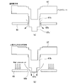
- a vibration electrode film, and a plug part that is a part of the vibration electrode film separated by a slit, and the plug part is supported by a support structure with respect to the back plate, and the implementation of the present invention It is a figure which shows the difference of the effect of Example 1.
- FIG. A vibration electrode film, and a plug part that is a part of the vibration electrode film separated by a slit, and the plug part is supported by a support structure with respect to the back plate, and the implementation of the present invention It is a figure which shows the difference of the effect of Example 1.
- FIG. It is a figure which shows the dimensional relationship of the convex part in Example 1, and a pressure release hole vicinity.
- FIG. 6 is a diagram for explaining a relationship between a convex portion of a back plate and a silicon substrate in Embodiment 1.
- FIG. FIG. 10 is a diagram for explaining the action of the pressure release hole of the vibrating electrode film and the convex portion of the back plate in Example 2. It is a figure for demonstrating the effect
- FIG. 6 is a schematic view of the vicinity of a vibrating electrode film and a back plate of an acoustic sensor in Example 4.
- 10 is a schematic diagram illustrating another example of the vicinity of the vibrating electrode film and the back plate of the acoustic sensor in Example 4.
- FIG. 10 is a schematic diagram illustrating a configuration in the vicinity of a convex portion of a vibrating electrode film and a back plate of an acoustic sensor in Example 5.
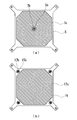
- FIG. 10 is a plan view of the vibration electrode film and the back plate when one set and four sets of pressure release holes and convex portions are provided on the vibration electrode film and the back plate of the acoustic sensor in Example 6. It is a top view of a vibration electrode film and a back plate when eight sets and nine sets of pressure release holes and convex portions are provided on the vibration electrode film and the back plate of the acoustic sensor in Example 6.
- FIG. 10 is a schematic diagram illustrating a configuration in the vicinity of a convex portion of a vibrating electrode film and a back plate of an acoustic sensor in Example 5.
- FIG. 10 is a plan view of the vibration electrode film and the back plate when one set and four sets of pressure release holes and convex portions are provided on the vibration electrode film and the back plate of the acou
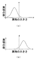
- FIG. 10 is a cross-sectional view showing the vicinity of a set of a convex portion provided on a back plate and a pressure release hole provided on a vibrating electrode film in Example 7. It is the graph which took the size of the foreign material on the horizontal axis, and took the distribution of the number of foreign materials on the vertical axis.
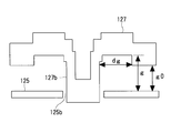
- FIG. 10 is a cross-sectional view illustrating a state around a sound hole and a protrusion provided in a back plate and a pressure release hole provided in a vibration electrode film in Example 8. It is sectional drawing shown about the positional relationship of the sound hole in the backplate of Example 9, a convex part, and the pressure release hole in a vibration electrode film. It is a figure for demonstrating the dimensional relationship of each part of the convex part in a backplate, and the pressure release hole vicinity of a vibration electrode film.
- FIG. 1 is a perspective view showing an example of a conventional acoustic sensor 1 manufactured by MEMS technology.
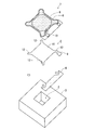
- FIG. 2 is an exploded perspective view showing an example of the internal structure of the acoustic sensor 1.
- the acoustic sensor 1 is a laminated body in which an insulating film 4, a vibrating electrode film (diaphragm) 5, and a back plate 7 are laminated on an upper surface of a silicon substrate (substrate) 3 provided with a back chamber 2.
- the back plate 7 has a structure in which a fixed electrode film 8 is formed on the fixed plate 6, and the fixed electrode film 8 is disposed on the fixed plate 6 on the silicon substrate 3 side.
- the fixed plate 6 of the back plate 7 is provided with a large number of sound holes as perforations (the shaded points of the fixed plate 6 shown in FIGS. 1 and 2 correspond to individual sound holes). .
- a fixed electrode pad 10 for obtaining an output signal is provided at one of the four corners of the fixed electrode film 8.
- the silicon substrate 3 can be formed of, for example, single crystal silicon.
- the vibrating electrode film 5 can be formed of, for example, conductive polycrystalline silicon.
- the vibrating electrode film 5 is a substantially rectangular thin film, and fixed portions 12 are provided at four corners of a vibrating portion 11 having a substantially quadrangular shape that vibrates.
- the vibrating electrode film 5 is disposed on the upper surface of the silicon substrate 3 so as to cover the back chamber 2, and is fixed to the silicon substrate 3 at four fixing portions 12 as anchor portions.
- the vibrating portion 11 of the vibrating electrode film 5 vibrates up and down in response to the sound pressure.
- the vibrating electrode film 5 is not in contact with the silicon substrate 3 or the back plate 7 at a place other than the four fixed portions 12. Therefore, it can vibrate up and down more smoothly in response to the sound pressure.
- a vibrating membrane electrode pad 9 is provided on one of the fixed portions 12 at the four corners of the vibrating portion 11.
- the fixed electrode film 8 provided on the back plate 7 is provided so as to correspond to the vibrating part of the vibrating electrode film 5 excluding the fixed parts 12 at the four corners. This is because the fixed portions 12 at the four corners of the vibrating electrode film 5 do not vibrate in response to the sound pressure, and the capacitance between the vibrating electrode film 5 and the fixed electrode film 8 does not change.
- the sound passes through the sound hole and applies sound pressure to the vibrating electrode film 5. That is, the sound pressure is applied to the vibrating electrode film 5 by the sound holes.
- air in the air gap between the back plate 7 and the vibrating electrode film 5 can easily escape to the outside, thermal noise is reduced, and noise can be reduced.
- the acoustic sensor 1 receives the sound and vibrates the vibrating electrode film 5 due to the structure described above, and the distance between the vibrating electrode film 5 and the fixed electrode film 8 changes.
- the capacitance between the vibrating electrode film 5 and the fixed electrode film 8 changes. Therefore, a DC voltage is applied between the vibrating membrane electrode pad 9 electrically connected to the vibrating electrode membrane 5 and the fixed electrode pad 10 electrically connected to the fixed electrode membrane 8, and the electrostatic By extracting the change in capacitance as an electrical signal, the sound pressure can be detected as an electrical signal.
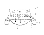
- FIG. 3 is a schematic diagram illustrating a case where an excessive pressure is applied to the acoustic sensor 1.
- the large pressure acts on the vibrating portion 11 of the vibrating electrode film 5 from the sound hole 7 a provided in the back plate 7, and the vibrating portion 11.
- a large distortion may occur, and the vibrating electrode film 5 may be damaged.
- Such an inconvenience may occur when, for example, excessive air pressure acts on the acoustic sensor 1 or when the acoustic sensor 1 falls.
- a countermeasure as shown in FIG. 4 can be considered. That is, as shown in FIG. 4A, by providing the vibrating electrode film 5 with a hole 5a for releasing the applied pressure, the acoustic sensor 1 as shown in FIG.
- the vibration electrode film 5 is provided with the hole 5a that is always open as described above, although the resistance to pressure is improved, sensitivity is lowered particularly in the low frequency range, that is, roll-off is likely to occur, and the acoustic sensor 1 There is a disadvantage that the frequency characteristics of the above deteriorate.
- the vibration electrode film has a plug portion which is a single part separated by dividing the vibration electrode film by a slit, and the plug portion is supported by another structure on the back plate by another structure. Measures to ensure that it is supported at the same height. In this countermeasure, the vibrating electrode film is displaced in response to the pressure difference between the two sides of the film, so that the flow path between the plug portion and the plug portion is expanded to release excessive pressure (for example, Patent Document 2). See).
- the plug portion is configured using a very thin portion of the vibrating electrode film, it is easily damaged.
- the lid-like plug portion is supported with respect to the back plate by using a support structure made of a separate bar-like member, not only the manufacturing process is complicated, but the plug portion is damaged and dropped from the support structure. There is a fear.
- the vibrating electrode film is displaced in response to a pressure difference on both sides of the film, so that the vibrating electrode film and a plug portion which is a single part separated by dividing the vibrating electrode film by a slit.
- the flow path between them is expanded and the excessive pressure is released.
- the vibration electrode film and the plug part which is a part of the vibration electrode film separated by a slit, are used as a flow path between the thin films.
- the vibration electrode film is provided with a hole for releasing the applied pressure, and in a state before the vibration electrode film is deformed, a part of the back plate is used.
- the vibration electrode film is deformed by receiving pressure, the relative movement between the vibrating electrode film and the back plate The penetration of the hole due to the column structure of the back plate is released and the whole hole is exposed, so that the pressure applied to the vibrating electrode film is released.
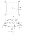
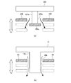
- FIG. 5 shows a schematic view of the vicinity of the vibrating electrode film 15 and the back plate 17 of the acoustic sensor according to this embodiment.
- 5A is a plan view of the vibrating electrode film 15, and
- FIG. 5B is a cross-sectional view of the vibrating electrode film 15, the back plate 17, and the substrate 13 taken along the section BB ′.
- pressure release holes 15 b are provided at the four corners of the vibrating portion 21 of the vibrating electrode film 15.
- the convex portion 17b which is a columnar structure integrally provided on the back plate 17, is pressurized. By passing through the release hole 15b, the pressure release hole 15b is closed.
- the convex portion 17 b is formed as a part of the back plate 17 at the same time when the back plate 17 is formed in the semiconductor manufacturing process.
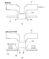
- FIG. 6A shows a state before an excessive pressure is applied to the vibrating electrode film 15.
- FIG. 6B shows a state in which the vibrating electrode film 15 is greatly deformed by an excessive pressure acting on the vibrating electrode film 15.
- the convex portion 17b of the back plate 17 passes through the pressure release hole 15b provided in the vibration electrode film 15 and is closed. In this state, when pressure is applied to the vibrating electrode film 15 from the back plate 17 side, the amount of air passing through the pressure release hole 15b is small and the pressure is not sufficiently released.
- the vibrating electrode film 15 when an excessive pressure is applied to the vibrating electrode film 15, the vibrating electrode film 15 is greatly deformed by the pressure and is deformed away from the back plate 17 as shown in FIG. 6B. If it does so, the convex part 17b will come out from the pressure release hole 15b (penetration will be cancelled
- the convex portion 17b is pressurized. Since the release hole 15b is penetrated and closed, deterioration of the frequency characteristics of the acoustic sensor 10 can be suppressed. Then, when excessive pressure is applied to the vibrating electrode film 15 and the vibrating electrode film 15 is greatly deformed, the projection 17b is released from the pressure release hole 15b (the penetration of the pressure release hole 15b by the projection 17b is released). ), Since the closure is eliminated, the pressure can be sufficiently released from the pressure release hole 15b. As a result, further deformation of the vibrating electrode film 15 can be suppressed, and damage to the vibrating electrode film 15 due to excessive pressure acting on the acoustic sensor 1 can be avoided.
- the above function is realized by using the relative movement of the convex portion 17a provided integrally with the back plate 17 and the pressure release hole 15b provided in the vibration electrode film 15. Therefore, the structure can be simplified and the reliability can be improved.
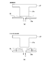
- FIG. 7 and 8 include a vibrating electrode film 105 and a plug part 105a that is a single part of the vibrating electrode film separated by a slit.
- the plug part 105a is attached to the back plate 107.
- FIG. 7A shows the case of the above prior art
- FIG. 7B shows the case of the present embodiment.
- the pressure is released by utilizing the gap between the thin film, namely the vibrating electrode film 105 and the plug portion 105a having the same thickness as the vibrating electrode film 105. Since the presence / absence is adjusted, when a relatively large pressure is applied and the displacement of the vibrating electrode film 105 becomes approximately equal to or greater than the film thickness, the plug portion 105a and the vibrating electrode film are used even if the displacement is within the operating sound pressure range. There is a possibility that the gap between the holes 105 increases rapidly, leading to deterioration of frequency characteristics (sensitivity reduction at low frequencies).
- the gap between the vibrating electrode film 15 and the convex portion 17b is substantially constant, and the frequency characteristics can be stabilized.
- the present embodiment even when the pressure release hole 105b and the vicinity of the vibrating electrode film 105 are warped in the manufacturing process and the flatness is deteriorated, as shown in FIG. As long as the state of penetrating the electrode film 15 is maintained, the gap between the vibrating electrode film 15 and the convex portion 17b is substantially constant, and the frequency characteristics can be stabilized. That is, according to the present embodiment, it is possible to suppress the influence of variations in the manufacturing process on the characteristics of the acoustic sensor 1.
- the overlap in the film thickness direction of the plug portion 105a and the surrounding vibrating electrode film 105 becomes unstable from the initial state, or due to variations in applied voltage, the plug portion 105a and the surrounding vibrating electrode There is no inconvenience that the overlap in the film thickness direction of the film 105 is influenced.
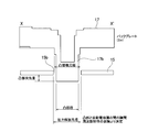
- FIG. 9 shows the dimensional relationship in the vicinity of the convex portion 17b and the pressure release hole 15b in the present embodiment.
- the size of the gap between the convex portion 17b penetrating the pressure release hole 15b can be changed according to the required frequency characteristics.
- it is desirable that the amount of protrusion from the vibrating electrode film 15 at the tip of the convex portion 17 b is 1/2 or more of the film thickness of the vibrating electrode film 15.
- the displacement of the vibration electrode film 15 in the normal use state is often less than or equal to 1 ⁇ 2 of the film thickness.
- the protrusion amount is preferably 0.1 ⁇ m or more and 10 ⁇ m or less.
- the displacement amount of the vibrating electrode film 15 is larger than when the maximum sound pressure in the use volume range is applied. According to this, as long as the acoustic sensor 1 is used in the use volume range, stable frequency characteristics can be obtained. Further, the penetration of the pressure release hole 15b by the convex portion 17b is preferably released when the acting pressure is 200 Pa or more. Then, the acoustic sensor 1 can obtain a stable frequency characteristic for a pressure range of less than 200 Pa.
- the convex portion 17b is removed from the pressure release hole 15b and the closure is eliminated. Excessive deformation of the film 15 can be prevented.
- the vibration electrode film 15 is deformed in a direction approaching the back plate 17, so that the convex portion 17 b does not escape from the pressure release hole 15 b.
- the convex portion 17b has a truncated cone shape in which the diameter is slightly thicker toward the back plate 17 side and the diameter is slightly thinner toward the opposite side of the back plate 17. For this reason, when a pressure is applied to the vibrating electrode film 15 from the back plate 17 side, the gap between the convex portion 17b and the pressure release hole 15b is widened. Thereby, even if the convex portion 17b does not come out of the pressure release hole 15b, the degree of pressure release from the pressure release hole 15b increases as the deformation of the vibrating electrode film 15 increases (the flow rate of air in the pressure release hole 15b increases). And the deformation of the vibrating electrode film 15 is suppressed.
- the gap between the convex portion 17b and the pressure release hole 15b is conversely narrowed.
- the diameter of the portion having the largest cross-sectional area in the convex portion 17b, that is, the root portion is smaller than the diameter of the pressure release hole 15b.
- the vibration electrode film 15 when the vibration electrode film 15 is greatly deformed toward the back plate 17 side, the vibration electrode film 15 is supported by contacting the back plate 17, and further deformation is suppressed. Therefore, in this case, damage to the vibrating electrode film 15 can be avoided even if the convex portion 17b does not come out of the pressure release hole 15b and the closure is not eliminated.
- the shape of the convex portion 17b is not necessarily limited to the truncated cone shape as described above. For example, it may have a cylindrical shape with a substantially constant diameter at any location.
- the pressure of the protrusion 17b and the pressure in the state where the protrusion 17b penetrates the pressure release hole 15b is obtained.
- a gap with the peripheral edge of the release hole 15b functions as a pressure release channel.
- the convex portion 17b is removed from the pressure release hole 15b, and the convex portion 17b and the vibration electrode film 15 in this state
- the gap and the pressure release hole 15b function as a pressure release channel.
- the convex portion 17b corresponds to a convex portion and a convex column structure.
- the silicon substrate 13 does not exist below the convex portion 17b.
- the silicon substrate 13 be disposed so as to avoid a portion facing the convex portion 17b in the acoustic sensor. According to this, the air passing through the pressure release hole 15b can flow more smoothly, and the pressure can be released more reliably by the pressure release hole 15b.
- the tip of the convex portion 17b is located on the same surface as the upper surface (back plate side) of the silicon substrate 13 or on the back plate side. According to this, by forming a film on the silicon substrate 13, it is possible to more reliably form the back plate 17 provided with the convex portions 17b.
- the vibration electrode film 15 and the sacrificial layer that covers the vibration electrode film 15 are formed on the silicon substrate 13, and then the back plate 17 and the protrusion 17 b are formed on the sacrificial layer. It can be realized by a process of forming in the same process and then removing the sacrificial layer. Since the acoustic sensor in this embodiment applies the semiconductor manufacturing technology in this way, it is extremely small, and the positional relationship among the vibrating electrode film 15, the back plate 17, and the convex portion 17b can be formed with high accuracy. .
- the convex portion 17 b is formed by a film forming process different from that of the vibrating electrode film 15 and is formed by the same film forming process as that of the back plate 17. Therefore, the manufacturing process of the back plate 17 and the convex part 17b can be simplified, the integrity of the convex part 17b and the back plate 17 can be further increased, and the reliability can be improved. This manufacturing process is also common in the following examples.
- the convex part 17b may have a hollow pillar structure in a present Example.
- the structure of the convex part 17b is not restricted to a hollow pillar structure.
- the structure of the convex part 17b may be a solid columnar structure.
- the convex portion 17b penetrates the pressure release hole 15b, and the convex portion 17b The case where the tip protrudes from the opposite surface of the vibrating electrode film has been described.
- the convex portion 17b only enters the pressure release hole 15b, and the tip of the convex portion 17b is It does not have to protrude from the opposite surface of the vibrating electrode film.
- the convex portion 17 b is easily removed from the pressure release hole 15 b, and the pressure range in which the frequency characteristics of the acoustic sensor 1 can be satisfactorily maintained becomes small.
- the convex portion 17b penetrates the pressure release hole 15b, and the tip of the convex portion 17b is the surface on the opposite side of the vibrating electrode film. It is possible to obtain an effect comparable to that of protruding from the above.
- the tip of the convex portion 17b may be positioned at the center of the thickness of the vibrating electrode film 15 in a state where excessive pressure is not applied to the vibrating electrode film 15 and the vibrating electrode film 15 is not greatly deformed. .
- the tip of the convex portion 17b can be positioned within the thickness range of the vibrating electrode film 15 within a certain pressure range, and the positional relationship between the convex portion 17b and the pressure release hole 15b is maintained equally. It becomes possible to do.
- Example 2 a second embodiment of the present invention will be described.
- the convex portion 17b is closed by penetrating the pressure release hole 15b of the vibrating electrode film 15, and when excessive pressure acts on the vibrating electrode film 15, the pressure release hole 15b by the convex portion 17b.
- the example where the penetration of the pressure is released and the entire pressure release hole 15b is exposed has been described.
- Example 2 the convex part of the back plate covers the pressure release hole of the vibration electrode film in a normal use state before the vibration electrode film is largely deformed, and excessive pressure is applied to the vibration electrode film.
- An example will be described in which the convex portion is separated from the pressure release hole when acting.
- FIG. 11A shows a state before an excessive pressure is applied to the vibrating electrode film 25.
- FIG. 11B shows a state in which the vibrating electrode film 15 is greatly deformed by an excessive pressure acting on the vibrating electrode film 25.
- the diameter of the convex portion 27 b of the back plate 27 in this embodiment is larger than the diameter of the pressure release hole 25 b provided in the vibration electrode film 25.
- the convex portion 27b of the back plate 27 covers the pressure release hole 25b from the back plate 27 side.
- the vibrating electrode film 25 when an excessive pressure is applied to the vibrating electrode film 25, the vibrating electrode film 25 is greatly deformed by the pressure and is deformed in a direction away from the back plate 27 as shown in FIG. If it does so, the clearance gap between the front-end
- the tip of the convex portion 27b is closed by covering the pressure release hole 25b. Therefore, the deterioration of the frequency characteristics of the acoustic sensor can be suppressed.
- the convex portion 27b is separated from the pressure release hole 25b and the closure is eliminated. Can be prevented from deforming. As a result, it is possible to avoid damage to the vibrating electrode film 25 caused by excessive pressure acting on the acoustic sensor.
- the gap between the tip of the convex portion 27b and the vibrating electrode film 25 and the pressure release hole 25b correspond to a pressure release channel.
- the convex portion 27b corresponds to a convex portion and a convex column structure.
- Example 3 a third embodiment of the present invention will be described.
- the convex portion is provided on the side surface of the back plate, and when an excessive pressure is applied to the vibrating electrode film, the gap between the convex portion and the end surface of the vibrating electrode film is increased. An example of releasing the pressure will be described.
- FIG. 12A is a diagram illustrating the action of the vibration electrode film 35 and the convex portion 37b of the back plate 37 when an excessive pressure is applied to the vibration electrode film 35 in the present embodiment.
- FIG. 12B is a diagram illustrating the action of the vibrating electrode film 45 and the convex portion 47b of the back plate 47 when an excessive pressure is applied to the vibrating electrode film 45 in the present embodiment.
- FIG. 12A is a diagram illustrating the action of the vibration electrode film 35 and the convex portion 37b of the back plate 37 when an excessive pressure is applied to the vibration electrode film 35 in the present embodiment.
- FIG. 12B is a diagram illustrating the action of the vibrating electrode film 45 and the convex portion 47b of the back plate 47 when an excessive pressure is applied to the vibrating electrode film 45 in the present embodiment.
- FIG. 12C is a diagram illustrating the action of the vibrating electrode film 55 and the convex portion 57b of the back plate 57 when an excessive pressure is applied to the vibrating electrode film 55 in the present embodiment.
- the vibrating electrode film indicated by a two-dot chain line shows a state during normal operation where no excessive pressure is applied.
- the vibrating electrode film indicated by the solid line shows a state where an excessive pressure is applied.
- the peripheral portion of the pack plate 37 is bent to form a side surface 37 a, and the tip portion of the side surface 37 a is fixed to the substrate 33.
- the side surface 37a is bent in two steps, and a convex portion 37b is formed by a portion bent outward in the middle of the side surface 37a.
- the end surface of the vibrating electrode film 35 is located above the convex part 37b. . Therefore, the gap between the side surface 37a and the end surface of the vibrating electrode film 35 is narrow. For this reason, the area of the flow path for releasing the pressure is small.
- the peripheral portion of the pack plate 47 is bent to form a side surface 47 a, and the distal end portion of the side surface 47 a is further bent outward to be fixed to the substrate 43.
- tip part of the side surface 47a is bent in the position which protruded from the board
- the end surface of the vibration electrode film 45 is located above the convex part 47b. . Therefore, the gap between the side surface 47a and the end face of the vibrating electrode film 45 is narrow, and the area of the flow path for releasing the pressure is small.
- the peripheral portion of the pack plate 57 is bent to form a side surface 57 a, and the front end portion of the side surface 57 a is fixed to the substrate 53.
- the side surface 57a is bent in the middle, and has a larger taper angle below the bent portion than that above the bent portion, and is connected to the substrate 53 at this larger taper angle.
- the convex part 57b is formed of the bending part from which the taper angle changes in the middle of the side surface 57a.
- the end surface of the vibrating electrode film 55 is positioned above the convex portion 57b as shown by a two-dot chain line in FIG. ing. Therefore, the gap between the side surface 57a and the end face of the vibrating electrode film 55 is narrow, and the area of the flow path for releasing the pressure is small.
- the convex portion is provided on the side surface of the back plate.
- the gap between the convex portion and the end face of the vibrating electrode film is narrow, and the flow area of the pressure release flow path is small. Since it is small, the deterioration of the frequency characteristics of the acoustic sensor can be suppressed.
- the convex portion provided on the side surface of the back plate has been described as being formed by bending the side surface outward, but the method of forming the convex portion is not limited thereto.
- the convex portion may be formed by increasing the thickness of the side surface of the back plate, that is, the horizontal width.
- the convex portions 37b, 47b, and 57b correspond to a convex portion and a convex column structure.
- the back plate has an example in which at least a part of the peripheral portion is bent to form a side surface, fixed to the substrate at the tip of the side surface, and the convex portion is provided on the side surface. did.
- the side surface of the back plate in the present invention is not limited to one formed by bending a part of the back plate.
- the side surface may be formed with the spacer by another member.
- Example 4 a fourth embodiment of the present invention will be described.
- the convex portion 17b is closed by penetrating the pressure release hole 15b of the vibrating electrode film 15, and when excessive pressure acts on the vibrating electrode film 15, the pressure release hole 15b by the convex portion 17b.
- the example in which the penetration of the pressure is released and the entire pressure release hole 15b is exposed has been described.
- Example 4 the convex portion is closed by penetrating the pressure release hole of the vibrating electrode film, and the diameter of the convex portion is smaller on the tip side than on the back plate side.
- the area of the convex portion that passes through the pressure release hole changes, so that the area for closing the pressure release hole changes, and the flow of the pressure release flow path changes.
- FIG. 13 shows a schematic view of the vicinity of the vibrating electrode film 65 and the back plate 67 of the acoustic sensor in this example.
- the vibration electrode film 65 is provided with a pressure release hole 65b.
- the back plate 67 is provided with a convex portion 67b which is a column structure provided integrally in a convex shape. And the diameter of the convex part 67b becomes small discontinuously near the front-end
- the convex portion 67b penetrates the pressure release hole 65b, thereby closing the pressure release hole 65b.
- FIG. 13A shows a state before the vibration electrode film 65 is largely deformed.
- FIG. 13B shows a state in which the vibrating electrode film 55 is greatly deformed by an excessive pressure acting on the vibrating electrode film 65.
- the large diameter portion of the convex portion 67b of the back plate 67 penetrates the pressure release hole 65b provided in the vibration electrode film 65.
- the flow passage area of the flow passage passing through the pressure release hole 65b is small, and the pressure is sufficiently high. Not released.
- the vibrating electrode film 65 is greatly deformed by the pressure and is deformed in a direction away from the back plate 67 as shown in FIG. Then, the large diameter portion of the convex portion 67b comes out of the pressure release hole 65b, and the small diameter convex portion distal end portion 67c passes through the pressure release hole 65b. As a result, the area of the portion of the pressure release hole 65b that is not closed by the convex portion 67b increases. As a result, deformation of the vibrating electrode film 65 is suppressed, and damage to the vibrating electrode film 65 can be avoided.
- the large diameter portion of the convex portion 67b penetrates the pressure release hole 65b. Since it is closed, deterioration of the frequency characteristics of the acoustic sensor can be suppressed. Then, in a state where excessive pressure acts on the vibrating electrode film 65 and the vibrating electrode film 65 is greatly deformed, the small-diameter convex tip end portion 67c of the convex portion 67b penetrates the pressure release hole 65b. Since the flow path area of the air that releases the pressure increases, further deformation of the vibrating electrode film 65 can be suppressed. As a result, it is possible to avoid damage to the vibrating electrode film 65 due to excessive pressure acting on the acoustic sensor.
- FIG. 14 illustrates an example in which the diameter of the convex portion 77b becomes thinner steplessly linearly toward the tip. Even in such a case, when the excessive pressure acts on the vibration electrode film 75 and the vibration electrode film 75 is greatly deformed, the small diameter portion on the tip side of the convex portion 77b penetrates the pressure release hole 75b. Since the flow area of the air that releases the pressure is increased, excessive deformation of the vibrating electrode film 75 can be prevented.
- the gap between the protrusions 67b and 77b or the protrusion tip 67c and the peripheral edge of the pressure release holes 65b and 75b corresponds to the pressure release flow path.
- the convex portions 67b and 77b and the convex tip end portion 67c correspond to a convex portion and a convex column structure.
- the channel area means the cross-sectional area of the channel that affects the flow rate of air passing through the channel.
- the convex portion of the back plate may be formed at any position of the back plate. However, it is desirable to be provided in a region outside the fixed electrode film provided on the back plate.
- the convex portion is not disposed in the peripheral portion of the back plate, but is provided in a position corresponding to the central portion of the vibration electrode film in the back plate, and the pressure release hole is provided in the central portion of the vibration electrode film. You may do it. According to this, since the pressure can be released at the place where the displacement amount of the vibrating electrode film is the largest, the sensitivity of the pressure release can be improved. Moreover, the cross-sectional shape of a convex part and a pressure release hole does not need to be circular, and an ellipse or a polygon may be sufficient. Moreover, the number of convex parts and pressure release holes is not particularly limited. One set may be used, or a plurality of sets, for example, five or more sets may be used.
- the acoustic sensor to which the present invention is applied is not limited to this aspect.
- the present invention may be applied to an acoustic sensor having a configuration in which the arrangement of the back plate and the vibrating electrode film is interchanged.
- FIG. 15 shows a schematic view of the vibrating electrode film 85 and the back plate 87 of the acoustic sensor according to the present embodiment, particularly in the vicinity of the convex portion 87b.
- the convex portion 87b in this embodiment has a smaller ratio of height to diameter than the convex portion 77b shown in FIG.
- the outer shape of this has a substantially truncated cone shape having a tapered side surface whose diameter decreases toward the tip side.
- the size of the step from the back plate 87 of the convex portion 87b can be suppressed, and the inclination angle on the tapered side surface can be relaxed. Thereby, it is possible to suppress the stress concentration at the step and relatively increase the strength of the convex portion 87b. Further, when the convex portion 87b is formed by film formation by a semiconductor manufacturing process, the film quality itself on the side surface can be improved. In this sense, the strength of the convex portion 87b can be increased.
- the slope angle of the side surface of the convex portion 87b is desirably 60 degrees or greater and 85 degrees or less with respect to the back plate surface.
- the diameter of the pressure release hole 85b formed in the vibrating electrode film 85 is increased to several ⁇ m or more, it is found that the state of the convex portion 87b is stabilized by making the side surface of the convex portion 87b into a tapered surface. Yes.
- the gap between the convex portion 87b and the end surface of the pressure release hole 85b is increased. Since it spreads, foreign matter mixed between the vibrating electrode film 85 and the back plate 87 is removed from the gap, and there is an advantage that foreign matter is not easily deposited or pinched near the convex portion 87b.
- the diameter of the convex part 87b can be selected according to a specification in the range of 2 micrometers or more and 100 micrometers or less.
- FIG. 15 shows, as an example, a state where the ratio of the protruding amount of the convex portion 87b from the back plate 87 and the diameter of the tip of the convex portion 87b is set to about 6: 1.
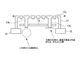
- FIG. 16A shows the vibration electrode film 5 in the case where one set of the pressure release hole 5b and the convex portion 7b is provided on the vibration electrode film 5 and the back plate of the acoustic sensor as shown in FIG. And the top view of the fixed electrode film
- the set of the pressure release hole 5b and the convex portion 7b is formed at the center of the vibrating electrode film 5 and the fixed electrode film 7c.
- the merits of this configuration are as follows: (1) Since there is only one set of the pressure release hole 5b and the convex portion 7b that affects the frequency characteristic, there is little variation in the frequency characteristic as an acoustic sensor.
- the vibration electrode film is often fixed at the ends (four corners in the case of a rectangular shape). Therefore, in this configuration, the pressure release hole and the convex part are formed regardless of the shape of the vibration electrode film.
- the vibration electrode film can be formed in a portion with a large amount of displacement, and the pressure release function can be exhibited with higher sensitivity or reliability.
- FIG. 16B shows the vibration when four sets of pressure release holes 15b and convex portions 17b are provided on the vibration electrode film 15 and the back plate of the acoustic sensor as shown in FIG.
- the top view of the electrode film 15 and the fixed electrode film 17c of a backplate is shown.
- the set of the pressure release hole 15 b and the convex portion 17 b is formed near the fixed portions at the four corners of the vibrating electrode film 15.
- Advantages of this configuration are as follows: (1) Since the set of the pressure release hole 15b and the convex portion 17b is arranged outside the fixed electrode film 17c of the back plate, the area of the fixed electrode film 17c of the back plate is reduced.
- FIG. 17A when the vibration electrode film 95 and the back plate of the acoustic sensor are provided with eight sets of pressure release holes 95b and convex portions 97b, the vibration electrode film 95 and the back plate are fixed.
- the top view of the electrode film 97c is shown.
- the set of the pressure release hole 95b and the convex portion 97b is formed in the vicinity of the fixed portion at the four corners of the vibration electrode film 95 and at the central portion of the four sides.
- the merit of this configuration is that (1) all the convex portions 97b are removed from the pressure release holes 95b as compared with the case of FIG. 16B in which four sets of the pressure release holes 15b and the convex portions 17b are provided.
- FIG. 17B illustrates the vibration electrode film 115 and the back plate fixed electrode film 117c when nine sets of the pressure release holes 115b and the convex portions 117b are provided on the vibration electrode film 115 and the back plate of the acoustic sensor.
- the top view of is shown.
- the set of the pressure release hole 115b and the convex portion 117b is formed in the central portion of the vibrating electrode film 115, in the vicinity of the fixed portion at the four corners, and in the central portion of the four sides.
- the arrangement of the pressure release hole and the convex portion is symmetrical with respect to the central portion of the back plate. There is an effect that the behavior is stabilized.
- eight sets of pressure release holes 95b and convex portions 97b shown in FIG. 17 are provided, or when nine sets of pressure release holes 115b and convex portions 117b are provided, eight-fold symmetry (45 Since the arrangement of the pressure release holes and projections is equivalent in any direction, the displacement of the vibrating membrane is made uniform and uniform when subjected to sound waves or external pressure. Contributes to improvement and sensitivity improvement.
- the air around each pressure release hole moves in translation toward the pressure release hole and then escapes from the pressure release hole to the opposite side of the vibrating electrode film. Therefore, in this embodiment, if the pressure release holes and the protrusions are arranged as far as possible from each other, it is possible to release a larger amount of air from the pressure release holes in total, and the pressure can be increased more efficiently. Can be released. On the other hand, if the pressure release hole and the pair of projections are close to each other, only air in a region close to the pressure release hole can escape, so the amount of air that can be released is limited and the pressure release efficiency is reduced. .
- the arrangement of the pressure release hole and the convex portion in the present embodiment is an example in which they are arranged most apart from each other in the number of sets.
- Example 7 Next, a seventh embodiment of the present invention will be described.
- an example will be described in which a gap in the thickness direction between the back plate and the vibrating electrode film is increased around the convex portion of the back plate to prevent foreign matter.
- FIG. 18 is a cross-sectional view showing the vicinity of a set of a convex portion 127b provided on the back plate 127 and a pressure release hole 125b provided on the vibrating electrode film 125 in the present embodiment.
- the gap between the back plate 127 and the vibrating electrode film 125 is set to g0 in a region far from the convex portion 127b, and is set to g (> g0) in a region near the convex portion 127b. .
- the back plate 127 and the vibrating electrode film can be obtained even when foreign matter is accumulated or pinched in the vicinity of the convex portion 127b of the back plate 127 and the pressure release hole 125b of the vibrating electrode film 125.
- the amount of change in the gap of 125 can be reduced, and the influence on the frequency characteristics of the acoustic sensor can be reduced.
- FIG. 19 is a graph in which the horizontal axis represents the size (diameter) of foreign matter and the vertical axis represents the number of foreign matters.
- FIG. 19A shows the case where the majority of the size distribution of the foreign matter is smaller than the size g of the gap between the back plate 127 and the vibrating electrode film 125 in the region close to the convex portion 127b.
- the majority of the distribution of the size of the foreign matter is larger than the size g of the gap between the back plate 127 and the vibrating electrode film 125 in the region close to the convex portion 127b.
- the range in which the gap between the back plate 127 and the vibrating electrode film 125 is increased is preferably as small as possible in consideration of the sensitivity as an acoustic sensor.
- the distance dg from the side surface of the convex portion 127b may be in the range of 0 ⁇ dg ⁇ g. Alternatively, a wider range may be used.
- Example 8 Next, an eighth embodiment of the present invention will be described. In the present embodiment, an example will be described in which foreign matter countermeasures are performed by reducing the area ratio of the sound holes around the convex portion of the back plate.
- the foreign matter countermeasure is taken by reducing the area ratio of the sound holes in the vicinity of the convex portion of the back plate.
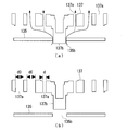
- FIG. 20 is a cross-sectional view showing a state around the sound hole 137a and the convex portion 137b provided in the back plate 137 and the pressure release hole 135b provided in the vibration electrode film 135 in this embodiment.
- FIG. 20A shows a state where the convex portion 137b has not come out of the pressure release hole 135b
- FIG. 20B shows a state where the convex portion 137b becomes a pressure release hole 135b when a large pressure is applied. It shows a state where it has left.
- the diameter of the sound hole 137a in the back plate 137 is set to d0 in the region far from the convex portion 137b, and in the region close to the convex portion 137b, d. ( ⁇ D0).
- the acoustic resistance (air passage resistance) that determines the frequency characteristics of the acoustic sensor is such that the side surface of the convex portion 137b in the back plate 137 and the vibration electrode film 135 This is the total value of the acoustic resistance in the gap between the pressure release hole 135b and the acoustic resistance in the sound hole 137a. Therefore, when the diameter of the sound hole 135a is reduced in the vicinity of the convex portion 137b as in the present embodiment, the total acoustic resistance in this region is increased.
- the diameter of the sound hole 137a is smaller in the region close to the convex portion 137b than in the region far from the convex portion 137b, thereby reducing the area ratio of the sound hole.
- the area ratio of the sound holes is increased. It may be lowered.
- the range in which the area ratio of the sound hole 137a is reduced may be, for example, a range in which the distance from the side surface of the convex portion 137b is within twice the diameter of the convex portion 137b. Good. Alternatively, a wider range may be used.
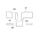
- FIG. 21 is a cross-sectional view of the positional relationship between the sound hole 147a and the convex portion 147b in the back plate 147 and the pressure release hole 145b in the vibration electrode film 145 of the present embodiment. *
- the horizontal position of the sound hole 147a and the pressure release hole 145b in the back plate 147 overlap.
- the sound hole 145a is open at a part immediately above the gap between the convex portion 147b and the pressure release hole 145b. According to this, a space penetrating both the vibrating electrode film 145 and the back plate 147 can be formed, and foreign matter can easily pass through this space.
- the convex portion 147b on the back plate 147, the vibrating electrode It is possible to reduce the probability that foreign matter accumulates or gets caught in the vicinity of the pressure release hole 145b of the film 145.
- the formation of a space that penetrates both the vibrating electrode film 145 and the back plate 147 is expected to increase the attenuation of sensitivity in the low frequency region of the acoustic sensor, and It is expected that the pressure release function is improved when the pressure is applied and the convex portion 147b comes out of the pressure release hole 145b. Therefore, in this embodiment, in addition to being able to strengthen countermeasures against foreign matter, it is possible to improve pressure resistance while attenuating the sensitivity of the acoustic sensor in the low frequency region at a constant level.
- FIG. 22 is a diagram for explaining the dimensional relationship between the protrusions 17 b in the back plate 17 and the respective portions in the vicinity of the pressure release holes 15 b of the vibration electrode film 15.
- a distance x3 between the silicon substrate edge 12a that overlaps the back plate 17 and the vibration electrode film 15 in plan view and the convex portion 17b is as follows: (1) silicon substrate edge The tolerance for variation in the distance x3 between 12a and the convex portion 17b increases. (2) The displacement of the vibrating electrode film 15 is not easily inhibited by the silicon substrate edge 12a. There is a merit such as. On the other hand, there are no direct disadvantages. If this distance is larger than 0 ⁇ m, the vibration electrode film 15 can be displaced at least by the height y2 of the pressure release hole 15b. Therefore, an effective pressure release function can be obtained depending on the design. For example, the distance x3 may be 3 ⁇ m or more, which is a manufacturing variation in the position of the silicon substrate edge 12a.
Landscapes
- Engineering & Computer Science (AREA)
- Physics & Mathematics (AREA)
- Acoustics & Sound (AREA)
- Signal Processing (AREA)
- Microelectronics & Electronic Packaging (AREA)
- Computer Hardware Design (AREA)
- Manufacturing & Machinery (AREA)
- Toxicology (AREA)
- General Health & Medical Sciences (AREA)
- Health & Medical Sciences (AREA)
- Multimedia (AREA)
- Electrostatic, Electromagnetic, Magneto- Strictive, And Variable-Resistance Transducers (AREA)
- Pressure Sensors (AREA)
- Micromachines (AREA)
Abstract
Description
前記基板の開口に対向するように配設されたバックプレートと、
前記バックプレートとの間に空隙を介して該バックプレートに対向するように配設された振動電極膜と、
を備え、
前記振動電極膜の変位を該振動電極膜と前記バックプレートの間の静電容量の変化に変換する静電容量型トランスデューサにおいて、
前記振動電極膜の一部と前記バックプレートに一体に設けられた凸状の部分との隙間により形成される空気の流路であって、前記振動電極膜が圧力を受けて変形した際に、該振動電極膜と前記バックプレートに一体に設けられた凸状の部分との相対移動によって流路面積が増大することで、前記振動電極膜に印加された圧力を解放する圧力解放流路を、さらに備えることを特徴とする。
前記圧力解放流路は、前記振動電極膜の端面と、前記バックプレートの側面に一体に形成された凸状の部分との隙間により形成され、
前記振動電極膜が圧力を受けて変形した際に、該振動電極膜の端面と前記バックプレートの側面に形成された凸状の部分とが相対移動してずれることにより、前記振動電極膜の端面と、前記バックプレートの側面との隙間が増大することで、前記振動電極膜に印加された圧力を解放するようにしてもよい。
少なくとも前記凸状の柱構造の先端部は前記孔の径より小さい径を有するとともに、前記振動電極膜が圧力を受けて変形する前の状態においては、前記凸状の柱構造が前記孔に侵入し、
前記振動電極膜が圧力を受けて変形した際に、該振動電極膜と前記バックプレートの凸状の柱構造とが相対移動し、前記凸状の柱構造による前記孔への侵入を解除することで、前記振動電極膜に印加された圧力を解放するようにしてもよい。
前記凸状の柱構造は前記孔の径より大きい径を有するとともに、前記振動電極膜が圧力を受けて変形する前の状態においては、前記凸状の柱構造の先端が前記孔を前記バックプレート側から覆い、
前記振動電極膜が圧力を受けて変形した際に、該振動電極膜と前記バックプレートの凸状の柱構造とが相対移動し、前記凸状の柱構造の先端が前記孔から離れることで、前記振動電極膜に印加された圧力を解放するようにしてもよい。
以下、本願発明の実施形態について図を参照しながら説明する。以下に示す実施形態は、本願発明の一態様であり、本願発明の技術的範囲を限定するものではない。なお、本発明は、静電トランスデューサ全体に適用することが可能であるが、以下においては、静電トランスデューサを音響センサとして用いる場合について説明する。しかしながら、本発明に係る音声トランスデューサは、振動電極膜の変位を検出するものであれば、音響センサ以外のセンサとしても利用できる。例えば、圧力センサの他、加速度センサや慣性センサ等として使用しても構わない。また、センサ以外の素子、例えば、電気信号を変位に変換するスピーカ等として使用しても構わない。
次に、本発明における実施例2について説明する。実施例1においては、凸部17bが、振動電極膜15の圧力解放孔15bを貫通することで閉鎖し、過大な圧力が振動電極膜15に作用した場合に、凸部17bによる圧力解放孔15bの貫通が解除されて圧力解放孔15bの全体が露出される例について説明した。
次に、本発明における実施例3について説明する。実施例3においては、凸部がバックプレートの側面に設けられており、振動電極膜に過大な圧力が作用した場合に、凸部と振動電極膜の端面との間の隙間が大きくなることで、圧力を解放する例について説明する。
次に、本発明における実施例4について説明する。実施例1においては、凸部17bが、振動電極膜15の圧力解放孔15bを貫通することで閉鎖し、過大な圧力が振動電極膜15に作用した場合に、凸部17bによる圧力解放孔15bの貫通が解かれて圧力解放孔15bの全体が露出される例について説明した。
次に、本発明の実施例5について説明する。本実施例においては、凸部が特に底浅で底面が平坦な鍋状の構造を有する例について、説明する。
次に、本発明の実施例6について説明する。本実施例においては、振動電極膜に設けられた圧力解放孔と、バックプレートに設けられた凸部の組の数のバリエーションと、その特性について説明する。
次に、本発明の実施例7について説明する。本実施例においては、バックプレートにおける凸部の周囲で、バックプレートと振動電極膜の厚み方向のギャップを大きくすることで異物対策とする例について説明する。
次に、本発明の実施例8について説明する。本実施例においては、バックプレートにおける凸部の周囲で、音孔の面積比率を低下させることで異物対策とする例について説明する。
次に、本発明の実施例9について説明する。本実施例においては、バックプレートにおける凸部の周囲の音孔と、振動電極膜の圧力解放孔とが、平面視において重なる構成とすることで異物対策とする例について説明する。
次に、上記の実施例における各部の寸法の望ましい状態について考察する。図22は、バックプレート17における凸部17b、振動電極膜15の圧力解放孔15bの近傍の各部の寸法関係を説明するための図である。
図22において、一般的には、凸部17bの先端の振動電極膜15からの突出量y1が大きくなると、(1)大きい音圧が加わった際にも、凸部17bが圧力解放孔15bから抜けづらく、FR、THD異常になり難くなる。(2)凸部17bの長さ方向に対する、各部材の配置バラツキの許容度が大きくなる。といったメリットがある。一方、(1)比較的高い圧力が作用しないと凸部17bが圧力解放孔15bから抜けず、バラツキによっては、必要な圧力範囲において圧力解放の機能が働かなくなるリスクがある。(2)凸部17bの周辺における、バックプレート17と振動電極膜15の間に異物が堆積した場合に、振動電極膜15の変形が大きくなり、音響センサの周波数特性への異物の影響が大きくなる。といったデメリットがある。
図22において、バックプレート17の凸部17bと振動電極膜15の圧力解放孔15bとのクリアランスx1が狭い場合には、(1)周波数特性における低周波領域の減衰が緩やかになり、より良い周波数特性が得られる。というメリットがある。一方、(1)凸部17bと圧力解放孔15bとが接触するリスクが増大する。(2)凸部17bと圧力解放孔15bとの隙間についての寸法バラツキの許容度が小さくなる。というデメリットがある。これらの点を鑑み、上記の実施例において凸部17bと圧力解放孔15bの間の隙間は、0.2μm以上20μm以下が適切な値である。
図22において、バックプレート17の凸部17bと、固定電極膜17cとの間の距離x2については、この距離x2が小さいと(1)凸部17bを設けることによる固定電極膜17cの電極面積のロスを小さく抑えることができ、感度低下を抑制できる。というメリットがある。一方、(1)凸部17bの近傍に導電性の異物が堆積したり挟まった場合に、ショートする危険性が高くなるというデメリットがある。これらの点を鑑み、バックプレート17における凸部17bと、固定電極膜17cとの間の距離は、1μm以上15μm以下とすることが適切である。
図22において、バックプレート17及び振動電極膜15と平面視でオーバーラップしているシリコン基板エッジ12aと、凸部17bの間の距離x3は、この距離x3が大きいと、(1)シリコン基板エッジ12aと凸部17bの間の距離x3のバラツキに対する許容度が大きくなる。(2)振動電極膜15の変位がシリコン基板エッジ12aによって阻害されづらい。といったメリットがある。一方、直接的なデメリットは特にないと言える。この距離は、0μmより大きければ、最低でも圧力解放孔15bの高さy2分は振動電極膜15が変位可能であるので、設計次第では有効な圧力解放機能を有する構成にすることができる。例えば、上記の距離x3は、シリコン基板エッジ12aの位置の製造ばらつきである3μm以上としてもよい。
2・・・バックチャンバー
3、13・・・(シリコン)基板
5、15、25、35、45、55、65、75、85、95、115、125、135、145・・・振動電極膜
7、17、27、37,47,57、67、77、87、127,137、147・・・バックプレート
7c、17c、97c、117c・・・固定電極膜
15b、25b、65b、75b、85b、95b、115b、125b、135b、145b・・・圧力解放孔
17b、27b、37b、47b、57b、67b、77b、87b、97b、117b、127b、137b、147b・・・凸部
Claims (24)
- 表面に開口を有する基板と、
前記基板の開口に対向するように配設されたバックプレートと、
前記バックプレートとの間に空隙を介して該バックプレートに対向するように配設された振動電極膜と、
を備え、
前記振動電極膜の変位を該振動電極膜と前記バックプレートの間の静電容量の変化に変換する静電容量型トランスデューサにおいて、
前記振動電極膜の一部と前記バックプレートに一体に設けられた凸状の部分との隙間により形成される空気の流路であって、前記振動電極膜が圧力を受けて変形した際に、該振動電極膜と前記バックプレートに一体に設けられた凸状の部分との相対移動によって流路面積が増大することで、前記振動電極膜に印加された圧力を解放する圧力解放流路を、さらに備えることを特徴とする静電容量型トランスデューサ。 - 前記バックプレートは、周辺部の少なくとも一部が屈曲して側面を形成するとともに該側面の先端部において前記基板に固定され
前記圧力解放流路は、前記振動電極膜の端面と、前記バックプレートの側面に一体に形成された凸状の部分との隙間により形成され、
前記振動電極膜が圧力を受けて変形した際に、該振動電極膜の端面と前記バックプレートの側面に形成された凸状の部分とが相対移動してずれることにより、前記振動電極膜の端面と、前記バックプレートの側面との隙間が増大することで、前記振動電極膜に印加された圧力を解放することを特徴とする請求項1に記載の静電容量型トランスデューサ。 - 前記凸状の部分は、凸状の柱構造であり、
前記圧力解放流路は、前記振動電極膜に設けられた孔と、前記バックプレートから前記振動電極膜側に一体に設けられた凸状の柱構造との隙間により形成され、
少なくとも前記凸状の柱構造の先端部は前記孔の径より小さい径を有するとともに、前記振動電極膜が圧力を受けて変形する前の状態においては、前記凸状の柱構造が前記孔に侵入し、
前記振動電極膜が圧力を受けて変形した際に、該振動電極膜と前記バックプレートの凸状の柱構造とが相対移動し、前記凸状の柱構造による前記孔への侵入を解除することで、前記振動電極膜に印加された圧力を解放することを特徴とする請求項1に記載の静電容量型トランスデューサ。 - 前記凸状の部分は、凸状の柱構造であり、
前記圧力解放流路は、前記振動電極膜に設けられた孔と、前記バックプレートから前記振動電極膜側に一体に設けられた凸状の柱構造との隙間により形成され、
前記凸状の柱構造は前記孔の径より大きい径を有するとともに、前記振動電極膜が圧力を受けて変形する前の状態においては、前記凸状の柱構造の先端が前記孔を前記バックプレート側から覆い、
前記振動電極膜が圧力を受けて変形した際に、該振動電極膜と前記バックプレートの凸状の柱構造とが相対移動し、前記凸状の柱構造の先端が前記孔から離れることで、前記振動電極膜に印加された圧力を解放することを特徴とする請求項1に記載の静電容量型トランスデューサ。 - 前記振動電極膜が圧力を受けて変形する前の状態においては、前記凸状の柱構造が前記孔を貫通し、該凸状の柱構造の先端は、前記振動電極膜に対して前記バックプレートの反対側に位置することを特徴とする請求項3に記載の静電容量型トランスデューサ。
- 前記凸状の柱構造の径は、該凸状の柱構造の先端から前記バックプレートに向かうにつれて大きくなり、または一定であることを特徴とする請求項3または5に記載の静電容量型トランスデューサ。
- 前記凸状の柱構造は、前記バックプレートと同一の成膜工程によって形成されたものであることを特徴とする請求項3から6のいずれか一項に記載の静電容量型トランスデューサ。
- 前記振動電極膜は、前記基板にアンカー部において固定されるとともに、該アンカー部以外の場所においては、前記基板及び前記バックプレートに接触しないことを特徴とする請求項1から7のいずれか一項に記載の静電容量型トランスデューサ。
- 前記バックプレートは、複数の穿孔を有することを特徴とする請求項1から8のいずれか一項に記載の静電容量型トランスデューサ。
- 前記基板は、前記バックプレートに一体に設けられた凸状の柱構造に対向する部分を避けて配置されることを特徴とする請求項3に記載の静電容量型トランスデューサ。
- 前記バックプレートは前記基板に対向して配置され、
前記凸状の柱構造は、前記バックプレートから前記基板側に向けて設けられるとともに、その先端が、前記基板の前記バックプレート側の表面と同面または、該表面よりバックプレート側に位置することを特徴とする請求項3に記載の静電容量型トランスデューサ。 - 前記バックプレートは中央部に固定電極膜を有し、
前記凸状の部分は、前記バックプレートにおける前記固定電極膜の外側に設けられたことを特徴とする請求項1および請求項3から11のうちいずれか一項に記載の静電容量型トランスデューサ。 - 前記凸状の部分は、前記バックプレートにおける中央部に設けられたことを特徴とする請求項1および請求項3から11のうちいずれか一項に記載の静電容量型トランスデューサ。
- 前記凸状の柱構造における側面はテーパ面を形成し、該テーパ面の前記バックプレートに対する傾斜角は、60度以上85度以下であることを特徴とする請求項6に記載の音響トランスデューサ。
- 前記振動電極膜は、略長方形型の形状を有するとともに4隅に設けられた固定部において固定され、
前記凸状の部分は、前記バックプレートにおいて、平面視で前記振動電極膜の4隅であって前記固定部よりも内側に相当する部分に4箇所設けられたことを特徴とする請求項3または4に記載の静電容量型トランスデューサ。 - 前記凸状の部分は、前記バックプレートにおける中央部に1箇所設けられたことを特徴とする請求項13に記載の静電容量型トランスデューサ。
- 前記凸状の部分は、前記バックプレートにおいて、さらに、平面視で前記振動電極膜の4辺の中央部に相当する部分に4箇所設けられ、合計8箇所設けられたことを特徴とする請求項15に記載の静電容量型トランスデューサ。
- 前記凸状の部分は、前記バックプレートの中央部にさらに1箇所設けられ、合計9箇所設けられたことを特徴とする請求項17に記載の静電容量型トランスデューサ。
- 前記振動電極膜が圧力を受けて変形する前に、前記凸状の柱構造が前記孔に侵入した状態において、前記凸条の柱構造と前記孔との間の隙間は、片側0.2μm以上20μm以下であることを特徴とする、請求項3に記載の静電容量型トランスデューサ。
- 前記バックプレートは、平面視において前記凸状の部分が設けられた場所を避けて前記固定電極膜を有し、前記凸条の部分と前記固定電極膜との距離を1μm以上15μm以下としたことを特徴とする請求項3または4に記載の静電容量型トランスデューサ。
- 前記バックプレートと前記振動電極膜との間の隙間の大きさは、前記凸状の部分の周囲の所定範囲内については、該所定範囲外よりも大きくされたことを特徴とする請求項3または4に記載の静電容量型トランスデューサ。
- 前記バックプレートにおける音孔の大きさは、前記凸状の部分の周囲の所定範囲内については、該所定範囲外よりも小さくされたことを特徴とする請求項3または4に記載の静電容量型トランスデューサ。
- 前記バックプレートにおける前記凸状の部分の周囲の所定範囲内における音孔と、前記振動電極膜に設けられた孔とは、平面視において、少なくとも一部が重なるように配置されたことを特徴とする請求項3に記載の静電容量型トランスデューサ。
- 請求項1から23のいずれか一項に記載の静電容量型トランスデューサを有し、音圧を前記振動電極膜と前記バックプレートの間の静電容量の変化に変換して検出する音響センサ。
Priority Applications (5)
| Application Number | Priority Date | Filing Date | Title |
|---|---|---|---|
| JP2017505405A JP6332549B2 (ja) | 2015-03-12 | 2016-03-10 | 静電容量型トランスデューサ及び音響センサ |
| KR1020177005904A KR101884143B1 (ko) | 2015-03-12 | 2016-03-10 | 정전용량형 트랜스듀서 및 음향 센서 |
| CN201680002574.XA CN106688246B (zh) | 2015-03-12 | 2016-03-10 | 静电电容式转换器及音响传感器 |
| US15/509,221 US10375482B2 (en) | 2015-03-12 | 2016-03-10 | Capacitance type transducer and acoustic sensor |
| DE112016000099.5T DE112016000099T5 (de) | 2015-03-12 | 2016-03-10 | Kapazitiver Messumformer und akustischer Sensor |
Applications Claiming Priority (2)
| Application Number | Priority Date | Filing Date | Title |
|---|---|---|---|
| JP2015-050100 | 2015-03-12 | ||
| JP2015050100 | 2015-03-12 |
Publications (1)
| Publication Number | Publication Date |
|---|---|
| WO2016143867A1 true WO2016143867A1 (ja) | 2016-09-15 |
Family
ID=56879556
Family Applications (1)
| Application Number | Title | Priority Date | Filing Date |
|---|---|---|---|
| PCT/JP2016/057630 Ceased WO2016143867A1 (ja) | 2015-03-12 | 2016-03-10 | 静電容量型トランスデューサ及び音響センサ |
Country Status (6)
| Country | Link |
|---|---|
| US (1) | US10375482B2 (ja) |
| JP (1) | JP6332549B2 (ja) |
| KR (1) | KR101884143B1 (ja) |
| CN (1) | CN106688246B (ja) |
| DE (1) | DE112016000099T5 (ja) |
| WO (1) | WO2016143867A1 (ja) |
Cited By (2)
| Publication number | Priority date | Publication date | Assignee | Title |
|---|---|---|---|---|
| JP2018098615A (ja) * | 2016-12-12 | 2018-06-21 | オムロン株式会社 | 音響センサ及び静電容量型トランスデューサ |
| JP2018098526A (ja) * | 2016-12-08 | 2018-06-21 | オムロン株式会社 | 静電容量型トランスデューサシステム、静電容量型トランスデューサ及び、音響センサ |
Families Citing this family (12)
| Publication number | Priority date | Publication date | Assignee | Title |
|---|---|---|---|---|
| JP6658126B2 (ja) * | 2016-03-10 | 2020-03-04 | オムロン株式会社 | 静電容量型トランスデューサ及び音響センサ |
| JP6986365B2 (ja) * | 2016-08-23 | 2021-12-22 | アルパイン株式会社 | 車載用スピーカシステム |
| CN106375912B (zh) * | 2016-08-31 | 2020-03-17 | 歌尔股份有限公司 | 一种mems麦克风中的振膜及mems麦克风 |
| CN206533541U (zh) * | 2017-01-25 | 2017-09-29 | 歌尔股份有限公司 | 一种mems麦克风 |
| CN107509150B (zh) * | 2017-09-29 | 2020-06-09 | 瑞声声学科技(深圳)有限公司 | Mems麦克风 |
| US12253391B2 (en) | 2018-05-24 | 2025-03-18 | The Research Foundation For The State University Of New York | Multielectrode capacitive sensor without pull-in risk |
| WO2020033534A1 (en) * | 2018-08-08 | 2020-02-13 | Graphaudio | High volume manufacturing of micro electrostatic transducers |
| FR3088721B1 (fr) * | 2018-11-21 | 2022-10-07 | Univ Montpellier | Capteur capacitif pour la spectroscopie photo-acoustique, dispositif et procédé mettant en œuvre un tel capteur. |
| TWI770543B (zh) * | 2020-06-29 | 2022-07-11 | 美律實業股份有限公司 | 麥克風結構 |
| CN116491129B (zh) * | 2021-04-23 | 2026-07-03 | 深圳市韶音科技有限公司 | 传感装置 |
| WO2024207210A1 (zh) * | 2023-04-04 | 2024-10-10 | 瑞声声学科技(深圳)有限公司 | Mems麦克风 |
| CN116982759A (zh) * | 2023-09-26 | 2023-11-03 | 苏州敏芯微电子技术股份有限公司 | 气流传感器及气流传感器封装结构 |
Citations (3)
| Publication number | Priority date | Publication date | Assignee | Title |
|---|---|---|---|---|
| WO2010004766A1 (ja) * | 2008-07-11 | 2010-01-14 | ローム株式会社 | Memsデバイス |
| JP2014057175A (ja) * | 2012-09-11 | 2014-03-27 | Omron Corp | 音響トランスデューサ |
| US8692340B1 (en) * | 2013-03-13 | 2014-04-08 | Invensense, Inc. | MEMS acoustic sensor with integrated back cavity |
Family Cites Families (13)
| Publication number | Priority date | Publication date | Assignee | Title |
|---|---|---|---|---|
| DE102006001493B4 (de) | 2006-01-11 | 2007-10-18 | Austriamicrosystems Ag | MEMS-Sensor und Verfahren zur Herstellung |
| CN101584226B (zh) | 2007-01-17 | 2013-08-21 | 美国亚德诺半导体公司 | 带有压力释放的麦克风 |
| JP2008199226A (ja) * | 2007-02-09 | 2008-08-28 | Yamaha Corp | コンデンサマイク装置 |
| US20080192963A1 (en) | 2007-02-09 | 2008-08-14 | Yamaha Corporation | Condenser microphone |
| US20090060232A1 (en) * | 2007-08-08 | 2009-03-05 | Yamaha Corporation | Condenser microphone |
| US20090175477A1 (en) | 2007-08-20 | 2009-07-09 | Yamaha Corporation | Vibration transducer |
| JP2009071862A (ja) * | 2008-11-17 | 2009-04-02 | Yamaha Corp | コンデンサマイクロホン |
| JP5400708B2 (ja) | 2010-05-27 | 2014-01-29 | オムロン株式会社 | 音響センサ、音響トランスデューサ、該音響トランスデューサを利用したマイクロフォン、および音響トランスデューサの製造方法 |
| CN103347808B (zh) | 2011-12-29 | 2016-02-10 | 歌尔声学股份有限公司 | 硅基mems麦克风、包含该麦克风的系统和封装 |
| GB2506174A (en) | 2012-09-24 | 2014-03-26 | Wolfson Microelectronics Plc | Protecting a MEMS device from excess pressure and shock |
| JP6127600B2 (ja) * | 2013-03-12 | 2017-05-17 | オムロン株式会社 | 静電容量型センサ、音響センサ及びマイクロフォン |
| CN104053104A (zh) * | 2013-03-12 | 2014-09-17 | 北京卓锐微技术有限公司 | 一种硅电容麦克风及其制造方法 |
| GB2533410B (en) * | 2014-12-19 | 2017-03-01 | Cirrus Logic Int Semiconductor Ltd | MEMS devices and processes |
-
2016
- 2016-03-10 CN CN201680002574.XA patent/CN106688246B/zh active Active
- 2016-03-10 WO PCT/JP2016/057630 patent/WO2016143867A1/ja not_active Ceased
- 2016-03-10 DE DE112016000099.5T patent/DE112016000099T5/de not_active Withdrawn
- 2016-03-10 JP JP2017505405A patent/JP6332549B2/ja not_active Expired - Fee Related
- 2016-03-10 KR KR1020177005904A patent/KR101884143B1/ko not_active Expired - Fee Related
- 2016-03-10 US US15/509,221 patent/US10375482B2/en active Active
Patent Citations (3)
| Publication number | Priority date | Publication date | Assignee | Title |
|---|---|---|---|---|
| WO2010004766A1 (ja) * | 2008-07-11 | 2010-01-14 | ローム株式会社 | Memsデバイス |
| JP2014057175A (ja) * | 2012-09-11 | 2014-03-27 | Omron Corp | 音響トランスデューサ |
| US8692340B1 (en) * | 2013-03-13 | 2014-04-08 | Invensense, Inc. | MEMS acoustic sensor with integrated back cavity |
Cited By (3)
| Publication number | Priority date | Publication date | Assignee | Title |
|---|---|---|---|---|
| JP2018098526A (ja) * | 2016-12-08 | 2018-06-21 | オムロン株式会社 | 静電容量型トランスデューサシステム、静電容量型トランスデューサ及び、音響センサ |
| JP7143056B2 (ja) | 2016-12-08 | 2022-09-28 | Mmiセミコンダクター株式会社 | 静電容量型トランスデューサシステム、静電容量型トランスデューサ及び、音響センサ |
| JP2018098615A (ja) * | 2016-12-12 | 2018-06-21 | オムロン株式会社 | 音響センサ及び静電容量型トランスデューサ |
Also Published As
| Publication number | Publication date |
|---|---|
| JP6332549B2 (ja) | 2018-05-30 |
| CN106688246B (zh) | 2020-01-21 |
| KR101884143B1 (ko) | 2018-07-31 |
| KR20170038062A (ko) | 2017-04-05 |
| US20170289702A1 (en) | 2017-10-05 |
| US10375482B2 (en) | 2019-08-06 |
| DE112016000099T5 (de) | 2017-05-24 |
| CN106688246A (zh) | 2017-05-17 |
| JPWO2016143867A1 (ja) | 2017-09-28 |
Similar Documents
| Publication | Publication Date | Title |
|---|---|---|
| JP6332549B2 (ja) | 静電容量型トランスデューサ及び音響センサ | |
| CN104469640B (zh) | 声响转换器及麦克风 | |
| CN104254046B (zh) | 具有在振膜与对电极之间的低压区的mems麦克风 | |
| KR101511825B1 (ko) | 정전용량형 진동 센서 | |
| JP5987572B2 (ja) | 音響トランスデューサ | |
| JP6658126B2 (ja) | 静電容量型トランスデューサ及び音響センサ | |
| EP3328095B1 (en) | Capacitive transducer and acoustic sensor | |
| US11496820B2 (en) | MEMS device with quadrilateral trench and insert | |
| JP6645278B2 (ja) | 静電容量型トランスデューサ及び音響センサ | |
| KR102193337B1 (ko) | Mems 구조 및, mems 구조를 갖는 정전 용량형 센서, 압전형 센서, 음향 센서 | |
| JP6930101B2 (ja) | 音響センサ及び静電容量型トランスデューサ | |
| US20190062146A1 (en) | Mems devices and processes | |
| US20200107136A1 (en) | Mems device with continuous looped insert and trench | |
| KR20230125678A (ko) | 콘덴서 마이크로폰 |
Legal Events
| Date | Code | Title | Description |
|---|---|---|---|
| 121 | Ep: the epo has been informed by wipo that ep was designated in this application |
Ref document number: 16761833 Country of ref document: EP Kind code of ref document: A1 |
|
| ENP | Entry into the national phase |
Ref document number: 20177005904 Country of ref document: KR Kind code of ref document: A |
|
| ENP | Entry into the national phase |
Ref document number: 2017505405 Country of ref document: JP Kind code of ref document: A |
|
| WWE | Wipo information: entry into national phase |
Ref document number: 15509221 Country of ref document: US |
|
| WWE | Wipo information: entry into national phase |
Ref document number: 112016000099 Country of ref document: DE |
|
| 122 | Ep: pct application non-entry in european phase |
Ref document number: 16761833 Country of ref document: EP Kind code of ref document: A1 |