WO2016136487A1 - Image capture element, image capture device, and manufacturing device and method - Google Patents
Image capture element, image capture device, and manufacturing device and method Download PDFInfo
- Publication number
- WO2016136487A1 WO2016136487A1 PCT/JP2016/054068 JP2016054068W WO2016136487A1 WO 2016136487 A1 WO2016136487 A1 WO 2016136487A1 JP 2016054068 W JP2016054068 W JP 2016054068W WO 2016136487 A1 WO2016136487 A1 WO 2016136487A1
- Authority
- WO
- WIPO (PCT)
- Prior art keywords
- insulating film
- charge transfer
- gate insulating
- transfer channel
- groove
- Prior art date
Links
- 238000004519 manufacturing process Methods 0.000 title claims abstract description 180
- 238000000034 method Methods 0.000 title claims abstract description 44
- 238000012546 transfer Methods 0.000 claims abstract description 328
- 238000012545 processing Methods 0.000 claims abstract description 93
- 238000006243 chemical reaction Methods 0.000 claims abstract description 76
- 239000012535 impurity Substances 0.000 claims description 112
- 239000004065 semiconductor Substances 0.000 claims description 68
- 238000005530 etching Methods 0.000 claims description 59
- 238000003384 imaging method Methods 0.000 claims description 50
- 239000000758 substrate Substances 0.000 claims description 47
- 238000002513 implantation Methods 0.000 claims description 43
- 230000008569 process Effects 0.000 claims description 38
- 230000015572 biosynthetic process Effects 0.000 claims description 24
- 230000007423 decrease Effects 0.000 claims description 14
- 230000008859 change Effects 0.000 claims description 5
- 238000005516 engineering process Methods 0.000 abstract description 28
- 239000010410 layer Substances 0.000 description 93
- 238000009792 diffusion process Methods 0.000 description 56
- 238000007667 floating Methods 0.000 description 56
- 238000000151 deposition Methods 0.000 description 16
- 230000008021 deposition Effects 0.000 description 15
- 239000007943 implant Substances 0.000 description 11
- 238000003860 storage Methods 0.000 description 10
- 238000010586 diagram Methods 0.000 description 9
- 238000004891 communication Methods 0.000 description 8
- 230000005684 electric field Effects 0.000 description 7
- 238000009413 insulation Methods 0.000 description 6
- 230000003287 optical effect Effects 0.000 description 6
- 238000013459 approach Methods 0.000 description 5
- 238000002161 passivation Methods 0.000 description 5
- 230000006870 function Effects 0.000 description 4
- 238000012937 correction Methods 0.000 description 3
- 239000011229 interlayer Substances 0.000 description 3
- 230000015654 memory Effects 0.000 description 3
- 239000004020 conductor Substances 0.000 description 2
- 238000009826 distribution Methods 0.000 description 2
- 238000005286 illumination Methods 0.000 description 2
- 230000010365 information processing Effects 0.000 description 2
- 239000012212 insulator Substances 0.000 description 2
- 239000004973 liquid crystal related substance Substances 0.000 description 2
- 239000002184 metal Substances 0.000 description 2
- 230000003647 oxidation Effects 0.000 description 2
- 238000007254 oxidation reaction Methods 0.000 description 2
- 230000009467 reduction Effects 0.000 description 2
- 230000003321 amplification Effects 0.000 description 1
- 230000005540 biological transmission Effects 0.000 description 1
- 230000000295 complement effect Effects 0.000 description 1
- 238000004590 computer program Methods 0.000 description 1
- 230000003247 decreasing effect Effects 0.000 description 1
- 238000002347 injection Methods 0.000 description 1
- 239000007924 injection Substances 0.000 description 1
- 230000010354 integration Effects 0.000 description 1
- 239000011159 matrix material Substances 0.000 description 1
- 229910044991 metal oxide Inorganic materials 0.000 description 1
- 150000004706 metal oxides Chemical class 0.000 description 1
- 239000000203 mixture Substances 0.000 description 1
- 238000012986 modification Methods 0.000 description 1
- 230000004048 modification Effects 0.000 description 1
- 238000003199 nucleic acid amplification method Methods 0.000 description 1
- 239000007787 solid Substances 0.000 description 1
- 239000003826 tablet Substances 0.000 description 1
Images


Classifications
-
- H—ELECTRICITY
- H01—ELECTRIC ELEMENTS
- H01L—SEMICONDUCTOR DEVICES NOT COVERED BY CLASS H10
- H01L27/00—Devices consisting of a plurality of semiconductor or other solid-state components formed in or on a common substrate
- H01L27/14—Devices consisting of a plurality of semiconductor or other solid-state components formed in or on a common substrate including semiconductor components sensitive to infrared radiation, light, electromagnetic radiation of shorter wavelength or corpuscular radiation and specially adapted either for the conversion of the energy of such radiation into electrical energy or for the control of electrical energy by such radiation
- H01L27/144—Devices controlled by radiation
- H01L27/146—Imager structures
- H01L27/14601—Structural or functional details thereof
- H01L27/14609—Pixel-elements with integrated switching, control, storage or amplification elements
- H01L27/14612—Pixel-elements with integrated switching, control, storage or amplification elements involving a transistor
- H01L27/14616—Pixel-elements with integrated switching, control, storage or amplification elements involving a transistor characterised by the channel of the transistor, e.g. channel having a doping gradient
-
- H—ELECTRICITY
- H01—ELECTRIC ELEMENTS
- H01L—SEMICONDUCTOR DEVICES NOT COVERED BY CLASS H10
- H01L27/00—Devices consisting of a plurality of semiconductor or other solid-state components formed in or on a common substrate
- H01L27/14—Devices consisting of a plurality of semiconductor or other solid-state components formed in or on a common substrate including semiconductor components sensitive to infrared radiation, light, electromagnetic radiation of shorter wavelength or corpuscular radiation and specially adapted either for the conversion of the energy of such radiation into electrical energy or for the control of electrical energy by such radiation
- H01L27/144—Devices controlled by radiation
- H01L27/146—Imager structures
- H01L27/14683—Processes or apparatus peculiar to the manufacture or treatment of these devices or parts thereof
- H01L27/14689—MOS based technologies
-
- H—ELECTRICITY
- H01—ELECTRIC ELEMENTS
- H01L—SEMICONDUCTOR DEVICES NOT COVERED BY CLASS H10
- H01L29/00—Semiconductor devices adapted for rectifying, amplifying, oscillating or switching, or capacitors or resistors with at least one potential-jump barrier or surface barrier, e.g. PN junction depletion layer or carrier concentration layer; Details of semiconductor bodies or of electrodes thereof ; Multistep manufacturing processes therefor
- H01L29/02—Semiconductor bodies ; Multistep manufacturing processes therefor
- H01L29/06—Semiconductor bodies ; Multistep manufacturing processes therefor characterised by their shape; characterised by the shapes, relative sizes, or dispositions of the semiconductor regions ; characterised by the concentration or distribution of impurities within semiconductor regions
- H01L29/10—Semiconductor bodies ; Multistep manufacturing processes therefor characterised by their shape; characterised by the shapes, relative sizes, or dispositions of the semiconductor regions ; characterised by the concentration or distribution of impurities within semiconductor regions with semiconductor regions connected to an electrode not carrying current to be rectified, amplified or switched and such electrode being part of a semiconductor device which comprises three or more electrodes
- H01L29/1025—Channel region of field-effect devices
- H01L29/1029—Channel region of field-effect devices of field-effect transistors
- H01L29/1033—Channel region of field-effect devices of field-effect transistors with insulated gate, e.g. characterised by the length, the width, the geometric contour or the doping structure
- H01L29/105—Channel region of field-effect devices of field-effect transistors with insulated gate, e.g. characterised by the length, the width, the geometric contour or the doping structure with vertical doping variation
-
- H—ELECTRICITY
- H01—ELECTRIC ELEMENTS
- H01L—SEMICONDUCTOR DEVICES NOT COVERED BY CLASS H10
- H01L29/00—Semiconductor devices adapted for rectifying, amplifying, oscillating or switching, or capacitors or resistors with at least one potential-jump barrier or surface barrier, e.g. PN junction depletion layer or carrier concentration layer; Details of semiconductor bodies or of electrodes thereof ; Multistep manufacturing processes therefor
- H01L29/40—Electrodes ; Multistep manufacturing processes therefor
- H01L29/41—Electrodes ; Multistep manufacturing processes therefor characterised by their shape, relative sizes or dispositions
- H01L29/423—Electrodes ; Multistep manufacturing processes therefor characterised by their shape, relative sizes or dispositions not carrying the current to be rectified, amplified or switched
- H01L29/42312—Gate electrodes for field effect devices
- H01L29/42316—Gate electrodes for field effect devices for field-effect transistors
- H01L29/4232—Gate electrodes for field effect devices for field-effect transistors with insulated gate
- H01L29/42356—Disposition, e.g. buried gate electrode
- H01L29/4236—Disposition, e.g. buried gate electrode within a trench, e.g. trench gate electrode, groove gate electrode
-
- H—ELECTRICITY
- H01—ELECTRIC ELEMENTS
- H01L—SEMICONDUCTOR DEVICES NOT COVERED BY CLASS H10
- H01L29/00—Semiconductor devices adapted for rectifying, amplifying, oscillating or switching, or capacitors or resistors with at least one potential-jump barrier or surface barrier, e.g. PN junction depletion layer or carrier concentration layer; Details of semiconductor bodies or of electrodes thereof ; Multistep manufacturing processes therefor
- H01L29/40—Electrodes ; Multistep manufacturing processes therefor
- H01L29/41—Electrodes ; Multistep manufacturing processes therefor characterised by their shape, relative sizes or dispositions
- H01L29/423—Electrodes ; Multistep manufacturing processes therefor characterised by their shape, relative sizes or dispositions not carrying the current to be rectified, amplified or switched
- H01L29/42312—Gate electrodes for field effect devices
- H01L29/42316—Gate electrodes for field effect devices for field-effect transistors
- H01L29/4232—Gate electrodes for field effect devices for field-effect transistors with insulated gate
- H01L29/42364—Gate electrodes for field effect devices for field-effect transistors with insulated gate characterised by the insulating layer, e.g. thickness or uniformity
- H01L29/42368—Gate electrodes for field effect devices for field-effect transistors with insulated gate characterised by the insulating layer, e.g. thickness or uniformity the thickness being non-uniform
-
- H—ELECTRICITY
- H01—ELECTRIC ELEMENTS
- H01L—SEMICONDUCTOR DEVICES NOT COVERED BY CLASS H10
- H01L29/00—Semiconductor devices adapted for rectifying, amplifying, oscillating or switching, or capacitors or resistors with at least one potential-jump barrier or surface barrier, e.g. PN junction depletion layer or carrier concentration layer; Details of semiconductor bodies or of electrodes thereof ; Multistep manufacturing processes therefor
- H01L29/66—Types of semiconductor device ; Multistep manufacturing processes therefor
- H01L29/68—Types of semiconductor device ; Multistep manufacturing processes therefor controllable by only the electric current supplied, or only the electric potential applied, to an electrode which does not carry the current to be rectified, amplified or switched
- H01L29/76—Unipolar devices, e.g. field effect transistors
- H01L29/772—Field effect transistors
- H01L29/78—Field effect transistors with field effect produced by an insulated gate
- H01L29/7827—Vertical transistors
Landscapes
- Engineering & Computer Science (AREA)
- Power Engineering (AREA)
- Microelectronics & Electronic Packaging (AREA)
- Physics & Mathematics (AREA)
- Condensed Matter Physics & Semiconductors (AREA)
- General Physics & Mathematics (AREA)
- Computer Hardware Design (AREA)
- Ceramic Engineering (AREA)
- Electromagnetism (AREA)
- Solid State Image Pick-Up Elements (AREA)
- Transforming Light Signals Into Electric Signals (AREA)
- Metal-Oxide And Bipolar Metal-Oxide Semiconductor Integrated Circuits (AREA)
- Insulated Gate Type Field-Effect Transistor (AREA)
Abstract
The present technology relates to an image capture element, an image capture device, and a manufacturing device and method that facilitate charge transfer.
An image capture element according to the present technology is provided with a vertical transistor having a potential gradient in at least a part of a charge transfer channel for transferring charge in a photoelectric conversion unit. An image capture device according to the present technology is provided with an image capture element provided with a vertical transistor having a potential gradient in at least a part of a charge transfer channel for transferring charge in a photoelectric conversion unit, and an image processing unit that performs image processing on captured image data obtained by the image capture element. Further, a manufacturing device according to the present technology is provided with a vertical transistor manufacturing unit for manufacturing a vertical transistor having a potential gradient in at least a part of a charge transfer channel for transferring charge in a photoelectric conversion unit. The present technology can be applied, for example, to an image capture element, an image capture device, and a manufacturing device and method.
Description
本技術は、撮像素子、撮像装置、並びに、製造装置および方法に関し、特に、電荷をより転送しやすくすることができるようにした撮像素子、撮像装置、並びに、製造装置および方法に関する。
The present technology relates to an imaging element, an imaging apparatus, and a manufacturing apparatus and method, and more particularly, to an imaging element, an imaging apparatus, and a manufacturing apparatus and method that make it easier to transfer charges.
従来、光電変換部で光電変換された信号を縦型トランジスタで読み出す撮像素子が考えられた(例えば、特許文献1参照)。
Conventionally, an image sensor that reads a signal photoelectrically converted by a photoelectric conversion unit with a vertical transistor has been considered (see, for example, Patent Document 1).
しかしながら、特許文献1に記載の縦型トランジスタは、電荷転送チャネルのポテンシャルが均一であるため、縦型トランジスタのゲート部の長さが長くなる程、電荷を転送する距離が長くなり、電荷を読み出しにくくなるおそれがあった。
However, since the vertical transistor described in Patent Document 1 has a uniform charge transfer channel potential, the longer the gate length of the vertical transistor is, the longer the distance for transferring charges is, and the charge is read out. There was a risk of difficulty.
本技術は、このような状況に鑑みて提案されたものであり、電荷をより転送しやすくすることを目的とする。
This technology has been proposed in view of such a situation, and aims to make it easier to transfer charges.
本技術の一側面は、光電変換部の電荷を転送する電荷転送チャネルの少なくとも一部においてポテンシャルが勾配を有する縦型トランジスタを備える撮像素子である。
One aspect of the present technology is an imaging device including a vertical transistor having a potential gradient in at least a part of a charge transfer channel that transfers charges of a photoelectric conversion unit.
前記ポテンシャルは、前記電荷転送チャネルにおける電荷転送方向に、前記電荷の転送先に向かって深くなる勾配を有するようにすることができる。
The potential may have a gradient that becomes deeper toward the charge transfer destination in the charge transfer direction in the charge transfer channel.
前記電荷転送チャネルは、第1導電型の半導体に形成される第2導電型の前記光電変換部の電荷を転送する第1導電型の電荷転送チャネルであり、前記電荷転送チャネルとゲート電極との間に形成されるゲート絶縁膜が、前記電荷の転送先に向かって膜厚が漸次薄くなるように形成されるようにすることができる。
The charge transfer channel is a first conductivity type charge transfer channel that transfers a charge of the second conductivity type photoelectric conversion unit formed in the first conductivity type semiconductor, and includes a charge transfer channel and a gate electrode. The gate insulating film formed therebetween may be formed so that the film thickness gradually decreases toward the charge transfer destination.
前記電荷転送チャネルは、第1導電型の半導体に形成される第2導電型の前記光電変換部の電荷を転送する第1導電型の電荷転送チャネルであり、前記電荷転送チャネルとゲート電極との間に形成されるゲート絶縁膜が、前記電荷の転送先に向かって膜厚が階段状に薄くなるように形成されるようにすることができる。
The charge transfer channel is a first conductivity type charge transfer channel that transfers a charge of the second conductivity type photoelectric conversion unit formed in the first conductivity type semiconductor, and includes a charge transfer channel and a gate electrode. The gate insulating film formed therebetween may be formed so that the film thickness decreases stepwise toward the charge transfer destination.
前記電荷転送チャネルは、第1導電型の半導体に形成される第2導電型の前記光電変換部の電荷を転送する第1導電型の電荷転送チャネルであり、前記電荷転送チャネルが、前記電荷の転送先に向かって不純物濃度が薄くなるように形成されるようにすることができる。
The charge transfer channel is a first conductivity type charge transfer channel that transfers the charge of the second conductivity type photoelectric conversion unit formed in the first conductivity type semiconductor, and the charge transfer channel is the charge transfer channel. The impurity concentration can be reduced toward the transfer destination.
前記電荷転送チャネルは、第1導電型の半導体に形成される第2導電型の前記光電変換部の電荷を転送する第2導電型の電荷転送チャネルであり、前記電荷転送チャネルとゲート電極との間に形成されるゲート絶縁膜が、前記電荷の転送先に向かって膜厚が漸次厚くなるように形成されるようにすることができる。
The charge transfer channel is a second conductivity type charge transfer channel that transfers charges of the second conductivity type of the photoelectric conversion unit formed in the first conductivity type semiconductor, and includes a charge transfer channel and a gate electrode. The gate insulating film formed therebetween may be formed so that the film thickness gradually increases toward the charge transfer destination.
前記電荷転送チャネルは、第1導電型の半導体に形成される第2導電型の前記光電変換部の電荷を転送する第2導電型の電荷転送チャネルであり、前記電荷転送チャネルとゲート電極との間に形成されるゲート絶縁膜が、前記電荷の転送先に向かって膜厚が階段状に厚くなるように形成されるようにすることができる。
The charge transfer channel is a second conductivity type charge transfer channel that transfers charges of the second conductivity type of the photoelectric conversion unit formed in the first conductivity type semiconductor, and includes a charge transfer channel and a gate electrode. The gate insulating film formed therebetween may be formed so that the film thickness increases stepwise toward the charge transfer destination.
前記電荷転送チャネルは、第1導電型の半導体に形成される第2導電型の前記光電変換部の電荷を転送する第2導電型の電荷転送チャネルであり、前記電荷転送チャネルが、前記電荷の転送先に向かって不純物濃度が濃くなるように形成されるようにすることができる。
The charge transfer channel is a second conductivity type charge transfer channel that transfers charges of the second conductivity type photoelectric conversion unit formed in the first conductivity type semiconductor, and the charge transfer channel is the charge transfer channel. The impurity concentration can be increased toward the transfer destination.
前記ポテンシャルは、前記電荷転送チャネルにおけるゲート電極に沿った回転方向に勾配を有するようにすることができる。
The potential may have a gradient in the direction of rotation along the gate electrode in the charge transfer channel.
前記電荷転送チャネルと前記ゲート電極との間に形成されるゲート絶縁膜の膜厚が、前記回転方向に変化するようにすることができる。
The film thickness of the gate insulating film formed between the charge transfer channel and the gate electrode can be changed in the rotation direction.
前記電荷転送チャネルの不純物濃度が、前記回転方向に変化するようにすることができる。
The impurity concentration of the charge transfer channel can be changed in the rotation direction.
本技術の他の側面は、光電変換部の電荷を転送する電荷転送チャネルの少なくとも一部においてポテンシャルが勾配を有する縦型トランジスタを備える撮像素子と、前記撮像素子により得られる撮像画像データを画像処理する画像処理部とを備える撮像装置である。
According to another aspect of the present technology, an image sensor including a vertical transistor having a potential gradient in at least a part of a charge transfer channel that transfers charges of a photoelectric conversion unit, and image processing of captured image data obtained by the image sensor And an image processing unit.
本技術のさらに他の側面は、撮像素子を製造する製造装置であって、光電変換部の電荷を転送する電荷転送チャネルの少なくとも一部においてポテンシャルが勾配を有する縦型トランジスタを製造する縦型トランジスタ製造部を備える製造装置である。
Still another aspect of the present technology is a manufacturing apparatus that manufactures an imaging element, and a vertical transistor that manufactures a vertical transistor having a potential gradient in at least a part of a charge transfer channel that transfers charges of a photoelectric conversion unit. It is a manufacturing apparatus provided with a manufacturing part.
前記縦型トランジスタ製造部は、半導体基板をエッチングして溝部を形成するエッチング部と、前記エッチング部により形成された前記溝部に導電型の不純物を注入する導電型不純物注入部と、前記溝部に階層に応じた膜厚でゲート絶縁膜を形成するゲート絶縁膜形成部と、前記ゲート絶縁膜形成部により形成された前記ゲート絶縁膜を前記階層に応じた深さまで除去するゲート絶縁膜除去部と、前記ゲート絶縁膜に形成される溝部にゲート電極を形成するゲート電極形成部とを備え、前記ゲート絶縁膜形成部による前記ゲート絶縁膜の形成と、前記ゲート絶縁膜除去部による前記ゲート絶縁膜の除去を繰り返すことにより、前記ゲート絶縁膜を、前記電荷の転送先に向かって膜厚を階段状に変化するように形成することができる。
The vertical transistor manufacturing unit includes: an etching unit that etches a semiconductor substrate to form a groove; a conductive impurity implantation unit that implants a conductive impurity into the groove formed by the etching unit; and a layer in the groove A gate insulating film forming portion for forming a gate insulating film with a thickness according to the gate insulating film, a gate insulating film removing portion for removing the gate insulating film formed by the gate insulating film forming portion to a depth corresponding to the hierarchy, A gate electrode forming portion for forming a gate electrode in a groove formed in the gate insulating film, and forming the gate insulating film by the gate insulating film forming portion and forming the gate insulating film by the gate insulating film removing portion. By repeating the removal, the gate insulating film can be formed so that the film thickness changes stepwise toward the charge transfer destination.
前記縦型トランジスタ製造部は、半導体基板をエッチングして溝部を形成するエッチング部と、前記エッチング部により形成された前記溝部に導電型の不純物を注入する導電型不純物注入部と、前記溝部にゲート絶縁膜を形成するゲート絶縁膜形成部と、前記ゲート絶縁膜形成部により形成された前記ゲート絶縁膜にメサ型の溝を形成するゲート絶縁膜加工部と、前記ゲート絶縁膜加工部により形成された前記メサ型の溝にゲート電極を形成するゲート電極形成部とを備えることができる。
The vertical transistor manufacturing unit includes: an etching unit that etches a semiconductor substrate to form a groove; a conductive impurity implantation that implants a conductive impurity into the groove formed by the etching unit; and a gate that is formed in the groove. A gate insulating film forming portion for forming an insulating film; a gate insulating film processing portion for forming a mesa-shaped groove in the gate insulating film formed by the gate insulating film forming portion; and the gate insulating film processing portion. And a gate electrode forming portion for forming a gate electrode in the mesa groove.
前記縦型トランジスタ製造部は、半導体基板をエッチングして溝部を形成するエッチング部と、前記エッチング部により形成された前記溝部に導電型の不純物を注入する導電型不純物注入部と、前記エッチング部により形成された前記溝部に非導電型の不純物を、深さに応じた濃度で注入する非導電型不純物注入部と、前記溝部にゲート絶縁膜を形成するゲート絶縁膜形成部と、前記ゲート絶縁膜に形成される溝部にゲート電極を形成するゲート電極形成部とを備えることができる。
The vertical transistor manufacturing unit includes an etching unit that etches a semiconductor substrate to form a groove, a conductive impurity implantation unit that implants conductive impurities into the groove formed by the etching unit, and the etching unit. A non-conductive impurity implanted portion for implanting a non-conductive impurity into the formed trench at a concentration corresponding to a depth; a gate insulating film forming portion for forming a gate insulating film in the trench; and the gate insulating film And a gate electrode forming portion for forming a gate electrode in the groove formed in the step.
前記縦型トランジスタ製造部は、半導体基板をエッチングして溝部を形成するエッチング部と、前記エッチング部により形成された前記溝部に導電型の不純物を、深さに応じた濃度で注入する導電型不純物注入部と、前記溝部にゲート絶縁膜を形成するゲート絶縁膜形成部と、前記ゲート絶縁膜に形成される溝部にゲート電極を形成するゲート電極形成部とを備えることができる。
The vertical transistor manufacturing unit includes: an etching unit that etches a semiconductor substrate to form a groove; and a conductive impurity that implants a conductive impurity into the groove formed by the etching unit at a concentration according to a depth. An implantation part, a gate insulating film forming part for forming a gate insulating film in the groove part, and a gate electrode forming part for forming a gate electrode in the groove part formed in the gate insulating film can be provided.
前記縦型トランジスタ製造部は、半導体基板をエッチングして溝部を形成するエッチング部と、前記エッチング部により形成された前記溝部に導電型の不純物を注入する導電型不純物注入部と、前記溝部にゲート絶縁膜を形成するゲート絶縁膜形成部と、前記ゲート絶縁膜形成部により形成された前記ゲート絶縁膜に、ゲート電極に沿った回転方向に前記ゲート絶縁膜の膜厚が変化するように、溝部を形成するゲート絶縁膜加工部と、前記ゲート絶縁膜加工部により形成された前記溝部に前記ゲート電極を形成するゲート電極形成部とを備えることができる。
The vertical transistor manufacturing unit includes: an etching unit that etches a semiconductor substrate to form a groove; a conductive impurity implantation that implants a conductive impurity into the groove formed by the etching unit; and a gate that is formed in the groove. A groove portion so that a film thickness of the gate insulating film changes in a rotation direction along the gate electrode between the gate insulating film forming portion for forming an insulating film and the gate insulating film formed by the gate insulating film forming portion; And a gate electrode forming portion for forming the gate electrode in the groove formed by the gate insulating film processing portion.
前記縦型トランジスタ製造部は、半導体基板をエッチングして溝部を形成するエッチング部と、前記エッチング部により形成された前記溝部に導電型の不純物を、ゲート電極に沿った回転方向の位置に応じた濃度で注入する導電型不純物注入部と、前記溝部にゲート絶縁膜を形成するゲート絶縁膜形成部と、前記ゲート絶縁膜に形成される溝部にゲート電極を形成するゲート電極形成部とを備えることができる。
The vertical transistor manufacturing unit includes an etching unit that etches a semiconductor substrate to form a groove portion, a conductive impurity in the groove portion formed by the etching portion, and a position in a rotational direction along the gate electrode. A conductivity type impurity implantation portion implanted at a concentration; a gate insulating film forming portion for forming a gate insulating film in the groove portion; and a gate electrode forming portion for forming a gate electrode in the groove portion formed in the gate insulating film. Can do.
本技術のさらに他の側面は、また、撮像素子を製造する製造装置の製造方法であって、光電変換部の電荷を転送する電荷転送チャネルの少なくとも一部においてポテンシャルが勾配を有する縦型トランジスタを製造する製造方法である。
Still another aspect of the present technology is also a manufacturing method of a manufacturing apparatus for manufacturing an imaging device, in which a vertical transistor having a potential gradient in at least a part of a charge transfer channel that transfers charges of a photoelectric conversion unit is provided. It is a manufacturing method to manufacture.
本技術の一側面においては、光電変換部の電荷を転送する電荷転送チャネルの少なくとも一部においてポテンシャルが勾配を有する縦型トランジスタが備えられる。
In one aspect of the present technology, a vertical transistor having a gradient in potential is provided in at least a part of the charge transfer channel that transfers the charge of the photoelectric conversion unit.
本技術の他の側面においては、光電変換部の電荷を転送する電荷転送チャネルの少なくとも一部においてポテンシャルが勾配を有する縦型トランジスタを備える撮像素子と、その撮像素子により得られる撮像画像データを画像処理する画像処理部とが備えられる。
In another aspect of the present technology, an image sensor including a vertical transistor having a potential gradient in at least a part of a charge transfer channel that transfers charges of a photoelectric conversion unit, and captured image data obtained by the image sensor And an image processing unit for processing.
本技術のさらに他の側面においては、光電変換部の電荷を転送する電荷転送チャネルの少なくとも一部においてポテンシャルが勾配を有する縦型トランジスタが製造される。
In still another aspect of the present technology, a vertical transistor having a potential gradient in at least a part of a charge transfer channel that transfers charges of a photoelectric conversion unit is manufactured.
本技術によれば、被写体を撮像することが出来る。また本技術によれば、電荷をより転送しやすくすることができる。
According to this technology, the subject can be imaged. In addition, according to the present technology, it is possible to more easily transfer charges.
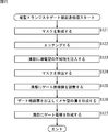
以下、本開示を実施するための形態(以下実施の形態とする)について説明する。なお、説明は以下の順序で行う。
1.第1の実施の形態(撮像素子)
2.第2の実施の形態(製造装置)
3.第3の実施の形態(撮像装置)
4.応用例 Hereinafter, modes for carrying out the present disclosure (hereinafter referred to as embodiments) will be described. The description will be given in the following order.
1. First embodiment (imaging device)
2. Second embodiment (manufacturing apparatus)
3. Third embodiment (imaging apparatus)
4). Application examples
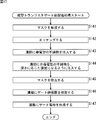
<1.第1の実施の形態>
<縦型トランジスタを有するイメージセンサ>
従来、例えば、特許文献1に記載のイメージセンサのように、光電変換部で光電変換された信号を縦型トランジスタで読み出す撮像素子が考えられた。 <1. First Embodiment>
<Image sensor with vertical transistor>
Conventionally, for example, an image sensor that reads a signal photoelectrically converted by a photoelectric conversion unit with a vertical transistor, such as an image sensor described in Patent Document 1, has been considered.
しかしながら、特許文献1に記載のイメージセンサに用いられる縦型トランジスタは、電荷転送チャネルのポテンシャルが均一であるため、縦型トランジスタのゲート部の長さが長くなる程、電荷を転送する距離が長くなり、電荷を読み出しにくくなるおそれがあった。
However, since the vertical transistor used in the image sensor described in Patent Document 1 has a uniform charge transfer channel potential, the longer the gate length of the vertical transistor, the longer the distance for transferring charges. Therefore, it may be difficult to read out the charge.
<電荷転送チャネルのポテンシャルの勾配>
そこで、撮像素子において、光電変換部からの電荷の読み出しを制御する転送トランジスタとして縦型トランジスタを用い、その縦型トランジスタの、電荷を転送する電荷転送チャネルの少なくとも一部においてポテンシャルが勾配を有するようにする。 <Charge gradient of charge transfer channel>
Therefore, in the imaging device, a vertical transistor is used as a transfer transistor that controls reading of charges from the photoelectric conversion unit, and the potential of the vertical transistor has a gradient in at least a part of the charge transfer channel that transfers charges. To.
このようにすることにより、電荷転送チャネルにおいて電荷をより転送しやすくすることができる。したがって、ノイズの増大を抑制することができ、その撮像素子において得られる撮像画像の画質の低減を抑制することができる。
This makes it easier to transfer charges in the charge transfer channel. Therefore, an increase in noise can be suppressed, and a reduction in image quality of a captured image obtained by the image sensor can be suppressed.
<イメージセンサの画素領域の構成>
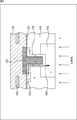
図1は、本技術を適用した撮像素子の一実施の形態であるイメージセンサの画素領域の主な構成例を示す断面図である。図1に示されるイメージセンサ100は、被写体を撮像し、撮像画像を電気信号として得る裏面照射型のCMOS(Complementary Metal Oxide Semiconductor)イメージセンサである。イメージセンサ100は、例えばアレイ状等、面状に配置される複数の画素からなる画素領域を有する。画素領域の各画素において入射光が光電変換され、撮像画像の画素信号が得られる。図1においては、イメージセンサ100のそのような画素領域の一部の積層構造の例が断面図として示されている。図1においては、説明の便宜上、積層構造が模式化して示されている。また、図1においては、本技術の説明に用いられない構成については簡略化若しくは省略されている。 <Configuration of image sensor pixel area>
FIG. 1 is a cross-sectional view illustrating a main configuration example of a pixel region of an image sensor which is an embodiment of an imaging element to which the present technology is applied. Animage sensor 100 illustrated in FIG. 1 is a backside illumination type CMOS (Complementary Metal Oxide Semiconductor) image sensor that captures an image of a subject and obtains a captured image as an electrical signal. The image sensor 100 has a pixel region composed of a plurality of pixels arranged in a planar shape such as an array. Incident light is photoelectrically converted in each pixel of the pixel region, and a pixel signal of a captured image is obtained. In FIG. 1, an example of a laminated structure of a part of such a pixel region of the image sensor 100 is shown as a cross-sectional view. In FIG. 1, for convenience of explanation, a laminated structure is schematically shown. In FIG. 1, configurations that are not used in the description of the present technology are simplified or omitted.
図1は、本技術を適用した撮像素子の一実施の形態であるイメージセンサの画素領域の主な構成例を示す断面図である。図1に示されるイメージセンサ100は、被写体を撮像し、撮像画像を電気信号として得る裏面照射型のCMOS(Complementary Metal Oxide Semiconductor)イメージセンサである。イメージセンサ100は、例えばアレイ状等、面状に配置される複数の画素からなる画素領域を有する。画素領域の各画素において入射光が光電変換され、撮像画像の画素信号が得られる。図1においては、イメージセンサ100のそのような画素領域の一部の積層構造の例が断面図として示されている。図1においては、説明の便宜上、積層構造が模式化して示されている。また、図1においては、本技術の説明に用いられない構成については簡略化若しくは省略されている。 <Configuration of image sensor pixel area>
FIG. 1 is a cross-sectional view illustrating a main configuration example of a pixel region of an image sensor which is an embodiment of an imaging element to which the present technology is applied. An
図1に示されるように、イメージセンサ100は、半導体基板層110を有する。この半導体基板層110は、例えば第1導電型(例えばp型)の半導体基板111と、その半導体基板111に形成される各種構成よりなる。図1に示されるイメージセンサ100は、裏面照射型のイメージセンサであり、図中下側が半導体基板111の表面側であり、図中上側が半導体基板111の裏面側である。
As shown in FIG. 1, the image sensor 100 includes a semiconductor substrate layer 110. The semiconductor substrate layer 110 includes, for example, a first conductivity type (for example, p-type) semiconductor substrate 111 and various configurations formed on the semiconductor substrate 111. An image sensor 100 shown in FIG. 1 is a backside illumination type image sensor.
半導体基板111の内部には、例えば、光電変換部(例えばフォトダイオード)112が形成されている。光電変換部112は、例えば第2導電型(例えばn型)で形成されており、半導体基板の裏面側(すなわち、図中上側)から入射される入射光を光電変換し、得られた電荷を蓄積する。
In the semiconductor substrate 111, for example, a photoelectric conversion unit (for example, a photodiode) 112 is formed. The photoelectric conversion unit 112 is formed of, for example, a second conductivity type (for example, n-type), photoelectrically converts incident light incident from the back side of the semiconductor substrate (that is, the upper side in the figure), and converts the obtained charge into accumulate.
また、半導体基板111には、浮遊拡散層114や絶縁膜115等も形成されている。浮遊拡散層114は、半導体基板111の表側に形成されており、例えば第2導電型(例えばn+型)で形成されている。この浮遊拡散層114は、後述する有機光電変換膜142から転送される電荷を蓄積する。絶縁膜115は、半導体基板111を深さ方向に貫通するように形成されている。
In addition, a floating diffusion layer 114, an insulating film 115, and the like are also formed on the semiconductor substrate 111. The floating diffusion layer 114 is formed on the front side of the semiconductor substrate 111, and is formed of, for example, a second conductivity type (for example, n + type). The floating diffusion layer 114 accumulates charges transferred from the organic photoelectric conversion film 142 described later. The insulating film 115 is formed so as to penetrate the semiconductor substrate 111 in the depth direction.
また、半導体基板111には、転送トランジスタ120も形成されている。転送トランジスタ120は、光電変換部112に蓄積された電荷の浮遊拡散層124への転送を制御するトランジスタであり、縦型トランジスタとして形成されている。転送トランジスタ120は、半導体基板111の表側から光電変換部112に達するようにそのゲート部が形成されている。光電変換部112は、このような転送トランジスタ120のソースとして形成されている。
In addition, a transfer transistor 120 is also formed on the semiconductor substrate 111. The transfer transistor 120 is a transistor that controls the transfer of charges accumulated in the photoelectric conversion unit 112 to the floating diffusion layer 124, and is formed as a vertical transistor. The transfer transistor 120 has a gate portion formed so as to reach the photoelectric conversion portion 112 from the front side of the semiconductor substrate 111. The photoelectric conversion unit 112 is formed as the source of such a transfer transistor 120.
転送トランジスタ120は、例えば、電荷転送チャネル121、ゲート絶縁膜122、ゲート電極123、および浮遊拡散層124を有する。もちろん、これら以外の構成が半導体基板111に形成されてもよい。
The transfer transistor 120 includes, for example, a charge transfer channel 121, a gate insulating film 122, a gate electrode 123, and a floating diffusion layer 124. Of course, configurations other than these may be formed on the semiconductor substrate 111.
電荷転送チャネル121は、転送トランジスタ120のゲート部の構成であり、例えば第1導電型(例えばp+型)に形成されている。電荷転送チャネル121は、光電変換部112と浮遊拡散層124の両方に接続されている。この電荷転送チャネル121に電界が印加されることにより(ゲート電極123の電位に応じて)、光電変換部112の電荷がこの電荷転送チャネル121を介して浮遊拡散層124に伝送される。
The charge transfer channel 121 has a configuration of a gate portion of the transfer transistor 120, and is formed in, for example, a first conductivity type (for example, p + type). The charge transfer channel 121 is connected to both the photoelectric conversion unit 112 and the floating diffusion layer 124. By applying an electric field to the charge transfer channel 121 (according to the potential of the gate electrode 123), the charge of the photoelectric conversion unit 112 is transmitted to the floating diffusion layer 124 via the charge transfer channel 121.
ゲート絶縁膜122は、電荷転送チャネル121の内側に形成されており、絶縁体により形成されており、電荷転送チャネル121とゲート電極123とを電気的に絶縁する層である。
The gate insulating film 122 is formed inside the charge transfer channel 121, is formed of an insulator, and is a layer that electrically insulates the charge transfer channel 121 and the gate electrode 123 from each other.
ゲート電極123は、ゲート電位が印加される電極であり、ゲート絶縁膜122の内側に形成されている。ゲート電極123は、金属等の導体により形成されている。
The gate electrode 123 is an electrode to which a gate potential is applied, and is formed inside the gate insulating film 122. The gate electrode 123 is formed of a conductor such as metal.
浮遊拡散層124は、半導体基板111の表側に形成されている。浮遊拡散層124は、例えば第2導電型(例えばn+型)で形成されている。浮遊拡散層124は、転送トランジスタ120のドレインとして形成されている。この浮遊拡散層124は、光電変換部112から転送される電荷を蓄積する。
The floating diffusion layer 124 is formed on the front side of the semiconductor substrate 111. The floating diffusion layer 124 is formed of, for example, a second conductivity type (for example, n + type). The floating diffusion layer 124 is formed as the drain of the transfer transistor 120. The floating diffusion layer 124 accumulates charges transferred from the photoelectric conversion unit 112.
半導体基板層110の表面側には、配線層130が形成されている。配線層130には、配線層間膜131と、配線132や配線133等の配線とが形成されている。配線層間膜131は、絶縁体により形成されており、金属等の導体よりなる配線同士を電気的に絶縁する層である。
A wiring layer 130 is formed on the surface side of the semiconductor substrate layer 110. In the wiring layer 130, a wiring interlayer film 131 and wirings such as the wiring 132 and the wiring 133 are formed. The wiring interlayer film 131 is formed of an insulator and is a layer that electrically insulates wirings made of a conductor such as metal.
なお、配線132および配線133は、配線層130に形成される配線の例を示したものであり、実際には、配線層130には、配線132および配線133以外の配線も形成される。例えば、ゲート電極123は、図示せぬコンタクト等を介して図示せぬ配線(制御線等)に接続されている。ゲート電極123は、その制御線を介して供給される信号に応じた電位を有する(信号に応じた電界を電荷転送チャネル121に印加する)。
Note that the wiring 132 and the wiring 133 are examples of wiring formed in the wiring layer 130, and actually, wiring other than the wiring 132 and the wiring 133 is also formed in the wiring layer 130. For example, the gate electrode 123 is connected to a wiring (control line or the like) not shown through a contact or the like (not shown). The gate electrode 123 has a potential corresponding to a signal supplied via the control line (an electric field corresponding to the signal is applied to the charge transfer channel 121).
また、浮遊拡散層124は、例えば、図示せぬコンタクト等を介して図示せぬ配線に接続されている。同様に、浮遊拡散層114は、例えば、図示せぬコンタクト等を介して図示せぬ配線に接続されている。浮遊拡散層114や浮遊拡散層124に蓄積された電荷は、その配線を介して、例えば図示せぬ増幅トランジスタのゲート等に供給される。
The floating diffusion layer 124 is connected to a wiring (not shown) via, for example, a contact (not shown). Similarly, the floating diffusion layer 114 is connected to a wiring (not shown) via, for example, a contact (not shown). The charges accumulated in the floating diffusion layer 114 and the floating diffusion layer 124 are supplied to, for example, a gate of an amplification transistor (not shown) through the wiring.
半導体基板層110の裏面側には、絶縁膜141と有機光電変換膜142が積層されている。有機光電変換膜142の光電変換部112近傍の表面側には、下部透明電極143が形成されている。また、有機光電変換膜142の裏面側には、上部透明電極144が形成されている。下部透明電極143は、絶縁膜115内部に形成される貫通電極145を介して配線133に接続されている。また、浮遊拡散層114は、コンタクト146を介して配線133に接続されている。つまり、有機光電変換膜142は、下部透明電極143、貫通電極145、配線133、およびコンタクト146を介して浮遊拡散層114に接続されている。有機光電変換膜142において入射光が光電変換されて得られた電荷は、下部透明電極143、貫通電極145、配線133、およびコンタクト146を介して浮遊拡散層114に供給される。
On the back side of the semiconductor substrate layer 110, an insulating film 141 and an organic photoelectric conversion film 142 are stacked. A lower transparent electrode 143 is formed on the surface side of the organic photoelectric conversion film 142 in the vicinity of the photoelectric conversion unit 112. An upper transparent electrode 144 is formed on the back side of the organic photoelectric conversion film 142. The lower transparent electrode 143 is connected to the wiring 133 through a through electrode 145 formed inside the insulating film 115. The floating diffusion layer 114 is connected to the wiring 133 through the contact 146. That is, the organic photoelectric conversion film 142 is connected to the floating diffusion layer 114 via the lower transparent electrode 143, the through electrode 145, the wiring 133, and the contact 146. The charge obtained by photoelectric conversion of incident light in the organic photoelectric conversion film 142 is supplied to the floating diffusion layer 114 via the lower transparent electrode 143, the through electrode 145, the wiring 133, and the contact 146.
上部透明電極144の裏面側には、パッシベーション層151が形成されている。パッシベーション層151は、例えばSiN等により形成され、パッシベーション層151より表面側の各層(例えば、上部透明電極144等)を保護する。
A passivation layer 151 is formed on the back side of the upper transparent electrode 144. The passivation layer 151 is formed of SiN or the like, for example, and protects each layer (for example, the upper transparent electrode 144 and the like) on the surface side of the passivation layer 151.
パッシベーション層151の裏面側には、各画素に入射する入射光を光電変換部112等に集光するオンチップレンズ152が形成されている。
On the back surface side of the passivation layer 151, an on-chip lens 152 for condensing incident light incident on each pixel on the photoelectric conversion unit 112 or the like is formed.
<電荷転送方向のポテンシャル勾配>
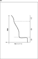
以上のような構成の画素を有するイメージセンサ100において、例えば図2のように、電荷転送チャネル121における電荷転送方向(図2中の矢印161の方向の逆向き)に、電荷の転送先に向かって深くなるようなポテンシャルの勾配(電位勾配)が形成されるようにしてもよい。 <Potential gradient in charge transfer direction>
In theimage sensor 100 having the pixels configured as described above, for example, as shown in FIG. 2, the charge transfer direction in the charge transfer channel 121 (opposite to the direction of the arrow 161 in FIG. 2) is directed toward the charge transfer destination. A potential gradient (potential gradient) may be formed so as to be deeper.
以上のような構成の画素を有するイメージセンサ100において、例えば図2のように、電荷転送チャネル121における電荷転送方向(図2中の矢印161の方向の逆向き)に、電荷の転送先に向かって深くなるようなポテンシャルの勾配(電位勾配)が形成されるようにしてもよい。 <Potential gradient in charge transfer direction>
In the
なお、転送トランジスタ120が縦型トランジスタであるので、図2に示されるように、例えば、電荷転送チャネル121の、ゲート電極123の側壁部分に相当する部分においては、この電荷転送方向は、半導体基板111の深さ方向(図中下から上に向かう方向)となる。
Since the transfer transistor 120 is a vertical transistor, as shown in FIG. 2, for example, in the portion corresponding to the side wall portion of the gate electrode 123 of the charge transfer channel 121, the charge transfer direction is the same as that of the semiconductor substrate. The depth direction is 111 (the direction from the bottom to the top in the figure).
図2の浮遊拡散層124から電荷転送チャネル121を介して光電変換部112に向かう矢印161が示す方向のポテンシャルの分布の様子の例を、図3に示す。図3に示されるグラフでは、横軸が矢印161の各位置を示し、縦軸がポテンシャルの深さを示している。図3のグラフに示されるように、電荷転送チャネル121のポテンシャルは、この矢印161にそって、浮遊拡散層124に近づくほど深くなっている。つまり、ポテンシャルが、電荷転送チャネル121の少なくとも一部において勾配を有している。
FIG. 3 shows an example of the potential distribution in the direction indicated by the arrow 161 directed from the floating diffusion layer 124 of FIG. 2 to the photoelectric conversion unit 112 via the charge transfer channel 121. In the graph shown in FIG. 3, the horizontal axis indicates each position indicated by the arrow 161, and the vertical axis indicates the potential depth. As shown in the graph of FIG. 3, the potential of the charge transfer channel 121 becomes deeper toward the floating diffusion layer 124 along the arrow 161. That is, the potential has a gradient in at least a part of the charge transfer channel 121.
このように、電荷転送方向に、電荷の転送先に向かって深くなるような電位勾配をつけることにより、光電変換部112から浮遊拡散層124への電荷転送をより容易にすることができる。
As described above, by providing a potential gradient deeper in the charge transfer direction toward the charge transfer destination, charge transfer from the photoelectric conversion unit 112 to the floating diffusion layer 124 can be facilitated.
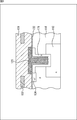
<ゲート絶縁膜の膜厚制御1>
次に、以上のように電荷転送方向にポテンシャルの勾配を形成する具体例を説明する。ゲート絶縁膜の膜厚が、電荷の転送先に向かって漸次薄くなるように形成されるようにしてもよい。例えば、図4に示されるように、ゲート絶縁膜122の膜厚が、電荷の転送先(浮遊拡散層124)に向かって漸次薄くなるように形成されるようにしてもよい。 <Gate insulation film thickness control 1>
Next, a specific example of forming a potential gradient in the charge transfer direction as described above will be described. The gate insulating film may be formed so that its thickness gradually decreases toward the charge transfer destination. For example, as illustrated in FIG. 4, thegate insulating film 122 may be formed so that the film thickness gradually decreases toward the charge transfer destination (floating diffusion layer 124).
次に、以上のように電荷転送方向にポテンシャルの勾配を形成する具体例を説明する。ゲート絶縁膜の膜厚が、電荷の転送先に向かって漸次薄くなるように形成されるようにしてもよい。例えば、図4に示されるように、ゲート絶縁膜122の膜厚が、電荷の転送先(浮遊拡散層124)に向かって漸次薄くなるように形成されるようにしてもよい。 <Gate insulation film thickness control 1>
Next, a specific example of forming a potential gradient in the charge transfer direction as described above will be described. The gate insulating film may be formed so that its thickness gradually decreases toward the charge transfer destination. For example, as illustrated in FIG. 4, the
図4の例においては、ゲート電極123が、電荷の転送先に向かって漸次太くなるように形成されており(半導体基板111の深さ方向に、裏面側に向かって漸次細くなるように形成されており)、その分、ゲート絶縁膜122の膜厚が、電荷の転送先に向かって漸次薄くなっている。
In the example of FIG. 4, the gate electrode 123 is formed so as to gradually become thicker toward the charge transfer destination (formed so as to become gradually thinner toward the back surface side in the depth direction of the semiconductor substrate 111. Accordingly, the thickness of the gate insulating film 122 is gradually reduced toward the charge transfer destination.
このようにすることにより、電荷転送チャネル121に印加される電界を、浮遊拡散層124により近くなる程、強くすることができる。したがって、電荷転送チャネル121(特に、電荷転送チャネル121の、ゲート電極123の側壁部分に相当する部分)において、ポテンシャルが、図3の例のように、浮遊拡散層124に近づくほど深くなるようにすることができる。このようにすることにより、光電変換部112から浮遊拡散層124への電荷転送をより容易にすることができる。
By doing so, the electric field applied to the charge transfer channel 121 can be strengthened as it is closer to the floating diffusion layer 124. Therefore, in the charge transfer channel 121 (particularly, the portion corresponding to the side wall portion of the gate electrode 123 of the charge transfer channel 121), the potential becomes deeper as it approaches the floating diffusion layer 124 as in the example of FIG. can do. In this way, charge transfer from the photoelectric conversion unit 112 to the floating diffusion layer 124 can be facilitated.
<ゲート絶縁膜の膜厚制御2>
また、ゲート絶縁膜の膜厚が、電荷の転送先に向かって階段状に薄くなるように形成されるようにしてもよい。例えば、図5に示されるように、ゲート絶縁膜122の膜厚が、電荷の転送先(浮遊拡散層124)に向かって階段状に薄くなるように形成されるようにしてもよい。 <Gate insulation film thickness control 2>
Alternatively, the gate insulating film may be formed so as to be thin in a stepped manner toward the charge transfer destination. For example, as shown in FIG. 5, thegate insulating film 122 may be formed so that the thickness thereof decreases in a stepped manner toward the charge transfer destination (floating diffusion layer 124).
また、ゲート絶縁膜の膜厚が、電荷の転送先に向かって階段状に薄くなるように形成されるようにしてもよい。例えば、図5に示されるように、ゲート絶縁膜122の膜厚が、電荷の転送先(浮遊拡散層124)に向かって階段状に薄くなるように形成されるようにしてもよい。 <Gate insulation film thickness control 2>
Alternatively, the gate insulating film may be formed so as to be thin in a stepped manner toward the charge transfer destination. For example, as shown in FIG. 5, the
図5の例においては、ゲート電極123が、電荷の転送先に向かって階段状に太くなるように形成されており(半導体基板111の深さ方向に、裏面側に向かって階段状に細くなるように形成されており)、その分、ゲート絶縁膜122の膜厚が、電荷の転送先に向かって階段状に薄くなっている。
In the example of FIG. 5, the gate electrode 123 is formed so as to increase in a staircase pattern toward the charge transfer destination (in a depth direction of the semiconductor substrate 111, it decreases in a staircase pattern toward the back surface side. Accordingly, the thickness of the gate insulating film 122 is reduced stepwise toward the charge transfer destination.
このようにすることにより、電荷転送チャネル121に印加される電界を、浮遊拡散層124により近くなる程、強くすることができる。したがって、電荷転送チャネル121(特に、電荷転送チャネル121の、ゲート電極123の側壁部分に相当する部分)において、ポテンシャルが、図3の例のように、浮遊拡散層124に近づくほど深くなるようにすることができる。このようにすることにより、光電変換部112から浮遊拡散層124への電荷転送をより容易にすることができる。
By doing so, the electric field applied to the charge transfer channel 121 can be strengthened as it is closer to the floating diffusion layer 124. Therefore, in the charge transfer channel 121 (particularly, the portion corresponding to the side wall portion of the gate electrode 123 of the charge transfer channel 121), the potential becomes deeper as it approaches the floating diffusion layer 124 as in the example of FIG. can do. In this way, charge transfer from the photoelectric conversion unit 112 to the floating diffusion layer 124 can be facilitated.
<ゲート絶縁膜の膜厚制御3>
なお、転送トランジスタの電荷転送チャネルは、第2導電型(例えば、n型)で形成されるようにしてもよい。例えば、図6に示されるように、転送トランジスタ120の電荷転送チャネル171が、第2導電型(例えば、n型)で形成されるようにしてもよい。図6の例のイメージセンサ100の場合、電荷転送チャネル121の代わりに電荷転送チャネル171が形成されている。電荷転送チャネル171は、転送トランジスタ120のゲート部の構成であり、例えば第2導電型(例えばn型)に形成されている。電荷転送チャネル171は、光電変換部112と浮遊拡散層124の両方に接続されている。この電荷転送チャネル171に電界が印加されることにより(ゲート電極123の電位に応じて)、光電変換部112の電荷がこの電荷転送チャネル171を介して浮遊拡散層124に伝送される。 <Gate insulation film thickness control 3>
Note that the charge transfer channel of the transfer transistor may be formed of the second conductivity type (for example, n-type). For example, as shown in FIG. 6, thecharge transfer channel 171 of the transfer transistor 120 may be formed of the second conductivity type (for example, n-type). In the case of the image sensor 100 in the example of FIG. 6, a charge transfer channel 171 is formed instead of the charge transfer channel 121. The charge transfer channel 171 has a configuration of a gate portion of the transfer transistor 120 and is formed, for example, in the second conductivity type (for example, n-type). The charge transfer channel 171 is connected to both the photoelectric conversion unit 112 and the floating diffusion layer 124. By applying an electric field to the charge transfer channel 171 (according to the potential of the gate electrode 123), the charge of the photoelectric conversion unit 112 is transmitted to the floating diffusion layer 124 via the charge transfer channel 171.
なお、転送トランジスタの電荷転送チャネルは、第2導電型(例えば、n型)で形成されるようにしてもよい。例えば、図6に示されるように、転送トランジスタ120の電荷転送チャネル171が、第2導電型(例えば、n型)で形成されるようにしてもよい。図6の例のイメージセンサ100の場合、電荷転送チャネル121の代わりに電荷転送チャネル171が形成されている。電荷転送チャネル171は、転送トランジスタ120のゲート部の構成であり、例えば第2導電型(例えばn型)に形成されている。電荷転送チャネル171は、光電変換部112と浮遊拡散層124の両方に接続されている。この電荷転送チャネル171に電界が印加されることにより(ゲート電極123の電位に応じて)、光電変換部112の電荷がこの電荷転送チャネル171を介して浮遊拡散層124に伝送される。 <Gate insulation film thickness control 3>
Note that the charge transfer channel of the transfer transistor may be formed of the second conductivity type (for example, n-type). For example, as shown in FIG. 6, the
このような第2導電型(例えばn型)の電荷転送チャネルを有する転送トランジスタにおいて、ゲート絶縁膜の膜厚が、電荷の転送先に向かって漸次厚くなるように形成されるようにしてもよい。例えば、図6に示されるように、転送トランジスタ120において、ゲート絶縁膜122の膜厚が、電荷の転送先(浮遊拡散層124)に向かって漸次厚くなるように形成されるようにしてもよい。
In such a transfer transistor having a second conductivity type (for example, n-type) charge transfer channel, the gate insulating film may be formed so that its thickness gradually increases toward the charge transfer destination. . For example, as shown in FIG. 6, in the transfer transistor 120, the gate insulating film 122 may be formed so that the film thickness gradually increases toward the charge transfer destination (floating diffusion layer 124). .
図6の例においては、ゲート電極123が、電荷の転送先に向かって漸次細くなるように形成されており(半導体基板111の深さ方向に、裏面側に向かって漸次太くなるように形成されており)、その分、ゲート絶縁膜122の膜厚が、電荷の転送先に向かって漸次厚くなっている。
In the example of FIG. 6, the gate electrode 123 is formed so as to become gradually thinner toward the charge transfer destination (formed so as to become gradually thicker toward the back surface side in the depth direction of the semiconductor substrate 111). Accordingly, the thickness of the gate insulating film 122 gradually increases toward the charge transfer destination.
このようにすることにより、電荷転送チャネル171に印加される電界を、浮遊拡散層124により近くなる程、強くすることができる。したがって、電荷転送チャネル171(特に、電荷転送チャネル171の、ゲート電極123の側壁部分に相当する部分)において、ポテンシャルが、図3の例のように、浮遊拡散層124に近づくほど深くなるようにすることができる。このようにすることにより、光電変換部112から浮遊拡散層124への電荷転送をより容易にすることができる。
By doing so, the electric field applied to the charge transfer channel 171 can be strengthened as it is closer to the floating diffusion layer 124. Therefore, in the charge transfer channel 171 (particularly, the portion corresponding to the side wall portion of the gate electrode 123 of the charge transfer channel 171), the potential becomes deeper as it approaches the floating diffusion layer 124 as in the example of FIG. can do. In this way, charge transfer from the photoelectric conversion unit 112 to the floating diffusion layer 124 can be facilitated.
<ゲート絶縁膜の膜厚制御4>
また、ゲート絶縁膜の膜厚が、電荷の転送先に向かって階段状に厚くなるように形成されるようにしてもよい。例えば、図7に示されるように、ゲート絶縁膜122の膜厚が、電荷の転送先(浮遊拡散層124)に向かって階段状に厚くなるように形成されるようにしてもよい。 <Gate insulation film thickness control 4>
Alternatively, the gate insulating film may be formed so as to increase in a stepped manner toward the charge transfer destination. For example, as shown in FIG. 7, thegate insulating film 122 may be formed so that the thickness thereof increases stepwise toward the charge transfer destination (floating diffusion layer 124).
また、ゲート絶縁膜の膜厚が、電荷の転送先に向かって階段状に厚くなるように形成されるようにしてもよい。例えば、図7に示されるように、ゲート絶縁膜122の膜厚が、電荷の転送先(浮遊拡散層124)に向かって階段状に厚くなるように形成されるようにしてもよい。 <Gate insulation film thickness control 4>
Alternatively, the gate insulating film may be formed so as to increase in a stepped manner toward the charge transfer destination. For example, as shown in FIG. 7, the
図7の例においては、ゲート電極123が、電荷の転送先に向かって階段状に細くなるように形成されており(半導体基板111の深さ方向に、裏面側に向かって階段状に太くなるように形成されており)、その分、ゲート絶縁膜122の膜厚が、電荷の転送先に向かって階段状に厚くなっている。
In the example of FIG. 7, the gate electrode 123 is formed to be thin in a staircase pattern toward the charge transfer destination (in a depth direction of the semiconductor substrate 111, it is thickened in a staircase pattern toward the back surface side. Accordingly, the thickness of the gate insulating film 122 is increased stepwise toward the charge transfer destination.
このようにすることにより、電荷転送チャネル171に印加される電界を、浮遊拡散層124により近くなる程、強くすることができる。したがって、電荷転送チャネル171(特に、電荷転送チャネル171の、ゲート電極123の側壁部分に相当する部分)において、ポテンシャルが、図3の例のように、浮遊拡散層124に近づくほど深くなるようにすることができる。このようにすることにより、光電変換部112から浮遊拡散層124への電荷転送をより容易にすることができる。
By doing so, the electric field applied to the charge transfer channel 171 can be strengthened as it is closer to the floating diffusion layer 124. Therefore, in the charge transfer channel 171 (particularly, the portion corresponding to the side wall portion of the gate electrode 123 of the charge transfer channel 171), the potential becomes deeper as it approaches the floating diffusion layer 124 as in the example of FIG. can do. In this way, charge transfer from the photoelectric conversion unit 112 to the floating diffusion layer 124 can be facilitated.
<電荷転送チャネルの不純物濃度制御>
また、転送トランジスタの電荷転送チャネルが、第1導電型(例えば、p型)で形成される場合、その電荷転送チャネルが、電荷の転送先に向かって不純物濃度が薄くなるように形成されるようにしてもよい。例えば、図8に示されるように、電荷転送チャネル121に注入された不純物の濃度が、電荷の転送先(浮遊拡散層124)に向かって薄くなるようにしてもよい。 <Impurity control of charge transfer channel>
Further, when the charge transfer channel of the transfer transistor is formed of the first conductivity type (for example, p-type), the charge transfer channel is formed so that the impurity concentration decreases toward the charge transfer destination. It may be. For example, as shown in FIG. 8, the concentration of the impurity injected into thecharge transfer channel 121 may be reduced toward the charge transfer destination (floating diffusion layer 124).
また、転送トランジスタの電荷転送チャネルが、第1導電型(例えば、p型)で形成される場合、その電荷転送チャネルが、電荷の転送先に向かって不純物濃度が薄くなるように形成されるようにしてもよい。例えば、図8に示されるように、電荷転送チャネル121に注入された不純物の濃度が、電荷の転送先(浮遊拡散層124)に向かって薄くなるようにしてもよい。 <Impurity control of charge transfer channel>
Further, when the charge transfer channel of the transfer transistor is formed of the first conductivity type (for example, p-type), the charge transfer channel is formed so that the impurity concentration decreases toward the charge transfer destination. It may be. For example, as shown in FIG. 8, the concentration of the impurity injected into the
図8の例においては、電荷転送チャネル121に注入された不純物の濃度が、電荷の転送先(浮遊拡散層124)に向かって階段状に薄くなっている。すなわち、不純物の濃度は、電荷転送チャネル121-1(p+)>電荷転送チャネル121-2(p)>電荷転送チャネル121-3(p-)である。
In the example of FIG. 8, the concentration of the impurity implanted into the charge transfer channel 121 decreases in a staircase pattern toward the charge transfer destination (floating diffusion layer 124). That is, the impurity concentration is charge transfer channel 121-1 (p + )> charge transfer channel 121-2 (p)> charge transfer channel 121-3 (p−).
このようにすることにより、電荷転送チャネル121のポテンシャルが、図3の例のように、浮遊拡散層124に近づくほど深くなるようにすることができる。このようにすることにより、光電変換部112から浮遊拡散層124への電荷転送をより容易にすることができる。
By doing so, the potential of the charge transfer channel 121 can be made deeper as it approaches the floating diffusion layer 124 as in the example of FIG. In this way, charge transfer from the photoelectric conversion unit 112 to the floating diffusion layer 124 can be facilitated.
なお、この電荷転送チャネル121に注入される不純物の濃度は、電荷の転送先(浮遊拡散層124)に向かって漸次薄くなるようにしてもよい。
Note that the concentration of the impurity injected into the charge transfer channel 121 may be gradually reduced toward the charge transfer destination (floating diffusion layer 124).
また、電荷転送チャネルが、第2導電型(例えば、n型)の場合も同様に不純物の濃度を制御するようにしてもよい。例えば、第2導電型(例えば、n型)の電荷転送チャネル171に注入された不純物の濃度が、電荷の転送先(浮遊拡散層124)に向かって濃くなるようにしてもよい。その場合、不純物の濃度は、電荷の転送先(浮遊拡散層124)に向かって階段状に濃くなるようにしてもよいし、電荷の転送先(浮遊拡散層124)に向かって漸次濃くなるようにしてもよい。
Also, the impurity concentration may be controlled similarly when the charge transfer channel is of the second conductivity type (for example, n-type). For example, the concentration of impurities injected into the second conductivity type (for example, n-type) charge transfer channel 171 may be increased toward the charge transfer destination (floating diffusion layer 124). In that case, the impurity concentration may be increased stepwise toward the charge transfer destination (floating diffusion layer 124) or gradually increased toward the charge transfer destination (floating diffusion layer 124). It may be.
<回転方向のポテンシャル勾配>
以上のような構成の画素を有するイメージセンサにおいて、電荷転送チャネルにおけるゲート電極に沿った回転方向にポテンシャルの勾配(電位勾配)が形成されるようにしてもよい。 <Potential gradient in rotation direction>
In the image sensor having the pixel configured as described above, a potential gradient (potential gradient) may be formed in the rotation direction along the gate electrode in the charge transfer channel.
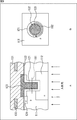
例えば、図9のAに示される転送トランジスタ120のゲート部の、点線181における水平方向の断面図を図9のBに示す。図9のBに示される矢印182は、ゲート部の電荷転送チャネル121における、ゲート電極123に沿った、ゲート電極123を周回する回転方向を示している。
For example, FIG. 9B shows a horizontal sectional view taken along the dotted line 181 of the gate portion of the transfer transistor 120 shown in FIG. 9A. An arrow 182 shown in FIG. 9B indicates the direction of rotation around the gate electrode 123 along the gate electrode 123 in the charge transfer channel 121 of the gate portion.
この矢印182が示す方向のポテンシャルの分布の様子の例を、図10に示す。図10に示されるグラフでは、横軸が矢印182の各位置を示し、縦軸がポテンシャルの深さを示している。図10のグラフに示されるように、電荷転送チャネル121のポテンシャルは、この矢印182にそって変化する。つまり、電荷転送チャネル121のポテンシャルは、この矢印182の方向の少なくとも一部において、その矢印182の方向に勾配を有する。
An example of the potential distribution in the direction indicated by the arrow 182 is shown in FIG. In the graph shown in FIG. 10, the horizontal axis indicates each position of the arrow 182, and the vertical axis indicates the potential depth. As shown in the graph of FIG. 10, the potential of the charge transfer channel 121 changes along this arrow 182. That is, the potential of the charge transfer channel 121 has a gradient in the direction of the arrow 182 in at least a part of the direction of the arrow 182.
このように、電荷転送チャネル121において回転方向に電位勾配をつけることにより、電荷は、電荷転送チャネル121のポテンシャルの低い部分に集中して、光電変換部112から浮遊拡散層124に転送されるようになる。これにより、光電変換部112から浮遊拡散層124に電荷をより転送しやすくすることができる。
In this way, by applying a potential gradient in the rotation direction in the charge transfer channel 121, the charge is concentrated on the low potential portion of the charge transfer channel 121 and transferred from the photoelectric conversion unit 112 to the floating diffusion layer 124. become. This makes it easier to transfer charges from the photoelectric conversion unit 112 to the floating diffusion layer 124.
<ゲート絶縁膜の膜厚制御>
次に、以上のように電荷転送方向にポテンシャルの勾配を形成する具体例を説明する。ゲート絶縁膜の膜厚が、ゲート電極に沿った回転方向に変化するようにしてもよい。つまり、上述した矢印182で示される回転方向にゲート絶縁膜122の膜厚が変化する(偏りを有する)ようにしてもよい。例えば、上述した矢印182で示される回転方向の一部において、ゲート絶縁膜122の膜厚が、他の部分と異なる(他の部分よりも厚い、若しくは、薄い)ようにしてもよい。 <Gate insulation film thickness control>
Next, a specific example of forming a potential gradient in the charge transfer direction as described above will be described. The thickness of the gate insulating film may be changed in the rotation direction along the gate electrode. That is, the thickness of thegate insulating film 122 may change (have a bias) in the rotation direction indicated by the arrow 182 described above. For example, the gate insulating film 122 may have a different film thickness (thicker or thinner than the other portions) in a part of the rotation direction indicated by the arrow 182 described above.
次に、以上のように電荷転送方向にポテンシャルの勾配を形成する具体例を説明する。ゲート絶縁膜の膜厚が、ゲート電極に沿った回転方向に変化するようにしてもよい。つまり、上述した矢印182で示される回転方向にゲート絶縁膜122の膜厚が変化する(偏りを有する)ようにしてもよい。例えば、上述した矢印182で示される回転方向の一部において、ゲート絶縁膜122の膜厚が、他の部分と異なる(他の部分よりも厚い、若しくは、薄い)ようにしてもよい。 <Gate insulation film thickness control>
Next, a specific example of forming a potential gradient in the charge transfer direction as described above will be described. The thickness of the gate insulating film may be changed in the rotation direction along the gate electrode. That is, the thickness of the
例えば、図11のAに示されるように、ゲート電極123の中心の位置を、ゲート絶縁膜122の中心の位置からずらすことにより、矢印182で示される回転方向にゲート絶縁膜122の膜厚の偏りを生じさせるようにしてもよい。
For example, as illustrated in FIG. 11A, by shifting the center position of the gate electrode 123 from the center position of the gate insulating film 122, the thickness of the gate insulating film 122 is increased in the rotation direction indicated by the arrow 182. You may make it produce bias.
また、例えば、図11のBに示されるように、ゲート電極123の断面形状を、ゲート絶縁膜122の断面形状と異なる形状とすることにより、矢印182で示される回転方向にゲート絶縁膜122の膜厚の偏りを生じさせるようにしてもよい。
For example, as shown in FIG. 11B, the gate electrode 123 has a cross-sectional shape different from the cross-sectional shape of the gate insulating film 122, whereby the gate insulating film 122 is rotated in the rotation direction indicated by the arrow 182. You may make it produce the nonuniformity of a film thickness.
なお、この回転方向の膜厚の変化(偏り)は、漸次であってもよいし、階段状であってもよい。
In addition, the change (bias) of the film thickness in the rotation direction may be gradual or may be stepped.
<電荷転送チャネルの不純物濃度制御>
また、転送トランジスタの電荷転送チャネルが、電荷転送チャネルにおけるゲート電極に沿った回転方向に不純物濃度が変化するように形成されるようにしてもよい。例えば、図11のCに示されるように、電荷転送チャネル121に注入された不純物の濃度が、ゲート電極に沿った回転方向(矢印182)に変化するようにしてもよい。 <Impurity control of charge transfer channel>
Further, the charge transfer channel of the transfer transistor may be formed so that the impurity concentration changes in the rotation direction along the gate electrode in the charge transfer channel. For example, as shown in FIG. 11C, the concentration of the impurity injected into thecharge transfer channel 121 may change in the rotation direction (arrow 182) along the gate electrode.
また、転送トランジスタの電荷転送チャネルが、電荷転送チャネルにおけるゲート電極に沿った回転方向に不純物濃度が変化するように形成されるようにしてもよい。例えば、図11のCに示されるように、電荷転送チャネル121に注入された不純物の濃度が、ゲート電極に沿った回転方向(矢印182)に変化するようにしてもよい。 <Impurity control of charge transfer channel>
Further, the charge transfer channel of the transfer transistor may be formed so that the impurity concentration changes in the rotation direction along the gate electrode in the charge transfer channel. For example, as shown in FIG. 11C, the concentration of the impurity injected into the
図11のCの例においては、電荷転送チャネル121に注入された不純物の濃度が、電荷の転送先(浮遊拡散層124)に向かって階段状に薄くなっている。すなわち、不純物の濃度は、電荷転送チャネル121-1(p+)>電荷転送チャネル121-2(p)>電荷転送チャネル121-3(p-)である。
In the example of FIG. 11C, the concentration of the impurity injected into the charge transfer channel 121 is reduced stepwise toward the charge transfer destination (floating diffusion layer 124). That is, the impurity concentration is charge transfer channel 121-1 (p +)> charge transfer channel 121-2 (p)> charge transfer channel 121-3 (p-).
このようにすることにより、電荷は、電荷転送チャネル121のポテンシャルの低い部分に集中して、光電変換部112から浮遊拡散層124に転送されるようになる。これにより、光電変換部112から浮遊拡散層124に電荷をより転送しやすくすることができる。
By doing so, the charges are concentrated on the low potential portion of the charge transfer channel 121 and transferred from the photoelectric conversion unit 112 to the floating diffusion layer 124. This makes it easier to transfer charges from the photoelectric conversion unit 112 to the floating diffusion layer 124.
なお、この電荷転送チャネル121に注入される不純物の濃度は、矢印182に沿って漸次薄くなるようにしてもよい。
Note that the concentration of the impurity injected into the charge transfer channel 121 may be gradually decreased along the arrow 182.
また、電荷転送チャネルが、第2導電型(例えば、n型)の場合も同様に、ゲート絶縁膜122の膜厚や不純物の濃度が、ゲート電極に沿った回転方向に変化するようにしてもよい。つまり、図6や図7の例のように、電荷転送チャネル121の代わりに電荷転送チャネル171を有するようにしてもよく、その場合も、上述したように、ゲート絶縁膜122の膜厚や不純物の濃度を、ゲート電極に沿った回転方向に変化させるようにしてもよい。
Similarly, when the charge transfer channel is of the second conductivity type (for example, n-type), the thickness of the gate insulating film 122 and the concentration of impurities may be changed in the rotation direction along the gate electrode. Good. That is, as in the examples of FIGS. 6 and 7, the charge transfer channel 171 may be provided instead of the charge transfer channel 121. In this case, as described above, the thickness of the gate insulating film 122 and the impurities The concentration may be changed in the direction of rotation along the gate electrode.
このようにすることにより、電荷転送チャネル121の場合と同様に、電荷が、電荷転送チャネル121のポテンシャルの低い部分に集中して、光電変換部112から浮遊拡散層124に転送されるようになる。これにより、光電変換部112から浮遊拡散層124に電荷をより転送しやすくすることができる。
By doing so, as in the case of the charge transfer channel 121, the charges are concentrated on the low potential portion of the charge transfer channel 121 and transferred from the photoelectric conversion unit 112 to the floating diffusion layer 124. . This makes it easier to transfer charges from the photoelectric conversion unit 112 to the floating diffusion layer 124.
<2.第2の実施の形態>
<製造装置>
次に、以上に説明したようなイメージセンサ100の製造について説明する。 <2. Second Embodiment>
<Manufacturing equipment>
Next, the manufacture of theimage sensor 100 as described above will be described.
<製造装置>
次に、以上に説明したようなイメージセンサ100の製造について説明する。 <2. Second Embodiment>
<Manufacturing equipment>
Next, the manufacture of the
図12は、本技術を適用した撮像素子の一実施の形態であるイメージセンサ100を製造する製造装置(本技術を適用した製造装置の一実施の形態である製造装置)の主な構成例を示すブロック図である。図12に示される製造装置200は、制御部201およびイメージセンサ製造部202を有する。
FIG. 12 is a main configuration example of a manufacturing apparatus that manufactures an image sensor 100 that is an embodiment of an imaging device to which the present technology is applied (a manufacturing apparatus that is an embodiment of a manufacturing apparatus to which the present technology is applied). FIG. A manufacturing apparatus 200 illustrated in FIG. 12 includes a control unit 201 and an image sensor manufacturing unit 202.
制御部201は、例えば、CPU(Central Processing Unit)、ROM(Read Only Memory)、およびRAM(Random Access Memory)等を有し、イメージセンサ製造部202の各部を制御し、イメージセンサ100の製造に関する制御処理を行う。例えば、制御部201のCPUは、ROMに記憶されているプログラムに従って各種の処理を実行する。また、そのCPUは、記憶部213からRAMにロードされたプログラムに従って各種の処理を実行する。RAMにはまた、CPUが各種の処理を実行するにあたって必要なデータなども適宜記憶される。
The control unit 201 includes, for example, a CPU (Central Processing Unit), a ROM (Read Only Memory), a RAM (Random Access Memory), and the like, and controls each unit of the image sensor manufacturing unit 202 and relates to the manufacture of the image sensor 100. Perform control processing. For example, the CPU of the control unit 201 executes various processes according to programs stored in the ROM. Further, the CPU executes various processes according to programs loaded from the storage unit 213 to the RAM. The RAM also appropriately stores data necessary for the CPU to execute various processes.
イメージセンサ製造部202は、制御部201に制御されて、イメージセンサ100の製造に関する処理を行う。つまり、実際には、イメージセンサ製造部202は、イメージセンサ100を製造する全ての工程に関する処理を行う。例えば、イメージセンサ製造部202は、半導体基板層110や配線層130の各構成を形成したり、半導体基板層110の裏面側の構成(絶縁膜141乃至オンチップレンズ152等)を形成したりする。ただし、以下においては、説明の便宜上、転送トランジスタ120のゲート部の製造に関する部分についてのみ説明する。
The image sensor manufacturing unit 202 is controlled by the control unit 201 to perform processing related to manufacturing of the image sensor 100. That is, in practice, the image sensor manufacturing unit 202 performs processing relating to all processes for manufacturing the image sensor 100. For example, the image sensor manufacturing unit 202 forms each configuration of the semiconductor substrate layer 110 and the wiring layer 130 or forms a configuration on the back side of the semiconductor substrate layer 110 (such as the insulating film 141 to the on-chip lens 152). . However, in the following, for convenience of explanation, only the part relating to the manufacture of the gate part of the transfer transistor 120 will be described.
イメージセンサ製造部202は、例えば、縦型トランジスタ製造部231を有する。縦型トランジスタ製造部231は、縦型トランジスタである転送トランジスタ120の製造に関する処理を行う。
The image sensor manufacturing unit 202 includes, for example, a vertical transistor manufacturing unit 231. The vertical transistor manufacturing unit 231 performs processing related to the manufacture of the transfer transistor 120 which is a vertical transistor.
また、製造装置200は、入力部211、出力部212、記憶部213、通信部214、およびドライブ215を有する。
Further, the manufacturing apparatus 200 includes an input unit 211, an output unit 212, a storage unit 213, a communication unit 214, and a drive 215.
入力部211は、キーボード、マウス、タッチパネル、および外部入力端子などよりなり、ユーザ指示や外部からの情報の入力を受け付け、制御部201に供給する。出力部212は、CRT(Cathode Ray Tube)ディスプレイやLCD(Liquid Crystal Display)等のディスプレイ、スピーカ、並びに外部出力端子などよりなり、制御部201から供給される各種情報を画像、音声、若しくは、アナログ信号やデジタルデータとして出力する。
The input unit 211 includes a keyboard, a mouse, a touch panel, an external input terminal, and the like, and receives user instructions and input of information from the outside, and supplies them to the control unit 201. The output unit 212 includes a display such as a CRT (Cathode Ray Tube) display or an LCD (Liquid Crystal Display), a speaker, an external output terminal, and the like. Various types of information supplied from the control unit 201 can be displayed as images, sounds, or analog. Output as a signal or digital data.
記憶部213は、例えばフラッシュメモリ、SSD(Solid State Drive)、ハードディスク等の任意の記憶媒体を有し、制御部201から供給される情報を記憶したり、制御部201からの要求に従って、記憶している情報を読み出して供給したりする。
The storage unit 213 includes an arbitrary storage medium such as a flash memory, an SSD (Solid State Drive), and a hard disk, for example, stores information supplied from the control unit 201, or stores information according to a request from the control unit 201. Read and supply information.
通信部214は、例えば、有線LAN(Local Area Network)や無線LANのインタフェースやモデムなどよりなり、インターネットを含むネットワークを介して、外部の装置との通信処理を行う。例えば、通信部214は、制御部201から供給される情報を通信相手に送信したり、通信相手から受信した情報を制御部201に供給したりする。
The communication unit 214 includes, for example, a wired LAN (Local Area Network), a wireless LAN interface, a modem, and the like, and performs communication processing with an external device via a network including the Internet. For example, the communication unit 214 transmits information supplied from the control unit 201 to the communication partner, or supplies information received from the communication partner to the control unit 201.
ドライブ215は、必要に応じて制御部201に接続される。そして、例えば磁気ディスク、光ディスク、光磁気ディスク、或いは半導体メモリなどのリムーバブルメディア221がそのドライブ215に適宜装着される。そして、そのドライブ215を介してリムーバブルメディア221から読み出されたコンピュータプログラムが、必要に応じて記憶部213にインストールされる。
The drive 215 is connected to the control unit 201 as necessary. Then, for example, a removable medium 221 such as a magnetic disk, an optical disk, a magneto-optical disk, or a semiconductor memory is appropriately attached to the drive 215. Then, the computer program read from the removable medium 221 via the drive 215 is installed in the storage unit 213 as necessary.
<縦型トランジスタ製造部>
次に、縦型トランジスタ製造部231の構成例について説明する。図13は、縦型トランジスタ製造部231が有する転送トランジスタ120のゲート部の製造に関する処理を行う主な処理部の構成例を示すブロック図である。 <Vertical transistor manufacturing department>
Next, a configuration example of the verticaltransistor manufacturing unit 231 will be described. FIG. 13 is a block diagram illustrating a configuration example of a main processing unit that performs processing related to manufacturing of the gate portion of the transfer transistor 120 included in the vertical transistor manufacturing unit 231.
次に、縦型トランジスタ製造部231の構成例について説明する。図13は、縦型トランジスタ製造部231が有する転送トランジスタ120のゲート部の製造に関する処理を行う主な処理部の構成例を示すブロック図である。 <Vertical transistor manufacturing department>
Next, a configuration example of the vertical
図13に示されるように、縦型トランジスタ製造部231は、マスク形成部241、エッチング部242、導電型不純物注入部243、マスク除去部244、ゲート絶縁膜被着部245、ゲート絶縁膜加工部246、およびゲート電極形成部247を有する。
As shown in FIG. 13, the vertical transistor manufacturing unit 231 includes a mask forming unit 241, an etching unit 242, a conductive impurity implantation unit 243, a mask removing unit 244, a gate insulating film deposition unit 245, and a gate insulating film processing unit. 246 and a gate electrode formation portion 247.
マスク形成部241はマスク形成に関する処理を行う。エッチング部242は半導体基板111等のエッチングに関する処理を行う。導電型不純物注入部243は、導電型不純物の注入に関する処理を行う。マスク除去部244は、マスクの除去に関する処理を行う。ゲート絶縁膜被着部245は、ゲート絶縁膜122の成膜に関する処理を行う。ゲート絶縁膜加工部246は、ゲート絶縁膜122の加工に関する処理を行う。ゲート電極形成部247は、ゲート電極の形成に関する処理を行う。
The mask forming unit 241 performs processing related to mask formation. The etching unit 242 performs processing related to etching of the semiconductor substrate 111 and the like. The conductive impurity implantation unit 243 performs processing related to the implantation of conductive impurities. The mask removal unit 244 performs processing related to mask removal. The gate insulating film deposition part 245 performs processing related to the formation of the gate insulating film 122. The gate insulating film processing unit 246 performs processing related to processing of the gate insulating film 122. The gate electrode formation portion 247 performs processing related to formation of the gate electrode.
このような構成とすることにより、縦型トランジスタ製造部231は、例えば、図4乃至図7を参照して説明した各例のゲート部を製造することができる。つまり、イメージセンサ製造部202は、図4乃至図7を参照して説明した各例のような転送トランジスタ120を有するイメージセンサ100を製造することができる。
With such a configuration, the vertical transistor manufacturing unit 231 can manufacture the gate units of the examples described with reference to FIGS. 4 to 7, for example. That is, the image sensor manufacturing unit 202 can manufacture the image sensor 100 including the transfer transistor 120 as in each example described with reference to FIGS.
<縦型トランジスタゲート部製造処理の流れ>
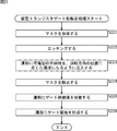
次に、図14のフローチャートを参照して、図13の例の縦型トランジスタ製造部231により実行される縦型トランジスタゲート部製造処理の流れの例を説明する。 <Vertical transistor gate manufacturing process flow>
Next, an example of the flow of the vertical transistor gate part manufacturing process executed by the verticaltransistor manufacturing part 231 of the example of FIG. 13 will be described with reference to the flowchart of FIG.
次に、図14のフローチャートを参照して、図13の例の縦型トランジスタ製造部231により実行される縦型トランジスタゲート部製造処理の流れの例を説明する。 <Vertical transistor gate manufacturing process flow>
Next, an example of the flow of the vertical transistor gate part manufacturing process executed by the vertical
縦型トランジスタゲート部製造処理が開始されると、マスク形成部241は、ステップS101において、半導体基板111の表面側から、転送トランジスタ120のゲート部を形成する位置(例えば、光電変換部112の表面側)に、溝部を形成するためのマスクを形成する。
When the vertical transistor gate part manufacturing process is started, the mask forming part 241 forms the position (for example, the surface of the photoelectric conversion part 112) where the gate part of the transfer transistor 120 is formed from the surface side of the semiconductor substrate 111 in step S101. A mask for forming a groove is formed on the side.
ステップS102において、エッチング部242は、ステップS101において形成されたそのマスクに従って、半導体基板111をエッチングして溝部を形成する。
In step S102, the etching unit 242 etches the semiconductor substrate 111 according to the mask formed in step S101 to form a groove.
ステップS103において、導電型不純物注入部243は、半導体基板111の、ステップS102において形成された溝部に導電型の不純物を注入する。
In step S103, the conductive impurity implantation portion 243 implants a conductive impurity into the groove formed in step S102 of the semiconductor substrate 111.
ステップS104において、マスク除去部244は、ステップS101において形成されたマスクを除去する。
In step S104, the mask removing unit 244 removes the mask formed in step S101.
ゲート絶縁膜被着部245とゲート絶縁膜加工部246は、ステップS102において形成された溝部をその深さ方向に複数階層化し、最も深い階層から最も浅い階層に向かう順で、階層毎に処理を行う。
The gate insulating film deposition part 245 and the gate insulating film processing part 246 divide the groove formed in step S102 into a plurality of layers in the depth direction, and perform processing for each layer in order from the deepest layer to the shallowest layer. Do.
つまり、ステップS105において、ゲート絶縁膜被着部245は、ステップS102において形成された溝部の処理対象の階層(つまり、溝部の処理対象の深さの範囲)に対して、ゲート絶縁膜122をその階層に応じた膜厚で被着する。例えば、1回目の処理であれば、ゲート絶縁膜被着部245は、最も深い階層(すなわち、溝部の底辺から所定の深さまでの範囲)に対して、ゲート絶縁膜122を、その階層に応じた所定の膜厚となるように被着する。また、2回目の処理であれば、ゲート絶縁膜被着部245は、その次の階層(その次の深さの範囲)に対して、ゲート絶縁膜122の被着を行う。
That is, in step S105, the gate insulating film deposition portion 245 applies the gate insulating film 122 to the layer to be processed in the groove formed in step S102 (that is, the depth range of the groove to be processed). Deposit with a film thickness according to the layer. For example, in the case of the first treatment, the gate insulating film deposition portion 245 has the gate insulating film 122 corresponding to the deepest layer (that is, the range from the bottom of the trench to a predetermined depth) according to the layer. The film is deposited to have a predetermined film thickness. In the second process, the gate insulating film deposition portion 245 deposits the gate insulating film 122 on the next layer (the next depth range).
ステップS106において、ゲート絶縁膜被着部245は、全ての階層のゲート絶縁膜122を形成したか否かを判定する。ゲート絶縁膜122が形成されていない階層が存在すると判定された場合、処理はステップS107に進む。
In step S106, the gate insulating film deposition part 245 determines whether or not the gate insulating films 122 of all the layers have been formed. If it is determined that there is a hierarchy in which the gate insulating film 122 is not formed, the process proceeds to step S107.
ステップS107において、ゲート絶縁膜加工部246は、ステップS106において被着されたゲート絶縁膜122を、処理対象の階層に応じた所定の深さまで除去する。つまり、ゲート絶縁膜加工部246は、ステップS106において、溝部の、処理対象の階層の深さの下限(最浅部)よりも浅い部分に被着したゲート絶縁膜122を除去する。これにより、溝部の、最深部(底辺)から、処理対象の階層の最浅部までのゲート絶縁膜122の被着が終了する。
In step S107, the gate insulating film processing unit 246 removes the gate insulating film 122 deposited in step S106 to a predetermined depth corresponding to the layer to be processed. That is, in step S106, the gate insulating film processing unit 246 removes the gate insulating film 122 deposited on a portion of the trench that is shallower than the lower limit (the shallowest portion) of the depth of the layer to be processed. This completes the deposition of the gate insulating film 122 from the deepest part (bottom side) of the trench to the shallowest part of the layer to be processed.
ステップS107の処理が終了すると、処理はステップS105に戻る。つまり、ステップS105乃至ステップS107の各処理が階層毎に繰り返し実行される。そして、全ての階層について処理が行われ、ステップS106において、全ての階層のゲート絶縁膜122が形成されたと判定された場合、処理はステップS108に進む。
When the process in step S107 is completed, the process returns to step S105. That is, each process of step S105 to step S107 is repeatedly executed for each hierarchy. Then, the process is performed for all the layers, and if it is determined in step S106 that the gate insulating film 122 of all the layers has been formed, the process proceeds to step S108.
このようにすることにより、図5や図7の例のように、溝部の深さ方向に、すなわち、電荷転送方向に、膜厚が階段状に変化するようにゲート絶縁膜122が形成される。
By doing so, the gate insulating film 122 is formed so that the film thickness changes stepwise in the depth direction of the groove, that is, in the charge transfer direction, as in the examples of FIGS. .
ステップS108において、ゲート電極形成部247は、以上のように形成されたゲート絶縁膜122の溝部にゲート電極123を形成する。
In step S108, the gate electrode formation portion 247 forms the gate electrode 123 in the groove portion of the gate insulating film 122 formed as described above.
ステップS108の処理が終了すると、縦型トランジスタゲート部製造処理が終了する。
When the processing in step S108 is completed, the vertical transistor gate manufacturing process is completed.
以上のように処理を行うことにより、縦型トランジスタ製造部231は、例えば、図5や図7を参照して説明した例のような転送トランジスタ120のゲート部を製造することができる。つまり、イメージセンサ製造部202は、図5や図7を参照して説明した例のような転送トランジスタ120を有するイメージセンサ100を製造することができる。
By performing the processing as described above, the vertical transistor manufacturing unit 231 can manufacture the gate portion of the transfer transistor 120 as in the example described with reference to FIGS. 5 and 7, for example. That is, the image sensor manufacturing unit 202 can manufacture the image sensor 100 including the transfer transistor 120 as in the example described with reference to FIGS. 5 and 7.
<縦型トランジスタゲート部製造処理の流れ>
次に、図15のフローチャートを参照して、図13の例の縦型トランジスタ製造部231により実行される縦型トランジスタゲート部製造処理の流れの他の例を説明する。 <Vertical transistor gate manufacturing process flow>
Next, another example of the flow of the vertical transistor gate part manufacturing process executed by the verticaltransistor manufacturing part 231 of the example of FIG. 13 will be described with reference to the flowchart of FIG.
次に、図15のフローチャートを参照して、図13の例の縦型トランジスタ製造部231により実行される縦型トランジスタゲート部製造処理の流れの他の例を説明する。 <Vertical transistor gate manufacturing process flow>
Next, another example of the flow of the vertical transistor gate part manufacturing process executed by the vertical
この場合、縦型トランジスタゲート部製造処理が開始されると、マスク形成部241は、ステップS121において、図14の場合と同様にマスクを形成する。
In this case, when the vertical transistor gate part manufacturing process is started, the mask forming part 241 forms a mask in the same manner as in FIG. 14 in step S121.
ステップS122において、エッチング部242は、図14の場合と同様に半導体基板111をエッチングして溝部を形成する。
In step S122, the etching unit 242 etches the semiconductor substrate 111 to form a groove as in the case of FIG.
ステップS123において、導電型不純物注入部243は、図14の場合と同様に導電型の不純物を溝部に注入する。
In step S123, the conductivity type impurity implantation section 243 implants conductivity type impurities into the groove portion as in the case of FIG.
ステップS124において、マスク除去部244は、図14の場合と同様にマスクを除去する。
In step S124, the mask removing unit 244 removes the mask as in the case of FIG.
ステップS125において、ゲート絶縁膜被着部245は、ステップS122において形成された溝部にゲート絶縁膜122を所定の膜厚で被着する。溝部を埋めるようにゲート絶縁膜122を被着してもよい。
In step S125, the gate insulating film deposition portion 245 deposits the gate insulating film 122 with a predetermined film thickness on the trench formed in step S122. The gate insulating film 122 may be deposited so as to fill the trench.
ステップS126において、ゲート絶縁膜加工部246は、ステップS125において被着されたゲート絶縁膜122を加工して、メサ型の溝を形成する。
In step S126, the gate insulating film processing unit 246 processes the gate insulating film 122 deposited in step S125 to form a mesa groove.
ステップS127において、ゲート電極形成部247は、以上のように形成されたゲート絶縁膜122のメサ型の溝部にゲート電極123を形成する。
In step S127, the gate electrode forming portion 247 forms the gate electrode 123 in the mesa-type groove portion of the gate insulating film 122 formed as described above.
ステップS127の処理が終了すると、縦型トランジスタゲート部製造処理が終了する。
When the processing in step S127 is completed, the vertical transistor gate manufacturing process is completed.
以上のように処理を行うことにより、縦型トランジスタ製造部231は、例えば、図4や図6を参照して説明した例のように、ゲート絶縁膜122の膜厚が電荷転送方向に漸次変化するような転送トランジスタ120のゲート部を製造することができる。つまり、イメージセンサ製造部202は、図4や図6を参照して説明した例のような転送トランジスタ120を有するイメージセンサ100を製造することができる。
By performing the processing as described above, the vertical transistor manufacturing unit 231 gradually changes the film thickness of the gate insulating film 122 in the charge transfer direction as in the example described with reference to FIGS. Thus, the gate portion of the transfer transistor 120 can be manufactured. That is, the image sensor manufacturing unit 202 can manufacture the image sensor 100 including the transfer transistor 120 as in the example described with reference to FIGS. 4 and 6.
<縦型トランジスタ製造部>
図16は、縦型トランジスタ製造部231が有する転送トランジスタ120のゲート部の製造に関する処理を行う主な処理部の他の構成例を示すブロック図である。 <Vertical transistor manufacturing department>
FIG. 16 is a block diagram illustrating another configuration example of a main processing unit that performs processing related to the manufacture of the gate portion of thetransfer transistor 120 included in the vertical transistor manufacturing unit 231.
図16は、縦型トランジスタ製造部231が有する転送トランジスタ120のゲート部の製造に関する処理を行う主な処理部の他の構成例を示すブロック図である。 <Vertical transistor manufacturing department>
FIG. 16 is a block diagram illustrating another configuration example of a main processing unit that performs processing related to the manufacture of the gate portion of the
図16に示されるように、この場合、縦型トランジスタ製造部231は、マスク形成部241、エッチング部242、導電型不純物注入部243、非導電型不純物注入部251、マスク除去部244、ゲート絶縁膜被着部245、およびゲート電極形成部247を有する。
As shown in FIG. 16, in this case, the vertical transistor manufacturing unit 231 includes a mask forming unit 241, an etching unit 242, a conductive impurity implantation unit 243, a non-conductive impurity implantation unit 251, a mask removal unit 244, and a gate insulation. A film deposition portion 245 and a gate electrode formation portion 247 are included.
非導電型不純物注入部251は、非導電型不純物の注入に関する処理を行う。溝部に、非導電型不純物を注入することにより、増速酸化による酸化膜(つまり、ゲート絶縁膜122)の膜厚制御を行うことができる。つまり、非導電型不純物注入部251は、溝部に注入する非導電型不純物の注入量(濃度)を制御することによって、ゲート絶縁膜122の膜厚を制御することができる。すなわち、非導電型不純物注入部251は、溝部の深さ方向に応じて、非導電型不純物の注入量(濃度)を制御することによって、ゲート絶縁膜122の膜厚(つまり、電荷転送チャネルのポテンシャルの深さ)を溝部の深さ方向に(つまり、電荷転送方向に)制御することができる。
The non-conductive type impurity implantation unit 251 performs a process related to the implantation of non-conductive type impurities. By implanting a non-conductive impurity into the trench, the film thickness of the oxide film (that is, the gate insulating film 122) can be controlled by accelerated oxidation. That is, the non-conductive impurity implantation portion 251 can control the thickness of the gate insulating film 122 by controlling the injection amount (concentration) of the non-conductive impurity implanted into the trench. That is, the non-conductive impurity implantation portion 251 controls the film thickness of the gate insulating film 122 (that is, the charge transfer channel) by controlling the implantation amount (concentration) of the non-conductive impurity in accordance with the depth direction of the groove. (Potential depth) can be controlled in the depth direction of the groove (that is, in the charge transfer direction).
したがって、このような構成とすることにより、縦型トランジスタ製造部231は、例えば、図4乃至図7を参照して説明した各例のゲート部を製造することができる。つまり、イメージセンサ製造部202は、図4乃至図7を参照して説明した各例のような転送トランジスタ120を有するイメージセンサ100を製造することができる。
Therefore, with such a configuration, the vertical transistor manufacturing unit 231 can manufacture, for example, the gate portions of the examples described with reference to FIGS. That is, the image sensor manufacturing unit 202 can manufacture the image sensor 100 including the transfer transistor 120 as in each example described with reference to FIGS.
<縦型トランジスタゲート部製造処理の流れ>
次に、図17のフローチャートを参照して、図16の例の縦型トランジスタ製造部231により実行される縦型トランジスタゲート部製造処理の流れの他の例を説明する。 <Vertical transistor gate manufacturing process flow>
Next, another example of the flow of the vertical transistor gate part manufacturing process executed by the verticaltransistor manufacturing part 231 of the example of FIG. 16 will be described with reference to the flowchart of FIG.
次に、図17のフローチャートを参照して、図16の例の縦型トランジスタ製造部231により実行される縦型トランジスタゲート部製造処理の流れの他の例を説明する。 <Vertical transistor gate manufacturing process flow>
Next, another example of the flow of the vertical transistor gate part manufacturing process executed by the vertical
この場合、縦型トランジスタゲート部製造処理が開始されると、マスク形成部241乃至導電型不純物注入部243は、ステップS141乃至ステップS143の各処理を、図14のステップS101乃至ステップS103の各処理と同様に実行する。
In this case, when the vertical transistor gate part manufacturing process is started, the mask formation part 241 to the conductive impurity implantation part 243 perform the processes in steps S141 to S143 and the processes in steps S101 to S103 in FIG. Run in the same way as
ステップS144において、非導電型不純物注入部251は、ステップS142において形成された溝部の底面や側面に非導電型の不純物を、その深さに応じた濃度で注入する。
In step S144, the non-conductive impurity implantation portion 251 implants a non-conductive impurity at a concentration corresponding to the depth of the bottom surface or side surface of the groove formed in step S142.
ステップS145において、マスク除去部244は、図14の場合と同様にマスクを除去する。
In step S145, the mask removing unit 244 removes the mask as in the case of FIG.
ステップS146において、ゲート絶縁膜被着部245は、ステップS142において形成された溝部にゲート絶縁膜122を所定の膜厚で被着する。ステップS144の処理により、溝部には、非導電型不純物が適宜注入されるので、増速酸化によりゲート絶縁膜122が、その非導電型不純物の濃度に応じた膜厚となる。つまり、ゲート絶縁膜122は、溝部の深さに応じた膜厚となる。
In step S146, the gate insulating film depositing portion 245 deposits the gate insulating film 122 with a predetermined film thickness in the trench formed in step S142. By the processing in step S144, non-conductive impurities are appropriately implanted into the trench, so that the gate insulating film 122 has a thickness corresponding to the concentration of the non-conductive impurities by accelerated oxidation. That is, the gate insulating film 122 has a thickness corresponding to the depth of the groove.
ステップS147において、ゲート電極形成部247は、以上のように形成されたゲート絶縁膜122の溝部にゲート電極123を形成する。
In step S147, the gate electrode formation portion 247 forms the gate electrode 123 in the groove portion of the gate insulating film 122 formed as described above.
ステップS147の処理が終了すると、縦型トランジスタゲート部製造処理が終了する。
When the processing in step S147 is completed, the vertical transistor gate manufacturing process is completed.
以上のように処理を行うことにより、縦型トランジスタ製造部231は、例えば、図4乃至図7を参照して説明した各例の転送トランジスタ120のゲート部を製造することができる。
By performing the processing as described above, the vertical transistor manufacturing unit 231 can manufacture, for example, the gate portion of the transfer transistor 120 in each example described with reference to FIGS.
例えば、ステップS144において、非導電型不純物注入部251が、非導電型の不純物を、その濃度を溝部の深さ方向に階段状に変化させて注入することにより、ステップS146の処理により形成されるゲート絶縁膜122の膜厚が深さ方向に階段状に変化するようになるので、縦型トランジスタ製造部231は、例えば、図5や図7を参照して説明した各例の転送トランジスタ120のゲート部を製造することができる。
For example, in step S144, the non-conductive impurity implantation part 251 is formed by the process of step S146 by injecting the non-conductive impurity while changing its concentration stepwise in the depth direction of the groove. Since the film thickness of the gate insulating film 122 changes stepwise in the depth direction, the vertical transistor manufacturing unit 231 has, for example, the transfer transistor 120 of each example described with reference to FIGS. A gate part can be manufactured.
また、例えば、ステップS144において、非導電型不純物注入部251が、非導電型の不純物を、その濃度を溝部の深さ方向に漸次変化させて注入することにより、ステップS146の処理により形成されるゲート絶縁膜122の膜厚が深さ方向に漸次変化するようになるので、縦型トランジスタ製造部231は、例えば、図4や図6を参照して説明した各例の転送トランジスタ120のゲート部を製造することができる。
In addition, for example, in step S144, the non-conductive impurity implantation part 251 is formed by the process of step S146 by injecting non-conductive impurities by gradually changing the concentration thereof in the depth direction of the groove. Since the thickness of the gate insulating film 122 gradually changes in the depth direction, the vertical transistor manufacturing unit 231 includes, for example, the gate portion of the transfer transistor 120 in each example described with reference to FIGS. 4 and 6. Can be manufactured.
つまり、イメージセンサ製造部202は、図4乃至図7を参照して説明した例のような転送トランジスタ120を有するイメージセンサ100を製造することができる。
That is, the image sensor manufacturing unit 202 can manufacture the image sensor 100 including the transfer transistor 120 as in the example described with reference to FIGS.
<縦型トランジスタ製造部>
図18は、縦型トランジスタ製造部231が有する転送トランジスタ120のゲート部の製造に関する処理を行う主な処理部のさらに他の構成例を示すブロック図である。 <Vertical transistor manufacturing department>
FIG. 18 is a block diagram showing still another configuration example of a main processing unit that performs processing related to manufacturing of the gate portion of thetransfer transistor 120 included in the vertical transistor manufacturing unit 231.
図18は、縦型トランジスタ製造部231が有する転送トランジスタ120のゲート部の製造に関する処理を行う主な処理部のさらに他の構成例を示すブロック図である。 <Vertical transistor manufacturing department>
FIG. 18 is a block diagram showing still another configuration example of a main processing unit that performs processing related to manufacturing of the gate portion of the
図18に示されるように、この場合、縦型トランジスタ製造部231は、マスク形成部241、エッチング部242、導電型不純物注入部243、マスク除去部244、ゲート絶縁膜被着部245、およびゲート電極形成部247を有する。
As shown in FIG. 18, in this case, the vertical transistor manufacturing unit 231 includes a mask forming unit 241, an etching unit 242, a conductive impurity implantation unit 243, a mask removing unit 244, a gate insulating film deposition unit 245, and a gate. An electrode formation portion 247 is included.
導電型不純物注入部243は、導電型不純物を、溝部の注入する位置の深さに応じた濃度で注入する。導電型不純物の濃度を、注入する深さに応じて制御することにより、導電型不純物注入部243は、電荷転送チャネル121のポテンシャルの深さを溝部の深さ方向に(つまり、電荷転送方向に)制御することができる。つまり、導電型不純物注入部243は、電荷転送チャネル121において、電荷転送方向にポテンシャルの勾配を形成することができる。
The conductivity type impurity implantation part 243 implants the conductivity type impurity at a concentration according to the depth of the position where the groove is implanted. By controlling the concentration of the conductive impurity according to the depth of implantation, the conductive impurity implanted portion 243 allows the potential depth of the charge transfer channel 121 to be in the depth direction of the groove (that is, in the charge transfer direction). ) Can be controlled. That is, the conductivity type impurity implantation part 243 can form a potential gradient in the charge transfer direction in the charge transfer channel 121.
したがって、このような構成とすることにより、縦型トランジスタ製造部231は、例えば、図8を参照して説明した例等のような、電荷転送チャネル121に注入された導電型不純物の濃度が電荷転送方向に変化するゲート部を製造することができる。つまり、イメージセンサ製造部202は、図8を参照して説明した例等のような、電荷転送チャネル121に注入された導電型不純物の濃度が電荷転送方向に変化する転送トランジスタ120を有するイメージセンサ100を製造することができる。
Therefore, with this configuration, the vertical transistor manufacturing unit 231 has the concentration of the conductive impurity injected into the charge transfer channel 121 as in the example described with reference to FIG. A gate portion that changes in the transfer direction can be manufactured. That is, the image sensor manufacturing unit 202 includes the transfer transistor 120 in which the concentration of the conductive impurity injected into the charge transfer channel 121 changes in the charge transfer direction, such as the example described with reference to FIG. 100 can be manufactured.
<縦型トランジスタゲート部製造処理の流れ>
次に、図19のフローチャートを参照して、図18の例の縦型トランジスタ製造部231により実行される縦型トランジスタゲート部製造処理の流れの他の例を説明する。 <Vertical transistor gate manufacturing process flow>
Next, another example of the flow of the vertical transistor gate part manufacturing process executed by the verticaltransistor manufacturing part 231 of the example of FIG. 18 will be described with reference to the flowchart of FIG.
次に、図19のフローチャートを参照して、図18の例の縦型トランジスタ製造部231により実行される縦型トランジスタゲート部製造処理の流れの他の例を説明する。 <Vertical transistor gate manufacturing process flow>
Next, another example of the flow of the vertical transistor gate part manufacturing process executed by the vertical
この場合、縦型トランジスタゲート部製造処理が開始されると、マスク形成部241およびエッチング部242は、ステップS161およびステップS162の各処理を、図14のステップS101およびステップS102の各処理と同様に実行する。
In this case, when the vertical transistor gate manufacturing process is started, the mask forming unit 241 and the etching unit 242 perform the processes in steps S161 and S162 in the same manner as the processes in steps S101 and S102 in FIG. Execute.
ステップS163において、導電型不純物注入部243は、導電型不純物をステップS162において形成された溝部に、その注入する位置の深さに応じた濃度で注入する。
In step S163, the conductivity type impurity implantation part 243 implants the conductivity type impurity into the groove formed in step S162 at a concentration according to the depth of the position where the impurity is implanted.
ステップS164において、マスク除去部244は、図14の場合と同様にマスクを除去する。
In step S164, the mask removing unit 244 removes the mask as in the case of FIG.
ステップS165において、ゲート絶縁膜被着部245は、ステップS162において形成された溝部にゲート絶縁膜122を所定の膜厚で被着する。
In step S165, the gate insulating film deposited portion 245 deposits the gate insulating film 122 with a predetermined film thickness on the groove formed in step S162.
ステップS166において、ゲート電極形成部247は、以上のように形成されたゲート絶縁膜122の溝部にゲート電極123を形成する。
In step S166, the gate electrode forming portion 247 forms the gate electrode 123 in the groove portion of the gate insulating film 122 formed as described above.
ステップS166の処理が終了すると、縦型トランジスタゲート部製造処理が終了する。
When the process in step S166 is completed, the vertical transistor gate manufacturing process is completed.
以上のように処理を行うことにより、縦型トランジスタ製造部231は、例えば図8を参照して説明した例等のような、電荷転送チャネル121に注入された導電型不純物の濃度が電荷転送方向に変化する転送トランジスタ120のゲート部を製造することができる。つまり、イメージセンサ製造部202は、図8を参照して説明した例等のような、電荷転送チャネル121に注入された導電型不純物の濃度が電荷転送方向に変化する転送トランジスタ120を有するイメージセンサ100を製造することができる。
By performing the processing as described above, the vertical transistor manufacturing unit 231 has the concentration of the conductive impurity injected into the charge transfer channel 121 as in the example described with reference to FIG. The gate portion of the transfer transistor 120 that changes to can be manufactured. That is, the image sensor manufacturing unit 202 includes the transfer transistor 120 in which the concentration of the conductive impurity injected into the charge transfer channel 121 changes in the charge transfer direction, such as the example described with reference to FIG. 100 can be manufactured.
<縦型トランジスタ製造部>
次に、電荷転送チャネル121に、ゲート電極123に沿った回転方向にポテンシャルの勾配を形成させる場合の、縦型トランジスタ製造部231の構成例について説明する。この場合、縦型トランジスタ製造部231は、例えば、図13を参照して説明した例と同様の構成を有するようにしてもよい。つまり、縦型トランジスタ製造部231が、マスク形成部241乃至ゲート電極形成部247を有するようにしてもよい。 <Vertical transistor manufacturing department>
Next, a configuration example of the verticaltransistor manufacturing unit 231 in the case where a potential gradient is formed in the charge transfer channel 121 in the rotation direction along the gate electrode 123 will be described. In this case, the vertical transistor manufacturing unit 231 may have the same configuration as the example described with reference to FIG. That is, the vertical transistor manufacturing unit 231 may include the mask formation unit 241 to the gate electrode formation unit 247.
次に、電荷転送チャネル121に、ゲート電極123に沿った回転方向にポテンシャルの勾配を形成させる場合の、縦型トランジスタ製造部231の構成例について説明する。この場合、縦型トランジスタ製造部231は、例えば、図13を参照して説明した例と同様の構成を有するようにしてもよい。つまり、縦型トランジスタ製造部231が、マスク形成部241乃至ゲート電極形成部247を有するようにしてもよい。 <Vertical transistor manufacturing department>
Next, a configuration example of the vertical
<縦型トランジスタゲート部製造処理の流れ>
次に、図20のフローチャートを参照して、この場合の縦型トランジスタ製造部231により実行される縦型トランジスタゲート部製造処理の流れの例を説明する。 <Vertical transistor gate manufacturing process flow>
Next, an example of the flow of the vertical transistor gate part manufacturing process executed by the verticaltransistor manufacturing part 231 in this case will be described with reference to the flowchart of FIG.
次に、図20のフローチャートを参照して、この場合の縦型トランジスタ製造部231により実行される縦型トランジスタゲート部製造処理の流れの例を説明する。 <Vertical transistor gate manufacturing process flow>
Next, an example of the flow of the vertical transistor gate part manufacturing process executed by the vertical
この場合、縦型トランジスタゲート部製造処理が開始されると、マスク形成部241乃至ゲート絶縁膜被着部245は、ステップS201乃至ステップS205の各処理を、図15のステップS121乃至ステップS125の各処理と同様に実行する。
In this case, when the vertical transistor gate part manufacturing process is started, the mask forming part 241 to the gate insulating film deposition part 245 perform the processes in steps S201 to S205 and the processes in steps S121 to S125 in FIG. Execute in the same way as the processing.
ステップS206において、ゲート絶縁膜加工部246は、ステップS205において被着されたゲート絶縁膜122を加工して、ゲート絶縁膜122が回転方向の位置に応じた膜厚になるように、ゲート絶縁膜122に溝部を形成する。例えばゲート絶縁膜加工部246は、図11のAや図11のBの例のようにして、ゲート絶縁膜122に溝部を形成することにより、ゲート絶縁膜122の膜厚を回転方向の位置に応じて変化させることができる。
In step S206, the gate insulating film processing unit 246 processes the gate insulating film 122 deposited in step S205 so that the gate insulating film 122 has a thickness corresponding to the position in the rotation direction. A groove is formed in 122. For example, the gate insulating film processing portion 246 forms the groove portion in the gate insulating film 122 as in the example of FIG. 11A or FIG. It can be changed accordingly.
ステップS207において、ゲート電極形成部247は、ステップS206において形成されたゲート絶縁膜122の溝部にゲート電極123を形成する。
In step S207, the gate electrode formation portion 247 forms the gate electrode 123 in the groove portion of the gate insulating film 122 formed in step S206.
ステップS207の処理が終了すると、縦型トランジスタゲート部製造処理が終了する。
When the process in step S207 is completed, the vertical transistor gate manufacturing process is completed.
以上のように処理を行うことにより、縦型トランジスタ製造部231は、例えば、図10や図11を参照して説明した例のように、ゲート絶縁膜122の膜厚が回転方向に漸次若しくは階段状に変化するような転送トランジスタ120のゲート部を製造することができる。つまり、イメージセンサ製造部202は、図10や図11を参照して説明した例のような転送トランジスタ120を有するイメージセンサ100を製造することができる。
By performing the processing as described above, the vertical transistor manufacturing unit 231 causes the film thickness of the gate insulating film 122 to gradually or stepwise in the rotation direction as in the example described with reference to FIGS. A gate portion of the transfer transistor 120 that changes in a shape can be manufactured. That is, the image sensor manufacturing unit 202 can manufacture the image sensor 100 including the transfer transistor 120 as in the example described with reference to FIGS. 10 and 11.
<縦型トランジスタ製造部>
次に、電荷転送チャネル121に、ゲート電極123に沿った回転方向にポテンシャルの勾配を形成させる場合の、縦型トランジスタ製造部231の他の構成例について説明する。この場合、縦型トランジスタ製造部231は、例えば、図18を参照して説明した例と同様の構成を有するようにしてもよい。つまり、縦型トランジスタ製造部231が、マスク形成部241乃至ゲート絶縁膜被着部245、並びに、ゲート電極形成部247を有するようにしてもよい。 <Vertical transistor manufacturing department>
Next, another configuration example of the verticaltransistor manufacturing unit 231 in the case where a potential gradient is formed in the charge transfer channel 121 in the rotation direction along the gate electrode 123 will be described. In this case, the vertical transistor manufacturing unit 231 may have the same configuration as the example described with reference to FIG. That is, the vertical transistor manufacturing unit 231 may include the mask formation unit 241 to the gate insulating film deposition unit 245 and the gate electrode formation unit 247.
次に、電荷転送チャネル121に、ゲート電極123に沿った回転方向にポテンシャルの勾配を形成させる場合の、縦型トランジスタ製造部231の他の構成例について説明する。この場合、縦型トランジスタ製造部231は、例えば、図18を参照して説明した例と同様の構成を有するようにしてもよい。つまり、縦型トランジスタ製造部231が、マスク形成部241乃至ゲート絶縁膜被着部245、並びに、ゲート電極形成部247を有するようにしてもよい。 <Vertical transistor manufacturing department>
Next, another configuration example of the vertical
<縦型トランジスタゲート部製造処理の流れ>
次に、図21のフローチャートを参照して、この場合の縦型トランジスタ製造部231により実行される縦型トランジスタゲート部製造処理の流れの例を説明する。 <Vertical transistor gate manufacturing process flow>
Next, an example of the flow of the vertical transistor gate part manufacturing process executed by the verticaltransistor manufacturing part 231 in this case will be described with reference to the flowchart of FIG.
次に、図21のフローチャートを参照して、この場合の縦型トランジスタ製造部231により実行される縦型トランジスタゲート部製造処理の流れの例を説明する。 <Vertical transistor gate manufacturing process flow>
Next, an example of the flow of the vertical transistor gate part manufacturing process executed by the vertical
この場合、縦型トランジスタゲート部製造処理が開始されると、マスク形成部241およびエッチング部242は、ステップS221およびステップS222の各処理を、図19のステップS161およびステップS162の各処理と同様に実行する。
In this case, when the vertical transistor gate manufacturing process is started, the mask forming unit 241 and the etching unit 242 perform the processes in steps S221 and S222 in the same manner as the processes in steps S161 and S162 in FIG. Execute.
ステップS223において、導電型不純物注入部243は、導電型不純物を、ステップS222において形成された溝部に、その注入する回転方向の位置に応じた濃度で注入する。
In step S223, the conductivity type impurity implantation unit 243 implants the conductivity type impurity into the groove formed in step S222 at a concentration according to the position in the rotational direction of the implantation.
マスク除去部244、ゲート絶縁膜被着部245、およびゲート電極形成部247は、ステップS224乃至ステップS226の各処理を、図19のステップS164乃至ステップS166の各処理と同様に実行する。
The mask removal unit 244, the gate insulating film deposition unit 245, and the gate electrode formation unit 247 execute the processes in steps S224 to S226 in the same manner as the processes in steps S164 to S166 in FIG.
ステップS226の処理が終了すると、縦型トランジスタゲート部製造処理が終了する。
When the processing in step S226 is completed, the vertical transistor gate manufacturing process is completed.
以上のように処理を行うことにより、縦型トランジスタ製造部231は、例えば図10や図11のCを参照して説明した例等のような、電荷転送チャネル121に注入された導電型不純物の濃度が回転方向に変化する転送トランジスタ120のゲート部を製造することができる。つまり、イメージセンサ製造部202は、図10や図11のCを参照して説明した例等のような、電荷転送チャネル121に注入された導電型不純物の濃度が回転方向に変化する転送トランジスタ120を有するイメージセンサ100を製造することができる。
By performing the processing as described above, the vertical transistor manufacturing unit 231 can remove the conductive impurities injected into the charge transfer channel 121 such as the example described with reference to FIG. The gate portion of the transfer transistor 120 whose concentration changes in the rotation direction can be manufactured. That is, the image sensor manufacturing unit 202 transfers the transfer transistor 120 in which the concentration of the conductive impurity injected into the charge transfer channel 121 changes in the rotation direction, such as the example described with reference to FIGS. 10 and 11C. Can be manufactured.
<3.第3の実施の形態>
<撮像装置>
以上に説明した、本技術を適用して製造したイメージセンサ100(撮像素子)は、例えば撮像装置等のデバイスに適用することができる。すなわち、本技術は、撮像素子としてだけでなく、その撮像素子を用いたデバイス(例えば、撮像装置等)として実施することもできる。 <3. Third Embodiment>
<Imaging device>
The image sensor 100 (image pickup device) manufactured by applying the present technology described above can be applied to a device such as an image pickup apparatus, for example. That is, the present technology can be implemented not only as an image sensor, but also as a device (for example, an image pickup apparatus) using the image sensor.
図22は、本技術を適用した電子機器の一例としての撮像装置の主な構成例を示すブロック図である。図22に示される撮像装置600は、被写体を撮像し、その被写体の画像を電気信号として出力する装置である。
FIG. 22 is a block diagram illustrating a main configuration example of an imaging apparatus as an example of an electronic apparatus to which the present technology is applied. An imaging apparatus 600 shown in FIG. 22 is an apparatus that images a subject and outputs an image of the subject as an electrical signal.
図22に示されるように撮像装置600は、光学部611、CMOSセンサ612、A/D変換器613、操作部614、制御部615、画像処理部616、表示部617、コーデック処理部618、および記録部619を有する。
As shown in FIG. 22, the imaging apparatus 600 includes an optical unit 611, a CMOS sensor 612, an A / D converter 613, an operation unit 614, a control unit 615, an image processing unit 616, a display unit 617, a codec processing unit 618, and A recording unit 619 is included.
光学部611は、被写体までの焦点を調整し、焦点が合った位置からの光を集光するレンズ、露出を調整する絞り、および、撮像のタイミングを制御するシャッタ等よりなる。光学部611は、被写体からの光(入射光)を透過し、CMOSセンサ612に供給する。
The optical unit 611 includes a lens that adjusts the focal point to the subject and collects light from the focused position, an aperture that adjusts exposure, a shutter that controls the timing of imaging, and the like. The optical unit 611 transmits light (incident light) from the subject and supplies the light to the CMOS sensor 612.
CMOSセンサ612は、入射光を光電変換して画素毎の信号(画素信号)をA/D変換器613に供給する。
The CMOS sensor 612 photoelectrically converts incident light and supplies a signal (pixel signal) for each pixel to the A / D converter 613.
A/D変換器613は、CMOSセンサ612から、所定のタイミングで供給された画素信号を、デジタルデータ(画像データ)に変換し、所定のタイミングで順次、画像処理部616に供給する。
The A / D converter 613 converts the pixel signal supplied from the CMOS sensor 612 at a predetermined timing into digital data (image data), and sequentially supplies it to the image processing unit 616 at the predetermined timing.
操作部614は、例えば、ジョグダイヤル(商標)、キー、ボタン、またはタッチパネル等の任意の入力デバイスにより構成され、例えばユーザによる操作入力を受け、その操作入力に対応する信号を制御部615に供給する。
The operation unit 614 includes, for example, an arbitrary input device such as a jog dial (trademark), a key, a button, or a touch panel. For example, the operation unit 614 receives an operation input by a user and supplies a signal corresponding to the operation input to the control unit 615. .
制御部615は、操作部614により入力されたユーザの操作入力に対応する信号に基づいて、光学部611、CMOSセンサ612、A/D変換器613、画像処理部616、表示部617、コーデック処理部618、および記録部619の駆動を制御し、各部に撮像に関する処理を行わせる。
The control unit 615 is based on a signal corresponding to the user's operation input input by the operation unit 614, the optical unit 611, the CMOS sensor 612, the A / D converter 613, the image processing unit 616, the display unit 617, and codec processing. The driving of the unit 618 and the recording unit 619 is controlled to cause each unit to perform processing related to imaging.
画像処理部616は、A/D変換器613から供給された画像データに対して、例えば、混色補正や、黒レベル補正、ホワイトバランス調整、デモザイク処理、マトリックス処理、ガンマ補正、およびYC変換等の各種画像処理を施す。画像処理部616は、画像処理を施した画像データを表示部617およびコーデック処理部618に供給する。
The image processing unit 616 performs, for example, color mixture correction, black level correction, white balance adjustment, demosaic processing, matrix processing, gamma correction, and YC conversion on the image data supplied from the A / D converter 613. Various image processing is performed. The image processing unit 616 supplies the image data subjected to the image processing to the display unit 617 and the codec processing unit 618.
表示部617は、例えば、液晶ディスプレイ等として構成され、画像処理部616から供給された画像データに基づいて、被写体の画像を表示する。
The display unit 617 is configured as a liquid crystal display, for example, and displays an image of the subject based on the image data supplied from the image processing unit 616.
コーデック処理部618は、画像処理部616から供給された画像データに対して、所定の方式の符号化処理を施し、得られた符号化データを記録部619に供給する。
The codec processing unit 618 performs a predetermined encoding process on the image data supplied from the image processing unit 616, and supplies the obtained encoded data to the recording unit 619.
記録部619は、コーデック処理部618からの符号化データを記録する。記録部619に記録された符号化データは、必要に応じて画像処理部616に読み出されて復号される。復号処理により得られた画像データは、表示部617に供給され、対応する画像が表示される。
The recording unit 619 records the encoded data from the codec processing unit 618. The encoded data recorded in the recording unit 619 is read out and decoded by the image processing unit 616 as necessary. The image data obtained by the decoding process is supplied to the display unit 617, and a corresponding image is displayed.
以上のような撮像装置600のCMOSセンサ612に上述した本技術を適用する。すなわち、CMOSセンサ612には、本技術を適用したイメージセンサ100が用いられる。したがって、CMOSセンサ612は、光電変換部の電荷を転送する電荷転送チャネルの少なくとも一部においてポテンシャルが勾配を有する縦型トランジスタを備える。したがって、CMOSセンサ612は、電荷をより転送しやすくすることができる。したがって撮像装置600は、被写体を撮像することにより、より高画質な画像を得ることができる(撮像画像の画質の低減を抑制することができる)。
The present technology described above is applied to the CMOS sensor 612 of the imaging apparatus 600 as described above. That is, the image sensor 100 to which the present technology is applied is used for the CMOS sensor 612. Therefore, the CMOS sensor 612 includes a vertical transistor having a potential gradient in at least a part of the charge transfer channel that transfers the charge of the photoelectric conversion unit. Therefore, the CMOS sensor 612 can make it easier to transfer charges. Therefore, the imaging apparatus 600 can obtain a higher quality image by imaging the subject (a reduction in the quality of the captured image can be suppressed).
なお、本技術を適用した撮像装置は、上述した構成に限らず、他の構成であってもよい。例えば、デジタルスチルカメラやビデオカメラだけでなく、携帯電話機、スマートホン、タブレット型デバイス、パーソナルコンピュータ等の、撮像機能を有する情報処理装置であってもよい。また、他の情報処理装置に装着して使用される(若しくは組み込みデバイスとして搭載される)カメラモジュールであってもよい。
Note that the imaging apparatus to which the present technology is applied is not limited to the configuration described above, and may have another configuration. For example, not only a digital still camera and a video camera but also an information processing apparatus having an imaging function, such as a mobile phone, a smart phone, a tablet device, and a personal computer. Further, it may be a camera module used by being mounted on another information processing apparatus (or mounted as an embedded device).
<4.応用例>
<ソフトウェア>
上述した一連の処理は、ハードウェアにより実行させることもできるし、ソフトウェアにより実行させることもできる。上述した一連の処理をソフトウェアにより実行させる場合には、そのソフトウェアを構成するプログラムが、ネットワークや記録媒体からインストールされる。 <4. Application example>
<Software>
The series of processes described above can be executed by hardware or can be executed by software. When the above-described series of processing is executed by software, a program constituting the software is installed from a network or a recording medium.
この記録媒体は、例えば、図12に示されるように、装置本体とは別に、ユーザにプログラムを配信するために配布される、プログラムが記録されているリムーバブルメディア221により構成される。このリムーバブルメディア221には、磁気ディスク(フレキシブルディスクを含む)や光ディスク(CD-ROMやDVDを含む)が含まれる。さらに、光磁気ディスク(MD(Mini Disc)を含む)や半導体メモリ等も含まれる。その場合、例えば、リムーバブルメディア221をドライブ215に装着することにより、そのリムーバブルメディア221に記憶されているこのプログラムを読み出させ、記憶部213にインストールさせることができる。
For example, as shown in FIG. 12, this recording medium includes a removable medium 221 on which a program is recorded, which is distributed to distribute the program to the user, separately from the apparatus main body. The removable medium 221 includes a magnetic disk (including a flexible disk) and an optical disk (including a CD-ROM and a DVD). Further, magneto-optical disks (including MD (Mini-Disc)) and semiconductor memories are also included. In this case, for example, by installing the removable medium 221 in the drive 215, the program stored in the removable medium 221 can be read and installed in the storage unit 213.
また、このプログラムは、ローカルエリアネットワーク、インターネット、デジタル衛星放送といった、有線または無線の伝送媒体を介して提供することもできる。その場合、例えば、プログラムは、通信部214で受信し、記憶部213にインストールすることができる。
This program can also be provided via a wired or wireless transmission medium such as a local area network, the Internet, or digital satellite broadcasting. In this case, for example, the program can be received by the communication unit 214 and installed in the storage unit 213.
その他、このプログラムは、記憶部やROM等に、あらかじめインストールしておくこともできる。例えば、プログラムは、記憶部213や制御部201に内蔵されるROM等に、あらかじめインストールしておくこともできる。
In addition, this program can also be installed in advance in a storage unit or ROM. For example, the program can be installed in advance in a ROM or the like built in the storage unit 213 or the control unit 201.
なお、コンピュータが実行するプログラムは、本明細書で説明する順序に沿って時系列に処理が行われるプログラムであっても良いし、並列に、あるいは呼び出しが行われたとき等の必要なタイミングで処理が行われるプログラムであっても良い。
The program executed by the computer may be a program that is processed in time series in the order described in this specification, or in parallel or at a necessary timing such as when a call is made. It may be a program for processing.
また、本明細書において、記録媒体に記録されるプログラムを記述するステップは、記載された順序に沿って時系列的に行われる処理はもちろん、必ずしも時系列的に処理されなくとも、並列的あるいは個別に実行される処理をも含むものである。
Further, in the present specification, the step of describing the program recorded on the recording medium is not limited to the processing performed in chronological order according to the described order, but may be performed in parallel or It also includes processes that are executed individually.
また、上述した各ステップの処理は、上述した各装置、若しくは、上述した各装置以外の任意の装置において、実行することができる。その場合、その処理を実行する装置が、上述した、その処理を実行するのに必要な機能(機能ブロック等)を有するようにすればよい。また、処理に必要な情報を、適宜、その装置に伝送するようにすればよい。
Further, the processing of each step described above can be executed in each device described above or any device other than each device described above. In that case, the device that executes the process may have the functions (functional blocks and the like) necessary for executing the process described above. Information necessary for processing may be transmitted to the apparatus as appropriate.
<その他>
また、本明細書において、システムとは、複数の構成要素(装置、モジュール(部品)等)の集合を意味し、全ての構成要素が同一筐体中にあるか否かは問わない。したがって、別個の筐体に収納され、ネットワークを介して接続されている複数の装置、及び、1つの筐体の中に複数のモジュールが収納されている1つの装置は、いずれも、システムである。 <Others>
In this specification, the system means a set of a plurality of components (devices, modules (parts), etc.), and it does not matter whether all the components are in the same housing. Accordingly, a plurality of devices housed in separate housings and connected via a network and a single device housing a plurality of modules in one housing are all systems. .
また、以上において、1つの装置(または処理部)として説明した構成を分割し、複数の装置(または処理部)として構成するようにしてもよい。逆に、以上において複数の装置(または処理部)として説明した構成をまとめて1つの装置(または処理部)として構成されるようにしてもよい。また、各装置(または各処理部)の構成に上述した以外の構成を付加するようにしてももちろんよい。さらに、システム全体としての構成や動作が実質的に同じであれば、ある装置(または処理部)の構成の一部を他の装置(または他の処理部)の構成に含めるようにしてもよい。
Also, in the above, the configuration described as one device (or processing unit) may be divided and configured as a plurality of devices (or processing units). Conversely, the configurations described above as a plurality of devices (or processing units) may be combined into a single device (or processing unit). Of course, a configuration other than that described above may be added to the configuration of each device (or each processing unit). Furthermore, if the configuration and operation of the entire system are substantially the same, a part of the configuration of a certain device (or processing unit) may be included in the configuration of another device (or other processing unit). .
以上、添付図面を参照しながら本開示の好適な実施形態について詳細に説明したが、本開示の技術的範囲はかかる例に限定されない。本開示の技術分野における通常の知識を有する者であれば、請求の範囲に記載された技術的思想の範疇内において、各種の変更例または修正例に想到し得ることは明らかであり、これらについても、当然に本開示の技術的範囲に属するものと了解される。
The preferred embodiments of the present disclosure have been described in detail above with reference to the accompanying drawings, but the technical scope of the present disclosure is not limited to such examples. It is obvious that a person having ordinary knowledge in the technical field of the present disclosure can come up with various changes or modifications within the scope of the technical idea described in the claims. Of course, it is understood that it belongs to the technical scope of the present disclosure.
例えば、本技術は、1つの機能を、ネットワークを介して複数の装置で分担、共同して処理するクラウドコンピューティングの構成をとることができる。
For example, the present technology can take a configuration of cloud computing in which one function is shared by a plurality of devices via a network and is jointly processed.
また、上述のフローチャートで説明した各ステップは、1つの装置で実行する他、複数の装置で分担して実行することができる。
Further, each step described in the above flowchart can be executed by one device or can be shared by a plurality of devices.
さらに、1つのステップに複数の処理が含まれる場合には、その1つのステップに含まれる複数の処理は、1つの装置で実行する他、複数の装置で分担して実行することができる。
Further, when a plurality of processes are included in one step, the plurality of processes included in the one step can be executed by being shared by a plurality of apparatuses in addition to being executed by one apparatus.
また、本技術は、これに限らず、このような装置またはシステムを構成する装置に搭載するあらゆる構成、例えば、システムLSI(Large Scale Integration)等としてのプロセッサ、複数のプロセッサ等を用いるモジュール、複数のモジュール等を用いるユニット、ユニットにさらにその他の機能を付加したセット等(すなわち、装置の一部の構成)として実施することもできる。
In addition, the present technology is not limited to this, and any configuration mounted on such a device or a device constituting the system, for example, a processor as a system LSI (Large Scale Integration), a module using a plurality of processors, a plurality of It is also possible to implement as a unit using other modules, a set obtained by further adding other functions to the unit (that is, a partial configuration of the apparatus), and the like.
なお、本技術は以下のような構成も取ることができる。
(1) 光電変換部の電荷を転送する電荷転送チャネルの少なくとも一部においてポテンシャルが勾配を有する縦型トランジスタ
を備える撮像素子。
(2) 前記ポテンシャルは、前記電荷転送チャネルにおける電荷転送方向に、前記電荷の転送先に向かって深くなる勾配を有する
(1)に記載の撮像素子。
(3) 前記電荷転送チャネルは、第1導電型の半導体に形成される第2導電型の前記光電変換部の電荷を転送する第1導電型の電荷転送チャネルであり、
前記電荷転送チャネルとゲート電極との間に形成されるゲート絶縁膜が、前記電荷の転送先に向かって膜厚が漸次薄くなるように形成される
(2)に記載の撮像素子。
(4) 前記電荷転送チャネルは、第1導電型の半導体に形成される第2導電型の前記光電変換部の電荷を転送する第1導電型の電荷転送チャネルであり、
前記電荷転送チャネルとゲート電極との間に形成されるゲート絶縁膜が、前記電荷の転送先に向かって膜厚が階段状に薄くなるように形成される
(2)に記載の撮像素子。
(5) 前記電荷転送チャネルは、第1導電型の半導体に形成される第2導電型の前記光電変換部の電荷を転送する第1導電型の電荷転送チャネルであり、
前記電荷転送チャネルが、前記電荷の転送先に向かって不純物濃度が薄くなるように形成される
(2)乃至(4)のいずれかに記載の撮像素子。
(6) 前記電荷転送チャネルは、第1導電型の半導体に形成される第2導電型の前記光電変換部の電荷を転送する第2導電型の電荷転送チャネルであり、
前記電荷転送チャネルとゲート電極との間に形成されるゲート絶縁膜が、前記電荷の転送先に向かって膜厚が漸次厚くなるように形成される
(2)に記載の撮像素子。
(7) 前記電荷転送チャネルは、第1導電型の半導体に形成される第2導電型の前記光電変換部の電荷を転送する第2導電型の電荷転送チャネルであり、
前記電荷転送チャネルとゲート電極との間に形成されるゲート絶縁膜が、前記電荷の転送先に向かって膜厚が階段状に厚くなるように形成される
(2)に記載の撮像素子。
(8) 前記電荷転送チャネルは、第1導電型の半導体に形成される第2導電型の前記光電変換部の電荷を転送する第2導電型の電荷転送チャネルであり、
前記電荷転送チャネルが、前記電荷の転送先に向かって不純物濃度が濃くなるように形成される
(2)、(6)、(7)のいずれかに記載の撮像素子。
(9) 前記ポテンシャルは、前記電荷転送チャネルにおけるゲート電極に沿った回転方向に勾配を有する
(1)乃至(8)のいずれかに記載の撮像素子。
(10) 前記電荷転送チャネルと前記ゲート電極との間に形成されるゲート絶縁膜の膜厚が、前記回転方向に変化する
(9)に記載の撮像素子。
(11) 前記電荷転送チャネルの不純物濃度が、前記回転方向に変化する
(9)または(10)に記載の撮像素子。
(12) 光電変換部の電荷を転送する電荷転送チャネルの少なくとも一部においてポテンシャルが勾配を有する縦型トランジスタを備える撮像素子と、
前記撮像素子により得られる撮像画像データを画像処理する画像処理部と
を備える撮像装置。
(13) 撮像素子を製造する製造装置であって、
光電変換部の電荷を転送する電荷転送チャネルの少なくとも一部においてポテンシャルが勾配を有する縦型トランジスタを製造する縦型トランジスタ製造部
を備える製造装置。
(14) 前記縦型トランジスタ製造部は、
半導体基板をエッチングして溝部を形成するエッチング部と、
前記エッチング部により形成された前記溝部に導電型の不純物を注入する導電型不純物注入部と、
前記溝部に階層に応じた膜厚でゲート絶縁膜を形成するゲート絶縁膜形成部と、
前記ゲート絶縁膜形成部により形成された前記ゲート絶縁膜を前記階層に応じた深さまで除去するゲート絶縁膜除去部と、
前記ゲート絶縁膜に形成される溝部にゲート電極を形成するゲート電極形成部と
を備え、
前記ゲート絶縁膜形成部による前記ゲート絶縁膜の形成と、前記ゲート絶縁膜除去部による前記ゲート絶縁膜の除去を繰り返すことにより、前記ゲート絶縁膜を、前記電荷の転送先に向かって膜厚を階段状に変化するように形成する
(13)に記載の製造装置。
(15) 前記縦型トランジスタ製造部は、
半導体基板をエッチングして溝部を形成するエッチング部と、
前記エッチング部により形成された前記溝部に導電型の不純物を注入する導電型不純物注入部と、
前記溝部にゲート絶縁膜を形成するゲート絶縁膜形成部と、
前記ゲート絶縁膜形成部により形成された前記ゲート絶縁膜にメサ型の溝を形成するゲート絶縁膜加工部と、
前記ゲート絶縁膜加工部により形成された前記メサ型の溝にゲート電極を形成するゲート電極形成部と
を備える(13)に記載の製造装置。
(16) 前記縦型トランジスタ製造部は、
半導体基板をエッチングして溝部を形成するエッチング部と、
前記エッチング部により形成された前記溝部に導電型の不純物を注入する導電型不純物注入部と、
前記エッチング部により形成された前記溝部に非導電型の不純物を、深さに応じた濃度で注入する非導電型不純物注入部と、
前記溝部にゲート絶縁膜を形成するゲート絶縁膜形成部と、
前記ゲート絶縁膜に形成される溝部にゲート電極を形成するゲート電極形成部と
を備える(13)に記載の製造装置。
(17) 前記縦型トランジスタ製造部は、
半導体基板をエッチングして溝部を形成するエッチング部と、
前記エッチング部により形成された前記溝部に導電型の不純物を、深さに応じた濃度で注入する導電型不純物注入部と、
前記溝部にゲート絶縁膜を形成するゲート絶縁膜形成部と、
前記ゲート絶縁膜に形成される溝部にゲート電極を形成するゲート電極形成部と
を備える(13)乃至(16)のいずれかに記載の製造装置。
(18) 前記縦型トランジスタ製造部は、
半導体基板をエッチングして溝部を形成するエッチング部と、
前記エッチング部により形成された前記溝部に導電型の不純物を注入する導電型不純物注入部と、
前記溝部にゲート絶縁膜を形成するゲート絶縁膜形成部と、
前記ゲート絶縁膜形成部により形成された前記ゲート絶縁膜に、ゲート電極に沿った回転方向に前記ゲート絶縁膜の膜厚が変化するように、溝部を形成するゲート絶縁膜加工部と、
前記ゲート絶縁膜加工部により形成された前記溝部に前記ゲート電極を形成するゲート電極形成部と
を備える(13)乃至(17)のいずれかに記載の製造装置。
(19) 前記縦型トランジスタ製造部は、
半導体基板をエッチングして溝部を形成するエッチング部と、
前記エッチング部により形成された前記溝部に導電型の不純物を、ゲート電極に沿った回転方向の位置に応じた濃度で注入する導電型不純物注入部と、
前記溝部にゲート絶縁膜を形成するゲート絶縁膜形成部と、
前記ゲート絶縁膜に形成される溝部にゲート電極を形成するゲート電極形成部と
を備える(13)乃至(18)のいずれかに記載の製造装置。
(20) 撮像素子を製造する製造装置の製造方法であって、
光電変換部の電荷を転送する電荷転送チャネルの少なくとも一部においてポテンシャルが勾配を有する縦型トランジスタを製造する
製造方法。 In addition, this technique can also take the following structures.
(1) An imaging device including a vertical transistor having a potential gradient in at least a part of a charge transfer channel that transfers charges of a photoelectric conversion unit.
(2) The imaging device according to (1), wherein the potential has a gradient that becomes deeper toward a transfer destination of the charge in a charge transfer direction in the charge transfer channel.
(3) The charge transfer channel is a first conductivity type charge transfer channel that transfers charges of the photoelectric conversion unit of the second conductivity type formed in the first conductivity type semiconductor,
The imaging element according to (2), wherein a gate insulating film formed between the charge transfer channel and the gate electrode is formed so that the film thickness gradually decreases toward the charge transfer destination.
(4) The charge transfer channel is a first conductivity type charge transfer channel that transfers charges of the photoelectric conversion unit of the second conductivity type formed in the first conductivity type semiconductor,
The imaging element according to (2), wherein a gate insulating film formed between the charge transfer channel and the gate electrode is formed so that the film thickness decreases stepwise toward the charge transfer destination.
(5) The charge transfer channel is a first conductivity type charge transfer channel that transfers charges of the photoelectric conversion unit of the second conductivity type formed in the first conductivity type semiconductor,
The imaging device according to any one of (2) to (4), wherein the charge transfer channel is formed so that an impurity concentration decreases toward a transfer destination of the charge.
(6) The charge transfer channel is a second conductivity type charge transfer channel that transfers charges of the photoelectric conversion unit of the second conductivity type formed in the first conductivity type semiconductor,
The imaging element according to (2), wherein a gate insulating film formed between the charge transfer channel and the gate electrode is formed so that the film thickness gradually increases toward the charge transfer destination.
(7) The charge transfer channel is a second conductivity type charge transfer channel that transfers a charge of the photoelectric conversion unit of the second conductivity type formed in the first conductivity type semiconductor,
The imaging element according to (2), wherein a gate insulating film formed between the charge transfer channel and the gate electrode is formed so that a film thickness increases stepwise toward the charge transfer destination.
(8) The charge transfer channel is a second conductivity type charge transfer channel that transfers charges of the photoelectric conversion unit of the second conductivity type formed in the first conductivity type semiconductor,
The imaging device according to any one of (2), (6), and (7), wherein the charge transfer channel is formed so that an impurity concentration increases toward a transfer destination of the charge.
(9) The imaging device according to any one of (1) to (8), wherein the potential has a gradient in a rotation direction along a gate electrode in the charge transfer channel.
(10) The imaging device according to (9), wherein a film thickness of a gate insulating film formed between the charge transfer channel and the gate electrode changes in the rotation direction.
(11) The imaging device according to (9) or (10), wherein an impurity concentration of the charge transfer channel changes in the rotation direction.
(12) An imaging device including a vertical transistor having a potential gradient in at least a part of a charge transfer channel that transfers a charge of the photoelectric conversion unit;
An image processing apparatus comprising: an image processing unit that performs image processing on captured image data obtained by the image sensor.
(13) A manufacturing apparatus for manufacturing an image sensor,
A manufacturing apparatus comprising: a vertical transistor manufacturing unit that manufactures a vertical transistor having a potential gradient in at least a part of a charge transfer channel that transfers charges of a photoelectric conversion unit.
(14) The vertical transistor manufacturing department
An etching portion for etching the semiconductor substrate to form a groove;
A conductive impurity implantation portion for implanting a conductive impurity into the groove formed by the etching portion;
A gate insulating film forming portion for forming a gate insulating film in a film thickness according to a hierarchy in the groove portion;
A gate insulating film removing unit that removes the gate insulating film formed by the gate insulating film forming unit to a depth corresponding to the hierarchy;
A gate electrode forming portion for forming a gate electrode in a groove formed in the gate insulating film,
By repeating the formation of the gate insulating film by the gate insulating film forming portion and the removal of the gate insulating film by the gate insulating film removing portion, the thickness of the gate insulating film is increased toward the charge transfer destination. The manufacturing apparatus according to (13), which is formed so as to change in a stepped shape.
(15) The vertical transistor manufacturing department
An etching portion for etching the semiconductor substrate to form a groove;
A conductive impurity implantation portion for implanting a conductive impurity into the groove formed by the etching portion;
A gate insulating film forming portion for forming a gate insulating film in the groove;
A gate insulating film processing portion for forming a mesa-shaped groove in the gate insulating film formed by the gate insulating film forming portion;
The manufacturing apparatus according to (13), further comprising: a gate electrode forming portion that forms a gate electrode in the mesa-shaped groove formed by the gate insulating film processing portion.
(16) The vertical transistor manufacturing department
An etching portion for etching the semiconductor substrate to form a groove;
A conductive impurity implantation portion for implanting a conductive impurity into the groove formed by the etching portion;
A non-conductive impurity implanted portion for injecting a non-conductive impurity into the groove formed by the etched portion at a concentration according to the depth;
A gate insulating film forming portion for forming a gate insulating film in the groove;
The manufacturing apparatus according to (13), further comprising: a gate electrode forming portion that forms a gate electrode in a groove portion formed in the gate insulating film.
(17) The vertical transistor manufacturing department
An etching portion for etching the semiconductor substrate to form a groove;
A conductivity type impurity implantation part for implanting a conductivity type impurity in the groove formed by the etching part at a concentration according to the depth;
A gate insulating film forming portion for forming a gate insulating film in the groove;
The manufacturing apparatus according to any one of (13) to (16), further including: a gate electrode forming portion that forms a gate electrode in a groove portion formed in the gate insulating film.
(18) The vertical transistor manufacturing department
An etching portion for etching the semiconductor substrate to form a groove;
A conductive impurity implantation portion for implanting a conductive impurity into the groove formed by the etching portion;
A gate insulating film forming portion for forming a gate insulating film in the groove;
A gate insulating film processing unit that forms a groove in the gate insulating film formed by the gate insulating film forming unit so that a film thickness of the gate insulating film changes in a rotation direction along a gate electrode;
(13) The manufacturing apparatus according to any one of (13) to (17), further including: a gate electrode forming portion that forms the gate electrode in the groove portion formed by the gate insulating film processing portion.
(19) The vertical transistor manufacturing department
An etching portion for etching the semiconductor substrate to form a groove;
A conductive impurity implantation part for injecting a conductive impurity into the groove formed by the etching part at a concentration according to the position in the rotational direction along the gate electrode;
A gate insulating film forming portion for forming a gate insulating film in the groove;
The manufacturing apparatus according to any one of (13) to (18), further comprising: a gate electrode forming portion that forms a gate electrode in a groove portion formed in the gate insulating film.
(20) A manufacturing method of a manufacturing apparatus for manufacturing an imaging device,
A manufacturing method for manufacturing a vertical transistor having a potential gradient in at least a part of a charge transfer channel for transferring a charge of a photoelectric conversion unit.
100 イメージセンサ, 110 半導体基板層, 111 半導体基板, 112 光電変換部, 114 浮遊拡散層, 115 絶縁膜, 120 転送トランジスタ, 121 電荷転送チャネル, 122 ゲート絶縁膜, 123 ゲート電極, 124 浮遊拡散層, 130 配線層, 131 配線層間膜, 132および133 配線, 141 絶縁膜, 142 有機光電変換膜, 143 下部透明電極, 144 上部透明電極, 145 貫通電極, 146 コンタクト, 151 パッシベーション層, 152 オンチップレンズ, 171 電荷転送チャネル, 200 製造装置, 201 制御部, 202 イメージセンサ製造部, 211 入力部, 212 出力部, 213 記憶部, 214 通信部, 215 ドライブ, 221 リムーバブルメディア, 231 縦型トランジスタ製造部, 241 マスク形成部, 242 エッチング部, 243 導電型不純物注入部, 244 マスク除去部, 245 ゲート絶縁膜被着部, 246 ゲート絶縁膜加工部, 247 ゲート電極形成部, 251 非導電型不純物注入部, 600 撮像装置, 612 CMOSセンサ
100 image sensor, 110 semiconductor substrate layer, 111 semiconductor substrate, 112 photoelectric conversion unit, 114 floating diffusion layer, 115 insulating film, 120 transfer transistor, 121 charge transfer channel, 122 gate insulating film, 123 gate electrode, 124 floating diffusion layer, 130 wiring layer, 131 wiring interlayer film, 132 and 133 wiring, 141 insulating film, 142 organic photoelectric conversion film, 143 lower transparent electrode, 144 upper transparent electrode, 145 through electrode, 146 contact, 151 passivation layer, 152 on-chip lens, 171 charge transfer channel, 200 manufacturing device, 201 control unit, 202 image sensor manufacturing unit, 211 input unit, 212 output unit, 213 storage , 214 communication unit, 215 drive, 221 removable media, 231 vertical transistor manufacturing unit, 241 mask formation unit, 242 etching unit, 243 conductivity type impurity implantation unit, 244 mask removal unit, 245 gate insulating film deposition unit, 246 gate Insulating film processing part, 247 gate electrode forming part, 251 non-conductive type impurity implantation part, 600 imaging device, 612 CMOS sensor
Claims (20)
- 光電変換部の電荷を転送する電荷転送チャネルの少なくとも一部においてポテンシャルが勾配を有する縦型トランジスタ
を備える撮像素子。 An imaging device comprising a vertical transistor having a potential gradient in at least a part of a charge transfer channel for transferring a charge of a photoelectric conversion unit. - 前記ポテンシャルは、前記電荷転送チャネルにおける電荷転送方向に、前記電荷の転送先に向かって深くなる勾配を有する
請求項1に記載の撮像素子。 The imaging device according to claim 1, wherein the potential has a gradient that becomes deeper toward a transfer destination of the charge in a charge transfer direction in the charge transfer channel. - 前記電荷転送チャネルは、第1導電型の半導体に形成される第2導電型の前記光電変換部の電荷を転送する第1導電型の電荷転送チャネルであり、
前記電荷転送チャネルとゲート電極との間に形成されるゲート絶縁膜が、前記電荷の転送先に向かって膜厚が漸次薄くなるように形成される
請求項2に記載の撮像素子。 The charge transfer channel is a first conductivity type charge transfer channel that transfers charges of the second conductivity type photoelectric conversion unit formed in the first conductivity type semiconductor,
The imaging device according to claim 2, wherein a gate insulating film formed between the charge transfer channel and the gate electrode is formed so that the film thickness gradually decreases toward the charge transfer destination. - 前記電荷転送チャネルは、第1導電型の半導体に形成される第2導電型の前記光電変換部の電荷を転送する第1導電型の電荷転送チャネルであり、
前記電荷転送チャネルとゲート電極との間に形成されるゲート絶縁膜が、前記電荷の転送先に向かって膜厚が階段状に薄くなるように形成される
請求項2に記載の撮像素子。 The charge transfer channel is a first conductivity type charge transfer channel that transfers charges of the second conductivity type photoelectric conversion unit formed in the first conductivity type semiconductor,
The imaging device according to claim 2, wherein a gate insulating film formed between the charge transfer channel and the gate electrode is formed so that a film thickness decreases stepwise toward the charge transfer destination. - 前記電荷転送チャネルは、第1導電型の半導体に形成される第2導電型の前記光電変換部の電荷を転送する第1導電型の電荷転送チャネルであり、
前記電荷転送チャネルが、前記電荷の転送先に向かって不純物濃度が薄くなるように形成される
請求項2に記載の撮像素子。 The charge transfer channel is a first conductivity type charge transfer channel that transfers charges of the second conductivity type photoelectric conversion unit formed in the first conductivity type semiconductor,
The imaging device according to claim 2, wherein the charge transfer channel is formed so that an impurity concentration decreases toward a transfer destination of the charge. - 前記電荷転送チャネルは、第1導電型の半導体に形成される第2導電型の前記光電変換部の電荷を転送する第2導電型の電荷転送チャネルであり、
前記電荷転送チャネルとゲート電極との間に形成されるゲート絶縁膜が、前記電荷の転送先に向かって膜厚が漸次厚くなるように形成される
請求項2に記載の撮像素子。 The charge transfer channel is a second conductivity type charge transfer channel that transfers charges of the second conductivity type photoelectric conversion unit formed in the first conductivity type semiconductor,
The imaging device according to claim 2, wherein a gate insulating film formed between the charge transfer channel and the gate electrode is formed so that the film thickness gradually increases toward the charge transfer destination. - 前記電荷転送チャネルは、第1導電型の半導体に形成される第2導電型の前記光電変換部の電荷を転送する第2導電型の電荷転送チャネルであり、
前記電荷転送チャネルとゲート電極との間に形成されるゲート絶縁膜が、前記電荷の転送先に向かって膜厚が階段状に厚くなるように形成される
請求項2に記載の撮像素子。 The charge transfer channel is a second conductivity type charge transfer channel that transfers charges of the second conductivity type photoelectric conversion unit formed in the first conductivity type semiconductor,
The imaging element according to claim 2, wherein a gate insulating film formed between the charge transfer channel and the gate electrode is formed so that the film thickness increases stepwise toward the charge transfer destination. - 前記電荷転送チャネルは、第1導電型の半導体に形成される第2導電型の前記光電変換部の電荷を転送する第2導電型の電荷転送チャネルであり、
前記電荷転送チャネルが、前記電荷の転送先に向かって不純物濃度が濃くなるように形成される
請求項2に記載の撮像素子。 The charge transfer channel is a second conductivity type charge transfer channel that transfers charges of the second conductivity type photoelectric conversion unit formed in the first conductivity type semiconductor,
The imaging device according to claim 2, wherein the charge transfer channel is formed so that an impurity concentration increases toward a transfer destination of the charge. - 前記ポテンシャルは、前記電荷転送チャネルにおけるゲート電極に沿った回転方向に勾配を有する
請求項1に記載の撮像素子。 The imaging device according to claim 1, wherein the potential has a gradient in a rotation direction along a gate electrode in the charge transfer channel. - 前記電荷転送チャネルと前記ゲート電極との間に形成されるゲート絶縁膜の膜厚が、前記回転方向に変化する
請求項9に記載の撮像素子。 The imaging device according to claim 9, wherein a film thickness of a gate insulating film formed between the charge transfer channel and the gate electrode changes in the rotation direction. - 前記電荷転送チャネルの不純物濃度が、前記回転方向に変化する
請求項9に記載の撮像素子。 The imaging device according to claim 9, wherein an impurity concentration of the charge transfer channel changes in the rotation direction. - 光電変換部の電荷を転送する電荷転送チャネルの少なくとも一部においてポテンシャルが勾配を有する縦型トランジスタを備える撮像素子と、
前記撮像素子により得られる撮像画像データを画像処理する画像処理部と
を備える撮像装置。 An imaging device comprising a vertical transistor having a potential gradient in at least a part of a charge transfer channel for transferring a charge of a photoelectric conversion unit;
An image processing apparatus comprising: an image processing unit that performs image processing on captured image data obtained by the image sensor. - 撮像素子を製造する製造装置であって、
光電変換部の電荷を転送する電荷転送チャネルの少なくとも一部においてポテンシャルが勾配を有する縦型トランジスタを製造する縦型トランジスタ製造部
を備える製造装置。 A manufacturing apparatus for manufacturing an image sensor,
A manufacturing apparatus comprising: a vertical transistor manufacturing unit that manufactures a vertical transistor having a potential gradient in at least a part of a charge transfer channel that transfers charges of a photoelectric conversion unit. - 前記縦型トランジスタ製造部は、
半導体基板をエッチングして溝部を形成するエッチング部と、
前記エッチング部により形成された前記溝部に導電型の不純物を注入する導電型不純物注入部と、
前記溝部に階層に応じた膜厚でゲート絶縁膜を形成するゲート絶縁膜形成部と、
前記ゲート絶縁膜形成部により形成された前記ゲート絶縁膜を前記階層に応じた深さまで除去するゲート絶縁膜除去部と、
前記ゲート絶縁膜に形成される溝部にゲート電極を形成するゲート電極形成部と
を備え、
前記ゲート絶縁膜形成部による前記ゲート絶縁膜の形成と、前記ゲート絶縁膜除去部による前記ゲート絶縁膜の除去を繰り返すことにより、前記ゲート絶縁膜を、前記電荷の転送先に向かって膜厚を階段状に変化するように形成する
請求項13に記載の製造装置。 The vertical transistor manufacturing department
An etching portion for etching the semiconductor substrate to form a groove;
A conductive impurity implantation portion for implanting a conductive impurity into the groove formed by the etching portion;
A gate insulating film forming portion for forming a gate insulating film in a film thickness according to a hierarchy in the groove portion;
A gate insulating film removing unit that removes the gate insulating film formed by the gate insulating film forming unit to a depth corresponding to the hierarchy;
A gate electrode forming portion for forming a gate electrode in a groove formed in the gate insulating film,
By repeating the formation of the gate insulating film by the gate insulating film forming portion and the removal of the gate insulating film by the gate insulating film removing portion, the thickness of the gate insulating film is increased toward the charge transfer destination. The manufacturing apparatus according to claim 13, wherein the manufacturing apparatus is formed so as to change stepwise. - 前記縦型トランジスタ製造部は、
半導体基板をエッチングして溝部を形成するエッチング部と、
前記エッチング部により形成された前記溝部に導電型の不純物を注入する導電型不純物注入部と、
前記溝部にゲート絶縁膜を形成するゲート絶縁膜形成部と、
前記ゲート絶縁膜形成部により形成された前記ゲート絶縁膜にメサ型の溝を形成するゲート絶縁膜加工部と、
前記ゲート絶縁膜加工部により形成された前記メサ型の溝にゲート電極を形成するゲート電極形成部と
を備える請求項13に記載の製造装置。 The vertical transistor manufacturing department
An etching portion for etching the semiconductor substrate to form a groove;
A conductive impurity implantation portion for implanting a conductive impurity into the groove formed by the etching portion;
A gate insulating film forming portion for forming a gate insulating film in the groove;
A gate insulating film processing portion for forming a mesa-shaped groove in the gate insulating film formed by the gate insulating film forming portion;
The manufacturing apparatus of Claim 13 provided with the gate electrode formation part which forms a gate electrode in the said mesa type groove | channel formed by the said gate insulating-film process part. - 前記縦型トランジスタ製造部は、
半導体基板をエッチングして溝部を形成するエッチング部と、
前記エッチング部により形成された前記溝部に導電型の不純物を注入する導電型不純物注入部と、
前記エッチング部により形成された前記溝部に非導電型の不純物を、深さに応じた濃度で注入する非導電型不純物注入部と、
前記溝部にゲート絶縁膜を形成するゲート絶縁膜形成部と、
前記ゲート絶縁膜に形成される溝部にゲート電極を形成するゲート電極形成部と
を備える請求項13に記載の製造装置。 The vertical transistor manufacturing department
An etching portion for etching the semiconductor substrate to form a groove;
A conductive impurity implantation portion for implanting a conductive impurity into the groove formed by the etching portion;
A non-conductive impurity implanted portion for injecting a non-conductive impurity into the groove formed by the etched portion at a concentration according to the depth;
A gate insulating film forming portion for forming a gate insulating film in the groove;
The manufacturing apparatus of Claim 13 provided with the gate electrode formation part which forms a gate electrode in the groove part formed in the said gate insulating film. - 前記縦型トランジスタ製造部は、
半導体基板をエッチングして溝部を形成するエッチング部と、
前記エッチング部により形成された前記溝部に導電型の不純物を、深さに応じた濃度で注入する導電型不純物注入部と、
前記溝部にゲート絶縁膜を形成するゲート絶縁膜形成部と、
前記ゲート絶縁膜に形成される溝部にゲート電極を形成するゲート電極形成部と
を備える請求項13に記載の製造装置。 The vertical transistor manufacturing department
An etching portion for etching the semiconductor substrate to form a groove;
A conductivity type impurity implantation part for implanting a conductivity type impurity in the groove formed by the etching part at a concentration according to the depth;
A gate insulating film forming portion for forming a gate insulating film in the groove;
The manufacturing apparatus of Claim 13 provided with the gate electrode formation part which forms a gate electrode in the groove part formed in the said gate insulating film. - 前記縦型トランジスタ製造部は、
半導体基板をエッチングして溝部を形成するエッチング部と、
前記エッチング部により形成された前記溝部に導電型の不純物を注入する導電型不純物注入部と、
前記溝部にゲート絶縁膜を形成するゲート絶縁膜形成部と、
前記ゲート絶縁膜形成部により形成された前記ゲート絶縁膜に、ゲート電極に沿った回転方向に前記ゲート絶縁膜の膜厚が変化するように、溝部を形成するゲート絶縁膜加工部と、
前記ゲート絶縁膜加工部により形成された前記溝部に前記ゲート電極を形成するゲート電極形成部と
を備える請求項13に記載の製造装置。 The vertical transistor manufacturing department
An etching portion for etching the semiconductor substrate to form a groove;
A conductive impurity implantation portion for implanting a conductive impurity into the groove formed by the etching portion;
A gate insulating film forming portion for forming a gate insulating film in the groove;
A gate insulating film processing unit that forms a groove in the gate insulating film formed by the gate insulating film forming unit so that a film thickness of the gate insulating film changes in a rotation direction along a gate electrode;
The manufacturing apparatus of Claim 13 provided with the gate electrode formation part which forms the said gate electrode in the said groove part formed by the said gate insulating film process part. - 前記縦型トランジスタ製造部は、
半導体基板をエッチングして溝部を形成するエッチング部と、
前記エッチング部により形成された前記溝部に導電型の不純物を、ゲート電極に沿った回転方向の位置に応じた濃度で注入する導電型不純物注入部と、
前記溝部にゲート絶縁膜を形成するゲート絶縁膜形成部と、
前記ゲート絶縁膜に形成される溝部にゲート電極を形成するゲート電極形成部と
を備える請求項13に記載の製造装置。 The vertical transistor manufacturing department
An etching portion for etching the semiconductor substrate to form a groove;
A conductive impurity implantation part for injecting a conductive impurity into the groove formed by the etching part at a concentration according to the position in the rotational direction along the gate electrode;
A gate insulating film forming portion for forming a gate insulating film in the groove;
The manufacturing apparatus of Claim 13 provided with the gate electrode formation part which forms a gate electrode in the groove part formed in the said gate insulating film. - 撮像素子を製造する製造装置の製造方法であって、
光電変換部の電荷を転送する電荷転送チャネルの少なくとも一部においてポテンシャルが勾配を有する縦型トランジスタを製造する
製造方法。 A manufacturing method of a manufacturing apparatus for manufacturing an image sensor,
A manufacturing method for manufacturing a vertical transistor having a potential gradient in at least a part of a charge transfer channel for transferring a charge of a photoelectric conversion unit.
Priority Applications (4)
| Application Number | Priority Date | Filing Date | Title |
|---|---|---|---|
| CN201680011140.6A CN107251228B (en) | 2015-02-27 | 2016-02-12 | Image capturing element, image capturing apparatus, and manufacturing apparatus and method |
| US15/549,315 US10825850B2 (en) | 2015-02-27 | 2016-02-12 | Imaging element, imaging device, and manufacturing apparatus and method |
| US17/027,486 US11211413B2 (en) | 2015-02-27 | 2020-09-21 | Imaging element, imaging device, and manufacturing apparatus and method |
| US17/538,230 US11961857B2 (en) | 2015-02-27 | 2021-11-30 | Imaging element, imaging device, and manufacturing apparatus and method |
Applications Claiming Priority (2)
| Application Number | Priority Date | Filing Date | Title |
|---|---|---|---|
| JP2015-037564 | 2015-02-27 | ||
| JP2015037564A JP2016162788A (en) | 2015-02-27 | 2015-02-27 | Imaging device, imaging apparatus, and manufacturing device and method |
Related Child Applications (2)
| Application Number | Title | Priority Date | Filing Date |
|---|---|---|---|
| US15/549,315 A-371-Of-International US10825850B2 (en) | 2015-02-27 | 2016-02-12 | Imaging element, imaging device, and manufacturing apparatus and method |
| US17/027,486 Continuation US11211413B2 (en) | 2015-02-27 | 2020-09-21 | Imaging element, imaging device, and manufacturing apparatus and method |
Publications (1)
| Publication Number | Publication Date |
|---|---|
| WO2016136487A1 true WO2016136487A1 (en) | 2016-09-01 |
Family
ID=56788440
Family Applications (1)
| Application Number | Title | Priority Date | Filing Date |
|---|---|---|---|
| PCT/JP2016/054068 WO2016136487A1 (en) | 2015-02-27 | 2016-02-12 | Image capture element, image capture device, and manufacturing device and method |
Country Status (4)
| Country | Link |
|---|---|
| US (3) | US10825850B2 (en) |
| JP (1) | JP2016162788A (en) |
| CN (1) | CN107251228B (en) |
| WO (1) | WO2016136487A1 (en) |
Cited By (4)
| Publication number | Priority date | Publication date | Assignee | Title |
|---|---|---|---|---|
| WO2021015011A1 (en) * | 2019-07-19 | 2021-01-28 | ソニーセミコンダクタソリューションズ株式会社 | Image capture device |
| WO2022124131A1 (en) * | 2020-12-11 | 2022-06-16 | ソニーセミコンダクタソリューションズ株式会社 | Light-receiving element, light-receiving device, and electronic apparatus |
| WO2022259855A1 (en) * | 2021-06-11 | 2022-12-15 | ソニーセミコンダクタソリューションズ株式会社 | Semiconductor device, method for manufacturing same, and electronic apparatus |
| WO2023199642A1 (en) * | 2022-04-15 | 2023-10-19 | ソニーセミコンダクタソリューションズ株式会社 | Light detection device and electronic apparatus |
Families Citing this family (7)
| Publication number | Priority date | Publication date | Assignee | Title |
|---|---|---|---|---|
| JP2016162788A (en) * | 2015-02-27 | 2016-09-05 | ソニー株式会社 | Imaging device, imaging apparatus, and manufacturing device and method |
| JP2018190797A (en) * | 2017-04-28 | 2018-11-29 | ソニーセミコンダクタソリューションズ株式会社 | Solid-state imaging element and electronic apparatus |
| US11843020B2 (en) * | 2017-10-30 | 2023-12-12 | Samsung Electronics Co., Ltd. | Image sensor |
| KR102542614B1 (en) * | 2017-10-30 | 2023-06-15 | 삼성전자주식회사 | Image sensor |
| US11302727B2 (en) * | 2019-11-20 | 2022-04-12 | Omnivision Technologies, Inc. | Pixel, associated image sensor, and method |
| CN111146224A (en) * | 2019-12-23 | 2020-05-12 | 上海华力微电子有限公司 | Image sensor and charge transfer method |
| JPWO2022137864A1 (en) * | 2020-12-21 | 2022-06-30 |
Citations (5)
| Publication number | Priority date | Publication date | Assignee | Title |
|---|---|---|---|---|
| JPH0258340A (en) * | 1988-07-07 | 1990-02-27 | Tektronix Inc | Charge couplind device cell |
| JP2009088186A (en) * | 2007-09-28 | 2009-04-23 | Sanyo Electric Co Ltd | Trench gate type transistor and manufacturing method thereof |
| JP2011096829A (en) * | 2009-10-29 | 2011-05-12 | Elpida Memory Inc | Method of forming semiconductor device |
| JP2012049499A (en) * | 2010-07-27 | 2012-03-08 | Denso Corp | Semiconductor device and control method thereof |
| JP2015012241A (en) * | 2013-07-01 | 2015-01-19 | ソニー株式会社 | Imaging element and manufacturing method therefor, and electronic apparatus |
Family Cites Families (15)
| Publication number | Priority date | Publication date | Assignee | Title |
|---|---|---|---|---|
| US5065203A (en) | 1988-07-07 | 1991-11-12 | Tektronix, Inc. | Trench structured charge-coupled device |
| JPH02181863A (en) | 1989-01-06 | 1990-07-16 | Matsushita Electric Ind Co Ltd | Learning machine |
| US7382019B2 (en) * | 2005-04-26 | 2008-06-03 | Fairchild Semiconductor Corporation | Trench gate FETs with reduced gate to drain charge |
| US8076720B2 (en) | 2007-09-28 | 2011-12-13 | Semiconductor Components Industries, Llc | Trench gate type transistor |
| EP2133918B1 (en) * | 2008-06-09 | 2015-01-28 | Sony Corporation | Solid-state imaging device, drive method thereof and electronic apparatus |
| JP5407282B2 (en) | 2008-11-07 | 2014-02-05 | ソニー株式会社 | SOLID-STATE IMAGING DEVICE, ITS MANUFACTURING METHOD, AND ELECTRONIC DEVICE |
| JP2010287743A (en) * | 2009-06-11 | 2010-12-24 | Sony Corp | Semiconductor device and method for manufacturing the same, solid-state image sensing device |
| DE102011079747A1 (en) | 2010-07-27 | 2012-02-02 | Denso Corporation | Semiconductor device with switching element and freewheeling diode, and control method therefor |
| CN104157685B (en) | 2010-07-27 | 2018-01-16 | 株式会社电装 | Semiconductor device and its control method with switch element and fly-wheel diode |
| US9570489B2 (en) * | 2011-07-12 | 2017-02-14 | Sony Corporation | Solid state imaging device having impurity concentration on light receiving surface being greater or equal to that on opposing surface |
| CN103782390B (en) * | 2011-08-11 | 2016-11-16 | 沃特拉半导体公司 | Vertical gate radio frequency lateral diffusion metal-oxide half field effect transistor (LDMOS) device |
| US9634134B2 (en) * | 2011-10-13 | 2017-04-25 | Taiwan Semiconductor Manufacturing Company, Ltd. | Embedded transistor |
| JP6131689B2 (en) * | 2013-04-16 | 2017-05-24 | 住友電気工業株式会社 | Method for manufacturing silicon carbide semiconductor device |
| US9306058B2 (en) * | 2013-10-02 | 2016-04-05 | Infineon Technologies Ag | Integrated circuit and method of manufacturing an integrated circuit |
| JP2016162788A (en) | 2015-02-27 | 2016-09-05 | ソニー株式会社 | Imaging device, imaging apparatus, and manufacturing device and method |
-
2015
- 2015-02-27 JP JP2015037564A patent/JP2016162788A/en active Pending
-
2016
- 2016-02-12 CN CN201680011140.6A patent/CN107251228B/en active Active
- 2016-02-12 US US15/549,315 patent/US10825850B2/en active Active
- 2016-02-12 WO PCT/JP2016/054068 patent/WO2016136487A1/en active Application Filing
-
2020
- 2020-09-21 US US17/027,486 patent/US11211413B2/en active Active
-
2021
- 2021-11-30 US US17/538,230 patent/US11961857B2/en active Active
Patent Citations (5)
| Publication number | Priority date | Publication date | Assignee | Title |
|---|---|---|---|---|
| JPH0258340A (en) * | 1988-07-07 | 1990-02-27 | Tektronix Inc | Charge couplind device cell |
| JP2009088186A (en) * | 2007-09-28 | 2009-04-23 | Sanyo Electric Co Ltd | Trench gate type transistor and manufacturing method thereof |
| JP2011096829A (en) * | 2009-10-29 | 2011-05-12 | Elpida Memory Inc | Method of forming semiconductor device |
| JP2012049499A (en) * | 2010-07-27 | 2012-03-08 | Denso Corp | Semiconductor device and control method thereof |
| JP2015012241A (en) * | 2013-07-01 | 2015-01-19 | ソニー株式会社 | Imaging element and manufacturing method therefor, and electronic apparatus |
Cited By (4)
| Publication number | Priority date | Publication date | Assignee | Title |
|---|---|---|---|---|
| WO2021015011A1 (en) * | 2019-07-19 | 2021-01-28 | ソニーセミコンダクタソリューションズ株式会社 | Image capture device |
| WO2022124131A1 (en) * | 2020-12-11 | 2022-06-16 | ソニーセミコンダクタソリューションズ株式会社 | Light-receiving element, light-receiving device, and electronic apparatus |
| WO2022259855A1 (en) * | 2021-06-11 | 2022-12-15 | ソニーセミコンダクタソリューションズ株式会社 | Semiconductor device, method for manufacturing same, and electronic apparatus |
| WO2023199642A1 (en) * | 2022-04-15 | 2023-10-19 | ソニーセミコンダクタソリューションズ株式会社 | Light detection device and electronic apparatus |
Also Published As
| Publication number | Publication date |
|---|---|
| US20210005654A1 (en) | 2021-01-07 |
| US20180033816A1 (en) | 2018-02-01 |
| US20220093663A1 (en) | 2022-03-24 |
| CN107251228B (en) | 2021-03-16 |
| US11211413B2 (en) | 2021-12-28 |
| US11961857B2 (en) | 2024-04-16 |
| CN107251228A (en) | 2017-10-13 |
| US10825850B2 (en) | 2020-11-03 |
| JP2016162788A (en) | 2016-09-05 |
Similar Documents
| Publication | Publication Date | Title |
|---|---|---|
| WO2016136487A1 (en) | Image capture element, image capture device, and manufacturing device and method | |
| CN107615487B (en) | Imaging element, electronic device, manufacturing apparatus, and manufacturing method | |
| US20210335875A1 (en) | Solid-state imaging element, manufacturing method, and electronic device | |
| TWI479648B (en) | Solid-state imaging device, manufacturing method thereof, and electronic apparatus | |
| TWI636556B (en) | Solid-state imaging device, method of manufacturing the same, and electronic apparatus | |
| TWI495095B (en) | Solid-state imaging device | |
| US9659987B2 (en) | Approach for reducing pixel pitch using vertical transfer gates and implant isolation regions | |
| US7378695B2 (en) | Solid-state image pickup device and manufacturing method thereof | |
| JP4585964B2 (en) | Solid-state imaging device | |
| JP2013069958A (en) | Imaging element, image pickup apparatus, manufacturing apparatus and manufacturing method | |
| CN1819242A (en) | CMOS image sensor and method for fabricating the same | |
| JP2010239075A (en) | Solid-state imaging device and method of manufacturing the same, and electronic apparatus | |
| CN102196198A (en) | Solid pickup device, manufacturing method thereof and drive method as well as electronic device | |
| CN1881603A (en) | CMOS image sensor and method for fabrication thereof | |
| CN1819232A (en) | CMOS image sensor and method for fabricating the same | |
| KR101543098B1 (en) | Solid-state image pickup device and method of fabricating the same | |
| JP2016219792A (en) | Solid-state imaging apparatus, method for manufacturing solid-state imaging apparatus, and imaging system | |
| JP2013089707A (en) | Image sensor, imaging device, and imaging device and method | |
| US20220005851A1 (en) | Solid-state imaging apparatus, method of manufacturing the same, and electronic device | |
| US10128299B1 (en) | Manufacturing method of image sensor including source follower contact to floating diffusion | |
| US20170077156A1 (en) | Solid state imaging element and manufacturing method thereof, and electronic apparatus | |
| TW201143064A (en) | Image sensor with doped transfer gate | |
| JP2010098192A (en) | Photoelectric conversion device, imaging system, and method of manufacturing photoelectric conversion device | |
| WO2022044797A1 (en) | Semiconductor device, imaging device, and electronic apparatus | |
| JPH0669483A (en) | Picture element of solid-state image pickup and its operation and production |
Legal Events
| Date | Code | Title | Description |
|---|---|---|---|
| 121 | Ep: the epo has been informed by wipo that ep was designated in this application |
Ref document number: 16755234 Country of ref document: EP Kind code of ref document: A1 |
|
| NENP | Non-entry into the national phase |
Ref country code: DE |
|
| 122 | Ep: pct application non-entry in european phase |
Ref document number: 16755234 Country of ref document: EP Kind code of ref document: A1 |