WO2016132823A1 - 薄膜の成膜方法 - Google Patents
薄膜の成膜方法 Download PDFInfo
- Publication number
- WO2016132823A1 WO2016132823A1 PCT/JP2016/052046 JP2016052046W WO2016132823A1 WO 2016132823 A1 WO2016132823 A1 WO 2016132823A1 JP 2016052046 W JP2016052046 W JP 2016052046W WO 2016132823 A1 WO2016132823 A1 WO 2016132823A1
- Authority
- WO
- WIPO (PCT)
- Prior art keywords
- specific peak
- thin film
- peak
- oxygen
- wavelength range
- Prior art date
- Legal status (The legal status is an assumption and is not a legal conclusion. Google has not performed a legal analysis and makes no representation as to the accuracy of the status listed.)
- Ceased
Links
Images



Classifications
-
- H—ELECTRICITY
- H10—SEMICONDUCTOR DEVICES; ELECTRIC SOLID-STATE DEVICES NOT OTHERWISE PROVIDED FOR
- H10P—GENERIC PROCESSES OR APPARATUS FOR THE MANUFACTURE OR TREATMENT OF DEVICES COVERED BY CLASS H10
- H10P14/00—Formation of materials, e.g. in the shape of layers or pillars
- H10P14/60—Formation of materials, e.g. in the shape of layers or pillars of insulating materials
- H10P14/63—Formation of materials, e.g. in the shape of layers or pillars of insulating materials characterised by the formation processes
- H10P14/6326—Deposition processes
- H10P14/6328—Deposition from the gas or vapour phase
- H10P14/6334—Deposition from the gas or vapour phase using decomposition or reaction of gaseous or vapour phase compounds, i.e. chemical vapour deposition
- H10P14/6336—Deposition from the gas or vapour phase using decomposition or reaction of gaseous or vapour phase compounds, i.e. chemical vapour deposition in the presence of a plasma [PECVD]
-
- C—CHEMISTRY; METALLURGY
- C23—COATING METALLIC MATERIAL; COATING MATERIAL WITH METALLIC MATERIAL; CHEMICAL SURFACE TREATMENT; DIFFUSION TREATMENT OF METALLIC MATERIAL; COATING BY VACUUM EVAPORATION, BY SPUTTERING, BY ION IMPLANTATION OR BY CHEMICAL VAPOUR DEPOSITION, IN GENERAL; INHIBITING CORROSION OF METALLIC MATERIAL OR INCRUSTATION IN GENERAL
- C23C—COATING METALLIC MATERIAL; COATING MATERIAL WITH METALLIC MATERIAL; SURFACE TREATMENT OF METALLIC MATERIAL BY DIFFUSION INTO THE SURFACE, BY CHEMICAL CONVERSION OR SUBSTITUTION; COATING BY VACUUM EVAPORATION, BY SPUTTERING, BY ION IMPLANTATION OR BY CHEMICAL VAPOUR DEPOSITION, IN GENERAL
- C23C14/00—Coating by vacuum evaporation, by sputtering or by ion implantation of the coating forming material
- C23C14/22—Coating by vacuum evaporation, by sputtering or by ion implantation of the coating forming material characterised by the process of coating
- C23C14/52—Means for observation of the coating process
-
- C—CHEMISTRY; METALLURGY
- C23—COATING METALLIC MATERIAL; COATING MATERIAL WITH METALLIC MATERIAL; CHEMICAL SURFACE TREATMENT; DIFFUSION TREATMENT OF METALLIC MATERIAL; COATING BY VACUUM EVAPORATION, BY SPUTTERING, BY ION IMPLANTATION OR BY CHEMICAL VAPOUR DEPOSITION, IN GENERAL; INHIBITING CORROSION OF METALLIC MATERIAL OR INCRUSTATION IN GENERAL
- C23C—COATING METALLIC MATERIAL; COATING MATERIAL WITH METALLIC MATERIAL; SURFACE TREATMENT OF METALLIC MATERIAL BY DIFFUSION INTO THE SURFACE, BY CHEMICAL CONVERSION OR SUBSTITUTION; COATING BY VACUUM EVAPORATION, BY SPUTTERING, BY ION IMPLANTATION OR BY CHEMICAL VAPOUR DEPOSITION, IN GENERAL
- C23C14/00—Coating by vacuum evaporation, by sputtering or by ion implantation of the coating forming material
- C23C14/22—Coating by vacuum evaporation, by sputtering or by ion implantation of the coating forming material characterised by the process of coating
- C23C14/54—Controlling or regulating the coating process
-
- G—PHYSICS
- G01—MEASURING; TESTING
- G01N—INVESTIGATING OR ANALYSING MATERIALS BY DETERMINING THEIR CHEMICAL OR PHYSICAL PROPERTIES
- G01N21/00—Investigating or analysing materials by the use of optical means, i.e. using sub-millimetre waves, infrared, visible or ultraviolet light
- G01N21/62—Systems in which the material investigated is excited whereby it emits light or causes a change in wavelength of the incident light
- G01N21/66—Systems in which the material investigated is excited whereby it emits light or causes a change in wavelength of the incident light electrically excited, e.g. electroluminescence
- G01N21/67—Systems in which the material investigated is excited whereby it emits light or causes a change in wavelength of the incident light electrically excited, e.g. electroluminescence using electric arcs or discharges
-
- H—ELECTRICITY
- H01—ELECTRIC ELEMENTS
- H01J—ELECTRIC DISCHARGE TUBES OR DISCHARGE LAMPS
- H01J37/00—Discharge tubes with provision for introducing objects or material to be exposed to the discharge, e.g. for the purpose of examination or processing thereof
- H01J37/32—Gas-filled discharge tubes
- H01J37/32009—Arrangements for generation of plasma specially adapted for examination or treatment of objects, e.g. plasma sources
-
- H—ELECTRICITY
- H10—SEMICONDUCTOR DEVICES; ELECTRIC SOLID-STATE DEVICES NOT OTHERWISE PROVIDED FOR
- H10P—GENERIC PROCESSES OR APPARATUS FOR THE MANUFACTURE OR TREATMENT OF DEVICES COVERED BY CLASS H10
- H10P14/00—Formation of materials, e.g. in the shape of layers or pillars
- H10P14/20—Formation of materials, e.g. in the shape of layers or pillars of semiconductor materials
- H10P14/22—Formation of materials, e.g. in the shape of layers or pillars of semiconductor materials using physical deposition, e.g. vacuum deposition or sputtering
Definitions
- the present invention relates to a method for forming a thin film.
- Various thin films such as transparent conductive films conventionally used in liquid crystal displays, optical thin films such as antireflection films and protective films used in various optical components, gas barrier thin films used in packaging materials, and magnetic thin films used in magnetic recording
- a sputtering method is widely used as a method for forming a film.
- a sputtering gas and a reactive gas are injected into a chamber, and a substance knocked out of the target by the sputtering gas is deposited on a substrate while reacting with the reactive gas. At this time, the flow rate of the reactive gas is adjusted to suppress variations in film thickness distribution and film characteristics.
- PEM control plasma emission monitoring control
- Patent Document 1 JP-A-2002-212720
- the plasma light observed in the sputtering method includes plasma light generated from the respective plasmas of the sputtering gas, the reactive gas, and the target constituent material.
- the plasma light observed in the sputtering method includes plasma light generated from the respective plasmas of the sputtering gas, the reactive gas, and the target constituent material.
- the wavelength that brings the peak of the plasma light intensity of each of the sputtering gas, the reactive gas, and the target constituent (the peak of the intensity of the plasma light is hereinafter referred to as “peak”) If they are close to each other (hereinafter referred to as “peak wavelength”), the intensity of the plasma light at the peak wavelength (the intensity of the plasma light at the peak wavelength is hereinafter referred to as “peak intensity”) may not be detected accurately. In this case, the peak of another wavelength close to the peak wavelength becomes noise, and PEM control may be disabled.
- An object of the present invention is to realize a thin film forming method capable of performing PEM control without being restricted by the type of a substance that emits plasma light (for example, sputtering gas, reactive gas, target material).
- a substance that emits plasma light for example, sputtering gas, reactive gas, target material.
- the inventor of the present application sets a wavelength range in which the plasma light of another substance is not mixed as noise when detecting the peak intensity of the plasma light of a specific substance in PEM control used for forming a thin film.
- the peak intensity of the plasma light of the substance can be detected with high accuracy.
- the inventors have found that PEM control can be performed without being restricted by the type of substance that emits plasma light, and thus completed the present invention.
- the target substance for detecting the intensity of the plasma light is “specific substance”
- the peak contained in the plasma light spectrum of the specific substance is “specific peak”
- the wavelength of the specific peak is “specific peak wavelength”
- the present invention generates plasma of a film forming material and a constituent material of a gas in a chamber supplied with at least a substrate, a film forming material, and a gas used for forming the thin film,
- the thin film is formed by forming a thin film on the surface of the substrate while adjusting the gas flow rate with reference to the emission intensity.
- the thin film formation method of the present invention includes the following steps. A step of selecting a specific substance included in the constituent substances. A step of selecting a specific peak included in a spectrum of light emitted from a plasma of a specific substance. A step of acquiring plasma light including a specific peak.
- the step of decomposing the plasma light into a spectrum A step of setting a detection wavelength range of the specific peak intensity so that noise that inhibits detection of the specific peak intensity is excluded, and a specific peak wavelength is included. A step of detecting a specific peak intensity in a detection wavelength range; -Adjusting the gas flow rate with reference to the specific peak intensity.
- the detection wavelength range of the specific peak intensity can be set continuously.
- the detection wavelength range of the specific peak intensity is set by a monochromator.
- the detection wavelength range is 1 nm or less on one side (upper limit-lower limit is 2 nm or less).
- a thin film deposition method capable of performing PEM control without being restricted by the type of substance that emits plasma light has been realized.
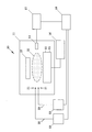
- FIG. 1 is a schematic view of an example of a sputtering apparatus using the thin film forming method of the present invention.
- the sputtering apparatus 10 includes a chamber 11. In the chamber 11, a target 12, an electrode 13, a collimator 14, and a base material 15 are provided.
- the electrode 13 is fixed to the back surface of the target 12 and has the same potential as the target 12.
- the atoms and compounds scattered from the target 12 adhere to the base material 15 and become a thin film (sputtering film).
- a power source 16 a monochromator 17, a PEM control device 18, and a mass flow controller 19 are provided outside the chamber 11.
- the power source 16 is electrically connected to the electrode 13 and adjusts the potential of the electrode 13 and the target 12.
- the monochromator 17 is connected to the collimator 14 by an optical fiber.
- the PEM control device 18 is connected to the monochromator 17 by a signal line.
- the mass flow controller 19 is connected to the PEM control device 18 by a signal line.
- a gas introduction pipe 20 is conducted into the chamber 11, and a gas 21 is supplied into the chamber 11.
- the gas 21 is, for example, a sputtering gas (for example, argon) or a reactive gas (for example, oxygen). Due to the voltage applied between the base material 15 and the target 12, the gas 21 and the constituent materials of the target 12 are converted into plasma in the space between the target 12 and the base material 15, thereby forming a plasma 22.
- the plasma 22 emits plasma light of each of the constituent materials of the gas 21 and the target 12.
- Plasma light is acquired by the collimator 14 and transmitted to the monochromator 17 through an optical fiber.
- the plasma light is decomposed into a spectrum.
- the collimator 14 acquires plasma light in a wide wavelength range, the peak intensity of the plasma light in the narrow wavelength range set by the monochromator 17 is detected.
- the monochromator 17 is a combination of a diffraction grating (not shown), a slit (not shown), and a photomultiplier tube (not shown).
- a wavelength range of light to be detected by the diffraction grating and the slit is set, a specific peak intensity included in the wavelength range is detected by a photomultiplier tube, and converted into an electric signal.
- the center value of the wavelength range can be continuously set to a desired value by adjusting the angle formed by the diffraction grating surface and the diffracted light.
- the wavelength range can be continuously set to a desired value by adjusting the width of the slit through which the diffracted light passes.
- the electrical signal having a specific peak intensity detected by the monochromator 17 is transmitted to the PEM control device 18.
- the PEM control device 18 transmits a signal to the mass flow controller 19 so that the peak intensity of the specific plasma light is constant.
- the mass flow controller 19 adjusts the flow rate of the gas 21 based on the transmitted signal.
- the plasma of each of the deposition material and the gas constituent material is generated, and the surface of the substrate is adjusted while adjusting the gas flow rate (PEM control) with reference to the emission intensity of the plasma. A thin film is formed.
- Step of selecting specific substances First, the intrinsic spectrum of each plasma light of the film forming material and the gas constituent material is investigated, and the constituent material most suitable for PEM control is selected. Such a constituent substance is referred to as a “specific substance”. For example, when the sputtering gas is argon, the reactive gas is oxygen, and the target is silicon, one of argon, oxygen, and silicon is selected as the specific substance.
- the spectrum of plasma light of a specific substance usually includes a plurality of peaks. Among the plurality of peaks of the plasma light of the specific substance, the peak most suitable for PEM control is selected as the “specific peak”. Peaks suitable for PEM control are those that do not have other constituent peaks near the peak. The peaks of other constituent substances in the vicinity become noise when the peak is detected. For example, when oxygen is a specific substance, there are a plurality of oxygen plasma peaks, but an oxygen peak without argon and silicon peaks nearby is selected as the specific peak.
- the step of acquiring the plasma light including the specific peak is executed by making the plasma light incident on the collimator 14, for example. Since the wavelength range of the plasma light acquired by the collimator 14 is wide, the specific peak is usually included therein. In this wavelength range, for example, a plurality of spectra included in the plasma light of the constituent materials (for example, argon, oxygen, silicon) of the gas 21 and the target 12 are superimposed and included. Therefore, PEM control cannot be performed simply by acquiring plasma light and detecting its intensity.
- the constituent materials for example, argon, oxygen, silicon
- the step of decomposing the plasma light into a spectrum is performed, for example, by decomposing light transmitted from the collimator 14 to the monochromator 17 into a spectrum by a diffraction grating (not shown) provided inside the monochromator 17.
- the step of decomposing the plasma light into a spectrum is not limited to the diffraction grating, and may be performed by a prism (not shown), for example.
- the diffraction grating is preferable because it has a higher resolution than the prism and the resolution is less affected by the wavelength.
- Detection wavelength range means a wavelength range in which plasma emission can be detected. Accordingly, the “detection wavelength range of specific peak intensity” means a wavelength range in which the specific peak intensity can be detected. That is, the specific peak wavelength is included in the “detection wavelength range of the specific peak intensity”.
- a wavelength range in which the specific peak is included and the peaks of other constituent substances that cause noise that inhibits the detection of the specific peak intensity is set. When the specific peak and the peak of another constituent are close to each other, the wavelength range must be set narrow.
- the wavelength range can be set by the monochromator 17, but it may not be possible by a bandpass filter (not shown).
- a “wavelength range in which specific peaks are included and peaks of other constituents that cause noise that hinders detection of specific peak intensities” is set. It does not mean that the narrow wavelength range of the pass filter is set. If noise can be eliminated, it is desirable to set a wavelength range as wide as possible. This is because the wider the wavelength range, the higher the S / N ratio (signal / noise ratio) and the higher the detection accuracy.
- the present application is not a simple method of detecting a specific peak intensity in the narrowest wavelength range possible.
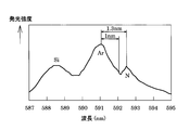
- FIG. 2 shows the spectrum of plasma light near 590 nm.
- the horizontal axis represents wavelength (unit: nm), and the vertical axis represents emission intensity (arbitrary unit).
- An attempt is made to detect an argon (Ar) peak in the spectrum of FIG.
- the argon peak is near 591.2 nm, but there is a nitrogen (N) peak near 592.5 nm. If the center value of the detection wavelength of the monochromator 17 is 591.2 nm and the wavelength range (one side) is 1 nm, the detection range is 590.2 nm to 592.2 nm. At this time, the argon peak falls within the detection range, but the nitrogen peak does not.
- the peak intensity of argon can be detected without receiving the influence (noise) of the peak of nitrogen.
- the wavelength range (one side) is 1.3 nm, for example, the detection range is 589.9 to 592.5 nm, and the nitrogen peak (592.5 nm) also enters the detection range and becomes noise, so the detection accuracy of the argon peak intensity Decreases.
- the detection wavelength range can also be set using a band pass filter (high-precision color filter) (not shown) instead of the monochromator 17.
- a band pass filter high-precision color filter
- the detection (transmission) wavelength range of a commercially available bandpass filter is determined in advance, and the detection wavelength range can only be selected discretely.
- the detection wavelength range of each bandpass filter is considerably wider than that of the monochromator 17, noise may be mixed as will be described later.
- Fig. 3 shows the spectrum of plasma light around 780 nm.
- the horizontal axis represents wavelength (unit: nm), and the vertical axis represents emission intensity (arbitrary unit).
- An attempt is made to detect the peak intensity of oxygen (O) in the spectrum of FIG.
- the oxygen peak is near 776.5 nm, but there is a very strong argon (Ar) peak near 771.5 nm.
- a commercially available bandpass filter cannot select the detection wavelength range freely. If a commercially available bandpass filter is used to detect the peak intensity of oxygen near 776.5 nm, a bandpass filter having a center value of 780 nm and a wavelength range (one side) of 8 nm is generally used. In this case, since the detection range is 772 nm to 788 nm, in addition to the oxygen peak, a part of the argon peak having a higher intensity than the oxygen peak is included. Therefore, the peak intensity of oxygen cannot be detected with high accuracy.
- the center value of the detection wavelength is set to 776.5 nm and the wavelength range (one side) is set to 1 nm using the monochromator 17, the detection range is 775.5 nm to 777.5 nm, so the influence of the argon peak (noise) It is possible to detect the peak intensity of oxygen with high accuracy without being subjected to this.
- the step of detecting the specific peak intensity is used to estimate the amount of plasma of the specific substance. This is performed by, for example, a photomultiplier tube (not shown) provided inside the monochromator 17. Instead of the photomultiplier tube, a CCD (Charge Coupled Device) detector or a CMOS (Complementary Metal Oxide Semiconductor) detector can be used. However, since the operation speed of the CCD detector or the CMOS detector is slower than that of the photomultiplier tube, the photomultiplier tube is preferable when the intensity of the plasma light changes in a short time.
- Step of adjusting gas flow rate with reference to specific peak intensity The step of adjusting the gas flow rate with reference to the specific peak intensity is executed by, for example, the PEM control device 18. By adjusting the gas flow rate with reference to the specific peak intensity, a thin film with little variation in film thickness and film characteristics can be formed.
- Example 1 A silicon oxide (SiO 2 ) thin film was formed by a reactive sputtering method using silicon (Si) as a target, argon (Ar) as a sputtering gas, and oxygen (O 2 ) as a reactive gas.
- White plate glass was used as the substrate 15.
- a DC pulse power source was used as the power source 16. In the region of plasma 22, argon plasma light, oxygen plasma light, and silicon plasma light were observed.
- Plasma light was acquired by the collimator 14 and transmitted to the monochromator 17.
- the monochromator 17 decomposed the plasma light into a spectrum, the center value of the detection wavelength was set to 777 nm close to the oxygen peak, and the wavelength range (one side) was set to 1 nm.
- the peak intensity of the oxygen plasma light detected by the monochromator 17 was converted into an electrical signal and transmitted to the PEM controller 18.
- the PEM control device 18 transmitted a signal to the mass flow controller 19 so that the peak intensity of the oxygen plasma light was constant.
- the mass flow controller 19 adjusted the flow rate of oxygen based on the transmitted signal.
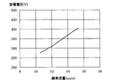
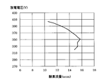
- FIG. 4 shows a graph of oxygen flow rate (unit sccm) and discharge voltage (unit V) when the above control is performed. As shown in the graph of FIG. 4, the discharge voltage appropriately followed the change in the oxygen flow rate, and the PEM control was appropriately performed.
- outgas such as moisture and oxygen is generated from the base material and the like, and the influence thereof may cause variations in the film thickness and characteristics of the thin film in the width direction and flow direction of the base material.
- the plasma state becomes unstable due to the influence of oxygen contained in the outgas, and the film thickness and characteristics of the oxide thin film may vary. Therefore, when forming an oxide thin film, it is required that the plasma state be not affected by oxygen contained in the outgas.
- the sputtering method of the present invention when used, for example, when oxygen is unpredictably generated from the base material 15 as outgas, the peak intensity of the plasma light of oxygen is accurately detected, so that the oxygen generated from the base material 15 can be separated. Only the oxygen supplied through the mass flow controller 19 can be reduced in real time.
- the sum of the amount of oxygen generated from the base material 15 and the amount of oxygen supplied through the mass flow controller 19 can be made constant by PEM control.
- PEM control By performing such PEM control, the plasma 22 is stabilized.
- variations in film thickness and characteristics are less likely to occur in the width direction and flow direction of the substrate 15.
- PEM control is performed to keep the sum of oxygen amounts constant. Delay is unlikely to occur.
- the center value of the detection wavelength was set to 251 nm close to the peak wavelength of silicon, and the wavelength range (one side) was set to 1 nm. Otherwise, the flow rate of oxygen was adjusted in the same manner as described above with reference to the peak intensity of silicon.
- FIG. 5 shows a graph of oxygen flow rate (unit sccm) and discharge voltage (unit V) when the above control is performed. As shown in the graph of FIG. 5, the discharge voltage appropriately followed the change in the oxygen flow rate, and the PEM control was appropriately performed.
- Example 2 A thin film of niobium oxide (Nb 2 O 5 ) was formed by a reactive sputtering method using niobium (Nb) as a target, argon (Ar) as a sputtering gas, and oxygen (O 2 ) as a reactive gas.
- White plate glass was used as the substrate 15.
- a DC pulse power source was used as the power source 16. In the region of the plasma 22, argon plasma light, oxygen plasma light, and niobium plasma light were observed.
- Plasma light was acquired by the collimator 14 and transmitted to the monochromator 17.
- the monochromator 17 decomposed the plasma light into a spectrum, the center value of the detection wavelength was set to 777 nm close to the peak wavelength of oxygen, and the wavelength range (one side) was set to 1 nm.
- the electrical signal of the peak intensity of oxygen detected by the monochromator 17 was transmitted to the PEM controller 18.
- the PEM control device 18 transmitted a signal to the mass flow controller 19 so that the peak intensity of oxygen was constant.
- the mass flow controller 19 adjusted the flow rate of oxygen based on the transmitted signal.
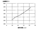
- FIG. 6 shows a graph of the oxygen flow rate (unit sccm) and the discharge voltage (unit V) when the above control is performed. As shown in the graph of FIG. 6, the discharge voltage appropriately followed the change in the oxygen flow rate, and the PEM control was appropriately performed. Although the linearity is broken at the right end of the graph, this portion is not actually used, so there is no practical effect.
- the center value of the detection wavelength was set to 507 nm close to the peak wavelength of niobium, and the wavelength range (one side) was set to 1 nm. Otherwise, the flow rate of oxygen was adjusted in the same manner as above with reference to the peak intensity of niobium.
- FIG. 7 shows a graph of oxygen flow rate (unit sccm) and discharge voltage (unit V) when the above control is performed. As shown in the graph of FIG. 7, the discharge voltage appropriately followed the change in the oxygen flow rate, and the PEM control was appropriately performed. Although the linearity is broken at the right end of the graph, this portion is not actually used, so there is no practical effect.
- a silicon oxide (SiO 2 ) thin film was formed by a reactive sputtering method using silicon (Si) as a target, argon (Ar) as a sputtering gas, and oxygen (O 2 ) as a reactive gas.
- a band pass filter was used instead of the monochromator.
- a bandpass filter with a wavelength range of 772 nm to 788 nm close to the peak wavelength of oxygen was selected.
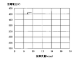
- FIG. 8 shows a graph of the oxygen flow rate (unit sccm) and the discharge voltage (unit V) when the above control is performed. As shown in the graph of FIG. 8, the discharge voltage did not follow the change in the oxygen flow rate, and PEM control was impossible. This is because the bandpass filter has a wide wavelength range, so that light of substances other than silicon, such as argon, enters as noise in addition to the silicon peak, and the peak intensity of silicon cannot be detected accurately.
- niobium oxide Nb 2 O 5
- Ar argon
- oxygen O 2
- a band pass filter was used instead of the monochromator.
- FIG. 9 shows a graph of oxygen flow rate (unit sccm) and discharge voltage (unit V) when the above control is performed.
- the discharge voltage did not follow the change in the oxygen flow rate, and PEM control was impossible. This is because, as shown in FIG. 3, since the bandpass filter has a wide wavelength range, argon light stronger than the oxygen peak enters as noise, and the peak intensity of oxygen cannot be detected accurately.
- niobium oxide Nb 2 O 5
- a bandpass filter having a wavelength of 400 nm to 420 nm close to the peak wavelength of niobium was selected. Otherwise, the flow rate of oxygen gas was adjusted in the same manner as in Example 2 with reference to the peak intensity of niobium. In this case, the PEM control was appropriately performed as in FIG.
- Table 1 shows a summary of examples and comparative examples.
- the wavelength range was set so as to exclude noise that hinders detection of the specific peak intensity.
- PEM control can be performed by referring to any specific peak intensity of oxygen or silicon in Example 1
- PEM control can be performed by referring to any specific peak intensity of oxygen or niobium in Example 2.
- PEM control was possible without being restricted by gas and target material. Therefore, all the evaluations were appropriate ( ⁇ ).
- the center value of the detection wavelength is discretely determined in advance, and a bandpass filter having a wide wavelength range is used. Even when a band-pass filter was used, PEM control was possible when noise that would hinder detection of the specific peak intensity did not enter (when oxygen was referred to in Comparative Example 1 and niobium was referred to in Comparative Example 2).
- the wavelength range could not be set so as to exclude noise that hinders detection of specific peak intensity, so when noise that hinders detection of specific peak intensity entered PEM control was impossible (when silicon was used in Comparative Example 1 and oxygen was used in Comparative Example 2).
- the method for forming a thin film of the present invention is not limited to the sputtering method, and can be applied to other film forming methods such as a plasma CVD method.
- the use of the thin film forming method of the present invention is not limited, but the thin film forming method of the present invention is particularly suitably used when forming a thin film using a reactive sputtering method.
Landscapes
- Chemical & Material Sciences (AREA)
- Engineering & Computer Science (AREA)
- Chemical Kinetics & Catalysis (AREA)
- Organic Chemistry (AREA)
- Metallurgy (AREA)
- Health & Medical Sciences (AREA)
- Mechanical Engineering (AREA)
- Materials Engineering (AREA)
- Physics & Mathematics (AREA)
- Analytical Chemistry (AREA)
- Pathology (AREA)
- Immunology (AREA)
- General Physics & Mathematics (AREA)
- General Health & Medical Sciences (AREA)
- Biochemistry (AREA)
- Life Sciences & Earth Sciences (AREA)
- Nuclear Medicine, Radiotherapy & Molecular Imaging (AREA)
- Plasma & Fusion (AREA)
- Physical Vapour Deposition (AREA)
- Investigating, Analyzing Materials By Fluorescence Or Luminescence (AREA)
- Superconductors And Manufacturing Methods Therefor (AREA)
- Crystals, And After-Treatments Of Crystals (AREA)
Abstract
【課題】プラズマ光を発する物質の種類の制約を受けることなくPEM制御を行なうことができる薄膜の成膜方法。 【解決手段】本発明は、構成物質に含まれる特定物質を選択するステップと、特定物質のプラズマの発する光のスペクトルに含まれる特定ピークを選択するステップと、特定ピークを含むプラズマ光を取得するステップと、プラズマ光をスペクトルに分解するステップと、特定ピーク波長が含まれ特定ピーク強度の検出を阻害するノイズが排除されるように検出波長範囲を設定するステップと、特定ピーク強度を検出するステップと、特定ピーク強度を参照してガスの流量を調整するステップを含む。
Description
本発明は薄膜の成膜方法に関する。
従来から液晶ディスプレイ等に用いられる透明導電膜、各種の光学部品に用いられる反射防止膜や保護膜のような光学薄膜、包装材料に用いられるガスバリア薄膜、磁気記録に用いられる磁気薄膜などの各種薄膜を成膜する方法としてスパッタリング方法が広く用いられている。
スパッタリング方法の一種である反応性スパッタリング方法では、チャンバ内にスパッタリングガスおよび反応性ガスを注入し、スパッタリングガスによってターゲットから叩き出された物質を反応性ガスと反応させながら基材に堆積させる。その際反応性ガスの流量を調整して、膜厚分布や膜特性のばらつきを抑制している。
反応性ガスの流量を調整するための代表的な制御方法として、プラズマエミッションモニタリング制御(以後PEM制御という)が知られている(例えば、特許文献1:特開2002-212720)。PEM制御においては、ターゲットと基材の間に形成されたプラズマの発する光(プラズマの発する光を以後「プラズマ光」という)に含まれる特定の波長の光の強度を一定に保つように反応性ガスの流量を調整する。
スパッタリング方法において観察されるプラズマ光には、スパッタリングガス、反応性ガスおよびターゲットの構成物質のそれぞれのプラズマから発生するプラズマ光が重畳して含まれている。PEM制御において反応性ガスの流量を適切に調整するためには、スパッタリングガス、反応性ガスおよびターゲット物質のそれぞれのプラズマ光のうちのいずれかの強度を精度良く検出する必要がある。
しかし、スパッタリングガス、反応性ガスおよびターゲットの構成物質のそれぞれのプラズマ光の強度のピーク(プラズマ光の強度のピークを以後「ピーク」という)をもたらす波長(プラズマ光の強度のピークをもたらす波長を以後「ピーク波長」という)が互いに近接していると、ピーク波長におけるプラズマ光の強度(ピーク波長におけるプラズマ光の強度を以後「ピーク強度」という)が精度良く検出できない場合がある。この場合、ピーク波長に近接した他の波長のピークがノイズとなり、PEM制御が不能となるおそれがある。
このような事態を避けるため、検出するピークを、近接したピークの無いものに変更することも考えられる。しかしこれを行なうとスパッタリングガス、反応性ガスおよびターゲット材料の選択が制約されるおそれがある。また、目的とする膜によっては検出するピークの変更が不可能なこともある。そのため、検出するピークの変更によりノイズを避ける対策は最善の策とは言えない。
本発明の目的は、プラズマ光を発する物質(例えばスパッタリングガス、反応性ガス、ターゲット材料)の種類の制約を受けることなくPEM制御を行なうことができる薄膜の成膜方法を実現することである。
本願発明者は、薄膜の成膜に用いられるPEM制御において、特定の物質のプラズマ光のピーク強度を検出する際、他の物質のプラズマ光がノイズとして混入しない波長範囲を設定して、特定の物質のプラズマ光のピーク強度を精度良く検出できるようにした。これにより、プラズマ光を発する物質の種類の制約を受けることなくPEM制御ができることを見出し、本発明を完成させた。なお以後、プラズマ光の強度を検出する対象物質を「特定物質」、特定物質のプラズマ光のスペクトルに含まれるピークを「特定ピーク」、特定ピークの波長を「特定ピーク波長」、特定ピークの強度を「特定ピーク強度」という。
(1)本発明は、少なくとも基材、薄膜の成膜材料および薄膜の成膜に使用されるガスが供給されたチャンバ内にて、成膜材料およびガスの構成物質のプラズマを発生させ、プラズマの発光強度を参照してガスの流量を調整しながら基材の表面に薄膜を成膜する薄膜の成膜方法である。
本発明の薄膜の成膜方法は次のステップを含む。
・構成物質に含まれる特定物質を選択するステップ。
・特定物質のプラズマの発する光のスペクトルに含まれる特定ピークを選択するステップ。
・特定ピークを含むプラズマ光を取得するステップ。
・プラズマ光をスペクトルに分解するステップ。
・特定ピーク波長が含まれ、かつ、特定ピーク強度の検出を阻害するノイズが排除されるように、特定ピーク強度の検出波長範囲を設定するステップ。
・検出波長範囲における特定ピーク強度を検出するステップ。
・特定ピーク強度を参照してガスの流量を調整するステップ。
本発明の薄膜の成膜方法は次のステップを含む。
・構成物質に含まれる特定物質を選択するステップ。
・特定物質のプラズマの発する光のスペクトルに含まれる特定ピークを選択するステップ。
・特定ピークを含むプラズマ光を取得するステップ。
・プラズマ光をスペクトルに分解するステップ。
・特定ピーク波長が含まれ、かつ、特定ピーク強度の検出を阻害するノイズが排除されるように、特定ピーク強度の検出波長範囲を設定するステップ。
・検出波長範囲における特定ピーク強度を検出するステップ。
・特定ピーク強度を参照してガスの流量を調整するステップ。
(2)本発明の薄膜の成膜方法においては特定ピーク強度の検出波長範囲を連続的に設定可能である。
(3)本発明の薄膜の成膜方法において特定ピーク強度の検出波長範囲の設定はモノクロメータにより行なわれる。
(4)本発明の薄膜の成膜方法において検出波長範囲は片側1nm以下(上限-下限が2nm以下)である。
本発明により、プラズマ光を発する物質の種類の制約を受けることなくPEM制御を行なうことができる薄膜の成膜方法が実現された。
図1は本発明の薄膜の成膜方法を用いるスパッタリング装置の一例の模式図である。スパッタリング装置10はチャンバ11を備える。チャンバ11の内部には、ターゲット12、電極13、コリメータ14、基材15が備えられている。電極13はターゲット12の背面に固定されており、ターゲット12と同電位である。ターゲット12から飛散した原子や化合物が基材15に付着して薄膜(スパッタリング膜)となる。
チャンバ11の外部には電源16、モノクロメータ17、PEM制御装置18、マスフローコントローラ19が備えられている。
電源16は電極13に導通しており、電極13およびターゲット12の電位を調節する。モノクロメータ17はコリメータ14と光ファイバで結ばれている。PEM制御装置18はモノクロメータ17と信号線で結ばれている。マスフローコントローラ19はPEM制御装置18と信号線で結ばれている。
マスフローコントローラ19からはガス導入管20がチャンバ11内に導通しており、ガス21がチャンバ11内に供給されている。ガス21は、例えばスパッタリングガス(例えばアルゴン)あるいは反応性ガス(例えば酸素)である。基材15とターゲット12の間に印加された電圧により、ターゲット12と基材15の間の空間にはガス21およびターゲット12の構成物質がそれぞれプラズマ化してプラズマ22が形成されている。
プラズマ22は、ガス21およびターゲット12の構成物質のそれぞれのプラズマ光を発する。プラズマ光はコリメータ14で取得され光ファイバを通じてモノクロメータ17に伝送される。モノクロメータ17ではプラズマ光がスペクトルに分解される。コリメータ14では広い波長範囲のプラズマ光が取得されるが、モノクロメータ17により設定された狭い波長範囲のプラズマ光のピーク強度が検出される。
モノクロメータ17は、回折格子(図示しない)とスリット(図示しない)と光電子増倍管(図示しない)を組み合わせたものである。回折格子とスリットで検出する光の波長範囲を設定し、光電子増倍管でその波長範囲に含まれる特定ピーク強度を検出し、電気信号に変換する。モノクロメータ17では、波長範囲の中心値は、回折格子面と回折光のなす角度を調整することにより所望の値に連続的に設定できる。また波長範囲は、回折光の通過するスリットの幅を調整することにより所望の値に連続的に設定できる。
モノクロメータ17で検出された特定ピーク強度の電気信号は、PEM制御装置18に伝送される。PEM制御装置18は、特定プラズマ光のピーク強度が一定となるように、マスフローコントローラ19に信号を伝送する。マスフローコントローラ19は伝送された信号に基づいてガス21の流量を調整する。
[本発明の薄膜の成膜方法]
本発明の薄膜の成膜方法においては、成膜材料およびガスの構成物質のそれぞれのプラズマを発生させ、プラズマの発光強度を参照してガスの流量を調整(PEM制御)しながら基材の表面に薄膜を成膜する。
本発明の薄膜の成膜方法においては、成膜材料およびガスの構成物質のそれぞれのプラズマを発生させ、プラズマの発光強度を参照してガスの流量を調整(PEM制御)しながら基材の表面に薄膜を成膜する。
[特定物質を選択するステップ]
まず成膜材料およびガスの構成物質のそれぞれのプラズマ光の固有スペクトルを調査し、PEM制御に最も適した構成物質を選択する。このような構成物質を「特定物質」という。例えばスパッタリングガスがアルゴン、反応性ガスが酸素、ターゲットがケイ素の場合、アルゴン、酸素、ケイ素のうちの一つを特定物質として選択する。
まず成膜材料およびガスの構成物質のそれぞれのプラズマ光の固有スペクトルを調査し、PEM制御に最も適した構成物質を選択する。このような構成物質を「特定物質」という。例えばスパッタリングガスがアルゴン、反応性ガスが酸素、ターゲットがケイ素の場合、アルゴン、酸素、ケイ素のうちの一つを特定物質として選択する。
[特定ピークを選択するステップ]
特定物質のプラズマ光のスペクトルには通常複数のピークが含まれる。特定物質のプラズマ光の複数のピークの中で、PEM制御に最も適したピークを「特定ピーク」として選択する。PEM制御に適したピークは当該ピークの近くに他の構成物質のピークがないものである。近くにある他の構成物質のピークは当該ピークの検出のときノイズとなる。例えば酸素を特定物質としたとき、酸素のプラズマのピークは複数あるが、近くにアルゴンおよびケイ素のピークのない酸素のピークを特定ピークとして選択する。
特定物質のプラズマ光のスペクトルには通常複数のピークが含まれる。特定物質のプラズマ光の複数のピークの中で、PEM制御に最も適したピークを「特定ピーク」として選択する。PEM制御に適したピークは当該ピークの近くに他の構成物質のピークがないものである。近くにある他の構成物質のピークは当該ピークの検出のときノイズとなる。例えば酸素を特定物質としたとき、酸素のプラズマのピークは複数あるが、近くにアルゴンおよびケイ素のピークのない酸素のピークを特定ピークとして選択する。
[特定ピークを含むプラズマ光を取得するステップ]
特定ピークを含むプラズマ光を取得するステップは、例えばコリメータ14にプラズマ光を入射させることにより実行される。コリメータ14で取得されるプラズマ光の波長範囲は広いため、通常、特定ピークはその中に含まれる。この波長範囲には、例えば、ガス21およびターゲット12の構成物質(例えばアルゴン、酸素、ケイ素)のそれぞれのプラズマ光に含まれる複数のスペクトルが重畳して含まれる。従って単にプラズマ光を取得し、その強度を検出しただけではPEM制御はできない。
特定ピークを含むプラズマ光を取得するステップは、例えばコリメータ14にプラズマ光を入射させることにより実行される。コリメータ14で取得されるプラズマ光の波長範囲は広いため、通常、特定ピークはその中に含まれる。この波長範囲には、例えば、ガス21およびターゲット12の構成物質(例えばアルゴン、酸素、ケイ素)のそれぞれのプラズマ光に含まれる複数のスペクトルが重畳して含まれる。従って単にプラズマ光を取得し、その強度を検出しただけではPEM制御はできない。
[プラズマ光をスペクトルに分解するステップ]
プラズマ光をスペクトルに分解するステップは例えばコリメータ14からモノクロメータ17に伝送された光を、モノクロメータ17の内部に備えられた回折格子(図示しない)によりスペクトルに分解することにより実行される。プラズマ光をスペクトルに分解するステップは回折格子に限らず、例えばプリズム(図示しない)でも可能である。しかし一般に回折格子の方がプリズムより分解能が高く、また分解能が波長の影響を受けにくいため、回折格子の方が好ましい。
プラズマ光をスペクトルに分解するステップは例えばコリメータ14からモノクロメータ17に伝送された光を、モノクロメータ17の内部に備えられた回折格子(図示しない)によりスペクトルに分解することにより実行される。プラズマ光をスペクトルに分解するステップは回折格子に限らず、例えばプリズム(図示しない)でも可能である。しかし一般に回折格子の方がプリズムより分解能が高く、また分解能が波長の影響を受けにくいため、回折格子の方が好ましい。
[特定ピーク強度の検出波長範囲を設定するステップ]
「検出波長範囲」とはプラズマ発光を検出できる波長範囲を意味する。従って「特定ピーク強度の検出波長範囲」とは特定ピーク強度を検出できる波長範囲を意味する。すなわち「特定ピーク強度の検出波長範囲」内に特定ピーク波長が含まれている。特定ピーク強度を検出する波長範囲を設定するステップにおいては、特定ピークが含まれ、かつ、特定ピーク強度の検出を阻害するノイズとなる他の構成物質のピークが排除される波長範囲を設定する。特定ピークと他の構成物質のピークが近接しているときは、波長範囲を狭く設定しなければならない。そのような場合、後述のように、モノクロメータ17では波長範囲の設定が可能であるが、バンドパスフィルタ(図示しない)では不可能なときがある。本願においては「特定ピークが含まれ、かつ、特定ピーク強度の検出を阻害するノイズとなる他の構成物質のピークが排除される波長範囲」を設定するが、これはモノクロメータ17、あるいは、バンドパスフィルタの限界の狭い波長範囲を設定するという意味ではない。ノイズが排除できるならば、できるだけ広い波長範囲を設定する方が望ましい。なぜならば波長範囲が広い方がS/N比(シグナル/ノイズ比)が高くなって検出精度が高くなるからである。本願は、できるだけ狭い波長範囲で特定ピーク強度を検出するという単純な方法ではない。
「検出波長範囲」とはプラズマ発光を検出できる波長範囲を意味する。従って「特定ピーク強度の検出波長範囲」とは特定ピーク強度を検出できる波長範囲を意味する。すなわち「特定ピーク強度の検出波長範囲」内に特定ピーク波長が含まれている。特定ピーク強度を検出する波長範囲を設定するステップにおいては、特定ピークが含まれ、かつ、特定ピーク強度の検出を阻害するノイズとなる他の構成物質のピークが排除される波長範囲を設定する。特定ピークと他の構成物質のピークが近接しているときは、波長範囲を狭く設定しなければならない。そのような場合、後述のように、モノクロメータ17では波長範囲の設定が可能であるが、バンドパスフィルタ(図示しない)では不可能なときがある。本願においては「特定ピークが含まれ、かつ、特定ピーク強度の検出を阻害するノイズとなる他の構成物質のピークが排除される波長範囲」を設定するが、これはモノクロメータ17、あるいは、バンドパスフィルタの限界の狭い波長範囲を設定するという意味ではない。ノイズが排除できるならば、できるだけ広い波長範囲を設定する方が望ましい。なぜならば波長範囲が広い方がS/N比(シグナル/ノイズ比)が高くなって検出精度が高くなるからである。本願は、できるだけ狭い波長範囲で特定ピーク強度を検出するという単純な方法ではない。
一例として、図2に590nm付近のプラズマ光のスペクトルを示す。横軸は波長(単位nm)、縦軸は発光強度(任意単位)である。図2のスペクトルにおいてアルゴン(Ar)のピークを検出することを試みる。アルゴンのピークは591.2nm付近にあるが、すぐ近くの592.5nm付近にチッ素(N)のピークがある。モノクロメータ17の検出波長の中心値を591.2nmとし、波長範囲(片側)を1nmとすると、検出範囲は590.2nm~592.2nmとなる。このときアルゴンのピークは検出範囲に入るが、チッ素のピークは入らない。これによりチッ素のピークの影響(ノイズ)を受けずに、アルゴンのピーク強度が検出できる。この場合、波長範囲(片側)を例えば1.3nmとすると、検出範囲は589.9nm~592.5nmとなり、チッ素のピーク(592.5nm)も検出範囲に入りノイズとなるため、アルゴンのピーク強度の検出精度が低下する。
モノクロメータ17の代わりにバンドパスフィルタ(高精度のカラーフィルタ)(図示しない)を用いて検出波長範囲を設定することもできる。但し市販のバンドパスフィルタの検出(透過)波長範囲は予め定められており、検出波長範囲は離散的にしか選択できない。また個々のバンドパスフィルタの検出波長範囲はモノクロメータ17に比べてかなり広いため、後述するようにノイズが混入するときがある。
一例として図3に780nm付近のプラズマ光のスペクトルを示す。横軸は波長(単位nm)、縦軸は発光強度(任意単位)である。図3のスペクトルにおいて酸素(O)のピーク強度を検出することを試みる。酸素のピークは776.5nm付近にあるが、近くの771.5nm付近に非常に強いアルゴン(Ar)のピークがある。市販のバンドパスフィルタは検出波長範囲を自由に選択することができない。もし市販のバンドパスフィルタにより776.5nm付近にある酸素のピーク強度を検出しようとすると、一般に中心値が780nm、波長範囲(片側)が8nmのバンドパスフィルタが用いられる。その場合、検出範囲は772nm~788nmとなるため、酸素のピークに加えて、酸素のピークより強度の強いアルゴンのピークの一部が入る。そのため酸素のピーク強度を精度良く検出することはできない。
オーダーメイドで所望の検出波長範囲のバンドパスフィルタを作製することも可能である。しかしオーダーメイドのバンドパスフィルタは高額であり、しかもバンドパスフィルタは波長範囲を狭くすると透過率が低下するという問題がある。
それに対してモノクロメータ17を用いて、検出波長の中心値を776.5nm、波長範囲(片側)を1nmに設定すると、検出範囲は775.5nm~777.5nmとなるため、アルゴンのピークの影響(ノイズ)を受けることなく、酸素のピーク強度を精度良く検出することができる。
ガス21あるいはターゲット12の種類によってはバンドパスフィルタを使用しても検出精度の問題がない場合もある。しかしバンドパスフィルタを使用して広い波長範囲の多数の箇所でピーク強度を検出しようとすると、検出波長の異なる多数のバンドパスフィルタを用意する必要がある。このようなことは管理も煩雑であるし経済的にも好ましくない。そのため、バンドパスフィルタよりモノクロメータ17を用いる方が好ましい。
[特定ピーク強度を検出するステップ]
特定ピーク強度の検出を行なうステップは、特定物質のプラズマの量を推定するために用いられる。これは例えばモノクロメータ17の内部に備えられた光電子増倍管(図示しない)により行なわれる。光電子増倍管の代わりに、CCD(Charge Coupled Device)検出器やCMOS(Complementary Metal Oxide Semiconductor)検出器を用いることもできる。しかしCCD検出器やCMOS検出器の動作速度は光電子増倍管に比べて遅いため、プラズマ光の強度が短時間に変化する場合は光電子増倍管の方が好ましい。
特定ピーク強度の検出を行なうステップは、特定物質のプラズマの量を推定するために用いられる。これは例えばモノクロメータ17の内部に備えられた光電子増倍管(図示しない)により行なわれる。光電子増倍管の代わりに、CCD(Charge Coupled Device)検出器やCMOS(Complementary Metal Oxide Semiconductor)検出器を用いることもできる。しかしCCD検出器やCMOS検出器の動作速度は光電子増倍管に比べて遅いため、プラズマ光の強度が短時間に変化する場合は光電子増倍管の方が好ましい。
[特定ピーク強度を参照してガスの流量を調整するステップ]
特定ピーク強度を参照してガスの流量を調整するステップは、例えばPEM制御装置18により実行される。特定ピーク強度を参照してガスの流量を調整することにより、膜厚および膜特性のばらつきの少ない薄膜を成膜することができる。
特定ピーク強度を参照してガスの流量を調整するステップは、例えばPEM制御装置18により実行される。特定ピーク強度を参照してガスの流量を調整することにより、膜厚および膜特性のばらつきの少ない薄膜を成膜することができる。
[実施例および比較例]
[実施例1]
ターゲットとしてケイ素(Si)を、スパッタリングガスとしてアルゴン(Ar)を、反応性ガスとして酸素(O2)を用いて、反応性スパッタリング方法により酸化ケイ素(SiO2)の薄膜を成膜した。基材15として白板ガラスを用いた。電源16としてDCパルス電源を用いた。プラズマ22の領域にはアルゴンのプラズマ光、酸素のプラズマ光、ケイ素のプラズマ光が観察された。
[実施例1]
ターゲットとしてケイ素(Si)を、スパッタリングガスとしてアルゴン(Ar)を、反応性ガスとして酸素(O2)を用いて、反応性スパッタリング方法により酸化ケイ素(SiO2)の薄膜を成膜した。基材15として白板ガラスを用いた。電源16としてDCパルス電源を用いた。プラズマ22の領域にはアルゴンのプラズマ光、酸素のプラズマ光、ケイ素のプラズマ光が観察された。
プラズマ光をコリメータ14で取得し、モノクロメータ17に伝送した。モノクロメータ17でプラズマ光をスペクトルに分解し、検出波長の中心値を酸素のピークに近い777nmに設定し、波長範囲(片側)を1nmに設定した。
モノクロメータ17で検出された酸素のプラズマ光のピーク強度は電気信号に変換されてPEM制御装置18に伝送された。PEM制御装置18は、酸素のプラズマ光のピーク強度が一定となるように、マスフローコントローラ19に信号を伝送した。マスフローコントローラ19は伝送された信号に基づいて酸素の流量を調整した。
図4に、上記の制御を行なったときの、酸素流量(単位sccm)と放電電圧(単位V)のグラフを示す。図4のグラフに示すように、放電電圧は酸素流量の変化に適切に追随しており、PEM制御が適切に行なわれていた。
スパッタリングの際、基材等から水分、酸素等のアウトガスが発生し、その影響により、基材の幅方向や流れ方向において薄膜の膜厚や特性のばらつきが生じることがある。
例えば酸化物薄膜を成膜する場合、アウトガスに含まれる酸素の影響によりプラズマの状態が不安定となり、酸化物薄膜の膜厚や特性がばらつくことがある。そのため、酸化物薄膜を形成する場合、プラズマの状態が、アウトガスに含まれる酸素の影響を受けないようにすることが求められている。
本発明のスパッタリング方法を用いれば、例えば基材15からアウトガスとして酸素が予測不可能に発生する場合、酸素のプラズマ光のピーク強度を精度良く検出することにより、基材15から発生した酸素の分だけ、マスフローコントローラ19を通して供給する酸素をリアルタイムに減らすことができる。
これにより、基材15から発生した酸素の量とマスフローコントローラ19を通して供給する酸素の量の和をPEM制御により一定にすることができる。このようなPEM制御を行なうことによりプラズマ22が安定する。プラズマ22が安定すると、基材15の幅方向や流れ方向において膜厚や特性のばらつきが生じにくい。前述のようにモノクロメータ17内の光電子増倍管の動作速度が極めて速いため、基材15から発生する酸素の量が急激に変化するときでも、酸素の量の和を一定にするPEM制御に遅れが生じにくい。
同じく酸化ケイ素(SiO2)の薄膜を成膜する際、検出波長の中心値を、ケイ素のピーク波長に近い251nmに設定し、波長範囲(片側)を1nmに設定した。それ以外は上記と同様にしてケイ素のピーク強度を参照して酸素の流量を調整した。
図5に、上記の制御を行なったときの、酸素流量(単位sccm)と放電電圧(単位V)のグラフを示す。図5のグラフに示すように、放電電圧は酸素流量の変化に適切に追随しており、PEM制御が適切に行なわれていた。
[実施例2]
ターゲットとしてニオブ(Nb)を、スパッタリングガスとしてアルゴン(Ar)を、反応性ガスとして酸素(O2)を用いて、反応性スパッタリング方法により酸化ニオブ(Nb2O5)の薄膜を成膜した。基材15として白板ガラスを用いた。電源16としてDCパルス電源を用いた。プラズマ22の領域には、アルゴンのプラズマ光、酸素のプラズマ光、ニオブのプラズマ光が観察された。
ターゲットとしてニオブ(Nb)を、スパッタリングガスとしてアルゴン(Ar)を、反応性ガスとして酸素(O2)を用いて、反応性スパッタリング方法により酸化ニオブ(Nb2O5)の薄膜を成膜した。基材15として白板ガラスを用いた。電源16としてDCパルス電源を用いた。プラズマ22の領域には、アルゴンのプラズマ光、酸素のプラズマ光、ニオブのプラズマ光が観察された。
プラズマ光をコリメータ14で取得し、モノクロメータ17に伝送した。モノクロメータ17でプラズマ光をスペクトルに分解し、検出波長の中心値を、酸素のピーク波長に近い777nmに設定し、波長範囲(片側)を1nmに設定した。
モノクロメータ17で検出された酸素のピーク強度の電気信号は、PEM制御装置18に伝送された。PEM制御装置18は、酸素のピーク強度が一定となるように、マスフローコントローラ19に信号を伝送した。マスフローコントローラ19は伝送された信号に基づいて酸素の流量を調整した。
図6に、上記の制御を行なったときの、酸素流量(単位sccm)と放電電圧(単位V)のグラフを示す。図6のグラフに示すように、放電電圧は酸素流量の変化に適切に追随しており、PEM制御が適切に行なわれていた。なおグラフの右端ではリニアリティが崩れているが、この部分は実際には使用されないため、実用上の影響はない。
同じく酸化ニオブ(Nb2O5)の薄膜を成膜する際、検出波長の中心値をニオブのピーク波長に近い507nmに設定し、波長範囲(片側)を1nmに設定した。それ以外は上記と同様にしてニオブのピーク強度を参照して酸素の流量を調整した。
図7に、上記の制御を行なったときの、酸素流量(単位sccm)と放電電圧(単位V)のグラフを示す。図7のグラフに示すように、放電電圧は酸素流量の変化に適切に追随しており、PEM制御が適切に行なわれていた。なおグラフの右端ではリニアリティが崩れているが、この部分は実際には使用されないため、実用上の影響はない。
[比較例1]
ターゲットとしてケイ素(Si)を、スパッタリングガスとしてアルゴン(Ar)を、反応性ガスとして酸素(O2)を用いて、反応性スパッタリング方法により酸化ケイ素(SiO2)の薄膜を成膜した。モノクロメータの代わりにバンドパスフィルタを用いた。バンドパスフィルタは波長範囲が酸素のピーク波長に近い772nm~788nmのものを選択した。それ以外は実施例1と同様にして酸素のピーク強度を参照して酸素の流量を調整した。この場合図4と同様にPEM制御は適切に行なわれていた。
ターゲットとしてケイ素(Si)を、スパッタリングガスとしてアルゴン(Ar)を、反応性ガスとして酸素(O2)を用いて、反応性スパッタリング方法により酸化ケイ素(SiO2)の薄膜を成膜した。モノクロメータの代わりにバンドパスフィルタを用いた。バンドパスフィルタは波長範囲が酸素のピーク波長に近い772nm~788nmのものを選択した。それ以外は実施例1と同様にして酸素のピーク強度を参照して酸素の流量を調整した。この場合図4と同様にPEM制御は適切に行なわれていた。
同じく酸化ケイ素(SiO2)の薄膜を成膜する際、バンドパスフィルタとして波長範囲がケイ素のピークに近い280nm~296nmのものを選択した。それ以外は上記と同様にしてケイ素のピーク強度を参照して酸素ガスの流量を調整した。図8に、上記の制御を行なったときの、酸素流量(単位sccm)と放電電圧(単位V)のグラフを示す。図8のグラフに示すように、放電電圧は酸素流量の変化に追随しておらず、PEM制御不能であった。この理由は、バンドパスフィルタの波長範囲が広いため、ケイ素のピーク以外にもアルゴンなどのケイ素以外の物質の光がノイズとして入り込み、ケイ素のピーク強度が精度良く検出できなかったためである。
[比較例2]
ターゲットとしてニオブ(Nb)を、スパッタリングガスとしてアルゴン(Ar)を、反応性ガスとして酸素(O2)を用いて、反応性スパッタリング方法により酸化ニオブ(Nb2O5)の薄膜を成膜した。モノクロメータの代わりにバンドパスフィルタを用いた。バンドパスフィルタは波長範囲が酸素のピーク波長に近い772nm~788nmのものを選択した。それ以外は実施例2と同様にして酸素のピーク強度を参照して酸素ガスの流量を調整した。
ターゲットとしてニオブ(Nb)を、スパッタリングガスとしてアルゴン(Ar)を、反応性ガスとして酸素(O2)を用いて、反応性スパッタリング方法により酸化ニオブ(Nb2O5)の薄膜を成膜した。モノクロメータの代わりにバンドパスフィルタを用いた。バンドパスフィルタは波長範囲が酸素のピーク波長に近い772nm~788nmのものを選択した。それ以外は実施例2と同様にして酸素のピーク強度を参照して酸素ガスの流量を調整した。
図9に、上記の制御を行なったときの、酸素流量(単位sccm)と放電電圧(単位V)のグラフを示す。図9のグラフに示すように、放電電圧は酸素流量の変化に追随しておらず、PEM制御不能であった。この理由は、図3に示したように、バンドパスフィルタの波長範囲が広いため、酸素のピークより強いアルゴンの光がノイズとして入り込み、酸素のピーク強度が精度良く検出できなかったためである。
同じく酸化ニオブ(Nb2O5)の薄膜を成膜する際、バンドパスフィルタとしてニオブのピーク波長に近い400nm~420nmのものを選択した。それ以外は実施例2と同様にしてニオブのピーク強度を参照して酸素ガスの流量を調整した。この場合は図7と同様にPEM制御は適切に行なわれていた。
表1に実施例、比較例のまとめを示す。

実施例1、2においては、特定ピーク強度の検出を阻害するノイズを除くように波長範囲が設定された。これにより、実施例1においては酸素とケイ素のいずれの特定ピーク強度を参照してもPEM制御が可能であり、実施例2においては酸素とニオブのいずれの特定ピーク強度を参照してもPEM制御が可能であった。すなわちガスおよびターゲット材料の制約を受けることなくPEM制御を行なうことができた。従って評価はいずれも適切(○)であった。
比較例1、2においては、検出波長の中心値が予め離散的に定められており、しかも波長範囲が広いバンドパスフィルタを用いている。バンドパスフィルタを用いた場合でも、特定ピーク強度の検出を阻害するようなノイズが入らないときはPEM制御が可能であった(比較例1で酸素、比較例2でニオブを参照した場合)。
しかし複数のピークが近接している場合、特定ピーク強度の検出を阻害するノイズを除くように波長範囲を設定することができなかったため、特定ピーク強度の検出を阻害するようなノイズが入ったときはPEM制御が不可能であった(比較例1でケイ素、比較例2で酸素を用いた場合)。
上記のように比較例1、2においてはPEM制御に用いるガスあるいはターゲットの物質が制約されてしまうため不都合が生じるおそれがある。従って評価はいずれも不適切(X)であった。
[モノクロメータ]
モノクロメータとして堀場ジョバンイボン社製プラズマモニタH-20Vを使用した。
モノクロメータとして堀場ジョバンイボン社製プラズマモニタH-20Vを使用した。
[PEM制御装置]
PEM制御装置としてGencoa社製Speedfloを使用した。
PEM制御装置としてGencoa社製Speedfloを使用した。
なお本発明の薄膜の成膜方法は、スパッタリング方法に限定されず、他の成膜方法、例えば、プラズマCVD方法などにも応用可能である。
本発明の薄膜の成膜方法の用途に制限は無いが、本発明の薄膜の成膜方法は反応性スパッタリング方法を用いて薄膜を成膜する際に特に好適に用いられる。
Claims (4)
- 少なくとも基材、薄膜の成膜材料および前記薄膜の成膜に使用されるガスが供給されたチャンバ内にて、前記成膜材料および前記ガスの構成物質のそれぞれのプラズマを発生させ、前記プラズマの発光強度を参照して前記ガスの流量を調整しながら前記基材の表面に前記薄膜を成膜する薄膜の成膜方法であって、
前記構成物質に含まれる特定物質を選択するステップと、
前記特定物質のプラズマの発する光のスペクトルに含まれる特定ピークを選択するステップと、
前記特定ピークを含むプラズマ光を取得するステップと、
前記プラズマ光をスペクトルに分解するステップと、
前記特定ピークの波長すなわち特定ピーク波長が含まれ、かつ、前記特定ピークの強度すなわち特定ピーク強度の検出を阻害するノイズが排除されるように、前記特定ピーク強度の検出波長範囲を設定するステップと、
前記検出波長範囲における前記特定ピーク強度を検出するステップと、
前記特定ピーク強度を参照して前記ガスの流量を調整するステップを含むことを特徴とする薄膜の成膜方法。 - 前記特定ピーク強度の検出波長範囲を連続的に設定可能なことを特徴とする請求項1に記載の薄膜の成膜方法。
- 前記特定ピーク強度の検出波長範囲の設定がモノクロメータにより行なわれることを特徴とする請求項1または2に記載の薄膜の成膜方法。
- 前記検出波長範囲が片側1nm以下であることを特徴とする請求項1~3のいずれかに記載の薄膜の成膜方法。
Priority Applications (1)
| Application Number | Priority Date | Filing Date | Title |
|---|---|---|---|
| KR1020167029277A KR102443296B1 (ko) | 2015-02-17 | 2016-01-25 | 박막의 성막 방법 |
Applications Claiming Priority (2)
| Application Number | Priority Date | Filing Date | Title |
|---|---|---|---|
| JP2015028836A JP6670546B2 (ja) | 2015-02-17 | 2015-02-17 | 薄膜の成膜方法 |
| JP2015-028836 | 2015-02-17 |
Publications (1)
| Publication Number | Publication Date |
|---|---|
| WO2016132823A1 true WO2016132823A1 (ja) | 2016-08-25 |
Family
ID=56688797
Family Applications (1)
| Application Number | Title | Priority Date | Filing Date |
|---|---|---|---|
| PCT/JP2016/052046 Ceased WO2016132823A1 (ja) | 2015-02-17 | 2016-01-25 | 薄膜の成膜方法 |
Country Status (3)
| Country | Link |
|---|---|
| JP (1) | JP6670546B2 (ja) |
| KR (1) | KR102443296B1 (ja) |
| WO (1) | WO2016132823A1 (ja) |
Families Citing this family (2)
| Publication number | Priority date | Publication date | Assignee | Title |
|---|---|---|---|---|
| KR102161472B1 (ko) * | 2019-12-09 | 2020-10-06 | 주식회사 아바코 | 스퍼터링장치 및 스퍼터링장치 제어방법 |
| US12205805B2 (en) * | 2021-07-20 | 2025-01-21 | Canon Kabushiki Kaisha | Sputtering apparatus, film formation method, and method for manufacturing product |
Citations (2)
| Publication number | Priority date | Publication date | Assignee | Title |
|---|---|---|---|---|
| JPH10152773A (ja) * | 1996-11-22 | 1998-06-09 | Sony Corp | スパツタ装置及びスパツタ方法 |
| JP2008251866A (ja) * | 2007-03-30 | 2008-10-16 | Hitachi High-Technologies Corp | プラズマ処理装置 |
Family Cites Families (3)
| Publication number | Priority date | Publication date | Assignee | Title |
|---|---|---|---|---|
| JP2002212720A (ja) | 2001-01-23 | 2002-07-31 | Canon Inc | スパッタリング方法およびスパッタリング装置 |
| JP2003268540A (ja) * | 2002-03-08 | 2003-09-25 | Mitsubishi Electric Corp | 成膜方法および成膜装置 |
| JP6101533B2 (ja) * | 2013-03-27 | 2017-03-22 | 株式会社Screenホールディングス | 酸化アルミニウムの成膜方法 |
-
2015
- 2015-02-17 JP JP2015028836A patent/JP6670546B2/ja active Active
-
2016
- 2016-01-25 KR KR1020167029277A patent/KR102443296B1/ko active Active
- 2016-01-25 WO PCT/JP2016/052046 patent/WO2016132823A1/ja not_active Ceased
Patent Citations (2)
| Publication number | Priority date | Publication date | Assignee | Title |
|---|---|---|---|---|
| JPH10152773A (ja) * | 1996-11-22 | 1998-06-09 | Sony Corp | スパツタ装置及びスパツタ方法 |
| JP2008251866A (ja) * | 2007-03-30 | 2008-10-16 | Hitachi High-Technologies Corp | プラズマ処理装置 |
Also Published As
| Publication number | Publication date |
|---|---|
| JP6670546B2 (ja) | 2020-03-25 |
| JP2016151040A (ja) | 2016-08-22 |
| KR20170117308A (ko) | 2017-10-23 |
| KR102443296B1 (ko) | 2022-09-14 |
Similar Documents
| Publication | Publication Date | Title |
|---|---|---|
| US10976242B2 (en) | System and method for monitoring atomic absorption during a surface modification process | |
| EP2735018B1 (de) | Verfahren und vorrichtung zur herstellung partikelarmer schichten auf substraten | |
| AT17188U1 (de) | Optischer filter und sensorsystem | |
| EP2985579B1 (de) | Spektrometer mit monochromator und order-sorting-filter | |
| JP6670546B2 (ja) | 薄膜の成膜方法 | |
| US20180265961A1 (en) | Reactive sputtering apparatus and reactive sputtering method | |
| EP1592821B1 (de) | Verfahren zur herstellung einer multilayerschicht und vorrichtung zur durchführung des verfahrens | |
| CN104350380B (zh) | 测量装置和成膜装置 | |
| JPWO2014033784A1 (ja) | 光学フィルターの製造方法 | |
| JPWO2015004755A1 (ja) | 光学式膜厚計,薄膜形成装置及び膜厚測定方法 | |
| DE10341513B4 (de) | Verfahren zur Regelung des Reaktivgasflusses in reaktiven plasmagestützten Vakuumbeschichtungsprozessen | |
| JP5246862B2 (ja) | スパッタリング装置 | |
| Wallendorf et al. | Optical investigations in a PEM controlled reactive magnetron sputter process for aluminium doped zinc oxide layers using metallic alloy targets | |
| Thöny et al. | Innovative sputter system for high volume production of demanding optical interference coatings | |
| DE102009059097B4 (de) | Verfahren und Vorrichtung zur Auswertung des von einem Plasma emittierten Lichtes zur Regelung von plasmagestützten Vakuumprozessen | |
| JP2012158808A (ja) | 成膜装置および成膜方法 | |
| JP6892743B2 (ja) | 製膜装置 | |
| JP2003247065A (ja) | 薄膜形成装置 | |
| Chesaux et al. | Rotating target source: novel shaperless concept for magnetron sputtering with excellent uniformity | |
| JP2006330485A (ja) | 薄膜形成装置及び薄膜形成方法並びに光学薄膜 | |
| JPS62180070A (ja) | スパツタリング装置 | |
| JP2004061810A (ja) | 多層膜光学フィルター形成装置、および多層膜光学フィルターの製造方法 | |
| Cruz Gabarain et al. | Optimization of deposition parameters for silicon dioxide thin films synthesized by reactive pulsed-direct current magnetron sputtering | |
| WO2024175257A1 (de) | Prozessanordnung | |
| DE3803840A1 (de) | Fotometer |
Legal Events
| Date | Code | Title | Description |
|---|---|---|---|
| 121 | Ep: the epo has been informed by wipo that ep was designated in this application |
Ref document number: 16752212 Country of ref document: EP Kind code of ref document: A1 |
|
| ENP | Entry into the national phase |
Ref document number: 20167029277 Country of ref document: KR Kind code of ref document: A |
|
| NENP | Non-entry into the national phase |
Ref country code: DE |
|
| 122 | Ep: pct application non-entry in european phase |
Ref document number: 16752212 Country of ref document: EP Kind code of ref document: A1 |