WO2016132767A1 - 圧電振動デバイス及びその製造方法 - Google Patents
圧電振動デバイス及びその製造方法 Download PDFInfo
- Publication number
- WO2016132767A1 WO2016132767A1 PCT/JP2016/050563 JP2016050563W WO2016132767A1 WO 2016132767 A1 WO2016132767 A1 WO 2016132767A1 JP 2016050563 W JP2016050563 W JP 2016050563W WO 2016132767 A1 WO2016132767 A1 WO 2016132767A1
- Authority
- WO
- WIPO (PCT)
- Prior art keywords
- base member
- frame
- covering material
- vibration device
- shaped sealing
- Prior art date
- Legal status (The legal status is an assumption and is not a legal conclusion. Google has not performed a legal analysis and makes no representation as to the accuracy of the status listed.)
- Ceased
Links
Images




Classifications
-
- H—ELECTRICITY
- H03—ELECTRONIC CIRCUITRY
- H03H—IMPEDANCE NETWORKS, e.g. RESONANT CIRCUITS; RESONATORS
- H03H9/00—Networks comprising electromechanical or electro-acoustic elements; Electromechanical resonators
- H03H9/02—Details
- H03H9/05—Holders or supports
- H03H9/10—Mounting in enclosures
-
- H—ELECTRICITY
- H03—ELECTRONIC CIRCUITRY
- H03H—IMPEDANCE NETWORKS, e.g. RESONANT CIRCUITS; RESONATORS
- H03H3/00—Apparatus or processes specially adapted for the manufacture of impedance networks, resonating circuits, resonators
- H03H3/007—Apparatus or processes specially adapted for the manufacture of impedance networks, resonating circuits, resonators for the manufacture of electromechanical resonators or networks
- H03H3/02—Apparatus or processes specially adapted for the manufacture of impedance networks, resonating circuits, resonators for the manufacture of electromechanical resonators or networks for the manufacture of piezoelectric or electrostrictive resonators or networks
-
- H—ELECTRICITY
- H03—ELECTRONIC CIRCUITRY
- H03H—IMPEDANCE NETWORKS, e.g. RESONANT CIRCUITS; RESONATORS
- H03H9/00—Networks comprising electromechanical or electro-acoustic elements; Electromechanical resonators
- H03H9/02—Details
- H03H9/05—Holders or supports
- H03H9/10—Mounting in enclosures
- H03H9/1007—Mounting in enclosures for bulk acoustic wave [BAW] devices
- H03H9/1014—Mounting in enclosures for bulk acoustic wave [BAW] devices the enclosure being defined by a frame built on a substrate and a cap, the frame having no mechanical contact with the BAW device
- H03H9/1021—Mounting in enclosures for bulk acoustic wave [BAW] devices the enclosure being defined by a frame built on a substrate and a cap, the frame having no mechanical contact with the BAW device the BAW device being of the cantilever type
-
- H—ELECTRICITY
- H03—ELECTRONIC CIRCUITRY
- H03H—IMPEDANCE NETWORKS, e.g. RESONANT CIRCUITS; RESONATORS
- H03H9/00—Networks comprising electromechanical or electro-acoustic elements; Electromechanical resonators
- H03H9/02—Details
- H03H9/125—Driving means, e.g. electrodes, coils
- H03H9/13—Driving means, e.g. electrodes, coils for networks consisting of piezoelectric or electrostrictive materials
-
- H—ELECTRICITY
- H03—ELECTRONIC CIRCUITRY
- H03H—IMPEDANCE NETWORKS, e.g. RESONANT CIRCUITS; RESONATORS
- H03H9/00—Networks comprising electromechanical or electro-acoustic elements; Electromechanical resonators
- H03H9/15—Constructional features of resonators consisting of piezoelectric or electrostrictive material
- H03H9/17—Constructional features of resonators consisting of piezoelectric or electrostrictive material having a single resonator
- H03H9/19—Constructional features of resonators consisting of piezoelectric or electrostrictive material having a single resonator consisting of quartz
-
- H—ELECTRICITY
- H10—SEMICONDUCTOR DEVICES; ELECTRIC SOLID-STATE DEVICES NOT OTHERWISE PROVIDED FOR
- H10N—ELECTRIC SOLID-STATE DEVICES NOT OTHERWISE PROVIDED FOR
- H10N30/00—Piezoelectric or electrostrictive devices
- H10N30/01—Manufacture or treatment
- H10N30/02—Forming enclosures or casings
-
- H—ELECTRICITY
- H10—SEMICONDUCTOR DEVICES; ELECTRIC SOLID-STATE DEVICES NOT OTHERWISE PROVIDED FOR
- H10N—ELECTRIC SOLID-STATE DEVICES NOT OTHERWISE PROVIDED FOR
- H10N30/00—Piezoelectric or electrostrictive devices
- H10N30/01—Manufacture or treatment
- H10N30/06—Forming electrodes or interconnections, e.g. leads or terminals
-
- H—ELECTRICITY
- H10—SEMICONDUCTOR DEVICES; ELECTRIC SOLID-STATE DEVICES NOT OTHERWISE PROVIDED FOR
- H10N—ELECTRIC SOLID-STATE DEVICES NOT OTHERWISE PROVIDED FOR
- H10N30/00—Piezoelectric or electrostrictive devices
- H10N30/01—Manufacture or treatment
- H10N30/07—Forming of piezoelectric or electrostrictive parts or bodies on an electrical element or another base
-
- H—ELECTRICITY
- H03—ELECTRONIC CIRCUITRY
- H03H—IMPEDANCE NETWORKS, e.g. RESONANT CIRCUITS; RESONATORS
- H03H3/00—Apparatus or processes specially adapted for the manufacture of impedance networks, resonating circuits, resonators
- H03H3/007—Apparatus or processes specially adapted for the manufacture of impedance networks, resonating circuits, resonators for the manufacture of electromechanical resonators or networks
- H03H3/02—Apparatus or processes specially adapted for the manufacture of impedance networks, resonating circuits, resonators for the manufacture of electromechanical resonators or networks for the manufacture of piezoelectric or electrostrictive resonators or networks
- H03H2003/022—Apparatus or processes specially adapted for the manufacture of impedance networks, resonating circuits, resonators for the manufacture of electromechanical resonators or networks for the manufacture of piezoelectric or electrostrictive resonators or networks the resonators or networks being of the cantilever type
Definitions
- the present invention relates to a piezoelectric vibration device and a manufacturing method thereof.
- a quartz piece is mounted on a rectangular ceramic substrate, and the front and back of the substrate are electrically connected by through terminals formed on the side wall of the ceramic substrate
- an extraction terminal connected to the electrode of the crystal piece can be formed on the surface of the substrate, and the extraction terminal can be electrically connected to the mounting terminal formed on the back surface of the substrate (see Patent Document 1). .
- electrodes such as lead terminals and through terminals formed on the ceramic substrate pass through the edge from the surface of the ceramic substrate to the side surface.
- the electrode formed on the edge of the ceramic substrate is subject to wear.
- the electrode since the electrode is exposed to the outside at the edge, the electrode may be damaged. could occur.
- the present invention has been made in view of such circumstances, and an object thereof is to improve electrical connection reliability by preventing disconnection of electrodes.
- a piezoelectric vibration device includes a piezoelectric vibrator having an excitation electrode formed thereon, a base member having a substantially rectangular outer shape, and the piezoelectric vibrator provided on a first surface;
- An external electrode formed continuously from the first surface through the side surface of the base member to the second surface opposite to the first surface of the base member, and opened to face the first surface of the base member
- a lid member having a recess and joined to the base member so as to hermetically seal the piezoelectric vibrator in the internal space between the recess and the base member, and the first surface of the base member among the external electrodes;
- An edge portion constituted by the side surfaces is at least partially covered with a covering material having insulating properties.
- the edge portion constituted by the first surface and the side surface of the base member of the external electrode is at least partially covered with the covering material, so that the electrode exposure is suppressed at the edge portion. Therefore, it is possible to prevent disconnection of the electrode. Therefore, the electrical connection reliability can be improved.
- the covering material is formed integrally with the frame-shaped sealing portion provided along the opening edge of the concave portion of the lid member on the first surface of the base member, And an extending portion that extends from the frame-shaped sealing portion so as to at least partially cover the edge of the external electrode.
- the lid member is joined to the base member via a sealing material provided along the opening edge of the recess, and the covering material surrounds the sealing material on the first surface of the base member.
- the covering material may be formed of a resin material.
- the covering material may be formed of a glass material.
- the adhesion strength between the covering material and the base member can be improved.
- the base member has a cut-out side surface formed by cutting a part of the side surface, and the external electrode passes from the first surface of the base member through the cut-out side surface, You may form continuously over the 2nd surface of a member.
- the cut-out side surface may be formed by cutting a corner portion adjacent to the two side surfaces.
- the extending portion may extend to the second surface along the side surface of the base member.
- the extending portion may extend to a position between the first surface and the second surface along the side surface of the base member.
- the step due to the extending portion serves as a stopper, for example, it is possible to prevent the solder from creeping up during the reflow process. Further, when the coating material is formed of a resin material or a glass material, the solder does not get wet with the coating material, and it is possible to prevent the solder from creeping up.
- a plurality of external electrodes may be provided, and the extending portion may be formed corresponding to each of the plurality of external electrodes.
- the entire edge of the external electrode may be covered with a covering material.
- the covering material is integrally formed with the frame-shaped sealing portion made of a glass material provided along the opening edge of the concave portion of the lid member on the first surface of the base member, and the frame-shaped sealing portion.
- the adhesion strength between the covering material and the base member can be improved.
- a method of manufacturing a piezoelectric vibration device includes: (a) forming a piezoelectric vibrator on which excitation electrodes are formed; and (b) a base member having a substantially rectangular outer shape, Forming a base member having external electrodes continuously formed from the first surface of the base member through the side surface of the base member to the second surface opposite to the first surface of the base member; (c) the external electrode; Among them, an edge portion constituted by the first surface and the side surface of the base member is at least partially covered with an insulating covering material, and (d) the piezoelectric vibrator is mounted on the first surface of the base member.
- a lid member having a recess opened so as to face the first surface of the base member, and a base so that the piezoelectric vibrator is hermetically sealed in an internal space between the recess and the base member.
- the edge portion constituted by the first surface and the side surface of the base member among the external electrodes is at least partially covered with the covering material, the electrode exposure is suppressed at the edge portion, and the electrode Can be prevented. Therefore, the electrical connection reliability can be improved.
- the covering material includes a frame-shaped sealing portion made of a glass material provided along the opening edge of the concave portion of the lid member on the first surface of the base member, and the frame-shaped sealing portion An extension part made of a glass material integrally formed with the extension part extended from the frame-shaped sealing part so as to at least partially cover the edge part of the external electrode,
- the covering member is temporarily fired.
- the covering member is May be fired.
- the lid member is joined to the base member via the sealing material provided along the opening edge of the concave portion, and the covering material is the first member of the base member.
- a frame-shaped guide portion that is formed on one surface so as to surround the sealing material, and is formed integrally with the frame-shaped guide portion and extends from the frame-shaped guide portion so as to at least partially cover the edge of the external electrode. An extended portion.
- the covering material includes a frame-shaped sealing portion made of a glass material provided along the opening edge of the concave portion of the lid member on the first surface of the base member, and the frame-shaped sealing portion An extension part made of a glass material integrally formed with the extension part extended from the frame-shaped sealing part so as to at least partially cover the edge part of the external electrode,
- the covering material is fired.
- the covering material is thermally cured. May be.
- the electrical connection reliability can be improved by preventing the disconnection of the electrodes.
- FIG. 1 is an exploded perspective view of the piezoelectric vibrating device according to the first embodiment of the present invention.
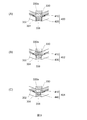
- 2 is a cross-sectional view taken along line II-II in FIG. 3A to 3C are partially enlarged views of the piezoelectric vibration device according to the first embodiment of the present invention.
- FIG. 4 is a diagram showing a modification of the first embodiment of the present invention.
- FIG. 5 is a diagram illustrating the method for manufacturing the piezoelectric vibrating device according to the first embodiment of the invention.
- FIG. 6 is an exploded perspective view of the piezoelectric vibration device according to the second embodiment of the present invention.
- 7 is a cross-sectional view taken along line VII-VII in FIG. FIG.
- FIG. 8 is an exploded perspective view of the piezoelectric vibration device according to the third embodiment of the present invention.
- 9 is a cross-sectional view taken along line IX-IX in FIG.
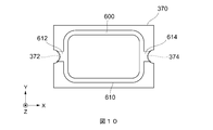
- FIG. 10 is a plan view of a piezoelectric vibration device according to a fourth embodiment of the present invention.
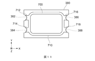
- FIG. 11 is a diagram showing a modification of the fourth embodiment of the present invention.
- FIG. 1 is an exploded perspective view of the piezoelectric vibration device according to the present embodiment
- FIG. 2 is a cross-sectional view taken along the line II-II of FIG. 3A to 3C are partial enlarged views of the base member, and are diagrams for explaining a specific configuration of the covering material according to the present embodiment.
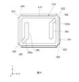
- FIG. 4 is a figure for demonstrating the modification of a base member.
- the piezoelectric vibration device 1 includes a piezoelectric vibrator 100, a lid member 200, and a base member 300.
- the lid member 200 and the base member 300 are cases or packages for accommodating the piezoelectric vibrator 100.
- the piezoelectric vibrator 100, the lid member 200, and the base member 300 have substantially the same size and shape in an XY plan view, for example, a substantially rectangular shape having a longitudinal direction parallel to the X direction and a short direction parallel to the Y direction. It has the outer shape.
- the piezoelectric vibrator 100 includes a piezoelectric substrate 110 and a pair of first and second excitation electrodes 130 and 140 formed on the piezoelectric substrate 110.
- the first excitation electrode 130 is formed on the first surface 112 of the piezoelectric substrate 110
- the second excitation electrode 140 is formed on the second surface 114 of the piezoelectric substrate 110.
- the piezoelectric substrate 110 is formed from a given piezoelectric material, and the material is not particularly limited.
- the piezoelectric substrate 110 may be a quartz crystal or an AT-cut quartz crystal.
- the piezoelectric vibrator 100 using an AT-cut quartz has extremely high frequency stability in a wide temperature range, is excellent in aging characteristics, and can be manufactured at low cost.
- the piezoelectric vibrator 100 made of AT-cut quartz often uses a thickness shear vibration mode as a main vibration.
- a quartz material other than the AT cut may be applied, or another piezoelectric material such as a ceramic other than the quartz may be applied.
- the first and second excitation electrodes 130 and 140 formed on the piezoelectric substrate 110 are arranged as a pair of electrodes so as to substantially overlap each other in the XY plan view.
- An extension electrode 132 that is electrically connected to the first excitation electrode 130 is formed on the first surface 112 of the piezoelectric substrate 110.
- the extended electrode 132 extends in the negative X-axis direction of the longitudinal direction of the piezoelectric substrate 110, and is formed on the second surface 114 that is opposite to the first surface 112 through the side surface of the piezoelectric substrate 110.
- the connection electrode 134 is electrically connected.
- an extension electrode 142 electrically connected to the second excitation electrode 140 is formed on the second surface 114 of the piezoelectric substrate 110 (see FIG. 2).
- the extension electrode 142 extends in the negative X-axis direction of the longitudinal direction of the piezoelectric substrate 110 and is electrically connected to the connection electrode 144 formed on the second surface 114.
- the connection electrodes 134 and 144 electrically connected to the first and second excitation electrodes 130 and 140 are the same end side in the longitudinal direction on the second surface 114 of the piezoelectric substrate 110 (that is, the same short side). ).
- connection electrodes 134 and 144 are not limited to the above, and can be changed as appropriate in consideration of electrical connection with other members.
- Each of the electrodes including the first and second excitation electrodes 130 and 140 may be formed, for example, by forming a base with a chromium (Cr) layer and forming a gold (Au) layer on the surface of the chromium layer. It is not limited.
- the lid member 200 has a recess 204 that is opened to face the first surface 302 of the base member 300. Further, the lid member 200 has an opening edge 202 of the recess 204.
- the lid member 200 may be formed of any of a metal material, an insulating material, or a composite material thereof. Further, the outer shape of the lid member 200, the shape of the recess 204, or the mode of the opening edge 202 is not limited.
- the opening edge may be a flange that protrudes from the opening edge toward the opening edge from the center of the recess opening.
- the base member 300 has a substantially rectangular outer shape, and the piezoelectric vibrator 100 is provided on the first surface 302.
- the base member 300 may be formed of ceramic.
- the piezoelectric vibrator 100 is surrounded by an inner space (cavity) 206 surrounded by the concave portion 204 of the lid member 200 and the base member 300.
- Hermetically sealed In the present embodiment, both the lid member 200 and the base member 300 are joined by a covering material 400 made of, for example, a glass material.
- the piezoelectric vibrator 100 is supported by the lid member 200 and the base member 300 so that one end where the connection electrodes 134 and 144 are arranged is a fixed end, and The other end is a free end.
- the base member 300 has external electrodes 330, 332, 334, and 336 formed at the respective corners.
- Each of the external electrodes 330 to 336 is formed continuously from the first surface 302 on which the piezoelectric vibrator 100 is mounted, through the side surface 306 of the base member 300, to the second surface 304 of the base member 300.
- the base member 300 has side surfaces 306 (notched side surfaces) formed by cutting a part of each corner portion into a cylindrical curved surface shape (or a castellation shape).
- the external electrodes 330 to 336 continue from the first surface 302 on which the piezoelectric vibrator 100 is mounted to the second surface 304 of the base member 300 through the side surface 306 formed by cutting into a cylindrical curved surface. Is formed.
- the shape of the corner portion of the base member 300 is not limited to the above, and may be, for example, a surface (cut-out side surface) formed by cutting into a flat shape, or the corner portion corner. May remain without being cut.
- any one of the plurality of external electrodes 330 to 336 is electrically connected to the connection electrode 320 formed on the first surface 302 via the extension electrode 320a.
- the other external electrode 332 is electrically connected to the connection electrode 322 formed on the first surface 302 via the extension electrode 322a, and the remaining two external electrodes 334 and 336 are connected to the connection electrode. It is configured as a dummy electrode that is not electrically connected.
- the connection electrodes 320 and 322 of the base member 300 are electrically connected to the connection electrodes 134 and 144 of the piezoelectric vibrator 100 via the conductive holding members 340 and 342, respectively.
- the two external electrodes 330 and 332 that are electrically connected to the piezoelectric vibrator 100 formed in this way may be provided at opposing positions in the XY plane (that is, positions on a diagonal line of the rectangle).
- connection electrodes 320 and 322 on the base member 300 are arranged on the same short side of the base member 300.
- 352 may be arranged on different short sides facing each other.
- the base member 301 has external electrodes 360, 362, 364, and 366 formed at the respective corner portions, and among the plurality of external electrodes 360 to 366.
- connection electrodes 360 is electrically connected to the connection electrode 350 formed on the first surface via the extension electrode 350a, and the other one of the external electrodes 362 is formed on the first surface.
- the connection electrodes 352 are electrically connected via the extension electrodes 352a, and the remaining two external electrodes 364 and 366 are configured as dummy electrodes that are not electrically connected to the connection electrodes.
- the connection electrodes 350 and 352 may be formed elongated along the short side of the base member 301. In such an aspect, the piezoelectric vibrator is supported by the base member 301 at both one end and the other end in the longitudinal direction.
- the edge portion constituted by the first surface 302 and the side surface 306 of the base member 300 is at least partially covered with an insulating covering material.
- the covering material according to the present embodiment seals and seals the piezoelectric vibrator 100.
- the covering material 400 includes a frame-shaped sealing portion 410 and a plurality of extending portions 420, 422, 424, 426 extending from the frame-shaped sealing portion 410.
- the frame-shaped sealing portion 410 is integrally provided along the opening edge portion 202 of the lid member 200 on the first surface 302 of the base member 300, and the opening edge portion 202 of the lid member 200 and the base member 300.
- the space between the first surface 302 is hermetically sealed without any gap.
- Any one of the extending portions 420 to 426 is formed integrally with the frame-shaped sealing portion 410 and at least partially covers the edge portions of the external electrodes 330 to 336.
- the extending portion 420 continuously extends from the frame-shaped sealing portion 410 to the first surface 302, the side surface 306, and the second surface 304.
- the entire edge portion 330a constituted by the one surface 302 and the side surface 306 is covered.
- the extending portion 420 is formed along the side surface 306 up to the second surface 304.
- the extending part 420 may cover the entire side surface 306 as a notch part. Thereby, the adhesion strength between the covering material 400 and the base member 300 can be improved.
- Such a configuration of the extending portion may be applied to the other extending portions 422, 424, and 426 shown in FIG.
- the material of the covering material 400 may be a glass material.
- a low-melting glass for example, lead borate or tin phosphate
- glass that is dried at a low temperature for example, alumina, silica, or the like
- the covering material 400 made of a glass material that is, the frame-shaped sealing portion 410 and the extending portions 420 to 426
- the adhesion strength with a base substrate such as ceramic can be improved.
- the material of the covering material 400 may be an insulating resin material.
- a resin material may be a thermosetting resin or an epoxy adhesive mainly composed of an epoxy resin.
- FIG. 3A The configuration of the extending portion of the covering material 400 described above is not limited to the configuration shown in FIG. 3A.
- FIG. 3B and FIG. 3C show the modification of the said covering material, In each figure, a different code
- the covering material 402 has an extending portion 430 that extends from the frame-shaped sealing portion 410, and the extending portion 430 extends along the side surface 306 on the first surface 302.
- the second surface 304 may be extended to a position, and a step due to the thickness of the extending portion 430 may be provided on the side surface 306.
- the step formed by the extending portion 430 serves as a stopper.
- the solder does not get wet with the covering material 402, and it is possible to prevent the solder from creeping up.
- the covering material 404 includes an extending portion 440 that extends from the frame-shaped sealing portion 410, and the extending portion 440 is included in the external electrode 330.
- a part of the edge portion 330a constituted by the first surface 302 and the side surface 306 may be covered. Thereby, the disconnection of the external electrode 330 can be prevented at a location covered by the covering material 404 (extending portion 440).
- the edge 330 a formed by the first surface 302 and the side surface 306 of the base member 300 in the external electrode 330 is at least partially covered with the covering material 400. Therefore, exposure of the electrode at the edge is suppressed, and disconnection of the electrode can be prevented. Therefore, the electrical connection reliability can be improved.
- the piezoelectric vibrator 100 is formed (S10 in FIG. 5).
- a crystal resonator is formed as the piezoelectric resonator 100, first, a crystal material is cut into a wafer shape with a predetermined cut angle from an artificial quartz crystal or a natural quartz stone, and formed into a predetermined rectangular outer shape by dicing or etching. Thereafter, various electrodes including the first and second excitation electrodes 130 and 140 are formed by sputtering or vacuum deposition (see FIG. 1).
- the base member 300 having various electrodes including the external electrodes 330 to 336 is formed (S12 in FIG. 5). Specifically, it is formed by applying and baking an electrode paste, and the material is made of a metal such as silver or a silver palladium alloy, molybdenum or tungsten. Further, various electrodes including the external electrodes 330 to 336 may be formed by a sputtering method, a vacuum deposition method, or the like.
- a covering material 400 is provided on the base member 300, and the edge portion 330a of the external electrode 330 is covered with the covering material 400 (for example, the extending portion 420) (see S14 in FIG. 5 and FIG. 3A), and then a lid member.
- the piezoelectric vibrator 100 is hermetically sealed in the internal space 206 by bonding the 200 to the base member 300 (see S16 in FIG. 5 and FIG. 2).
- the covering material 400 is made of a glass material
- the covering material 400 is temporarily fired after the covering material 400 made of the glass material is provided on the base member 300, and then the lid member 200 is sealed in the frame shape of the covering material 400.
- the covering material 400 After mounting on the base member 300 via the portion 410, the covering material 400 is subjected to main firing.
- the main baking is performed at a temperature higher than the temperature of the temporary baking.
- temporary baking is not necessarily required and can be performed suitably.
- the frame-shaped sealing portion 410 of the covering material 400 hermetically seals the gap between the opening edge portion 202 of the lid member 200 and the first surface 302 of the base member 300 without a gap.
- frequency adjustment is performed by irradiating a light beam onto a metal coating portion for frequency adjustment (for example, the first excitation electrode 130) on the surface of the piezoelectric vibrator 100. You may go.
- the frame-shaped sealing portion 410 and the extending portion 420 may be formed separately.
- the frame-shaped sealing portion 410 may be formed by, for example, applying a glass material to the base member 300, or by previously applying or transferring a glass material to the opening edge portion 202 of the lid member 200. In addition, it may be provided by mounting it on the base member 300 and transferring it.
- the piezoelectric vibrator 100 may be mounted on the base member 300 during any step prior to the step of sealing and sealing the lid member 200 (for example, before the step of providing the covering member on the base member 300). It can. Specifically, for example, the conductive holding members 340 and 342 are applied to the connection electrodes 320 and 322 of the base member 300, the piezoelectric vibrator 100 is mounted, and the conductive holding members 340 and 342 and the piezoelectric vibrator are mounted. 300 connection electrodes 134 and 144 are connected, and the conductive holding members 340 and 342 are cured.
- a collective substrate that is an aggregate of the plurality of base members 300 is prepared, and each process for the base member 300 is performed on the collective substrate. May be included. Further, the collective substrate is finally diced into individual pieces.
- the edge 330 a formed by the first surface 302 and the side surface 306 of the base member 300 in the external electrode 330 is at least partially covered with the covering material 400. Therefore, exposure of the electrode at the edge is suppressed, and disconnection of the electrode can be prevented. Therefore, the electrical connection reliability can be improved.
- an additional sealing material 500 provided for hermetically sealing the piezoelectric vibrator 100 is provided, and the covering material 406 according to the present embodiment is sealed. The material 500 is guided.
- the covering material 406 includes a frame-shaped guide portion 412 and a plurality of extending portions 450, 452, 454, 456 extending from the frame-shaped guide portion 412. It has.
- the frame-shaped guide portion 412 surrounds the sealing material 500 on the first surface 302 of the base member 300 and has an outer shape slightly larger than the opening edge portion 202 of the lid member 200 along the opening edge portion 202.
- the sealing material 500 is, for example, an insulating resin material, and may be a thermosetting resin such as an epoxy adhesive.
- the piezoelectric vibrator manufacturing method according to the present embodiment is as already described in the first embodiment, except that the lid member 200 and the base member 300 are joined together via the sealing material 500. It is.
- the sealing material 500 may be provided at the opening edge portion 202 of the lid member 200, or after the covering material 406 is provided on the base member 300 (for example, after the main covering material 406 made of a glass material is fired). You may provide along the frame-shaped guide part 412 of the coating
- the piezoelectric vibration device according to the present embodiment will be described with reference to FIGS.
- the piezoelectric vibration device 5 according to the present embodiment further includes a sealing material 510 provided on the frame-shaped sealing portion 410 of the covering material 400 in contrast to the configuration of the piezoelectric vibration device 1 according to the above embodiment. Is different.
- the sealing material 510 is an insulating resin material, for example, and may be a thermosetting resin such as an epoxy adhesive.
- the sealing material 510 is integrally provided along the opening edge 202 of the lid member 200 on the first surface of the base member 300, similarly to the frame-shaped sealing portion 410 of the covering material 400.
- the gap between the opening edge 202 of the 200 and the first surface of the base member 300 is hermetically sealed without a gap.
- the material of the covering material 400 is preferably a glass material, and for example, low-melting glass can be used.
- the cured product of the sealing material 510 made of resin has a lower elastic modulus than glass, the stress on the glass after curing of the resin can be reduced. Therefore, the adhesion strength between the covering material 400 made of glass and the base member 300 such as ceramic can be further improved. Moreover, since the cured product of the sealing material 510 made of resin has a higher bonding strength to a metal material than glass, when the lid member 200 is a metal material, the bonding strength with the lid member can be increased.
- the piezoelectric vibrator manufacturing method according to the present embodiment is already in the first embodiment except that the lid member 200 and the base member 300 are both joined through the sealing material 510 and the covering material 400.
- covering material 400 for example, after providing the base material 300 with the coating
- the sealing material is formed on at least one of the frame-shaped sealing portion 410 of the covering material 400 and the opening edge portion 202 of the concave portion of the lid member 200, and the base member 300 is interposed therebetween. After mounting, the sealing material 510 made of resin may be thermally cured.
- the base member 370 has, for example, a cylindrical cut-out side surface formed on each of two opposing sides of the substantially rectangular outer shape, and the piezoelectric material passes through the cut-out side surface.
- External electrodes 372 and 374 are formed from a first surface on which the vibrator is mounted to a second surface opposite to the first surface.
- Such an embodiment is a two-terminal structure with two external electrodes.
- the covering material 600 includes a frame-shaped sealing portion 610 and a plurality of extending portions 612 and 614 extending from the frame-shaped sealing portion 610, and one extending portion 612 corresponds to an external electrode. 372 is covered, and the other extending portion 614 is configured to cover the corresponding external electrode 374.
- the external electrodes 372 and 374 may be substantially at the center of each side, or may be provided at a position shifted from the center toward any corner. In any case, the extended portion provided corresponding to the position where the external electrode is formed at least partially covers the edge portion formed by the first surface and the cut-out side surface of the base member 370.
- the base member 380 has, for example, two cylindrical cut-out side surfaces on each of two opposing sides of a substantially rectangular outer shape.
- External electrodes 382, 384, 386, and 388 may be formed from the first surface on the side where the piezoelectric vibrator is mounted to the second surface opposite to the first surface so as to pass through the notched side surface.
- the covering material 700 includes a frame-shaped sealing portion 710 and a plurality of extending portions 712, 714, 716, 718 extending from the frame-shaped sealing portion 710, and each of the extending portions. Are configured to cover the corresponding external electrodes 382, 384, 386, and 388, respectively.
- Such a modification has a four-terminal structure with four external electrodes, but the arrangement of the external electrodes is not limited to the example shown in the figure.
- two external electrodes are formed on opposite long sides of the base member 380.
- external electrodes may be formed on each of the four sides.
- the positions of the external electrodes and the corresponding covering materials are different from the configurations of the above embodiments, and the other configurations can be appropriately combined with any of the contents already described. .
- each embodiment described above is for facilitating understanding of the present invention, and is not intended to limit the present invention.
- the present invention can be changed / improved without departing from the spirit thereof, and the present invention includes equivalents thereof.
- those obtained by appropriately modifying the design of each embodiment by those skilled in the art are also included in the scope of the present invention as long as they include the features of the present invention.
- each element included in each embodiment and its arrangement, material, condition, shape, size, and the like are not limited to those illustrated, and can be changed as appropriate.
- each element included in each embodiment can be combined as much as technically possible, and combinations thereof are included in the scope of the present invention as long as they include the features of the present invention.
- Piezoelectric vibration device 110 Piezoelectric substrate 130 First excitation electrode 140 Second excitation electrode 200
- Lid member 202 Opening edge 204 Recess 206 Internal space 300, 301 Base member 302 First surface 304 Second surface 306 Side surface 330, 332, 334, 336 External electrode 330a Edge portion 400, 402, 404, 406 Covering material 410 Frame-shaped sealing portion 412 Frame-shaped guide portion 420, 422, 424, 426 Extension portion 500, 510 Sealing material
Landscapes
- Physics & Mathematics (AREA)
- Acoustics & Sound (AREA)
- Engineering & Computer Science (AREA)
- Manufacturing & Machinery (AREA)
- Piezo-Electric Or Mechanical Vibrators, Or Delay Or Filter Circuits (AREA)
Abstract
圧電振動デバイス(1)は、励振電極(130,140)が形成された圧電振動子(100)と、略矩形の外形形状を有し、圧電振動子(100)が第1面(302)に設けられたベース部材(300)と、ベース部材(300)の第1面(302)からベース部材(300)の側面(306)を通って、ベース部材(300)の第1面(302)とは反対の第2面(304)にかけて連続して形成された外部電極(330~360)と、ベース部材(300)の第1面(302)に対向するように開口された凹部(204)を有し、凹部(204)とベース部材(300)との内部空間(206)に圧電振動子(100)を密封封止するようにベース部材(300)に接合された、リッド部材(200)と、を備え、外部電極のうち、ベース部材(300)の第1面(302)と側面(306)とによって構成された縁部(330a)が、絶縁性を有する被覆材(400)によって少なくとも部分的に被覆されている。
Description
本発明は、圧電振動デバイス及びその製造方法に関する。
発振装置や帯域フィルタなどに用いられる圧電振動デバイスの一態様として、矩形形状のセラミック基板に水晶片が搭載され、セラミック基板の側壁面に形成されたスルー端子によって、基板の表裏を電気的に接続する構成が知られている。これによれば、基板の表面に水晶片の電極に接続する引出端子を形成し、当該引出端子を基板の裏面に形成された実装端子に電気的に接続させることができる(特許文献1参照)。
上記構成によれば、セラミック基板に形成される引出端子及びスルー端子などの電極は、セラミック基板の表面から側面にかけてその縁部を通ることになる。セラミック基板の縁部に形成された電極は、摩耗しやすいところ、上記構成においては、当該縁部において電極が外部に露出しているため、電極が損傷する可能性があり、ひいては電極の断線が発生する可能性があった。
本発明はこのような事情に鑑みてなされたものであり、電極の断線防止を図ることによって、電気的な接続信頼性の向上を図ることを目的とする。
本発明の一側面に係る圧電振動デバイスは、励振電極が形成された圧電振動子と、略矩形の外形形状を有し、圧電振動子が第1面に設けられたベース部材と、ベース部材の第1面からベース部材の側面を通って、ベース部材の第1面とは反対の第2面にかけて連続して形成された外部電極と、ベース部材の第1面に対向するように開口された凹部を有し、凹部とベース部材との内部空間に圧電振動子を密封封止するようにベース部材に接合された、リッド部材と、を備え、外部電極のうち、ベース部材の第1面と側面とによって構成された縁部が、絶縁性を有する被覆材によって少なくとも部分的に被覆されている。
上記構成によれば、外部電極のうち、ベース部材の第1面と側面とによって構成される縁部が、少なくとも部分的に被覆材によって被覆されているので、当該縁部において電極の露出が抑制され、電極の断線防止を図ることができる。したがって、電気的な接続信頼性の向上を図ることができる。
上記圧電振動デバイスにおいて、被覆材は、ベース部材の第1面においてリッド部材の凹部の開口縁部に沿って設けられた枠状封止部と、枠状封止部と一体的に形成され、外部電極の縁部を少なくとも部分的に被覆するように枠状封止部から延出された延出部と、を含んでもよい。
上記圧電振動デバイスにおいて、リッド部材は、凹部の開口縁部に沿って設けられた封止材を介して、ベース部材に接合され、被覆材は、ベース部材の第1面において封止材を囲んで形成された枠状ガイド部と、枠状ガイド部と一体的に形成され、外部電極の縁部を少なくとも部分的に被覆するように枠状ガイド部から延出された延出部と、を含んでもよい。
上記圧電振動デバイスにおいて、被覆材は、樹脂材料で形成されてもよい。
上記圧電振動デバイスにおいて、被覆材は、ガラス材料で形成されてもよい。
これによれば、被覆材とベース部材との密着強度を向上させることができる。
上記圧電振動デバイスにおいて、ベース部材は、側面の一部が切断して形成された切り欠き側面を有しており、外部電極は、ベース部材の第1面から、切り欠き側面を通って、ベース部材の第2面にかけて連続して形成されてもよい。なお、切り欠き側面は、2つの側面に隣接するコーナー部を切断して形成してもよい。
上記圧電振動デバイスにおいて、延出部は、ベース部材の側面に沿って第2面に至るまで延出されてもよい。
上記圧電振動デバイスにおいて、延出部は、ベース部材の側面に沿って第1面と第2面との間の位置まで延出されてもよい。
これによれば、延出部による段差がストッパとなるため、例えばリフロー工程中のハンダの這い上がりを防止することができる。また、被覆材が樹脂材料またはガラス材料で形成される場合は、これらにハンダが濡れず、さらにハンダの這い上がりを防止することができる。
上記圧電振動デバイスにおいて、外部電極が複数設けられており、延出部は、複数の外部電極のそれぞれに対応して形成されてもよい。
上記圧電振動デバイスにおいて、外部電極の縁部の全体が被覆材によって被覆されてもよい。
上記圧電振動デバイスにおいて、被覆材は、ベース部材の第1面においてリッド部材の凹部の開口縁部に沿って設けられたガラス材からなる枠状封止部と、枠状封止部と一体的に形成されたガラス材からなる延出部であって、外部電極の縁部を少なくとも部分的に被覆するように枠状封止部から延出された延出部と、を含み、被覆材の枠状封止部の上に設けられた樹脂からなる封止材をさらに含み、リッド部材は、ガラス材の枠状封止部と樹脂の封止材とによって、ベース部材に接合されてもよい。
これによれば、被覆材とベース部材との密着強度を向上させることができる。
本発明の一側面に係る圧電振動デバイスの製造方法は、(a)励振電極が形成された圧電振動子を形成すること、(b)略矩形の外形形状を有するベース部材であって、ベース部材の第1面からベース部材の側面を通って、ベース部材の第1面とは反対の第2面にかけて連続して形成された外部電極を有するベース部材を形成すること、(c)外部電極のうち、ベース部材の第1面と側面とによって構成された縁部を、絶縁性を有する被覆材によって少なくとも部分的に被覆すること、(d)圧電振動子をベース部材の前記第1面に搭載すること、及び、(e)ベース部材の第1面に対向するように開口された凹部を有するリッド部材を、凹部とベース部材との内部空間に圧電振動子を密封封止するように、ベース部材に接合すること、を含む。
上記構成によれば、外部電極うち、ベース部材の第1面と側面とによって構成された縁部を、少なくとも部分的に被覆材によって被覆するので、当該縁部において電極の露出が抑制され、電極の断線防止を図ることができる。したがって、電気的な接続信頼性の向上を図ることができる。
上記圧電振動デバイスの製造方法において、被覆材は、ベース部材の第1面においてリッド部材の凹部の開口縁部に沿って設けられたガラス材からなる枠状封止部と、枠状封止部と一体的に形成されたガラス材からなる延出部であって、外部電極の縁部を少なくとも部分的に被覆するように枠状封止部から延出された延出部と、を含み、(c)において、ベース部材に被覆材を設けた後、被覆材を仮焼成し、(e)において、リッド部材を被覆材の枠状封止部を介してベース部材に搭載した後、被覆材を本焼成してもよい。
上記圧電振動デバイスの製造方法において、(e)において、リッド部材を、凹部の開口縁部に沿って設けられた封止材を介して、ベース部材に接合し、被覆材は、ベース部材の第1面において封止材を囲んで形成された枠状ガイド部と、枠状ガイド部と一体的に形成され、外部電極の縁部を少なくとも部分的に被覆するように枠状ガイド部から延出された延出部と、を含んでもよい。
上記圧電振動デバイスの製造方法において、被覆材は、ベース部材の第1面においてリッド部材の凹部の開口縁部に沿って設けられたガラス材からなる枠状封止部と、枠状封止部と一体的に形成されたガラス材からなる延出部であって、外部電極の縁部を少なくとも部分的に被覆するように枠状封止部から延出された延出部と、を含み、(c)において、ベース部材に被覆材を設けた後、被覆材を焼成し、(e)において、被覆材の枠状封止部の上、及び、リッド部材の凹部の開口縁部の上の少なくとも一方に、樹脂からなる封止材を形成し、リッド部材を被覆材の枠状封止部及び樹脂の封止材を介してベース部材に搭載した後、樹脂の封止材を熱硬化させてもよい。
本発明によれば、電極の断線防止を図ることによって、電気的な接続信頼性の向上を図ることができる。
以下に本発明の実施の形態を説明する。以下の図面の記載において、同一又は類似の構成要素は同一又は類似の符号で表している。図面は例示であり、各部の寸法や形状は模式的なものであり、本願発明の技術的範囲を当該実施の形態に限定して解するべきではない。
(第1実施形態)
図1~図4を参照しつつ、本実施形態に係る圧電振動デバイスを説明する。ここで、図1は、本実施形態に係る圧電振動デバイスの分解斜視図であり、図2は図1のII-II線断面図である。また、図3A~図3Cは、ベース部材の部分拡大図を示したものであり、本実施形態に係る被覆材の具体的構成を説明する図である。なお、図4は、ベース部材の変形例を説明するための図である。
図1~図4を参照しつつ、本実施形態に係る圧電振動デバイスを説明する。ここで、図1は、本実施形態に係る圧電振動デバイスの分解斜視図であり、図2は図1のII-II線断面図である。また、図3A~図3Cは、ベース部材の部分拡大図を示したものであり、本実施形態に係る被覆材の具体的構成を説明する図である。なお、図4は、ベース部材の変形例を説明するための図である。
図1に示すように、本実施形態に係る圧電振動デバイス1は、圧電振動子100と、リッド部材200と、ベース部材300とを備える。リッド部材200及びベース部材300は、圧電振動子100を収容するためのケース又はパッケージである。圧電振動子100、リッド部材200及びベース部材300は、XY平面視において略同じ寸法及び形状を有しており、例えばX方向に平行な長手方向とY方向に平行な短手方向を有する略矩形の外形形状を有する。
図2に示すように、圧電振動子100は、圧電基板110と、圧電基板110に形成された一対の第1及び第2励振電極130,140を有する。具体的には、圧電基板110の第1面112に第1励振電極130が形成され、他方、圧電基板110の第2面114に第2励振電極140が形成されている。
圧電基板110は、所与の圧電材料から形成され、その材料は特に限定されるものではないが、例えば水晶であってもよく、ATカットで形成された水晶であってもよい。ATカット水晶を用いた圧電振動子100は、広い温度範囲で極めて高い周波数安定性を有し、また、経時変化特性にも優れている上、低コストで製造することが可能である。また、ATカット水晶で構成された圧電振動子100は、厚みすべり振動モード(Thickness Shear Mode)を主振動として用いられることが多い。あるいは、圧電材料は、ATカット以外の他の水晶材料を適用してもよいし、あるいは、水晶以外のセラミックなどのその他の圧電材料を適用してもよい。
圧電基板110に形成される第1及び第2励振電極130,140は、一対の電極として、XY平面視において略全体が重なり合うように配置されている。また、圧電基板110の第1面112には、第1励振電極130に電気的に接続された延出電極132が形成されている。延出電極132は、圧電基板110の長手方向のX軸負方向に向かって延出しており、圧電基板110の側面を通って、第1面112とは反対の第2面114に形成された接続電極134と電気的に接続されている。他方、圧電基板110の第2面114には、第2励振電極140に電気的に接続された延出電極142が形成されている(図2参照)。延出電極142は、圧電基板110の長手方向のX軸負方向に向かって延出しており、第2面114に形成された接続電極144に電気的に接続されている。このように、第1及び第2励振電極130,140と電気的に接続された接続電極134,144が、圧電基板110の第2面114における長手方向の同じ端部側(すなわち同じ短辺側)に配置されている。
なお、接続電極134,144の配置は上記に限定されるものではなく、他の部材との電気的接続を考慮して適宜変更することができる。
第1及び第2励振電極130,140を含む上記各電極は、例えば、下地をクロム(Cr)層で形成し、クロム層の表面に金(Au)層を形成してもよく、その材料は限定されるものではない。
リッド部材200は、ベース部材300の第1面302に対向するように開口された凹部204を有する。また、リッド部材200は、凹部204の開口縁部202を有する。リッド部材200は、金属材料、絶縁材料又はそれらの複合材料のいずれで形成されてもよい。また、リッド部材200の外形形状、凹部204の形状、あるいは開口縁部202の態様はいずれも限定されるものではない。例えば、開口縁部は、凹部開口中心から開口縁に向かって開口縁から突出するフランジ部であってもよい。
ベース部材300は、略矩形の外形形状を有し、第1面302に圧電振動子100が設けられる。ベース部材300は、セラミックで形成されてもよい。図2に示すように、リッド部材200及びベース部材300の両者が接合されることによって、圧電振動子100が、リッド部材200の凹部204とベース部材300とによって囲まれた内部空間(キャビティ)206に密封封止される。本実施形態においては、例えばガラス材料で構成された被覆材400によって、リッド部材200及びベース部材300の両者が接合される。なお、図2に示す例では、圧電振動子100は、接続電極134,144が配置された一方端が固定端となるように、リッド部材200及びベース部材300に支持され、圧電振動子100の他方端が自由端となっている。
図1に示すように、ベース部材300は、各コーナー部にそれぞれ形成された外部電極330,332,334,336を有する。各外部電極330~336は、圧電振動子100が実装される第1面302から、ベース部材300の側面306を通って、ベース部材300の第2面304にかけて連続して形成されている。図1に示す例では、ベース部材300は、それぞれのコーナー部の一部が円筒曲面状(又はキャスタレーション形状)に切断して形成された側面306(切り欠き側面)を有しており、各外部電極330~336は、圧電振動子100が実装される第1面302から、このような円筒曲面状に切断して形成された側面306を通って、ベース部材300の第2面304にかけて連続して形成されている。なお、ベース部材300のコーナー部の形状は上記に限定されるものではなく、例えば、平面状に切断して形成された面(切り欠き側面)であってもよいし、あるいは、コーナー部の角が切断されずに残っていてもよい。
図1に示す例では、複数の外部電極330~336のうち、いずれか一つの外部電極330は、第1面302に形成された接続電極320に延出電極320aを介して電気的に接続され、他の一つの外部電極332は、第1面302に形成された接続電極322に延出電極322aを介して電気的に接続され、残りの2つの外部電極334,336は上記接続電極とは電気的に接続されていないダミー電極として構成されている。また、ベース部材300の接続電極320,322は、それぞれ導電保持部材340,342を介して、圧電振動子100の接続電極134,144に電気的に接続されている。こうして形成された圧電振動子100に電気的に接続された2つの外部電極330,332は、XY平面における対向する位置(つまり矩形の対角線上の位置)に設けられていてもよい。
なお、接続電極及び外部電極について、それらの電極の個数、電極の配置及びパターン形状は特に限定されるものではない。例えば、図1に示す例では、ベース部材300上の接続電極320,322は、ベース部材300の同じ短辺側に配置されているが、変形例として、図4に示すように、接続電極350,352が対向する異なる短辺側に配置されていてもよい。より具体的には、図4に示す例では、ベース部材301が、各コーナー部にそれぞれ形成された外部電極360,362,364,366を有し、これらの複数の外部電極360~366のうち、いずれか一つの外部電極360は、第1面に形成された接続電極350に延出電極350aを介して電気的に接続され、他の一つの外部電極362は、第1面に形成された接続電極352に延出電極352aを介して電気的に接続され、残りの2つの外部電極364,366は上記接続電極とは電気的に接続されていないダミー電極として構成されている。接続電極350,352は、ベース部材301の短辺に沿って細長く形成されていてもよい。このような態様においては、圧電振動子は、長手方向の一方端及び他方端の両方においてベース部材301に支持されることになる。
こうして、ベース部材300に外部電極330~336が形成されることによって、圧電振動子100が設けられた第1面302から、圧電振動デバイス1が実装される側の第2面304へ、電気的導通を図ることができる。
このような圧電振動デバイス1においては、外部電極330,332を介して、圧電振動子100における一対の第1及び第2励振電極130,140の間に交流電圧を印加することにより、厚みすべりモードで圧電基板110が振動し、該振動に伴う共振特性が得られる。
本実施形態においては、いずれかの外部電極のうち、ベース部材300の第1面302と側面306とによって構成された縁部が、絶縁性を有する被覆材によって少なくとも部分的に被覆されている。本実施形態に係る被覆材は、圧電振動子100を密封封止するものである。
図1及び図2に示すように、被覆材400は、枠状封止部410と、枠状封止部410から延出された複数の延出部420,422,424,426とを備えている。枠状封止部410は、ベース部材300の第1面302において、リッド部材200の開口縁部202に沿って一体的に設けられており、リッド部材200の開口縁部202とベース部材300の第1面302との間を隙間なく密封封止する。また、いずれかの延出部420~426は、枠状封止部410と一体的に形成されるとともに、外部電極330~336の縁部を少なくとも部分的に被覆している。
図3Aに示す例では、延出部420は、枠状封止部410から、第1面302、側面306及び第2面304にかけて連続的に延出されており、外部電極330のうち、第1面302と側面306とによって構成された縁部330aの全体を被覆している。また、延出部420は、側面306に沿って第2面304に至るまで形成されている。この場合、延出部420は、切り欠き部としての側面306の全体を被覆していてもよい。これにより、被覆材400とベース部材300との密着強度を向上させることができる。なお、このような延出部の構成は、図1に示される他の延出部422,424,426に対しても適用されてもよい。
被覆材400の材料は、ガラス材料であってもよく、例えば低融点ガラス(例えば鉛ホウ酸系や錫リン酸系等)や、低温で乾燥するガラス(例えばアルミナ、シリカ等)を用いることができる。ガラス材からなる被覆材400(すなわち、枠状封止部410及び延出部420~426)を用いることによって、セラミックなどのベース基板との密着強度を向上させることができる。
あるいは、被覆材400の材料は、絶縁性の樹脂材料であってもよい。このような樹脂材料は、熱硬化性樹脂であってもよく、エポキシ樹脂を主成分とするエポキシ系接着剤であってもよい。
上記した被覆材400の延出部の構成は、図3Aに示す構成に限定されるものではない。ここで、図3B及び図3Cは、上記被覆材の変形例を示すものであり、各図においては変形例に伴って相違する部分に異なる符号を付している。
図3Bの変形例に示すように、被覆材402は、枠状封止部410から延出された延出部430を有し、この延出部430が、側面306に沿って第1面302と第2面304との間の位置まで延出され、側面306に延出部430の厚さによる段差が設けられていてもよい。このようにベース部材300の側面306に段差が設けられることにより、例えば、ベース部材300の第2面304にハンダ材料を設けた場合であっても、延出部430による段差がストッパとなって、リフロー工程中のハンダの這い上がりを防止し、例えば金属材料から形成したリッド部材200との電気的ショートを防止することができる。また、被覆材402が樹脂材料又はガラス材料で形成される場合は、これらにハンダが濡れず、さらにハンダの這い上がりを防止することができる。
あるいは、図3Cの他の変形例に示すように、被覆材404は、枠状封止部410から延出された延出部440を有し、この延出部440が、外部電極330のうち、第1面302と側面306とによって構成された縁部330aの一部を被覆してもよい。これにより、被覆材404(延出部440)によって被覆された箇所において、外部電極330の断線を防止することができる。
本実施形態に係る圧電振動デバイス1によれば、外部電極330のうち、ベース部材300の第1面302と側面306とによって構成された縁部330aが、少なくとも部分的に被覆材400によって被覆されているので、当該縁部において電極の露出が抑制され、電極の断線防止を図ることができる。したがって、電気的な接続信頼性の向上を図ることができる。
次に、図5を参照しつつ、本実施形態に係る圧電振動デバイスの製造方法を説明する。
まず、図5に示すように、圧電振動子100を形成する(図5のS10)。圧電振動子100として水晶振動子を形成する場合、まず、水晶材料を人工水晶又は天然水晶の原石から所定のカット角でウエハ状に切り出し、ダイシング又はエッチングすることによって所定の矩形の外形形状に形成し、その後、スパッタ法又は真空蒸着法等によって第1及び第2励振電極130,140をはじめとする各種電極を形成する(図1参照)。
次に、外部電極330~336をはじめとする各種電極を有するベース部材300を形成する(図5のS12)。具体的には、電極ペーストの塗布、焼成により形成し、材質は銀又は銀パラジウム合金、モリブデン、タングステンなどの金属から成る。また、スパッタ法又は真空蒸着法等によって外部電極330~336を含む各種電極を形成してもよい。
次に、ベース部材300に被覆材400を設け、当該被覆材400(例えば延出部420)によって外部電極330の縁部330aを被覆し(図5のS14及び図3A参照)、その後、リッド部材200をベース部材300に接合させることによって、圧電振動子100を内部空間206に密封封止する(図5のS16及び図2参照)。例えば、被覆材400がガラス材からなる場合、ベース部材300にガラス材からなる被覆材400を設けた後、被覆材400を仮焼成し、その後、リッド部材200を被覆材400の枠状封止部410を介してベース部材300に搭載した後、被覆材400を本焼成する。本焼成は、仮焼成の温度よりも高い温度で行われる。なお、仮焼成は必ずしも必要ではなく適宜行うことができる。こうして、最終的に、被覆材400の枠状封止部410が、リッド部材200の開口縁部202と、ベース部材300の第1面302との間を隙間なく密封封止する。なお、上記各工程のいずれかにおいて、必要に応じて、圧電振動子100の表面の周波数調整用の金属被覆部(例えば第1励振電極130)に、光ビームを照射することによって、周波数調整を行ってもよい。
ここで、枠状封止部410と延出部420とは別体で形成してもよい。また、枠状封止部410の形成は、例えば、ベース部材300にガラス材を塗布することによって設けてもよく、あるいは、予めリッド部材200の開口縁部202にガラス材を塗布又は転写し形成しておき、これをベース部材300に搭載し転写することで設けてもよい。
また、リッド部材200を密封封止する工程よりも前のいずれかの工程中(例えばベース部材300に被覆材を設ける工程前でもよい)で、圧電振動子100をベース部材300に搭載することができる。具体的な工程は、例えば、ベース部材300の接続電極320、322に、それぞれ導電性保持部材340、342を塗布し、圧電振動子100を搭載し、導電性保持部材340、342と圧電振動子300の接続電極134、144とを接続し、導電性保持部材340、342を硬化するものである。
なお、本実施形態に係る圧電振動デバイスの製造方法は、複数の上記ベース部材300の集合体である集合基板を用意すること、及び、ベース部材300に対する各工程を集合基板に対して行うことを含んでもよい。また、上記集合基板は、最終的には、ダイシングされて個片状態となる。
本実施形態に係る圧電振動デバイス1の製造方法によれば、外部電極330のうち、ベース部材300の第1面302と側面306とによって構成された縁部330aを、少なくとも部分的に被覆材400によって被覆するので、当該縁部において電極の露出が抑制され、電極の断線防止を図ることができる。したがって、電気的な接続信頼性の向上を図ることができる。
(第2実施形態)
図6及び図7を参照しつつ、本実施形態に係る圧電振動デバイスを説明する。なお、以下の実施形態においては、上記第1実施形態と相違する部分について説明することとし、既に説明した内容と重複する部分については省略する。
図6及び図7を参照しつつ、本実施形態に係る圧電振動デバイスを説明する。なお、以下の実施形態においては、上記第1実施形態と相違する部分について説明することとし、既に説明した内容と重複する部分については省略する。
本実施形態に係る圧電振動デバイス3においては、圧電振動子100を密封封止するために設けられた別途の封止材500が設けられており、本実施形態に係る被覆材406は、封止材500をガイドするものである。
具体的には、図6及び図7に示すように、被覆材406は、枠状ガイド部412と、枠状ガイド部412から延出された複数の延出部450,452,454,456とを備えている。
枠状ガイド部412は、ベース部材300の第1面302において、封止材500を囲んで、リッド部材200の開口縁部202よりも僅かに大きい外形を有するように、開口縁部202に沿って一体的に設けられている。封止材500は、例えば絶縁性の樹脂材料であり、エポキシ系接着剤などの熱硬化性樹脂であってもよい。枠状ガイド部412が設けられることによって封止材500がその範囲内にガイドされ、封止材500がその製造工程中及び製造後において、ベース部材300の外側へ広がることが抑制される。なお、いずれかの延出部452~456は、枠状ガイド部412と一体的に形成されるとともに、外部電極の縁部を少なくとも部分的に被覆している。
また、本実施形態に係る圧電振動子の製造方法は、リッド部材200とベース部材300との両者の接合を封止材500を介して行う点を除いて、既に第1実施形態において説明したとおりである。なお、封止材500は、リッド部材200の開口縁部202に設けてもよいし、ベース部材300に被覆材406を設けた後(例えばガラス材からなる被覆材406を本焼成した後)、被覆材406の枠状ガイド部412に沿ってその内側に設けてもよい。
なお、本実施形態におけるその他の構成は、既に説明した内容を適用することができる。
(第3実施形態)
図8及び図9を参照しつつ、本実施形態に係る圧電振動デバイスを説明する。本実施形態に係る圧電振動デバイス5は、上記実施形態に係る圧電振動デバイス1の構成に対して、被覆材400の枠状封止部410の上に設けられた封止材510をさらに備えている点で相違する。
図8及び図9を参照しつつ、本実施形態に係る圧電振動デバイスを説明する。本実施形態に係る圧電振動デバイス5は、上記実施形態に係る圧電振動デバイス1の構成に対して、被覆材400の枠状封止部410の上に設けられた封止材510をさらに備えている点で相違する。
具体的には、図8及び図9に示すように、封止材510は、例えば絶縁性の樹脂材料であり、エポキシ系接着剤などの熱硬化性樹脂であってもよい。封止材510は、被覆材400の枠状封止部410と同様に、ベース部材300の第1面において、リッド部材200の開口縁部202に沿って一体的に設けられており、リッド部材200の開口縁部202とベース部材300の第1面との間を隙間なく密封封止する。本実施形態において、被覆材400の材料は、ガラス材料であることが好ましく、例えば低融点ガラスを用いることができる。これによれば、樹脂からなる封止材510の硬化物は、ガラスよりも弾性率が低いため、樹脂の硬化後のガラスへの応力を小さくすることができる。したがって、ガラスからなる被覆材400と、セラミックなどのベース部材300との密着強度をより向上させることができる。また、樹脂からなる封止材510の硬化物は、ガラスよりも金属材料に対する接合強度が高いため、リッド部材200が金属材料のとき、リッド部材との接合強度を高めることができる。
また、本実施形態に係る圧電振動子の製造方法は、リッド部材200とベース部材300との両者の接合を封止材510及び被覆材400を介して行う点を除いて、既に第1実施形態において説明したとおりである。なお、封止材510及び被覆材400の形成方法については、例えば、まず、ベース部材300にガラス材からなる被覆材400を設けた後、当該被覆材400を本焼成し、その後、樹脂からなる封止材を、被覆材400の枠状封止部410の上、及び、リッド部材200の凹部の開口縁部202の上の少なくとも一方に形成し、リッド部材200をそれらを介してベース部材300に搭載した後、樹脂からなる封止材510を熱硬化させればよい。
なお、本実施形態におけるその他の構成は、既に説明した内容を適用することができる。
(第4実施形態)
図10及び図11を参照しつつ、本実施形態に係る圧電振動デバイスを説明する。上記各実施形態においては、ベース部材の各コーナー部に形成された外部電極を被覆材によって被覆する態様を説明したが、以下のとおり、コーナー部を除くベース部材のいずれかの側面に形成された外部電極を被覆材によって被覆してもよい。なお、図10及び図11においては、圧電振動子及びリッド部材の図示は省略している。
図10及び図11を参照しつつ、本実施形態に係る圧電振動デバイスを説明する。上記各実施形態においては、ベース部材の各コーナー部に形成された外部電極を被覆材によって被覆する態様を説明したが、以下のとおり、コーナー部を除くベース部材のいずれかの側面に形成された外部電極を被覆材によって被覆してもよい。なお、図10及び図11においては、圧電振動子及びリッド部材の図示は省略している。
図10に示すように、ベース部材370には、略矩形の外形形状の対向する2辺のそれぞれに、例えば円筒形状の切り欠き側面が形成されており、当該切り欠き側面を通るように、圧電振動子が搭載される側の第1面からそれとは反対の第2面にかけて外部電極372,374が形成されている。かかる態様は、外部電極が2つである2端子構造である。被覆材600は、枠状封止部610と、枠状封止部610から延出された複数の延出部612,614を有しており、一方の延出部612がそれに対応する外部電極372を被覆し、他方の延出部614がそれに対応する外部電極374を被覆するように構成されている。なお、外部電極372,374は、各辺の略中央であってもよいし、あるいは、中央からいずれかのコーナー部の側へずれた位置に設けられていてもよい。いずれにしても外部電極が形成された位置に対応して設けられた延出部によって、ベース部材370の第1面と切り欠き側面によって構成された縁部が少なくとも部分的に被覆される。
あるいは、図11の変形例に示すように、ベース部材380には、略矩形の外形形状の対向する2辺のそれぞれに、例えば円筒形状の切り欠き側面が2個ずつ形成されており、当該切り欠き側面を通るように、圧電振動子が搭載される側の第1面からそれとは反対の第2面にかけて外部電極382,384,386,388が形成されていてもよい。この場合、被覆材700は、枠状封止部710と、枠状封止部710から延出された複数の延出部712,714,716,718を有しており、当該各延出部がそれぞれ対応する外部電極382,384,386,388を被覆するように構成されている。かかる変形例は外部電極が4つである4端子構造であるが、外部電極の配置は図示する例に限定されるものではなく、例えば、ベース部材380の対向する長辺側に2個ずつ形成してもよいし、あるいは、4つの各辺にそれぞれ外部電極を形成してもよい。
なお、本実施形態においては外部電極及びそれに対応する被覆材の位置が上記各実施形態の構成と異なるものであり、その他の構成は既に説明したいずれかの内容を適宜選択的に組み合わせることができる。
なお、以上説明した各実施形態は、本発明の理解を容易にするためのものであり、本発明を限定して解釈するためのものではない。本発明は、その趣旨を逸脱することなく、変更/改良され得るととともに、本発明にはその等価物も含まれる。即ち、各実施形態に当業者が適宜設計変更を加えたものも、本発明の特徴を備えている限り、本発明の範囲に包含される。例えば、各実施形態が備える各要素およびその配置、材料、条件、形状、サイズなどは、例示したものに限定されるわけではなく適宜変更することができる。また、各実施形態が備える各要素は、技術的に可能な限りにおいて組み合わせることができ、これらを組み合わせたものも本発明の特徴を含む限り本発明の範囲に包含される。
1,3,5 圧電振動デバイス
110 圧電基板
130 第1励振電極
140 第2励振電極
200 リッド部材
202 開口縁部
204 凹部
206 内部空間
300,301 ベース部材
302 第1面
304 第2面
306 側面
330,332,334,336 外部電極
330a 縁部
400,402,404,406 被覆材
410 枠状封止部
412 枠状ガイド部
420,422,424,426 延出部
500,510 封止材
110 圧電基板
130 第1励振電極
140 第2励振電極
200 リッド部材
202 開口縁部
204 凹部
206 内部空間
300,301 ベース部材
302 第1面
304 第2面
306 側面
330,332,334,336 外部電極
330a 縁部
400,402,404,406 被覆材
410 枠状封止部
412 枠状ガイド部
420,422,424,426 延出部
500,510 封止材
Claims (15)
- 励振電極が形成された圧電振動子と、
略矩形の外形形状を有し、前記圧電振動子が第1面に設けられたベース部材と、
前記ベース部材の前記第1面から前記ベース部材の側面を通って、前記ベース部材の前記第1面とは反対の第2面にかけて連続して形成された外部電極と、
前記ベース部材の前記第1面に対向するように開口された凹部を有し、前記凹部と前記ベース部材との内部空間に前記圧電振動子を密封封止するように前記ベース部材に接合された、リッド部材と、
を備え、
前記外部電極のうち、前記ベース部材の前記第1面と前記側面とによって構成された縁部が、絶縁性を有する被覆材によって少なくとも部分的に被覆された、圧電振動デバイス。 - 前記被覆材は、
前記ベース部材の前記第1面において前記リッド部材の前記凹部の開口縁部に沿って設けられた枠状封止部と、
前記枠状封止部と一体的に形成され、前記外部電極の前記縁部を少なくとも部分的に被覆するように前記枠状封止部から延出された延出部と、
を含む、請求項1に記載の圧電振動デバイス。 - 前記リッド部材は、前記凹部の開口縁部に沿って設けられた封止材を介して、前記ベース部材に接合され、
前記被覆材は、
前記ベース部材の前記第1面において前記封止材を囲んで形成された枠状ガイド部と、
前記枠状ガイド部と一体的に形成され、前記外部電極の前記縁部を少なくとも部分的に被覆するように前記枠状ガイド部から延出された延出部と、
を含む、請求項1に記載の圧電振動デバイス。 - 前記被覆材は、樹脂材料で形成された、請求項2に記載の圧電振動デバイス。
- 前記被覆材は、ガラス材料で形成された、請求項2又は3に記載の圧電振動デバイス。
- 前記ベース部材は、側面の一部が切断して形成された切り欠き側面を有しており、前記外部電極は、前記ベース部材の前記第1面から、前記切り欠き側面を通って、前記ベース部材の前記第2面にかけて連続して形成された、請求項2から5のいずれか一項に記載の圧電振動デバイス。
- 前記延出部は、前記ベース部材の前記側面に沿って前記第2面に至るまで延出された、請求項2又は3に記載の圧電振動デバイス。
- 前記延出部は、前記ベース部材の前記側面に沿って前記第1面と前記第2面との間の位置まで延出された、請求項2又は3に記載の圧電振動デバイス。
- 前記外部電極が複数設けられており、
前記延出部は、前記複数の外部電極のそれぞれに対応して形成された、請求項2から8のいずれか一項に記載の圧電振動デバイス。 - 前記外部電極の前記縁部の全体が前記被覆材によって被覆された、請求項1から9のいずれか一項に記載の圧電振動デバイス。
- 前記被覆材は、
前記ベース部材の前記第1面において前記リッド部材の前記凹部の開口縁部に沿って設けられたガラス材からなる枠状封止部と、
前記枠状封止部と一体的に形成されたガラス材からなる延出部であって、前記外部電極の前記縁部を少なくとも部分的に被覆するように前記枠状封止部から延出された延出部と、
を含み、
前記被覆材の前記枠状封止部の上に設けられた樹脂からなる封止材をさらに含み、
前記リッド部材は、前記ガラス材の枠状封止部と前記樹脂の封止材とによって、前記ベース部材に接合された、請求項1に記載の圧電振動デバイス。 - (a)励振電極が形成された圧電振動子を形成すること、
(b)略矩形の外形形状を有するベース部材であって、前記ベース部材の前記第1面から前記ベース部材の側面を通って、前記ベース部材の前記第1面とは反対の第2面にかけて連続して形成された外部電極を有するベース部材を形成すること、
(c)前記外部電極のうち、前記ベース部材の前記第1面と前記側面とによって構成された縁部を、絶縁性を有する被覆材によって少なくとも部分的に被覆すること、
(d)前記圧電振動子を前記ベース部材の前記第1面に搭載すること、
(e)前記ベース部材の前記第1面に対向するように開口された凹部を有するリッド部材を、前記凹部と前記ベース部材との内部空間に前記圧電振動子を密封封止するように、前記ベース部材に接合すること、
を含む、圧電振動デバイスの製造方法。 - 前記被覆材は、
前記ベース部材の前記第1面において前記リッド部材の前記凹部の開口縁部に沿って設けられたガラス材からなる枠状封止部と、
前記枠状封止部と一体的に形成されたガラス材からなる延出部であって、前記外部電極の前記縁部を少なくとも部分的に被覆するように前記枠状封止部から延出された延出部と、
を含み、
前記(c)において、前記ベース部材に前記被覆材を設けた後、前記被覆材を仮焼成し、
前記(e)において、前記リッド部材を前記被覆材の前記枠状封止部を介して前記ベース部材に搭載した後、前記被覆材を本焼成する、請求項12に記載の圧電振動デバイスの製造方法。 - 前記(e)において、前記リッド部材を、前記凹部の開口縁部に沿って設けられた封止材を介して、前記ベース部材に接合し、
前記被覆材は、
前記ベース部材の前記第1面において前記封止材を囲んで形成された枠状ガイド部と、
前記枠状ガイド部と一体的に形成され、前記外部電極の前記縁部を少なくとも部分的に被覆するように前記枠状ガイド部から延出された延出部と、
を含む、請求項12に記載の圧電振動デバイスの製造方法。 - 前記被覆材は、
前記ベース部材の前記第1面において前記リッド部材の前記凹部の開口縁部に沿って設けられたガラス材からなる枠状封止部と、
前記枠状封止部と一体的に形成されたガラス材からなる延出部であって、前記外部電極の前記縁部を少なくとも部分的に被覆するように前記枠状封止部から延出された延出部と、
を含み、
前記(c)において、前記ベース部材に前記被覆材を設けた後、前記被覆材を焼成し、
前記(e)において、前記被覆材の前記枠状封止部の上、及び、前記リッド部材の前記凹部の開口縁部の上の少なくとも一方に、樹脂からなる封止材を形成し、前記リッド部材を前記被覆材の前記枠状封止部及び前記樹脂の封止材を介して前記ベース部材に搭載した後、前記樹脂の封止材を熱硬化させる、請求項12に記載の圧電振動デバイスの製造方法。
Priority Applications (2)
| Application Number | Priority Date | Filing Date | Title |
|---|---|---|---|
| JP2017500542A JP6701161B2 (ja) | 2015-02-18 | 2016-01-08 | 圧電振動デバイス及びその製造方法 |
| US15/677,413 US10784836B2 (en) | 2015-02-18 | 2017-08-15 | Piezoelectric vibration device and method for manufacturing the same |
Applications Claiming Priority (2)
| Application Number | Priority Date | Filing Date | Title |
|---|---|---|---|
| JP2015029657 | 2015-02-18 | ||
| JP2015-029657 | 2015-02-18 |
Related Child Applications (1)
| Application Number | Title | Priority Date | Filing Date |
|---|---|---|---|
| US15/677,413 Continuation US10784836B2 (en) | 2015-02-18 | 2017-08-15 | Piezoelectric vibration device and method for manufacturing the same |
Publications (1)
| Publication Number | Publication Date |
|---|---|
| WO2016132767A1 true WO2016132767A1 (ja) | 2016-08-25 |
Family
ID=56692329
Family Applications (1)
| Application Number | Title | Priority Date | Filing Date |
|---|---|---|---|
| PCT/JP2016/050563 Ceased WO2016132767A1 (ja) | 2015-02-18 | 2016-01-08 | 圧電振動デバイス及びその製造方法 |
Country Status (4)
| Country | Link |
|---|---|
| US (1) | US10784836B2 (ja) |
| JP (1) | JP6701161B2 (ja) |
| TW (1) | TWI586102B (ja) |
| WO (1) | WO2016132767A1 (ja) |
Cited By (2)
| Publication number | Priority date | Publication date | Assignee | Title |
|---|---|---|---|---|
| JP2021129137A (ja) * | 2020-02-10 | 2021-09-02 | 日本カーバイド工業株式会社 | 水晶素子搭載基板及び水晶振動部品 |
| JPWO2023112962A1 (ja) * | 2021-12-15 | 2023-06-22 |
Citations (3)
| Publication number | Priority date | Publication date | Assignee | Title |
|---|---|---|---|---|
| JP2007258948A (ja) * | 2006-03-22 | 2007-10-04 | Citizen Miyota Co Ltd | 圧電デバイス |
| JP2012147497A (ja) * | 2010-03-09 | 2012-08-02 | Nippon Dempa Kogyo Co Ltd | シート状セラミックベース及びその製造方法 |
| JP2014204304A (ja) * | 2013-04-05 | 2014-10-27 | 日本電波工業株式会社 | 表面実装水晶振動子及びその製造方法 |
Family Cites Families (10)
| Publication number | Priority date | Publication date | Assignee | Title |
|---|---|---|---|---|
| US6621379B1 (en) * | 2001-11-29 | 2003-09-16 | Clarisay, Incorporated | Hermetic package for surface acoustic wave device and method of manufacturing the same |
| JP2004080221A (ja) * | 2002-08-13 | 2004-03-11 | Fujitsu Media Device Kk | 弾性波デバイス及びその製造方法 |
| JP4982602B2 (ja) * | 2010-03-09 | 2012-07-25 | 日本電波工業株式会社 | 表面実装水晶振動子及びその製造方法 |
| JP5615663B2 (ja) * | 2010-03-26 | 2014-10-29 | セイコーインスツル株式会社 | パッケージマーキング方法 |
| JP2014030082A (ja) | 2012-07-31 | 2014-02-13 | Nippon Dempa Kogyo Co Ltd | 表面実装水晶振動子 |
| CN108352821B (zh) * | 2015-10-08 | 2021-11-23 | 株式会社村田制作所 | 水晶振动元件、以及具备该水晶振动元件的水晶振子 |
| WO2017077756A1 (ja) * | 2015-11-05 | 2017-05-11 | 株式会社村田製作所 | 圧電発振器及び圧電発振デバイス |
| JP6772574B2 (ja) * | 2016-06-16 | 2020-10-21 | 株式会社村田製作所 | 圧電振動子及びその製造方法 |
| CN109804560B (zh) * | 2016-10-11 | 2023-03-14 | 株式会社村田制作所 | 压电振子及其制造方法 |
| CN111224635B (zh) * | 2018-11-27 | 2024-01-19 | 京瓷株式会社 | 压电器件以及电子设备 |
-
2016
- 2016-01-08 JP JP2017500542A patent/JP6701161B2/ja active Active
- 2016-01-08 WO PCT/JP2016/050563 patent/WO2016132767A1/ja not_active Ceased
- 2016-02-17 TW TW105104580A patent/TWI586102B/zh active
-
2017
- 2017-08-15 US US15/677,413 patent/US10784836B2/en active Active
Patent Citations (3)
| Publication number | Priority date | Publication date | Assignee | Title |
|---|---|---|---|---|
| JP2007258948A (ja) * | 2006-03-22 | 2007-10-04 | Citizen Miyota Co Ltd | 圧電デバイス |
| JP2012147497A (ja) * | 2010-03-09 | 2012-08-02 | Nippon Dempa Kogyo Co Ltd | シート状セラミックベース及びその製造方法 |
| JP2014204304A (ja) * | 2013-04-05 | 2014-10-27 | 日本電波工業株式会社 | 表面実装水晶振動子及びその製造方法 |
Cited By (3)
| Publication number | Priority date | Publication date | Assignee | Title |
|---|---|---|---|---|
| JP2021129137A (ja) * | 2020-02-10 | 2021-09-02 | 日本カーバイド工業株式会社 | 水晶素子搭載基板及び水晶振動部品 |
| JP7542318B2 (ja) | 2020-02-10 | 2024-08-30 | 日本カーバイド工業株式会社 | 水晶素子搭載基板及び水晶振動部品 |
| JPWO2023112962A1 (ja) * | 2021-12-15 | 2023-06-22 |
Also Published As
| Publication number | Publication date |
|---|---|
| US20170373664A1 (en) | 2017-12-28 |
| JPWO2016132767A1 (ja) | 2017-11-24 |
| TW201703429A (zh) | 2017-01-16 |
| TWI586102B (zh) | 2017-06-01 |
| JP6701161B2 (ja) | 2020-05-27 |
| US10784836B2 (en) | 2020-09-22 |
Similar Documents
| Publication | Publication Date | Title |
|---|---|---|
| US8896185B2 (en) | Piezoelectric device | |
| US8742651B2 (en) | Piezoelectric vibrating pieces and piezoelectric devices comprising same, and methods for manufacturing same | |
| US20130002096A1 (en) | Piezoelectric vibrating device and method for manufacturing same | |
| US10523173B2 (en) | Quartz crystal resonator and method for manufacturing the same, and quartz crystal resonator unit and method for manufacturing the same | |
| WO2011010521A1 (ja) | 表面実装用水晶振動子 | |
| JP2012199606A (ja) | 水晶振動片及び水晶デバイス | |
| WO2016194562A1 (ja) | 圧電振動子及びその製造方法 | |
| JP5941162B2 (ja) | 圧電部品 | |
| JP6663599B2 (ja) | 圧電振動子及び圧電振動子の製造方法 | |
| JP2016158147A (ja) | 水晶素子および水晶デバイス | |
| US10938368B2 (en) | Piezoelectric-resonator-mounting substrate, and piezoelectric resonator unit and method of manufacturing the piezoelectric resonator unit | |
| JP6361829B2 (ja) | 圧電振動子の製造方法 | |
| JP7689659B2 (ja) | 水晶振動素子及びその製造方法 | |
| US8624470B2 (en) | Piezoelectric devices including electrode-less vibrating portions | |
| JP6701161B2 (ja) | 圧電振動デバイス及びその製造方法 | |
| US11196405B2 (en) | Electronic component and method of manufacturing the same | |
| JP6176057B2 (ja) | 電子部品用パッケージのベース、電子部品用パッケージ | |
| JP7511816B2 (ja) | 圧電振動子、圧電発振器及び圧電振動子の製造方法 | |
| JP7510610B2 (ja) | 圧電振動子、圧電発振器及び圧電振動子の製造方法 | |
| JP6248539B2 (ja) | 電子部品用パッケージのベース、電子部品用パッケージ | |
| JP6567831B2 (ja) | 水晶デバイス | |
| WO2021059576A1 (ja) | 圧電振動子 | |
| WO2016132765A1 (ja) | 圧電振動デバイス及びその製造方法 | |
| WO2017169864A1 (ja) | 圧電振動子 | |
| JP2009239412A (ja) | 圧電デバイス |
Legal Events
| Date | Code | Title | Description |
|---|---|---|---|
| 121 | Ep: the epo has been informed by wipo that ep was designated in this application |
Ref document number: 16752156 Country of ref document: EP Kind code of ref document: A1 |
|
| ENP | Entry into the national phase |
Ref document number: 2017500542 Country of ref document: JP Kind code of ref document: A |
|
| NENP | Non-entry into the national phase |
Ref country code: DE |
|
| 122 | Ep: pct application non-entry in european phase |
Ref document number: 16752156 Country of ref document: EP Kind code of ref document: A1 |