WO2016129405A1 - 画像処理装置および画像処理方法、並びにプログラム - Google Patents
画像処理装置および画像処理方法、並びにプログラム Download PDFInfo
- Publication number
- WO2016129405A1 WO2016129405A1 PCT/JP2016/052581 JP2016052581W WO2016129405A1 WO 2016129405 A1 WO2016129405 A1 WO 2016129405A1 JP 2016052581 W JP2016052581 W JP 2016052581W WO 2016129405 A1 WO2016129405 A1 WO 2016129405A1
- Authority
- WO
- WIPO (PCT)
- Prior art keywords
- flicker
- image
- flicker component
- image signal
- exposure
- Prior art date
- Legal status (The legal status is an assumption and is not a legal conclusion. Google has not performed a legal analysis and makes no representation as to the accuracy of the status listed.)
- Ceased
Links
Images








Classifications
-
- G—PHYSICS
- G03—PHOTOGRAPHY; CINEMATOGRAPHY; ANALOGOUS TECHNIQUES USING WAVES OTHER THAN OPTICAL WAVES; ELECTROGRAPHY; HOLOGRAPHY
- G03B—APPARATUS OR ARRANGEMENTS FOR TAKING PHOTOGRAPHS OR FOR PROJECTING OR VIEWING THEM; APPARATUS OR ARRANGEMENTS EMPLOYING ANALOGOUS TECHNIQUES USING WAVES OTHER THAN OPTICAL WAVES; ACCESSORIES THEREFOR
- G03B7/00—Control of exposure by setting shutters, diaphragms or filters, separately or conjointly
- G03B7/08—Control effected solely on the basis of the response, to the intensity of the light received by the camera, of a built-in light-sensitive device
- G03B7/091—Digital circuits
- G03B7/093—Digital circuits for control of exposure time
-
- H—ELECTRICITY
- H04—ELECTRIC COMMUNICATION TECHNIQUE
- H04N—PICTORIAL COMMUNICATION, e.g. TELEVISION
- H04N23/00—Cameras or camera modules comprising electronic image sensors; Control thereof
- H04N23/60—Control of cameras or camera modules
-
- G—PHYSICS
- G03—PHOTOGRAPHY; CINEMATOGRAPHY; ANALOGOUS TECHNIQUES USING WAVES OTHER THAN OPTICAL WAVES; ELECTROGRAPHY; HOLOGRAPHY
- G03B—APPARATUS OR ARRANGEMENTS FOR TAKING PHOTOGRAPHS OR FOR PROJECTING OR VIEWING THEM; APPARATUS OR ARRANGEMENTS EMPLOYING ANALOGOUS TECHNIQUES USING WAVES OTHER THAN OPTICAL WAVES; ACCESSORIES THEREFOR
- G03B15/00—Special procedures for taking photographs; Apparatus therefor
-
- H—ELECTRICITY
- H04—ELECTRIC COMMUNICATION TECHNIQUE
- H04N—PICTORIAL COMMUNICATION, e.g. TELEVISION
- H04N23/00—Cameras or camera modules comprising electronic image sensors; Control thereof
- H04N23/70—Circuitry for compensating brightness variation in the scene
-
- H—ELECTRICITY
- H04—ELECTRIC COMMUNICATION TECHNIQUE
- H04N—PICTORIAL COMMUNICATION, e.g. TELEVISION
- H04N23/00—Cameras or camera modules comprising electronic image sensors; Control thereof
- H04N23/70—Circuitry for compensating brightness variation in the scene
- H04N23/76—Circuitry for compensating brightness variation in the scene by influencing the image signals
Definitions
- the present disclosure relates to an image processing apparatus, an image processing method, and a program, and more particularly, to an image processing apparatus, an image processing method, and a program that can reduce the influence of flicker during HDR imaging.
- flicker flashing light
- HDR High Dynamic Range
- the flicker correction as described above may not function well.
- it is often impossible to set the exposure time of the short exposure pixel to be proportional to the half cycle of the flicker light source (exposure time a ⁇ T). In such a case, the flicker of the light source may be corrected. could not.
- the present disclosure has been made in view of such a situation, and is intended to reduce the influence of flicker during HDR imaging.
- An image processing apparatus obtains at least an amplitude of the flicker component from the image signal including a flicker component due to flickering of a light source among a plurality of image signals captured at a plurality of types of exposure times.
- the blend rate when combining the plurality of image signals is changed, and the plurality of image signals are combined according to the blend rate.
- a synthesis processing unit obtains at least an amplitude of the flicker component from the image signal including a flicker component due to flickering of a light source among a plurality of image signals captured at a plurality of types of exposure times.
- an amplitude of the flicker component is calculated from the image signal including a flicker component caused by flickering of a light source among a plurality of image signals captured at a plurality of types of exposure times.
- the method includes a step of changing at least a blend rate when combining the plurality of image signals according to the obtained amplitude of the flicker component, and combining the plurality of image signals according to the blend rate.
- At least an amplitude of a flicker component is obtained from an image signal including a flicker component due to flickering of a light source among a plurality of image signals captured at a plurality of types of exposure times. Then, according to the obtained amplitude of the flicker component, the blend ratio when the plurality of image signals are combined is changed, and the plurality of image signals are combined according to the blend ratio.
- the influence of flicker during HDR imaging can be reduced.
- FIG. 1 is a block diagram illustrating a configuration example of a first embodiment of an image processing apparatus to which the present technology is applied.
- the image processing apparatus 11 shown in FIG. 1 performs image processing on an image picked up by the image pickup device 12 and outputs the processed image to a subsequent circuit (not shown).
- the image sensor 12 performs a short-time exposure signal (short-time exposure image signal) that is an image signal obtained from a short-time exposure accumulation pixel that accumulates charges generated by performing a short-time exposure, and a long-time exposure.
- a long accumulation signal (long exposure image signal) which is an image signal obtained from the long exposure accumulation pixel for accumulating the generated charge is output.
- the image processing device 11 performs image processing for generating an HDR image having a wide dynamic range by synthesizing the short accumulation signal and the long accumulation signal at a blend ratio (use ratio) according to brightness.
- the image processing apparatus 11 includes a flicker detection unit 21, an HDR synthesis processing unit 22, an imaging control unit 23, and a camera signal processing unit 24.
- the flicker detection unit 21 acquires the short accumulation signal and the long accumulation signal output from the image pickup device 12 and observes the short accumulation signal and the long accumulation signal, whereby the flicker component of the light source is added to the short accumulation signal or the long accumulation signal. Detect if is included. That is, the flicker detection unit 21 performs a flicker detection process for detecting whether or not flicker occurs in any of an image composed of short accumulation signals and an image composed of long accumulation signals. Then, when it is detected that flicker has occurred, the flicker detection unit 21 obtains the amplitude and period of the flicker component included in the short accumulation signal or the long accumulation signal, and determines the amplitude of the flicker component as HDR. This is supplied to the composition processing unit 22, and the cycle of the flicker component is supplied to the imaging control unit 23. The processing performed by the flicker detection unit 21 will be described later with reference to FIGS.
- the HDR synthesizing unit 22 performs a short accumulation signal and a long accumulation signal when performing the HDR synthesizing process according to the amplitude of the flicker component supplied from the flicker detection unit 21. Adaptively change the blend rate. Then, the HDR synthesis processing unit 22 generates an HDR image by synthesizing the short accumulation signal and the long accumulation signal at the adaptively changed blend rate, and supplies the HDR image to the imaging control unit 23 and the camera signal processing unit 24.
- the imaging control unit 23 Based on the brightness of the HDR image supplied from the HDR synthesis processing unit 22, the imaging control unit 23 captures the exposure time and analog gain of the imaging device 12 so that an image with appropriate brightness is captured by the imaging device 12. To control. At this time, the imaging control unit 23 changes the exposure time of the image signal (one of the short accumulation signal and the long accumulation signal) containing the flicker component according to the cycle of the flicker component supplied from the flicker detection unit 21. Control. That is, as will be described later with reference to FIG. 12, the imaging control unit 23 sets the imaging element 12 so as to be a constant multiple of the minimum flickerless exposure time, which is the minimum exposure time that can suppress the influence of flicker. To control the exposure time.
- the camera signal processing unit 24 performs general image processing on the HDR image supplied from the HDR synthesis processing unit 22, performs gamma correction, white balance adjustment, and the like, and supplies it to a subsequent circuit (not shown).
- the HDR composition processing unit 22 adaptively changes the blend rate and the imaging control unit. In 23, the exposure time of the image sensor 12 is controlled. Thereby, the flicker component contained in the short accumulation signal and the long accumulation signal can be reduced, and the influence of flicker in the HDR image can be suppressed.
- FIG. 2 is a flowchart for explaining image processing performed in the image processing apparatus 11.
- step S11 when the image pickup device 12 starts imaging and outputs a short accumulation signal and a long accumulation signal, the processing is started.
- step S11 the flicker detection unit 21 and the HDR synthesis processing unit 22 perform one frame (time t ) Of short accumulation signal and long accumulation signal.
- step S12 the flicker detection unit 21 detects whether the flicker component of the light source is included in the short accumulation signal or the long accumulation signal based on the short accumulation signal and the long accumulation signal for one frame acquired in step S11. Flicker detection processing is performed.
- step S13 the HDR synthesizing unit 22 synthesizes the short accumulation signal and the long accumulation signal for one frame acquired in step S11 with a predetermined blend rate (for example, a setting value according to brightness).
- a predetermined blend rate for example, a setting value according to brightness.
- An HDR image is generated.
- the HDR synthesis processing unit 22 supplies the generated HDR image to the imaging control unit 23 and the camera signal processing unit 24.
- the HDR synthesizing unit 22 outputs the HDR image as it is without performing the process for the flicker detected by the flicker detection unit 21 in the immediately preceding step S12.
- step S14 the flicker detection unit 21 determines whether or not flicker has occurred as a result of performing the flicker detection process in step S12.
- step S14 If it is determined in step S14 that flicker has not occurred, the process returns to step S11, and the same process is repeated thereafter. On the other hand, if it is determined in step S14 that flicker has occurred, the process proceeds to step S15.
- step S15 the flicker detection unit 21 obtains the cycle of the flicker component detected in step S12 and supplies it to the imaging control unit 23.
- the imaging control unit 23 adjusts the exposure time of the image sensor 12 according to the flicker cycle. To do. For example, when a flicker component is included in the long accumulation signal, the image sensor 12 performs adjustment so that the exposure time of the long-time exposure accumulation pixel becomes a constant multiple of the minimum flickerless exposure time (see FIG. 12).
- step S16 the flicker detection unit 21 and the HDR synthesis processing unit 22 respectively acquire a short accumulation signal and a long accumulation signal for one frame (time t + 1) next to the frame obtained in step S11.
- step S17 the flicker detection unit 21 detects whether the flicker component of the light source is included in the short accumulation signal or the long accumulation signal based on the short accumulation signal and the long accumulation signal for one frame acquired in step S16. Flicker detection processing is performed.
- step S18 the flicker detection unit 21 determines whether or not flicker has occurred as a result of performing the flicker detection process in step S17.
- step S18 If it is determined in step S18 that no flicker has occurred, the process returns to step S11, and the same process is repeated thereafter. On the other hand, if it is determined in step S18 that flicker has occurred, the process proceeds to step S19.
- step S19 the flicker detection unit 21 obtains the amplitude of the flicker component detected in step S17 and supplies it to the HDR synthesis processing unit 22.
- the HDR synthesis processing unit 22 uses the blend rate based on the amplitude of the flicker component. Is adaptively changed. For example, if adjustment is performed in step S15 such that the exposure time of the long-time exposure accumulation pixel is a constant multiple of the minimum flickerless exposure time, the flicker detection process in step S17 includes the short accumulation signal. The flicker component being detected is detected. Therefore, the flicker detection unit 21 supplies the amplitude of the flicker component of the short accumulation signal to the HDR synthesis processing unit 22, and the HDR synthesis processing unit 22 reduces the usage ratio of the short accumulation signal (see FIG. 8). Change the blend rate.
- step S20 the HDR synthesis processing unit 22 generates an HDR image by synthesizing the short accumulation signal and the long accumulation signal for one frame acquired in step S16 with the blend rate changed in step S19, and performs imaging control. To the unit 23 and the camera signal processing unit 24. And after the process of step S20, a process returns to step S11 and the same process is repeated hereafter.
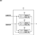
- FIG. 3 is a block diagram showing a configuration example of the flicker detection unit 21 of FIG.
- the flicker detection unit 21 includes inter-frame difference flicker detection units 31 and 32 and an inter-line difference flicker detection unit 33.
- the inter-frame difference flicker detection unit 31 obtains a difference between frames of an image constructed from the short accumulation signal supplied from the image sensor 12, thereby using a time change amount between frames and flickering the short accumulation signal. Detect if a component is included. As a result of the detection, the inter-frame difference flicker detection unit 31 obtains the amplitude and period of the flicker component of the short accumulation signal when it is detected that the short accumulation signal contains the flicker component. Then, the inter-frame difference flicker detection unit 31 supplies the flicker component amplitude of the short accumulation signal to the HDR synthesis processing unit 22 and supplies the cycle of the flicker component of the short accumulation signal to the imaging control unit 23.
- the inter-frame difference flicker detection unit 32 obtains a difference between frames of an image constructed from the long accumulation signal supplied from the image sensor 12, and uses the time change amount between frames to flicker the long accumulation signal. Detect if a component is included. As a result of the detection, the inter-frame difference flicker detection unit 32 obtains the amplitude and period of the flicker component of the long accumulation signal when it is detected that the flicker component is included in the long accumulation signal. Then, the inter-frame difference flicker detection unit 32 supplies the amplitude of the flicker component of the long accumulation signal to the HDR synthesis processing unit 22 and supplies the cycle of the flicker component of the long accumulation signal to the imaging control unit 23.
- the inter-line difference flicker detection unit 33 uses the amount of change for each row of the image in each of the images constructed from the short accumulation signal and the long accumulation signal supplied from the image sensor 12 to store the short accumulation signal and the long accumulation signal. It is detected whether or not a flicker component is included in each signal. As a result of the detection, for example, when it is detected that the short accumulation signal contains a flicker component, the inter-line difference flicker detection unit 33 obtains the amplitude and period of the flicker component of the short accumulation signal, The flicker component amplitude of the accumulated signal is supplied to the HDR synthesizing unit 22, and the cycle of the flicker component of the short accumulation signal is supplied to the imaging control unit 23.
- the inter-line difference flicker detection unit 33 obtains the amplitude and period of the flicker component of the long accumulation signal, for example, when it is detected that the long accumulation signal contains the flicker component, and flickers the long accumulation signal.
- the amplitude of the component is supplied to the HDR synthesis processing unit 22, and the cycle of the flicker component of the long accumulation signal is supplied to the imaging control unit 23.
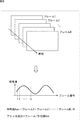
- the inter-frame difference flicker detection unit 31 sequentially images (frames 1, 2,..., Based on short accumulation signals supplied from the image sensor 12 as time passes. N).
- the inter-frame difference flicker detection unit 32 sequentially constructs images (frames 1, 2,..., N) based on the long accumulation signal supplied from the image sensor 12 as time elapses.
- the observed signal When flicker occurs in the image, when the brightness of the image for each frame is observed, the observed signal has a waveform as shown in the lower side of FIG. That is, if flicker occurs due to blinking of the light source, the observed signal in the image in which the subject is imaged is obtained by adding the flicker component to the subject's own brightness. Therefore, in order to obtain the flicker component, first, it is necessary to calculate the brightness unique to the subject.
- the influence of flicker can be eliminated by setting the number of frames used for calculating the average value Ave to a time proportional to the light source flicker cycle. With this method, if the subject is not moving, the subject's own brightness excluding the influence of flicker can be calculated.
- the inter-frame difference flicker detection units 31 and 32 calculate a flicker component in each frame from the brightness unique to the subject.
- the inter-frame difference flicker detection units 31 and 32 calculate the flicker component, and if the flicker component is equal to or greater than a certain threshold, it is determined that the short accumulation signal and the long accumulation signal include the flicker component. can do.
- the inter-frame difference flicker detection units 31 and 32 divide the observed signal (signal value) by the subject's own brightness to obtain a flicker component ratio (signal ratio). ) Is calculated.
- the inter-frame difference flicker detection units 31 and 32 approximate the calculated flicker ratio with an arbitrary sine wave, as shown on the lower side of FIG. Accordingly, the inter-frame difference flicker detection units 31 and 32 determine that flicker has occurred in the image if the amplitude of the sine wave (approximate waveform) obtained by approximation is equal to or greater than a predetermined threshold. If it cannot be approximated to any sine wave, it is assumed that the brightness varies due to factors other than flicker (for example, the subject has moved). In this case, it is detected as flicker. Not.
- the image sensor 12 is a CMOS (Complementary Metal Oxide Semiconductor) image sensor
- CMOS Complementary Metal Oxide Semiconductor
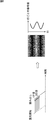
- a rolling shutter for sequentially reading out image signals is performed for each row of the image. Therefore, there is a time difference in the exposure timing between the uppermost row and the lowermost row. Therefore, as shown on the right side of FIG. 6, the CMOS image sensor has a characteristic that when the light source includes flicker, a phenomenon in which the brightness varies depending on the row occurs.
- the inter-line difference flicker detection unit 33 calculates the average value of each line in the image using such characteristics, and detects the flicker using the change amount of the average value.
- the integrated value of the image signal for each row may be used.
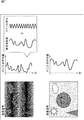
- the average value of the image signal when the average value of the image signal is calculated for each row and plotted in the row direction, the average value of the image signal includes the original brightness (subject brightness) and flicker component as shown in FIG. It is included.
- the original brightness of the subject is determined from the image signal whose exposure time is controlled. Can be sought.
- FIG. 7 shows an example in which the flicker component is not included in the image configured using the long accumulation signal.
- the inter-line difference flicker detection unit 33 can obtain the flicker component by calculating the signal ratio between the short accumulation signal and the long accumulation signal.
- the inter-line difference flicker detection unit 33 calculates the flicker component based on the signal ratio of the short accumulation signal and the long accumulation signal in a state where the flicker component is not included in the long accumulation signal, and the flicker component is constant. If it is equal to or greater than the threshold, it is detected that the flicker component is included in the short accumulation signal.
- the inter-line difference flicker detection unit 33 approximates the signal ratio of the flicker component with a sine wave, similarly to the inter-frame difference flicker detection units 31 and 32, and obtains the flicker component amplitude and period. Can be supplied to the HDR synthesis processing unit 22. That is, with the horizontal axis in FIG. 5 described above as the row coordinate, the amplitude and period of the flicker component included in one frame of the short accumulation signal can be obtained.
- the inter-line difference flicker detection unit 33 is configured so that the flicker included in one frame of the long accumulation signal is based on the signal ratio of the short accumulation signal and the long accumulation signal in a state where the flicker component is not included in the short accumulation signal.
- the amplitude and period of the component can be determined.
- flicker occurs in either one of the image configured using the short accumulation signal and the image configured using the long accumulation signal. It is assumed that it is not.
- an HDR image is configured using the short accumulation signal S, the long accumulation signal L, the black level B opb , the exposure ratio gain, and the blend ratio ⁇ as in the following equation (1).
- the signal HDR to be calculated is calculated.
- the blend ratio ⁇ between the short accumulation signal and the long accumulation signal is set so as to be switched according to the brightness of the subject.
- the signal HDR is calculated by calculating Expression (1).
- the blend ratio ⁇ uses a long accumulation signal that can be imaged up to a dark part by long exposure.
- the signal is set to be used. That is, when the brightness of the subject is equal to or less than the threshold value TH0, the blend ratio ⁇ is set to 0.
- the blend ratio ⁇ is set to 1, and the threshold value TH0 to the threshold value TH1. Then, the blend ratio ⁇ is changed linearly.
- the HDR synthesizing unit 22 switches the blend ratio ⁇ between the short accumulation signal and the long accumulation signal according to the flicker detection result by the flicker detection unit 21, that is, according to the magnitude of the amplitude A of the flicker component. Change the setting.
- the HDR synthesis processing unit 22 updates the threshold value TH0 and the threshold value TH1 based on the amplitude A of the flicker component according to the following equation (2).
- c0 and c1 are arbitrary coefficients proportional to the brightness of the subject.
- the threshold value TH0 and the threshold value TH1 are updated to a large value, and the long accumulation signal is often used. That is, the use of the short accumulation signal including the flicker component is reduced, and the HDR synthesis processing unit 22 can generate an HDR image in which flicker is suppressed.
- the HDR synthesis processing unit 22 updates the threshold value TH0 and the threshold value TH1 based on the amplitude A of the flicker component according to the following equation (3).
- d0 and d1 are arbitrary coefficients proportional to the brightness of the subject.
- the threshold value TH0 and the threshold value TH1 are updated to small values, and the short accumulation signal is often used. That is, the use of the long accumulation signal including the flicker component is reduced, and the HDR synthesis processing unit 22 can generate an HDR image in which flicker is suppressed.
- FIG. 9 shows general exposure time and analog gain control.
- the horizontal axis indicates the brightness of the subject
- the right vertical axis indicates the exposure time
- the left vertical axis indicates the analog gain.
- the exposure time and analog gain are controlled according to the brightness of the subject. That is, when the subject is very bright, the exposure time is set to a minimum unit (Min speed), and the analog gain is also set to a minimum value (Min Gain). Then, as the subject becomes darker, the exposure time is first controlled to gradually increase, and after the exposure time reaches the longest (1/60), the analog gain is controlled to increase.
- Min speed minimum unit
- Min Gain minimum value
- the brightness of the subject is determined by the histogram of the captured image as shown in FIG.
- the horizontal axis indicates the brightness
- the vertical axis indicates the histogram value.
- the imaging control unit 23 calculates the exposure level by summing up the product of the histogram value and the signal value, and determines that the exposure is insufficient when the value is darker than the preset brightness of the target. Control to increase the exposure time or analog gain.
- AE Automatic Exposure
- the imaging control unit 23 first selects an image configured using the short accumulation signal and an image configured using the long accumulation signal. Calculate the histogram.
- the image is clipped to 1023 and acquired for an image configured using a short accumulation signal. Calculate by dividing. Thereafter, the imaging control unit 23 adjusts the exposure level of each image. At this time, the exposure level target can be set to a different value between the short accumulation signal and the long accumulation signal.
- the imaging control unit 23 controls the exposure time based on the cycle of the flicker component supplied from the flicker detection unit 21, as shown in FIG. Do.
- FIG. 12 shows the relationship between the brightness of the subject and the exposure time.
- the thick line represents the exposure time control when flicker correction is not performed
- the thin line is the exposure time when flicker correction is performed. Represents the control.
- the minimum flickerless exposure time is set to a half cycle T of the brightness of the light source (flicker component).
- the exposure time is a half cycle T of the brightness cycle of the light source, it is possible to avoid being affected by flicker regardless of the timing of imaging.
- the half cycle T is set to 8.333 milliseconds.
- the imaging control unit 23 controls at least one of the short accumulation signal and the long accumulation signal in which the flicker component is detected to be a constant multiple of the minimum flickerless exposure time.
- the occurrence of flicker is suppressed in the image.
- the exposure time is controlled so as to be a constant multiple of the minimum flickerless exposure time (2 times, 4 times, 6 times, etc.)
- an arbitrary exposure ratio cannot be set, and the exposure ratio is It is limited to an integral multiple (for example, 1 ⁇ , 2 ⁇ , 3 ⁇ , 8 ⁇ , etc.). Therefore, the imaging control unit 23 increases the analog gain of the image signal for which the exposure time is controlled in accordance with the exposure ratio that is insufficient by controlling the exposure time, so that an arbitrary exposure ratio is obtained. Can be adjusted.
- the image processing apparatus 11 can generate flicker-free HDR images by suppressing the occurrence of flicker when capturing HDR images. Further, since the image processing apparatus 11 only controls the exposure time of the image sensor 12 and the blend ratio ⁇ when generating the HDR image, for example, the image processing is performed on the image itself based on the detected flicker. It is possible to avoid the occurrence of side effects such as overcorrection compared to the correction method that is performed.
- FIG. 14 is a block diagram illustrating a configuration example of the second embodiment of the image processing apparatus to which the present technology is applied.
- the same reference numerals are given to components common to the image processing apparatus 11 in FIG. 1, and detailed description thereof is omitted. That is, the image processing apparatus 11A has the same configuration as the image processing apparatus 11 of FIG. 1 in that it includes a flicker detection unit 21, an HDR synthesis processing unit 22, an imaging control unit 23, and a camera signal processing unit 24.
- the image processing apparatus 11A is different from the image processing apparatus 11 in FIG. 1 in that it includes a flicker correction unit 25.
- the flicker correction unit 25 is provided in the previous stage of the HDR synthesizing unit 22, and the short accumulation signal and the long accumulation signal are reduced so that the flicker component included in the short accumulation signal and the long accumulation signal output from the image sensor 12 is reduced. Correct. For example, when the flicker detection unit 21 detects that a short accumulation signal or a long accumulation signal contains a flicker component, the flicker component is approximated by a sine wave as described above, and the cycle and amplitude of the sine wave are calculated. The flicker correction unit 25 is supplied. As a result, the flicker correction unit 25 reduces the flicker component by correcting the signal value of the short accumulation signal or the long accumulation signal containing the flicker component with the sine wave supplied from the flicker detection unit 21. Then, the corrected short accumulation signal or long accumulation signal is supplied to the HDR synthesis processing unit 22.
- an HDR image in which the occurrence of flicker is suppressed can be generated in the same manner as the image processing apparatus 11 in FIG.
- FIG. 15 is a block diagram illustrating a configuration example of the third embodiment of the image processing apparatus to which the present technology is applied.
- the same reference numerals are given to the same components as those in the image processing apparatus 11 in FIG. 1, and detailed description thereof will be omitted. That is, the image processing apparatus 11B has the same configuration as that of the image processing apparatus 11 of FIG. 1 in that it includes an imaging control unit 23 and a camera signal processing unit 24.
- the flicker detection unit 21B and the HDR synthesis processing unit 22B can perform processing on signals exposed with four different exposure times. It is configured.
- the short accumulation signals 1 to 3 and the long accumulation signal exposed at four different exposure times are output from the image sensor 12, and are supplied to the flicker detection unit 21B and the HDR synthesis processing unit 22B, respectively.
- the flicker detection unit 21B detects whether or not a flicker component is included from each of the short accumulation signals 1 to 3 and the long accumulation signal.
- the HDR synthesis processing unit 22B can generate an HDR image with a wider dynamic range using the short accumulation signals 1 to 3 and the long accumulation signal.
- the image processing apparatus 11B can suppress flicker occurring in the HDR image generated from the short accumulation signals 1 to 3 and the long accumulation signal exposed at four different exposure times.
- the present technology performs processing on image signals exposed at two different types of exposure times as in the image processing apparatus 11 of FIG. 1 and four types of different exposure times as in the image processing apparatus 11B of FIG.
- the present invention can be applied to processing on an image signal exposed with a plurality of different types of exposure times.
- FIG. 16 is a block diagram showing a modification of the flicker detection unit 21.
- the flicker detection unit 21C includes inter-frame difference flicker detection units 31 and 32. That is, the flicker detection unit 21 in FIG. 3 includes the inter-line difference flicker detection unit 33, whereas the flicker detection unit 21C does not include the inter-line difference flicker detection unit 33.
- the flicker detection unit 21C includes only the inter-frame difference flicker detection units 31 and 32, as described above, it is possible to detect flicker using the amount of time change between frames. That is, the inter-line difference flicker detection unit 33 is not an essential component for detecting flicker. Further, the flicker may be detected only by the inter-line difference flicker detection unit 33. That is, as long as the flicker component contained in the short accumulation signal and the long accumulation signal can be detected, the configuration is not limited to the configuration of the flicker detection unit 21 or the flicker detection unit 21C.
- the image processing apparatus 11 of each embodiment as described above is, for example, an imaging system such as a digital still camera or a digital video camera, a mobile phone having an imaging function, or another device having an imaging function. It can be applied to various electronic devices.
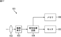
- FIG. 17 is a block diagram illustrating a configuration example of an imaging device mounted on an electronic device.
- the imaging apparatus 101 includes an optical system 102, an imaging element 103, a signal processing circuit 104, a monitor 105, and a memory 106, and can capture still images and moving images.
- the optical system 102 includes one or more lenses, guides image light (incident light) from a subject to the image sensor 103, and forms an image on a light receiving surface (sensor unit) of the image sensor 103.
- the image sensor 103 corresponds to the image sensor 12 described above.
- electrons are accumulated for a certain period according to an image formed on the light receiving surface via the optical system 102. Then, a signal corresponding to the electrons accumulated in the image sensor 103 is supplied to the signal processing circuit 104.
- the signal processing circuit 104 can apply the above-described image processing apparatus 11 as part of its function, and performs various signal processing on the image signal output from the image sensor 103.
- An image (image data) obtained by performing signal processing by the signal processing circuit 104 is supplied to the monitor 105 and displayed, or supplied to the memory 106 and stored (recorded).
- the occurrence of flicker at the time of capturing an HDR image is suppressed by applying the image processing apparatus 11 according to each of the above-described embodiments. For example, a higher-quality HDR image is generated. An image can be taken.
- this technique can also take the following structures.
- a flicker detection unit that obtains at least the amplitude of the flicker component from the image signal including flicker components caused by flickering of a light source among a plurality of image signals captured at a plurality of types of exposure times;
- a blending processing unit configured to change a blend rate when the plurality of image signals are combined according to the amplitude of the flicker component obtained by the flicker detection unit, and to combine the plurality of image signals according to the blend rate.
- An image processing apparatus (2) The flicker detection unit determines whether or not the flicker component is included in each of the plurality of image signals based on a temporal change amount between the frames for each image composed of the plurality of image signals.
- the image processing apparatus detects and obtains at least an amplitude of the flicker component from the image signal including the flicker component. (3) Whether the flicker detection unit includes the flicker component in each of the plurality of image signals based on the amount of change for each row of each image in each image of one frame composed of each of the plurality of image signals.
- the image processing apparatus detects whether or not and obtains at least an amplitude of the flicker component from the image signal including the flicker component.
- the flicker detection unit further obtains a cycle of the flicker component, From the above (1) to (3), further comprising: an imaging control unit that performs control to change an exposure time of the image signal including the flicker component according to the cycle of the flicker component obtained by the flicker detection unit An image processing apparatus according to any one of the above.
- the imaging control unit performs control to increase an analog gain of the image signal according to an insufficient exposure ratio by setting the exposure time of the image signal including the flicker component (4) Or the image processing apparatus as described in (5).
- the flicker detection unit and the composition processing unit are supplied with a short exposure image signal obtained from a pixel that performs short exposure and a long exposure image signal obtained from a pixel that performs long exposure,
- the imaging control unit determines an exposure time of the image signal in which the flicker component is detected by the flicker detection unit of the short-time exposure image signal and the long-time exposure image signal as a half cycle of the flicker component period.
- the image processing device according to any one of (4) to (6).
- the flicker detection unit obtains the original brightness of the subject from the image signal whose exposure time is controlled after the exposure time is controlled by the imaging control unit.
- the flicker detection unit When detecting the flicker component from the image signal whose exposure time is not controlled by the imaging control unit, the flicker detection unit obtains the amplitude of the flicker component and supplies the amplitude of the flicker component to the synthesis processing unit.
- the image processing apparatus according to any one of (4) to (8).
Landscapes
- Engineering & Computer Science (AREA)
- Multimedia (AREA)
- Signal Processing (AREA)
- Physics & Mathematics (AREA)
- General Physics & Mathematics (AREA)
- Studio Devices (AREA)
- Exposure Control For Cameras (AREA)
Abstract
本開示は、HDR撮像時におけるフリッカの影響を低減することができるようにする画像処理装置および画像処理方法、並びにプログラムに関する。 フリッカ検出部は、短時間露光を行う画素から得られた短時間露光画像信号、および、長時間露光を行う画素から得られた長時間露光画像信号のうち、光源のちらつきによるフリッカ成分が含まれている画像信号からフリッカ成分の振幅および周期を求める。そして、合成処理部は、フリッカ成分の振幅に従って、短時間露光画像信号および長時間露光画像信号を合成する際のブレンド率を変更し、そのブレンド率に応じて短時間露光画像信号および長時間露光画像信号を合成する。さらに、撮像制御部は、フリッカ成分の周期に従って、フリッカ成分が含まれている画像信号の露光時間を変更する制御を行う。本技術は、例えば、HDR画像を撮像可能な撮像装置に適用できる。
Description
本開示は、画像処理装置および画像処理方法、並びにプログラムに関し、特に、HDR撮像時におけるフリッカの影響を低減することができるようにした画像処理装置および画像処理方法、並びにプログラムに関する。
一般的に、光源がちらついている環境で撮像が行われると、画像にフリッカ(光点滅)が発生することがある。
従来より、フリッカを補正する技術が開発されている。例えば、最も多く利用されている手法の一つとして、光源のフリッカが発生している事を検出し、そのフリッカ周波数に応じて、撮像素子の露光時間を変更する手法がある(特許文献1参照)。具体的には、光源のフリッカの半周期時間をTとしたとき、撮像素子の露光時間を半周期時間Tの定数倍に設定する(露光時間=a×T:aは任意の自然数)。これにより、各フレームにおける光源の入射量を常に一定に保つことができ、光源フリッカの影響を排除することができる。
また、近年、HDR(High Dynamic Range:ハイダイナミックレンジ)画像を撮像するための技術として、複数種類の露光時間で撮像された画像信号を組み合わせる撮像手法が利用されている。
ところで、HDR画像を撮像する際において、上述したようなフリッカ補正が上手く機能しないことがあった。つまり、HDR画像の撮像時には、特に短露光画素において、露光時間を十分短く設定し、適正露光時間では飽和してしまう明るい領域を撮像する必要がある。そのため、短露光画素の露光時間をフリッカ光源の半周期に比例するように設定(露光時間=a×T)することができない場合が多く、そのような場合には光源のフリッカを補正することができなかった。
一方、フリッカ成分の含まれない基準画像を生成し、その基準画像との差分を用いてフリッカを含む画像を補正する手法が提案されている(特許文献2参照)。しかしながら、このような手法では動被写体などによってフリッカを誤検出することがあり、過補正などの副作用が発生する可能性があった。
上述したように、従来、HDR撮像時においてフリッカを適切に補正することは困難であり、HDR撮像時におけるフリッカの影響を低減することが求められている。
本開示は、このような状況に鑑みてなされたものであり、HDR撮像時におけるフリッカの影響を低減することができるようにするものである。
本開示の一側面の画像処理装置は、複数種類の露光時間で撮像された複数の画像信号のうち、光源のちらつきによるフリッカ成分が含まれている前記画像信号から前記フリッカ成分の振幅を少なくとも求めるフリッカ検出部と、前記フリッカ検出部により求められた前記フリッカ成分の振幅に従って、複数の前記画像信号を合成する際のブレンド率を変更し、そのブレンド率に応じて複数の前記画像信号を合成する合成処理部とを備える。
本開示の一側面の画像処理方法またはプログラムは、複数種類の露光時間で撮像された複数の画像信号のうち、光源のちらつきによるフリッカ成分が含まれている前記画像信号から前記フリッカ成分の振幅を少なくとも求め、求められた前記フリッカ成分の振幅に従って、複数の前記画像信号を合成する際のブレンド率を変更し、そのブレンド率に応じて複数の前記画像信号を合成するステップを含む。
本開示の一側面においては、複数種類の露光時間で撮像された複数の画像信号のうち、光源のちらつきによるフリッカ成分が含まれている画像信号からフリッカ成分の振幅が少なくとも求められる。そして、求められたフリッカ成分の振幅に従って、複数の画像信号を合成する際のブレンド率が変更されて、そのブレンド率に応じて複数の画像信号が合成される。
本開示の一側面によれば、HDR撮像時におけるフリッカの影響を低減することができる。
以下、本技術を適用した具体的な実施の形態について、図面を参照しながら詳細に説明する。
図1は、本技術を適用した画像処理装置の第1の実施の形態の構成例を示すブロック図である。
図1に示す画像処理装置11は、撮像素子12により撮像された画像に対する画像処理を行い、図示しない後段の回路に出力する。例えば、撮像素子12は、短時間露光を行って発生する電荷を蓄積する短時間露光蓄積画素から得られた画像信号である短蓄信号(短時間露光画像信号)と、長時間露光を行って発生する電荷を蓄積する長時間露光蓄積画素から得られた画像信号である長蓄信号(長時間露光画像信号)とを出力する。そして、画像処理装置11は、明るさに応じたブレンド率(使用比率)で短蓄信号および長蓄信号を合成して、ダイナミックレンジの広いHDR画像を生成する画像処理を行う。
図1に示すように、画像処理装置11は、フリッカ検出部21、HDR合成処理部22、撮像制御部23、およびカメラ信号処理部24を備えて構成される。
フリッカ検出部21は、撮像素子12から出力される短蓄信号および長蓄信号を取得して、短蓄信号および長蓄信号を観測することにより、短蓄信号または長蓄信号に光源のフリッカ成分が含まれているかどうかを検出する。即ち、フリッカ検出部21は、短蓄信号から構成される画像および長蓄信号から構成される画像のいずれかにフリッカが発生しているか否かを検出するフリッカの検出処理を行う。そして、フリッカ検出部21は、フリッカが発生していたことが検出された場合には、短蓄信号または長蓄信号に含まれているフリッカ成分の振幅および周期を求め、フリッカ成分の振幅をHDR合成処理部22に供給し、フリッカ成分の周期を撮像制御部23に供給する。なお、フリッカ検出部21による処理については、図3乃至図7を参照して後述する。
HDR合成処理部22は、フリッカ検出部21から供給されるフリッカ成分の振幅に応じて、図8を参照して後述するように、HDR合成処理を行う際の短蓄信号と長蓄信号とのブレンド率を適応的に変更する。そして、HDR合成処理部22は、適応的に変更されたブレンド率で短蓄信号および長蓄信号を合成することによりHDR画像を生成し、撮像制御部23およびカメラ信号処理部24に供給する。
撮像制御部23は、HDR合成処理部22から供給されるHDR画像の明るさに基づいて、撮像素子12により適切な明るさの画像が撮像されるように、撮像素子12の露光時間およびアナログゲインを制御する。このとき、撮像制御部23は、フリッカ検出部21から供給されるフリッカ成分の周期に従って、フリッカ成分が含まれている方の画像信号(短蓄信号および長蓄信号の一方)の露光時間を変更する制御を行う。即ち、撮像制御部23は、図12を参照して後述するように、フリッカの影響を抑制することができる最小の露光時間である最小フリッカレス露光時間の定数倍となるように、撮像素子12の露光時間を制御する。
カメラ信号処理部24は、HDR合成処理部22から供給されるHDR画像に対する一般的な画像処理を行い、例えば、ガンマ補正やホワイトバランス調整などを行い、図示しない後段の回路に供給する。
このように構成される画像処理装置11では、フリッカ検出部21によりフリッカが発生していることが検出されると、HDR合成処理部22においてブレンド率が適応的に変更されるとともに、撮像制御部23において撮像素子12の露光時間が制御される。これにより、短蓄信号および長蓄信号に含まれるフリッカ成分を低減することができ、HDR画像におけるフリッカの影響を抑制することができる。
次に、図2は、画像処理装置11において行われる画像処理を説明するフローチャートである。
例えば、撮像素子12が撮像を開始して短蓄信号および長蓄信号の出力を行うと処理が開始され、ステップS11において、フリッカ検出部21およびHDR合成処理部22は、1フレーム分(時刻t)の短蓄信号および長蓄信号をそれぞれ取得する。
ステップS12において、フリッカ検出部21は、ステップS11で取得した1フレーム分の短蓄信号および長蓄信号に基づいて、短蓄信号または長蓄信号に光源のフリッカ成分が含まれているかどうかを検出するフリッカの検出処理を行う。
ステップS13において、HDR合成処理部22は、ステップS11で取得した1フレーム分の短蓄信号および長蓄信号を、所定のブレンド率(例えば、明るさに応じた設定値)で合成することにより、HDR画像を生成する。そして、HDR合成処理部22は、生成したHDR画像を、撮像制御部23およびカメラ信号処理部24に供給する。なお、このフレームに対しては、HDR合成処理部22は、直前のステップS12においてフリッカ検出部21により検出されたフリッカに対する処理は行わず、そのままHDR画像を出力する。
ステップS14において、フリッカ検出部21は、ステップS12でフリッカの検出処理を行った結果、フリッカが発生していたか否かを判定する。
ステップS14において、フリッカが発生していなかったと判定された場合、処理はステップS11に戻り、以下、同様の処理が繰り返される。一方、ステップS14において、フリッカが発生していたと判定された場合、処理はステップS15に進む。
ステップS15において、フリッカ検出部21は、ステップS12で検出されたフリッカ成分の周期を求めて撮像制御部23に供給し、撮像制御部23は、そのフリッカの周期に従って撮像素子12の露光時間を調整する。例えば、長蓄信号にフリッカ成分が含まれていた場合、撮像素子12は、長時間露光蓄積画素の露光時間が最小フリッカレス露光時間(図12参照)の定数倍となるような調整を行う。
ステップS16において、フリッカ検出部21およびHDR合成処理部22は、ステップS11で取得したフレームの次の1フレーム分(時刻t+1)の短蓄信号および長蓄信号をそれぞれ取得する。
ステップS17において、フリッカ検出部21は、ステップS16で取得した1フレーム分の短蓄信号および長蓄信号に基づいて、短蓄信号または長蓄信号に光源のフリッカ成分が含まれているかどうかを検出するフリッカの検出処理を行う。
ステップS18において、フリッカ検出部21は、ステップS17でフリッカの検出処理を行った結果、フリッカが発生していたか否かを判定する。
ステップS18において、フリッカが発生していなかったと判定された場合、処理はステップS11に戻り、以下、同様の処理が繰り返される。一方、ステップS18において、フリッカが発生していたと判定された場合、処理はステップS19に進む。
ステップS19において、フリッカ検出部21は、ステップS17で検出されたフリッカ成分の振幅を求めてHDR合成処理部22に供給し、HDR合成処理部22は、そのフリッカ成分の振幅に基づいて、ブレンド率を適応的に変更する。例えば、ステップS15において、長時間露光蓄積画素の露光時間が最小フリッカレス露光時間の定数倍となるような調整が行われていれば、ステップS17のフリッカの検出処理では、短蓄信号に含まれているフリッカ成分が検出されることになる。従って、フリッカ検出部21は、短蓄信号のフリッカ成分の振幅をHDR合成処理部22に供給し、HDR合成処理部22は、短蓄信号の使用比率を低減するように(図8参照)、ブレンド率を変更する。
ステップS20において、HDR合成処理部22は、ステップS16で取得した1フレーム分の短蓄信号および長蓄信号を、ステップS19で変更したブレンド率で合成することにより、HDR画像を生成し、撮像制御部23およびカメラ信号処理部24に供給する。そして、ステップS20の処理後、処理はステップS11に戻り、以下、同様の処理が繰り返される。
次に、図3は、図1のフリッカ検出部21の構成例を示すブロック図である。
図3に示すように、フリッカ検出部21は、フレーム間差分フリッカ検出部31および32、並びに、ライン間差分フリッカ検出部33を備えて構成される。
フレーム間差分フリッカ検出部31は、撮像素子12から供給される短蓄信号から構築される画像のフレームどうしの差分を求めることによって、フレーム間の時間変化量を利用して、短蓄信号にフリッカ成分が含まれているかどうかを検出する。その検出を行った結果、フレーム間差分フリッカ検出部31は、短蓄信号にフリッカ成分が含まれていることが検出された場合、短蓄信号のフリッカ成分の振幅および周期を求める。そして、フレーム間差分フリッカ検出部31は、短蓄信号のフリッカ成分の振幅をHDR合成処理部22に供給し、短蓄信号のフリッカ成分の周期を撮像制御部23に供給する。
フレーム間差分フリッカ検出部32は、撮像素子12から供給される長蓄信号から構築される画像のフレームどうしの差分を求めることによって、フレーム間の時間変化量を利用して、長蓄信号にフリッカ成分が含まれているかどうかを検出する。その検出を行った結果、フレーム間差分フリッカ検出部32は、長蓄信号にフリッカ成分が含まれていることが検出された場合、長蓄信号のフリッカ成分の振幅および周期を求める。そして、フレーム間差分フリッカ検出部32は、長蓄信号のフリッカ成分の振幅をHDR合成処理部22に供給し、長蓄信号のフリッカ成分の周期を撮像制御部23に供給する。
ライン間差分フリッカ検出部33には、撮像素子12から供給される短蓄信号および長蓄信号から構築される画像それぞれにおいて、画像の行ごとの変化量を利用して、短蓄信号および長蓄信号それぞれにフリッカ成分が含まれているかどうかを検出する。その検出を行った結果、ライン間差分フリッカ検出部33は、例えば、短蓄信号にフリッカ成分が含まれていることが検出された場合、短蓄信号のフリッカ成分の振幅および周期を求め、短蓄信号のフリッカ成分の振幅をHDR合成処理部22に供給し、短蓄信号のフリッカ成分の周期を撮像制御部23に供給する。同様に、ライン間差分フリッカ検出部33は、例えば、長蓄信号にフリッカ成分が含まれていることが検出された場合、長蓄信号のフリッカ成分の振幅および周期を求め、長蓄信号のフリッカ成分の振幅をHDR合成処理部22に供給し、長蓄信号のフリッカ成分の周期を撮像制御部23に供給する。
ここで、図4および図5を参照して、フレーム間差分フリッカ検出部31および32が、フレーム間の時間変化量を利用してフリッカを検出する手法について説明する。
例えば、フレーム間差分フリッカ検出部31は、図4の上側に示すように、時刻の経過に従って順次、撮像素子12から供給される短蓄信号に基づいた画像(フレーム1,2,・・・,N)を構築する。同様に、フレーム間差分フリッカ検出部32は、時刻の経過に従って順次、撮像素子12から供給される長蓄信号に基づいた画像(フレーム1,2,・・・,N)を構築する。
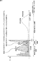
そして、画像にフリッカが発生している場合には、フレームごとの画像の明るさを観測すると、その観測された信号は、図4の下側に示すような波形となる。即ち、光源が点滅することによりフリッカが発生していると、被写体が撮像されている画像において、観測された信号は、被写体独自の明るさにフリッカ成分が加算されたものとなる。従って、フリッカ成分を求めるには、まず、被写体独自の明るさを算出する必要がある。
そこで、フレーム間差分フリッカ検出部31および32は、複数のフレーム数の被写体の明るさを積算し、その平均値Ave(=(フレーム1+フレーム2+・・・+フレームN)/N)を、被写体独自の明るさとして算出する。ここで、平均値Aveの算出に使用するフレーム数を、光源フリッカの周期に比例する時間に設定することで、フリッカの影響を排除することができる。この手法により、被写体が動いていなければ、フリッカの影響を排除した被写体独自の明るさを算出することができる。
次に、フレーム間差分フリッカ検出部31および32は、被写体独自の明るさから、各フレームにおけるフリッカ成分を算出する。例えば、フレーム間差分フリッカ検出部31および32は、各フレームの信号を、被写体独自の明るさで除算することによりフリッカ成分(=フレーム/平均値Ave)を求めることができる。即ち、平均値Aveとの比が大きい部分がフリッカ成分となる。
このように、フレーム間差分フリッカ検出部31および32は、フリッカ成分を算出し、そのフリッカ成分が一定の閾値以上であれば、短蓄信号および長蓄信号にフリッカ成分が含まれていると判断することができる。
例えば、図5の上側に示すように、フレーム間差分フリッカ検出部31および32は、観測された信号(信号値)を、被写体独自の明るさで除算することによって、フリッカ成分の比率(信号比)を算出する。
そして、フレーム間差分フリッカ検出部31および32は、図5の下側に示すように、算出したフリッカ比率を任意のサイン波で近似する。これにより、フレーム間差分フリッカ検出部31および32は、近似により得られたサイン波(近似波形)の振幅が、所定の閾値以上であれば、画像にフリッカが発生していると判断する。なお、どのようなサイン波にも近似することができない場合には、フリッカ以外の要因による明るさの変動(例えば、被写体が動いたなど)であると想定され、この場合には、フリッカとして検出されない。
ところで、フレーム間の時間変化量を利用してフリッカを検出する手法では、複数のフレームの平均値Aveを算出する際に、被写体または撮像装置が移動していた場合には、その移動によって明るさが変化してしまい、フリッカを正確に検出することは困難である。そこで、1つのフレームの信号のみでフリッカ成分を求めることで、そのような明るさの変化による影響を排除することができる。
次に、図6および図7を参照して、ライン間差分フリッカ検出部33が、画像の行ごとの変化量を利用してフリッカを検出する手法について説明する。
図6の左側に示すように、撮像素子12がCMOS(Complementary Metal Oxide Semiconductor)イメージセンサである場合には、画像の各行ごとに順次、画像信号を読み出すローリングシャッターが行われる。従って、最上段の行と最下段の行とでは、露光するタイミングに時間差が生じることになる。そのため、CMOSイメージセンサは、図6の右側に示すように、光源にフリッカが含まれている場合、行ことに明るさが異なる現象が発生する特性を有する。
そこで、ライン間差分フリッカ検出部33は、このような特性を利用して、画像における各行の平均値を算出することで、それらの平均値の変化量を利用してフリッカの検出を行う。なお、行ごとの画像信号の平均値を用いる他、行ごとの画像信号の積算値を用いてもよい。
例えば、行ごとに画像信号の平均値を算出し、それらを行方向にプロットすると、図7に示すように、画像信号の平均値には、被写体本来の明るさ(被写体明度)と、フリッカ成分が含まれている。ここで、短蓄信号および長蓄信号のいずれか一方においてフリッカが発生しないように露光時間を制御(図12参照)した後に、露光時間が制御された方の画像信号から被写体本来の明るさを求めることができる。
図7には、長蓄信号を用いて構成される画像においてフリッカ成分が含まれていない例が示されている。この場合、ライン間差分フリッカ検出部33は、短蓄信号および長蓄信号の信号比を算出することで、フリッカ成分を求めることができる。
例えば、ライン間差分フリッカ検出部33は、長蓄信号にフリッカ成分が含まれないような状態で短蓄信号および長蓄信号の信号比に基づいてフリッカ成分を算出し、そのフリッカ成分が一定の閾値以上であれば、短蓄信号にフリッカ成分が含まれているとして検出する。そして、ライン間差分フリッカ検出部33は、フリッカを検出すると、フレーム間差分フリッカ検出部31および32と同様に、フリッカ成分の信号比をサイン波で近似して、フリッカ成分の振幅および周期を求めてHDR合成処理部22に供給することができる。即ち、上述した図5における横軸を行の座標として、1フレームの短蓄信号に含まれるフリッカ成分の振幅および周期を求めることができる。
同様に、ライン間差分フリッカ検出部33は、短蓄信号にフリッカ成分が含まれないような状態で短蓄信号および長蓄信号の信号比に基づいて、1フレームの長蓄信号に含まれるフリッカ成分の振幅および周期を求めることができる。即ち、ライン間差分フリッカ検出部33がフリッカを検出するためには、短蓄信号を用いて構成される画像、および、長蓄信号を用いて構成される画像のいずれか一方に、フリッカが発生していない状態とされる。
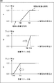
次に、図8を参照して、HDR合成処理部22におけるHDR合成処理について説明する。
まず、通常のHDR合成処理では、次の式(1)のように、短蓄信号S、長蓄信号L、黒レベルBopb、露光比gain、およびブレンド比αを用いて、HDR画像を構成する信号HDRが演算される。

そして、図8のAに示すように、短蓄信号と長蓄信号とのブレンド比αが、被写体の明るさに応じて切り替えられるように設定されており、このようなブレンド比αを用いて式(1)を演算することで、信号HDRが算出される。一般的に、ブレンド比αは、被写体の明るさが暗い場合には、長時間露光により暗部まで撮像できる長蓄信号を用い、被写体の明るさが明るい場合には、明るくても飽和しない短蓄信号を用いるように設定されている。つまり、被写体の明るさが閾値TH0以下である場合にはブレンド比αを0とし、被写体の明るさが閾値TH1以上である場合にはブレンド比αを1として、閾値TH0から閾値TH1までの間ではブレンド比αを線形的に変化させる。
そして、HDR合成処理部22は、フリッカ検出部21によるフリッカの検出結果に応じて、即ち、フリッカ成分の振幅Aの大きさに応じて、短蓄信号と長蓄信号とのブレンド比αを切り替える設定を変更する。
例えば、HDR合成処理部22は、短蓄信号にフリッカ成分が含まれている場合には、次の式(2)に従って、フリッカ成分の振幅Aに基づいて、閾値TH0および閾値TH1を更新する。なお、式(2)において、c0およびc1は、被写体の明るさに比例する任意の係数である。

従って、図8のBに示すように、短蓄信号にフリッカ成分が含まれている時、閾値TH0および閾値TH1は大きな値に更新され、長蓄信号が多く使用されるようになる。即ち、フリッカ成分が含まれている短蓄信号の使用が減少することになり、HDR合成処理部22は、フリッカを抑制したHDR画像を生成することができる。
一方、HDR合成処理部22は、長蓄信号にフリッカ成分が含まれている場合には、次の式(3)に従って、フリッカ成分の振幅Aに基づいて、閾値TH0および閾値TH1を更新する。なお、式(3)において、d0およびd1は、被写体の明るさに比例する任意の係数である。

従って、図8のCに示すように、長蓄信号にフリッカ成分が含まれている時、閾値TH0および閾値TH1は小さな値に更新され、短蓄信号が多く使用されるようになる。即ち、フリッカ成分が含まれている長蓄信号の使用が減少することになり、HDR合成処理部22は、フリッカを抑制したHDR画像を生成することができる。
次に、図9乃至図13を参照して、撮像制御部23による撮像素子12の露光時間およびアナログゲインの制御について説明する。
図9には、一般的な露光時間およびアナログゲインの制御が示されている。図9において、横軸は被写体の明るさを示しており、右側の縦軸は露光時間を示し、左側の縦軸はアナログゲインを示している。
図9に示すように、被写体の明るさに応じて露光時間およびアナログゲインが制御される。即ち、被写体が非常に明るい場合には、露光時間は最小単位(Min speed)まで短く設定され、アナログゲインも最小値(Min Gain)に設定される。そして、被写体が暗くなるのに従って、まず、露光時間が徐々に長くなるように制御され、露光時間が最長(1/60)になった後、アナログゲインが増加するように制御される。
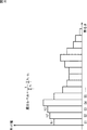
被写体の明るさは、図10に示すような撮像画像のヒストグラムによって判別される。図10において、横軸は明るさを示しており、縦軸はヒストグラム値を示している。
例えば、撮像制御部23は、ヒストグラム値および信号値の積を総和して露光レベルを算出し、その値が、予め設定されているターゲットの明るさよりも暗かった場合には、露光不足と判断して露光時間またはアナログゲインを増加するような制御を行う。
また、HDR画像におけるAE(Automatic Exposure)遷移も同様に行われ、撮像制御部23は、まず、短蓄信号を用いて構成される画像、および、長蓄信号を用いて構成される画像それぞれのヒストグラムを算出する。
例えば、図11に示すように、長蓄信号を用いて構成される画像については、画像を1023にクリップして取得し、短蓄信号を用いて構成される画像については、画像を露光比で除算して算出する。その後、撮像制御部23は、それぞれの画像の露光レベルを調整する。このとき、露光レベルのターゲットは、短蓄信号と長蓄信号とで異なる値に設定することができる。
ここで、撮像制御部23は、フリッカ検出部21によりフリッカが検出された場合には、フリッカ検出部21から供給されるフリッカ成分の周期に基づいて、図12に示すように露光時間の制御を行う。
図12には、被写体の明るさと露光時間との関係が示されており、太線が、フリッカ補正を行わない場合の露光時間の制御を表しており、細線が、フリッカ補正を行う場合の露光時間の制御を表している。
図12に示すように、フリッカ補正を行わない場合には直線的に露光時間が制御されるのに対して、フリッカ補正を行う場合には、最小フリッカレス露光時間の定数倍(2倍、4倍、6倍など)となるように露光時間が制御される。
ここで、最小フリッカレス露光時間は、図13に示すように、光源の明るさ(フリッカ成分)の周期の半周期Tに設定される。即ち、露光時間が光源の明るさの周期の半周期Tであれば、どのタイミングで撮像を行っても、フリッカの影響を受けることを回避することができる。具体的には、光源の明るさの周期が60Hzである場合、半周期Tは8.333ミリ秒に設定される。
このように、撮像制御部23は、短蓄信号および長蓄信号のうちフリッカ成分が検出された方の露光時間を、最小フリッカレス露光時間の定数倍となるように制御することで、少なくとも一方の画像にフリッカが発生することが抑制される。これにより、上述の図7を参照して説明したように、フリッカが発生していない画像に基づいて被写体本来の明るさを得ることができる。
なお、最小フリッカレス露光時間の定数倍(2倍、4倍、6倍など)となるように露光時間が制御される場合には、任意の露光比を設定することができなくなり、露光比が整数倍(例えば、1倍、2倍、3倍、8倍など)限定されることになる。そこで、撮像制御部23は、露光時間を制御することにより不足する露光比分に応じて、露光時間の制御を行った方の画像信号のアナログゲインを増加することで、任意の露光比となるように調整することができる。
以上のように、画像処理装置11では、HDR画像を撮像する際に、フリッカの発生を抑制し、ちらつきのないHDR画像を生成することができる。また、画像処理装置11は、撮像素子12の露光時間の制御、および、HDR画像を生成する際のブレンド比αを制御するだけなので、例えば、検出されたフリッカに基づいて画像そのものに対する画像処理を行うような補正方法と比較して、過補正などの副作用が発生することを回避することができる。
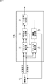
次に、図14は、本技術を適用した画像処理装置の第2の実施の形態の構成例を示すブロック図である。
図14に示す画像処理装置11Aにおいて、図1の画像処理装置11と共通する構成については同一の符号を付し、その詳細な説明は省略する。即ち、画像処理装置11Aは、フリッカ検出部21、HDR合成処理部22、撮像制御部23、およびカメラ信号処理部24を備える点で、図1の画像処理装置11と共通の構成とされる。
そして、画像処理装置11Aは、フリッカ補正部25を備える点で、図1の画像処理装置11と異なる構成となっている。
フリッカ補正部25は、HDR合成処理部22の前段に設けられ、撮像素子12から出力される短蓄信号および長蓄信号に含まれるフリッカ成分が低減されるように、短蓄信号および長蓄信号を補正する。例えば、フリッカ検出部21は、短蓄信号または長蓄信号にフリッカ成分が含まれていることを検出すると、上述したようにフリッカ成分をサイン波で近似して、そのサイン波の周期および振幅をフリッカ補正部25に供給する。これにより、フリッカ補正部25は、フリッカ成分が含まれている短蓄信号または長蓄信号の信号値を、フリッカ検出部21から供給されるサイン波で割り戻す補正を行うことでフリッカ成分を低減し、その補正後の短蓄信号または長蓄信号をHDR合成処理部22に供給する。
このように構成される画像処理装置11Aにおいても、図1の画像処理装置11と同様に、フリッカの発生を抑制したHDR画像を生成することができる。
次に、図15は、本技術を適用した画像処理装置の第3の実施の形態の構成例を示すブロック図である。
図15に示す画像処理装置11Bにおいて、図1の画像処理装置11と共通する構成については同一の符号を付し、その詳細な説明は省略する。即ち、画像処理装置11Bは、撮像制御部23およびカメラ信号処理部24を備える点で、図1の画像処理装置11と共通の構成とされる。
そして、画像処理装置11Bは、フリッカ検出部21BおよびHDR合成処理部22Bが、図1の画像処理装置11とは異なり、異なる4種類の露光時間で露光された信号に対する処理を行うことができるように構成されている。
即ち、画像処理装置11Bでは、撮像素子12から異なる4種類の露光時間で露光された短蓄信号1乃至3および長蓄信号が出力され、フリッカ検出部21BおよびHDR合成処理部22Bにそれぞれ供給される。
フリッカ検出部21Bは、短蓄信号1乃至3および長蓄信号それぞれから、フリッカ成分が含まれているかどうかを検出する。HDR合成処理部22Bは、短蓄信号1乃至3および長蓄信号を用いて、よりダイナミックレンジの広いHDR画像を生成することができる。
従って、画像処理装置11Bは、異なる4種類の露光時間で露光された短蓄信号1乃至3と長蓄信号から生成されるHDR画像に発生するフリッカを抑制することができる。
なお、本技術は、図1の画像処理装置11のように異なる2種類の露光時間で露光された画像信号に対する処理、並びに、図15の画像処理装置11Bのように異なる4種類の露光時間で露光された画像信号に対する処理の他、異なる複数種類の露光時間で露光された画像信号に対する処理に適用することができる。
次に、図16は、フリッカ検出部21の変形例を示すブロック図である。
図16に示すように、フリッカ検出部21Cは、フレーム間差分フリッカ検出部31および32を備えて構成される。即ち、図3のフリッカ検出部21は、ライン間差分フリッカ検出部33を備えていたのに対し、フリッカ検出部21Cは、ライン間差分フリッカ検出部33を備えない構成となっている。
このように、フリッカ検出部21Cがフレーム間差分フリッカ検出部31および32だけを備える構成であっても、上述したように、フレーム間の時間変化量を利用してフリッカを検出することができる。即ち、フリッカを検出するのに、ライン間差分フリッカ検出部33は必須の構成ではない。また、ライン間差分フリッカ検出部33だけで、フリッカを検出してもよい。つまり、短蓄信号および長蓄信号に含まれているフリッカ成分を検出することができれば、その構成は、フリッカ検出部21またはフリッカ検出部21Cの構成に限定されることはない。
なお、上述したような各実施の形態の画像処理装置11は、例えば、デジタルスチルカメラやデジタルビデオカメラなどの撮像システム、撮像機能を備えた携帯電話機、または、撮像機能を備えた他の機器といった各種の電子機器に適用することができる。
図17は、電子機器に搭載される撮像装置の構成例を示すブロック図である。
図17に示すように、撮像装置101は、光学系102、撮像素子103、信号処理回路104、モニタ105、およびメモリ106を備えて構成され、静止画像および動画像を撮像可能である。
光学系102は、1枚または複数枚のレンズを有して構成され、被写体からの像光(入射光)を撮像素子103に導き、撮像素子103の受光面(センサ部)に結像させる。
撮像素子103は、上述した撮像素子12に対応する。撮像素子103には、光学系102を介して受光面に結像される像に応じて、一定期間、電子が蓄積される。そして、撮像素子103に蓄積された電子に応じた信号が信号処理回路104に供給される。
信号処理回路104は、その機能の一部として、上述した画像処理装置11を適用することができ、撮像素子103から出力された画像信号に対して各種の信号処理を施す。信号処理回路104が信号処理を施すことにより得られた画像(画像データ)は、モニタ105に供給されて表示されたり、メモリ106に供給されて記憶(記録)されたりする。
このように構成されている撮像装置101では、上述した各実施の形態の画像処理装置11を適用することでHDR画像の撮像時におけるフリッカの発生を抑制し、例えば、より高画質のHDR画像を撮像することができる。
なお、本技術は以下のような構成も取ることができる。
(1)
複数種類の露光時間で撮像された複数の画像信号のうち、光源のちらつきによるフリッカ成分が含まれている前記画像信号から前記フリッカ成分の振幅を少なくとも求めるフリッカ検出部と、
前記フリッカ検出部により求められた前記フリッカ成分の振幅に従って、複数の前記画像信号を合成する際のブレンド率を変更し、そのブレンド率に応じて複数の前記画像信号を合成する合成処理部と
を備える画像処理装置。
(2)
前記フリッカ検出部は、複数の前記画像信号それぞれから構成される1フレームごとの画像についてフレーム間の時間変化量に基づいて、複数の前記画像信号それぞれに前記フリッカ成分が含まれているか否かを検出し、前記フリッカ成分が含まれている前記画像信号から前記フリッカ成分の振幅を少なくとも求める
上記(1)に記載の画像処理装置。
(3)
前記フリッカ検出部は、複数の前記画像信号それぞれから構成される1フレームの画像それぞれにおいて、各画像の行ごとの変化量に基づいて、複数の前記画像信号それぞれに前記フリッカ成分が含まれているか否かを検出し、前記フリッカ成分が含まれている前記画像信号から前記フリッカ成分の振幅を少なくとも求める
上記(1)または(2)に記載の画像処理装置。
(4)
前記フリッカ検出部は、前記フリッカ成分の周期をさらに求め、
前記フリッカ検出部により求められた前記フリッカ成分の周期に従って、前記フリッカ成分が含まれている前記画像信号の露光時間を変更する制御を行う撮像制御部
をさらに備える上記(1)から(3)までのいずれかに記載の画像処理装置。
(5)
前記撮像制御部は、前記フリッカ成分の周期の半周期の定数倍に、前記フリッカ成分が含まれている前記画像信号の露光時間を設定する
上記(4)に記載の画像処理装置。
(6)
前記撮像制御部は、前記フリッカ成分が含まれている前記画像信号の前記露光時間を設定することにより不足する露光比分に応じて、その画像信号のアナログゲインを増加する制御を行う
上記(4)または(5)に記載の画像処理装置。
(7)
前記フリッカ検出部および前記合成処理部には、短時間露光を行う画素から得られた短時間露光画像信号と、長時間露光を行う画素から得られた長時間露光画像信号とが供給され、
前記撮像制御部は、前記短時間露光画像信号および前記長時間露光画像信号のうち、前記フリッカ検出部により前記フリッカ成分が検出された前記画像信号の露光時間を、そのフリッカ成分の周期の半周期の定数倍に設定する
上記(4)から(6)までのいずれかに記載の画像処理装置。
(8)
前記フリッカ検出部は、前記撮像制御部により露光時間が制御された後に、露光時間が制御された前記画像信号から、被写体本来の明るさを求める
上記(4)から(7)までのいずれかに記載の画像処理装置。
(9)
前記フリッカ検出部は、前記撮像制御部により露光時間が制御されていない前記画像信号から前記フリッカ成分を検出すると、そのフリッカ成分の振幅を求め、前記合成処理部に前記フリッカ成分の振幅を供給する
上記(4)から(8)までのいずれかに記載の画像処理装置。
(10)
複数種類の露光時間で撮像された複数の画像信号のうち、光源のちらつきによるフリッカ成分が含まれている前記画像信号から前記フリッカ成分の振幅を少なくとも求め、
求められた前記フリッカ成分の振幅に従って、複数の前記画像信号を合成する際のブレンド率を変更し、そのブレンド率に応じて複数の前記画像信号を合成する
ステップを含む画像処理方法。
(11)
複数種類の露光時間で撮像された複数の画像信号のうち、光源のちらつきによるフリッカ成分が含まれている前記画像信号から前記フリッカ成分の振幅を少なくとも求め、
求められた前記フリッカ成分の振幅に従って、複数の前記画像信号を合成する際のブレンド率を変更し、そのブレンド率に応じて複数の前記画像信号を合成する
ステップを含む画像処理をコンピュータに実行させるプログラム。
(1)
複数種類の露光時間で撮像された複数の画像信号のうち、光源のちらつきによるフリッカ成分が含まれている前記画像信号から前記フリッカ成分の振幅を少なくとも求めるフリッカ検出部と、
前記フリッカ検出部により求められた前記フリッカ成分の振幅に従って、複数の前記画像信号を合成する際のブレンド率を変更し、そのブレンド率に応じて複数の前記画像信号を合成する合成処理部と
を備える画像処理装置。
(2)
前記フリッカ検出部は、複数の前記画像信号それぞれから構成される1フレームごとの画像についてフレーム間の時間変化量に基づいて、複数の前記画像信号それぞれに前記フリッカ成分が含まれているか否かを検出し、前記フリッカ成分が含まれている前記画像信号から前記フリッカ成分の振幅を少なくとも求める
上記(1)に記載の画像処理装置。
(3)
前記フリッカ検出部は、複数の前記画像信号それぞれから構成される1フレームの画像それぞれにおいて、各画像の行ごとの変化量に基づいて、複数の前記画像信号それぞれに前記フリッカ成分が含まれているか否かを検出し、前記フリッカ成分が含まれている前記画像信号から前記フリッカ成分の振幅を少なくとも求める
上記(1)または(2)に記載の画像処理装置。
(4)
前記フリッカ検出部は、前記フリッカ成分の周期をさらに求め、
前記フリッカ検出部により求められた前記フリッカ成分の周期に従って、前記フリッカ成分が含まれている前記画像信号の露光時間を変更する制御を行う撮像制御部
をさらに備える上記(1)から(3)までのいずれかに記載の画像処理装置。
(5)
前記撮像制御部は、前記フリッカ成分の周期の半周期の定数倍に、前記フリッカ成分が含まれている前記画像信号の露光時間を設定する
上記(4)に記載の画像処理装置。
(6)
前記撮像制御部は、前記フリッカ成分が含まれている前記画像信号の前記露光時間を設定することにより不足する露光比分に応じて、その画像信号のアナログゲインを増加する制御を行う
上記(4)または(5)に記載の画像処理装置。
(7)
前記フリッカ検出部および前記合成処理部には、短時間露光を行う画素から得られた短時間露光画像信号と、長時間露光を行う画素から得られた長時間露光画像信号とが供給され、
前記撮像制御部は、前記短時間露光画像信号および前記長時間露光画像信号のうち、前記フリッカ検出部により前記フリッカ成分が検出された前記画像信号の露光時間を、そのフリッカ成分の周期の半周期の定数倍に設定する
上記(4)から(6)までのいずれかに記載の画像処理装置。
(8)
前記フリッカ検出部は、前記撮像制御部により露光時間が制御された後に、露光時間が制御された前記画像信号から、被写体本来の明るさを求める
上記(4)から(7)までのいずれかに記載の画像処理装置。
(9)
前記フリッカ検出部は、前記撮像制御部により露光時間が制御されていない前記画像信号から前記フリッカ成分を検出すると、そのフリッカ成分の振幅を求め、前記合成処理部に前記フリッカ成分の振幅を供給する
上記(4)から(8)までのいずれかに記載の画像処理装置。
(10)
複数種類の露光時間で撮像された複数の画像信号のうち、光源のちらつきによるフリッカ成分が含まれている前記画像信号から前記フリッカ成分の振幅を少なくとも求め、
求められた前記フリッカ成分の振幅に従って、複数の前記画像信号を合成する際のブレンド率を変更し、そのブレンド率に応じて複数の前記画像信号を合成する
ステップを含む画像処理方法。
(11)
複数種類の露光時間で撮像された複数の画像信号のうち、光源のちらつきによるフリッカ成分が含まれている前記画像信号から前記フリッカ成分の振幅を少なくとも求め、
求められた前記フリッカ成分の振幅に従って、複数の前記画像信号を合成する際のブレンド率を変更し、そのブレンド率に応じて複数の前記画像信号を合成する
ステップを含む画像処理をコンピュータに実行させるプログラム。
なお、本実施の形態は、上述した実施の形態に限定されるものではなく、本開示の要旨を逸脱しない範囲において種々の変更が可能である。
11 画像処理装置, 12 撮像素子, 21 フリッカ検出部, 22 HDR合成処理部, 23 撮像制御部, 24 カメラ信号処理部, 25 フリッカ補正部, 31および32 フレーム間差分フリッカ検出部, 33 ライン間差分フリッカ検出部
Claims (11)
- 複数種類の露光時間で撮像された複数の画像信号のうち、光源のちらつきによるフリッカ成分が含まれている前記画像信号から前記フリッカ成分の振幅を少なくとも求めるフリッカ検出部と、
前記フリッカ検出部により求められた前記フリッカ成分の振幅に従って、複数の前記画像信号を合成する際のブレンド率を変更し、そのブレンド率に応じて複数の前記画像信号を合成する合成処理部と
を備える画像処理装置。 - 前記フリッカ検出部は、複数の前記画像信号それぞれから構成される1フレームごとの画像についてフレーム間の時間変化量に基づいて、複数の前記画像信号それぞれに前記フリッカ成分が含まれているか否かを検出し、前記フリッカ成分が含まれている前記画像信号から前記フリッカ成分の振幅を少なくとも求める
請求項1に記載の画像処理装置。 - 前記フリッカ検出部は、複数の前記画像信号それぞれから構成される1フレームの画像それぞれにおいて、各画像の行ごとの変化量に基づいて、複数の前記画像信号それぞれに前記フリッカ成分が含まれているか否かを検出し、前記フリッカ成分が含まれている前記画像信号から前記フリッカ成分の振幅を少なくとも求める
請求項1に記載の画像処理装置。 - 前記フリッカ検出部は、前記フリッカ成分の周期をさらに求め、
前記フリッカ検出部により求められた前記フリッカ成分の周期に従って、前記フリッカ成分が含まれている前記画像信号の露光時間を変更する制御を行う撮像制御部
をさらに備える請求項1に記載の画像処理装置。 - 前記撮像制御部は、前記フリッカ成分の周期の半周期の定数倍に、前記フリッカ成分が含まれている前記画像信号の露光時間を設定する
請求項4に記載の画像処理装置。 - 前記撮像制御部は、前記フリッカ成分が含まれている前記画像信号の前記露光時間を設定することにより不足する露光比分に応じて、その画像信号のアナログゲインを増加する制御を行う
請求項5に記載の画像処理装置。 - 前記フリッカ検出部および前記合成処理部には、短時間露光を行う画素から得られた短時間露光画像信号と、長時間露光を行う画素から得られた長時間露光画像信号とが供給され、
前記撮像制御部は、前記短時間露光画像信号および前記長時間露光画像信号のうち、前記フリッカ検出部により前記フリッカ成分が検出された前記画像信号の露光時間を、そのフリッカ成分の周期の半周期の定数倍に設定する
請求項6に記載の画像処理装置。 - 前記フリッカ検出部は、前記撮像制御部により露光時間が制御された後に、露光時間が制御された前記画像信号から、被写体本来の明るさを求める
請求項7に記載の画像処理装置。 - 前記フリッカ検出部は、前記撮像制御部により露光時間が制御されていない前記画像信号から前記フリッカ成分を検出すると、そのフリッカ成分の振幅を求め、前記合成処理部に前記フリッカ成分の振幅を供給する
請求項8に記載の画像処理装置。 - 複数種類の露光時間で撮像された複数の画像信号のうち、光源のちらつきによるフリッカ成分が含まれている前記画像信号から前記フリッカ成分の振幅を少なくとも求め、
求められた前記フリッカ成分の振幅に従って、複数の前記画像信号を合成する際のブレンド率を変更し、そのブレンド率に応じて複数の前記画像信号を合成する
ステップを含む画像処理方法。 - 複数種類の露光時間で撮像された複数の画像信号のうち、光源のちらつきによるフリッカ成分が含まれている前記画像信号から前記フリッカ成分の振幅を少なくとも求め、
求められた前記フリッカ成分の振幅に従って、複数の前記画像信号を合成する際のブレンド率を変更し、そのブレンド率に応じて複数の前記画像信号を合成する
ステップを含む画像処理をコンピュータに実行させるプログラム。
Applications Claiming Priority (2)
| Application Number | Priority Date | Filing Date | Title |
|---|---|---|---|
| JP2015-023415 | 2015-02-09 | ||
| JP2015023415A JP2016146592A (ja) | 2015-02-09 | 2015-02-09 | 画像処理装置および画像処理方法、並びに電子機器 |
Publications (1)
| Publication Number | Publication Date |
|---|---|
| WO2016129405A1 true WO2016129405A1 (ja) | 2016-08-18 |
Family
ID=56615174
Family Applications (1)
| Application Number | Title | Priority Date | Filing Date |
|---|---|---|---|
| PCT/JP2016/052581 Ceased WO2016129405A1 (ja) | 2015-02-09 | 2016-01-29 | 画像処理装置および画像処理方法、並びにプログラム |
Country Status (2)
| Country | Link |
|---|---|
| JP (1) | JP2016146592A (ja) |
| WO (1) | WO2016129405A1 (ja) |
Cited By (3)
| Publication number | Priority date | Publication date | Assignee | Title |
|---|---|---|---|---|
| CN109040607A (zh) * | 2018-08-13 | 2018-12-18 | Oppo广东移动通信有限公司 | 成像控制方法、装置、电子设备和计算机可读存储介质 |
| US11082626B2 (en) | 2017-06-12 | 2021-08-03 | Sony Semiconductor Solutions Corporation | Image processing device, imaging device, and image processing method |
| US11297252B2 (en) | 2018-05-23 | 2022-04-05 | Sony Corporation | Signal processing apparatus and signal processing method, and imaging device |
Families Citing this family (9)
| Publication number | Priority date | Publication date | Assignee | Title |
|---|---|---|---|---|
| CN107888839B (zh) * | 2017-10-30 | 2019-12-06 | Oppo广东移动通信有限公司 | 高动态范围图像获取方法、装置及设备 |
| JP7157529B2 (ja) | 2017-12-25 | 2022-10-20 | キヤノン株式会社 | 撮像装置、撮像システム、および撮像装置の駆動方法 |
| JP2020036128A (ja) * | 2018-08-28 | 2020-03-05 | キヤノン株式会社 | 撮像装置及びその制御方法、プログラム、記憶媒体 |
| JP2020088651A (ja) * | 2018-11-27 | 2020-06-04 | パナソニックIpマネジメント株式会社 | 画像処理システム、情報端末、インターホンシステム、画像処理方法、及びプログラム |
| JP7190355B2 (ja) * | 2019-01-07 | 2022-12-15 | キヤノン株式会社 | 画像処理装置および画像処理方法 |
| JP2022107233A (ja) * | 2021-01-08 | 2022-07-21 | ソニーセミコンダクタソリューションズ株式会社 | イメージセンサ、撮像装置、信号処理方法 |
| JP7796203B2 (ja) * | 2021-08-02 | 2026-01-08 | グーグル エルエルシー | 画像捕捉のための露出制御 |
| JP7439029B2 (ja) | 2021-09-15 | 2024-02-27 | キヤノン株式会社 | 撮像装置、撮像方法、プログラムおよび記憶媒体 |
| JP7805816B2 (ja) * | 2022-02-25 | 2026-01-26 | キヤノン株式会社 | 画像処理装置 |
Citations (3)
| Publication number | Priority date | Publication date | Assignee | Title |
|---|---|---|---|---|
| JPH1175109A (ja) * | 1997-06-27 | 1999-03-16 | Matsushita Electric Ind Co Ltd | 固体撮像装置 |
| JP2000092377A (ja) * | 1998-09-11 | 2000-03-31 | Matsushita Electric Ind Co Ltd | 固体撮像装置 |
| JP2001061105A (ja) * | 1999-08-20 | 2001-03-06 | Matsushita Electric Ind Co Ltd | 撮像装置 |
-
2015
- 2015-02-09 JP JP2015023415A patent/JP2016146592A/ja active Pending
-
2016
- 2016-01-29 WO PCT/JP2016/052581 patent/WO2016129405A1/ja not_active Ceased
Patent Citations (3)
| Publication number | Priority date | Publication date | Assignee | Title |
|---|---|---|---|---|
| JPH1175109A (ja) * | 1997-06-27 | 1999-03-16 | Matsushita Electric Ind Co Ltd | 固体撮像装置 |
| JP2000092377A (ja) * | 1998-09-11 | 2000-03-31 | Matsushita Electric Ind Co Ltd | 固体撮像装置 |
| JP2001061105A (ja) * | 1999-08-20 | 2001-03-06 | Matsushita Electric Ind Co Ltd | 撮像装置 |
Cited By (3)
| Publication number | Priority date | Publication date | Assignee | Title |
|---|---|---|---|---|
| US11082626B2 (en) | 2017-06-12 | 2021-08-03 | Sony Semiconductor Solutions Corporation | Image processing device, imaging device, and image processing method |
| US11297252B2 (en) | 2018-05-23 | 2022-04-05 | Sony Corporation | Signal processing apparatus and signal processing method, and imaging device |
| CN109040607A (zh) * | 2018-08-13 | 2018-12-18 | Oppo广东移动通信有限公司 | 成像控制方法、装置、电子设备和计算机可读存储介质 |
Also Published As
| Publication number | Publication date |
|---|---|
| JP2016146592A (ja) | 2016-08-12 |
Similar Documents
| Publication | Publication Date | Title |
|---|---|---|
| JP2016146592A (ja) | 画像処理装置および画像処理方法、並びに電子機器 | |
| US9596400B2 (en) | Image pickup apparatus that periodically changes exposure condition, a method of controlling image pickup apparatus, and storage medium | |
| CN103945145B (zh) | 处理图像的设备和方法 | |
| US8576331B2 (en) | Image pickup apparatus that performs exposure control, method of controlling the image pickup apparatus, and storage medium | |
| US9444979B2 (en) | Imaging device and image processing method | |
| CN105453133A (zh) | 图像处理装置和方法、眼底图像处理装置、图像拍摄方法、及眼底图像拍摄装置和方法 | |
| US8957990B2 (en) | Apparatus and method for compensating for back light of image | |
| WO2019225071A1 (ja) | 信号処理装置及び信号処理方法、並びに撮像装置 | |
| CN103139492A (zh) | 摄像装置、摄像方法以及监视系统 | |
| KR101805629B1 (ko) | 영상의 상태에 따라 적응적인 영상 처리를 위한 방법 및 장치 | |
| JP4694424B2 (ja) | 認証装置 | |
| US20140267885A1 (en) | Image capturing apparatus and method of controlling the same | |
| JP4879363B1 (ja) | 画像処理システム | |
| JP5978829B2 (ja) | 撮像素子の露光制御装置及び方法、並びに画像撮像装置 | |
| JP5621335B2 (ja) | 画像処理装置及び画像処理方法、並びに画像撮像装置 | |
| US8957995B2 (en) | Image processing apparatus and control method thereof | |
| JP5520863B2 (ja) | 画像信号処理装置 | |
| US9007491B2 (en) | Image processing apparatus and control method thereof | |
| JP4629002B2 (ja) | 撮像装置 | |
| WO2012172728A1 (ja) | 画像処理システム | |
| US8121473B2 (en) | Imaging apparatus | |
| JP2007158964A (ja) | 画像処理装置および撮像装置 | |
| JP2010171811A (ja) | 撮像装置 | |
| JP2011029875A (ja) | 撮像装置 | |
| JP2007329621A (ja) | 画像処理装置と画像処理方法、および画像信号処理プログラム。 |
Legal Events
| Date | Code | Title | Description |
|---|---|---|---|
| 121 | Ep: the epo has been informed by wipo that ep was designated in this application |
Ref document number: 16749049 Country of ref document: EP Kind code of ref document: A1 |
|
| NENP | Non-entry into the national phase |
Ref country code: DE |
|
| 122 | Ep: pct application non-entry in european phase |
Ref document number: 16749049 Country of ref document: EP Kind code of ref document: A1 |