WO2016129345A1 - 照明装置 - Google Patents
照明装置 Download PDFInfo
- Publication number
- WO2016129345A1 WO2016129345A1 PCT/JP2016/051549 JP2016051549W WO2016129345A1 WO 2016129345 A1 WO2016129345 A1 WO 2016129345A1 JP 2016051549 W JP2016051549 W JP 2016051549W WO 2016129345 A1 WO2016129345 A1 WO 2016129345A1
- Authority
- WO
- WIPO (PCT)
- Prior art keywords
- fluorescent
- fluorescent plate
- light
- condensing
- mirror
- Prior art date
- Legal status (The legal status is an assumption and is not a legal conclusion. Google has not performed a legal analysis and makes no representation as to the accuracy of the status listed.)
- Ceased
Links
Images


Classifications
-
- F—MECHANICAL ENGINEERING; LIGHTING; HEATING; WEAPONS; BLASTING
- F21—LIGHTING
- F21S—NON-PORTABLE LIGHTING DEVICES; SYSTEMS THEREOF; VEHICLE LIGHTING DEVICES SPECIALLY ADAPTED FOR VEHICLE EXTERIORS
- F21S2/00—Systems of lighting devices, not provided for in main groups F21S4/00 - F21S10/00 or F21S19/00, e.g. of modular construction
-
- F—MECHANICAL ENGINEERING; LIGHTING; HEATING; WEAPONS; BLASTING
- F21—LIGHTING
- F21S—NON-PORTABLE LIGHTING DEVICES; SYSTEMS THEREOF; VEHICLE LIGHTING DEVICES SPECIALLY ADAPTED FOR VEHICLE EXTERIORS
- F21S8/00—Lighting devices intended for fixed installation
- F21S8/003—Searchlights, i.e. outdoor lighting device producing powerful beam of parallel rays, e.g. for military or attraction purposes
-
- F—MECHANICAL ENGINEERING; LIGHTING; HEATING; WEAPONS; BLASTING
- F21—LIGHTING
- F21V—FUNCTIONAL FEATURES OR DETAILS OF LIGHTING DEVICES OR SYSTEMS THEREOF; STRUCTURAL COMBINATIONS OF LIGHTING DEVICES WITH OTHER ARTICLES, NOT OTHERWISE PROVIDED FOR
- F21V5/00—Refractors for light sources
- F21V5/04—Refractors for light sources of lens shape
-
- F—MECHANICAL ENGINEERING; LIGHTING; HEATING; WEAPONS; BLASTING
- F21—LIGHTING
- F21V—FUNCTIONAL FEATURES OR DETAILS OF LIGHTING DEVICES OR SYSTEMS THEREOF; STRUCTURAL COMBINATIONS OF LIGHTING DEVICES WITH OTHER ARTICLES, NOT OTHERWISE PROVIDED FOR
- F21V7/00—Reflectors for light sources
- F21V7/04—Optical design
Definitions
- the present invention relates to an illuminating device, and more particularly to an illuminating device including a fluorescent plate that emits fluorescence by excitation light and used for a search lamp or the like.
- an illumination device is configured to irradiate a fluorescent plate with laser light as excitation light, emit fluorescence from the fluorescent plate, and radiate fluorescence from the fluorescent plate to the outside through an optical system such as a reflecting mirror.
- an optical system such as a reflecting mirror.
- the light emission side portions of the plurality of optical fibers 73 are bundled to form a bundle portion 74, and the bundle portion 74 has a light emission end composed of fiber ends of the plurality of optical fibers 73. Is formed.
- a concave reflecting mirror 75 is disposed in the illumination device so as to surround the excitation light receiving surface of the fluorescent plate 72.
- a concave hole 75 is formed in the concave reflecting mirror 75, and the fluorescent plate 72 is irradiated with excitation light emitted from the light emitting end of the bundle portion 74 through the through hole 76.
- reference numerals 77 and 78 denote lenses
- 79 denotes a reflecting mirror
- 22 denotes a substrate on which a fluorescent plate 72 is disposed.
- the present invention has been made based on the above circumstances, and an object of the present invention is to provide an illumination device capable of achieving high output and miniaturization.
- the illuminating device of the present invention has a reflective fluorescent plate, a condensing lens disposed in front of the fluorescent plate in the optical axis direction, and a light emitting aperture having a diameter larger than the outer diameter of the condensing lens.
- the light radiating aperture is arranged to be positioned in front of the fluorescent plate in the optical axis direction, and reflects the light emitted from the fluorescent plate in a direction other than the direction toward the condensing lens.
- An annular condenser mirror for condensing, Excitation light from an excitation light source is irradiated to the fluorescent plate through a gap between the condensing mirror and the condensing lens.
- the excitation light from the excitation light source passes through the excitation light on the optical path from the excitation light source to the fluorescent plate, and the fluorescence emitted from the fluorescent plate is directed to the fluorescent plate. It is preferable that a fluorescent reflection optical member that reflects light is disposed.
- the optical member for fluorescence reflection is disposed in a region between the fluorescent plate and the condensing lens in the optical path.
- the optical member for fluorescence reflection has an annular shape extending along the outer peripheral edge of the condensing lens
- the optical member for fluorescent reflection includes an optical axis point on the excitation light receiving surface of the fluorescent plate and an opening edge of a light emitting aperture in the condenser mirror, the outer peripheral edge of the fluorescent reflective optical member, Located inside the virtual conical surface extending along the optical axis, the inner peripheral edge of the fluorescent reflecting optical member includes the optical axis point and the outer peripheral edge of the condensing lens, and the optical axis of the fluorescent plate It is preferable to be disposed so as to be outside the virtual conical surface extending along.
- an annular reflecting mirror extending along the opening edge of the light radiation opening in the light collecting mirror is provided in front of the light collecting mirror in the optical axis direction, It is preferable that the optical member for fluorescence reflection is disposed in a region in the optical path between the light emission opening of the condenser mirror and the reflection mirror.
- the optical member for fluorescence reflection has an annular shape extending along an opening edge of the light emission opening
- the fluorescent reflecting optical member includes an optical axis of the fluorescent plate, wherein an inner peripheral edge of the fluorescent reflecting optical member includes a condensing point of the condensing mirror and the condensing lens and an opening edge of the light emitting aperture. It is preferable to arrange
- a light diffusing member having fluorescence diffusing ability may be disposed in front of the fluorescent reflecting optical member in the optical axis direction between the fluorescent plate and the condensing lens. preferable.
- a condensing lens and a condensing mirror are provided as a condensing member for condensing the light emitted from the reflective fluorescent plate, and these two condensing members are provided.
- Excitation light is applied to the fluorescent plate through a gap between the two. Therefore, the optical system for irradiating the fluorescent plate with excitation light and the optical system for condensing the emitted light from the fluorescent plate and guiding it to the outside provide a great degree of design freedom.
- the system can be easily downsized. Further, the light emitted from the fluorescent plate can be captured and condensed with high efficiency and guided to the outside.
- the illumination device of the present invention it is possible to reduce the size by reducing the optical system, to obtain high excitation light utilization efficiency and to increase the excitation light power of the excitation light. Since the light emitted from the fluorescent plate can be used with high efficiency, high output can be achieved.
- gap part from a fluorescent plate can be reflected toward the said fluorescent plate by arrange
- by further disposing a light diffusing member it is possible to change the traveling direction of the fluorescence reflected from the fluorescent reflecting optical member toward the fluorescent plate.
- the fluorescence reflected by the fluorescent reflection optical member can be captured by the condensing lens or the condensing mirror with high efficiency, and thus higher fluorescence utilization efficiency can be obtained.
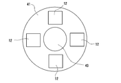
- FIG. 2 is an explanatory diagram showing a positional relationship between a plurality of excitation light units and reflection mirrors when the illumination device of FIG. 1 is viewed from the rear in the optical axis direction of a reflective fluorescent plate.
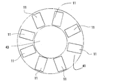
- FIG. 4 is an explanatory diagram showing a positional relationship between a plurality of excitation light units and reflection mirrors in a state in which the illumination device of FIG. 3 is viewed from the rear in the optical axis direction of a reflective fluorescent plate.
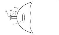
- FIG. drawing which shows the principal part in further another embodiment of the illuminating device of this invention.
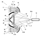
- FIG. 1 is an explanatory view showing an embodiment of the illumination device of the present invention.
- FIG. 2 is an explanatory diagram showing the positional relationship between a plurality of excitation light units and reflection mirrors when the illumination device of FIG. 1 is viewed from the rear of the reflective fluorescent plate in the optical axis direction.
- the arrangement positions of the plurality of excitation light units 11 are indicated by the arrangement positions of the radiation fins 12 provided on the back surface of each excitation light unit 11.
- the illumination device 10 includes a fluorescent light emitting member 20 having a reflective fluorescent plate 21 and an excitation light irradiation mechanism that irradiates the fluorescent plate 21 with excitation light.
- the illuminating device 10 radiates
- the “reflection type fluorescent plate” is a fluorescent plate in which the excitation light receiving surface and the fluorescent light emitting surface are formed on the same surface. Further, “emitted light from the reflective fluorescent plate” includes excitation light as well as fluorescence.
- the fluorescent light emitting member 20 is a member in which a substantially flat fluorescent plate 21 is provided on the surface of a flat substrate 22.
- the surface (right surface in FIG. 1) of the fluorescent plate 21 is an excitation light receiving surface and a fluorescent light emitting surface.
- the fluorescent plate 21 is made of a substantially flat fluorescent member, and a periodic structure (not shown) in which a plurality of convex portions are periodically arranged on the surface of the fluorescent member, that is, the surface of the fluorescent plate 21. Is formed.
- This periodic structure is, for example, two-dimensionally arranged in a state where convex portions having a substantially cone shape (specifically, a cone shape or a frustum shape) are densely packed.
- a light reflecting film made of silver or the like is provided on the back surface (left surface in FIG. 1) of the fluorescent plate 21.
- a bonding member (not shown) is interposed between the light reflection film and the substrate 22, and the fluorescent plate 21 is bonded onto the substrate 22 by the bonding member.
- the joining member solder, a silver sintered material, or the like is used from the viewpoint of exhaust heat. Further, a heat radiating member (not shown) made of a metal such as copper is disposed on the back surface of the substrate 22.
- the fluorescent plate 21 is a surface (excitation light receiving surface and fluorescent emitting surface). Specifically, the shape of the surface of the fluorescent plate 21 is preferably a circular shape rather than a square shape.
- the fluorescent member constituting the fluorescent plate 21 contains a fluorescent material, and is preferably made of a polycrystalline fluorescent material.
- the fluorescent member is made of a phosphor or a sintered body of a mixture of a phosphor and a ceramic binder. That is, the fluorescent member is composed of a fluorescent material.
- a sintered body of a mixture of a phosphor and a ceramic binder used as a fluorescent member nano-sized alumina particles are used as the ceramic binder. This sintered body is obtained by mixing several mass% to several tens mass% ceramic binder with respect to 100 mass% of the phosphor, pressing the mixture, and then firing.
- the polycrystalline phosphor constituting the fluorescent member can be obtained, for example, as follows. First, raw materials such as a base material, an activator, and a firing aid are pulverized by a ball mill or the like to obtain raw material fine particles of submicron or less. Next, the raw material fine particles are formed by, for example, a slip casting method and sintered. Thereafter, a polycrystalline phosphor having a porosity of 0.5% or less, for example, is obtained by subjecting the obtained sintered body to hot isostatic pressing.
- the phosphor constituting the fluorescent member include YAG: Ce, YAG: Pr, YAG: Sm, and LuAG: Ce.
- the activator doping amount is about 0.5 mol%.
- the thickness of the fluorescent member is preferably 0.05 to 2.0 mm from the viewpoint of fluorescence conversion efficiency and exhaust heat.
- the substrate 22 has a heat exhaust property, and is made of a material such as copper, an alloy of molybdenum and copper (Mo—Cu), an alloy of tungsten and copper (W—Cu), or the like. Moreover, it is preferable that the surface where the fluorescent plate 21 is arrange
- the thickness of the substrate 22 is, for example, 0.5 to 1.0 mm.
- the condensing optical system has two condensing members, a condensing lens 31 and a condensing mirror 35, and condenses the light emitted from the fluorescent plate 21 and guides it to the outside. Since the condensing optical system is constituted by two condensing members, the light emitted from the fluorescent plate 21 toward the condensing mirror 35 (specifically, toward the reflecting surface of the condensing mirror 35). Light) is captured and collected by the condenser mirror 35. Further, light emitted from the fluorescent plate 21 toward the condensing lens 31 is captured and collected by the condensing lens 31.
- the illuminating device 10 can be utilized with high efficiency.
- the condensing optical system being comprised by two condensing members, the size of the light radiated
- the light path of the light reflected by the reflecting surface of the condensing mirror 35 out of the light emitted from the fluorescent plate 21 is indicated by a broken line L3.
- the condensing lens 31 is a convex lens for condensing the emitted light from the fluorescent plate 21, and is separated from the fluorescent plate 21 at a position in front of the fluorescent plate 21 in the optical axis direction (right side in FIG. 1). Are arranged opposite each other.
- the condensing lens 31 is a disc-like convex lens having an outer diameter larger than the dimension of the fluorescent plate 21, and its optical axis coincides with the optical axis C of the fluorescent plate 21.
- the dimension (outer diameter) and the separation distance from the fluorescent plate 21 are based on the size of the lighting device 10 itself, the size of the fluorescent plate 21, the type and size of the condensing mirror 35, and the like. It is determined as appropriate in consideration of the relationship.
- the condensing mirror 35 is formed of an annular concave mirror having a light emission opening 37 formed at the front end, and a reflection surface for reflecting the emitted light from the fluorescent plate 21 is formed on the inner surface of the condensing mirror 35. ing.
- the condensing mirror 35 reflects and collects the light emitted from the fluorescent plate 21 in the direction other than the direction toward the light radiation opening 37 along the optical axis C of the fluorescent plate 21.
- the fluorescent plate 21 is disposed so as to surround it. That is, the light emission opening 37 is located in front of the fluorescent plate 21 in the optical axis direction, and the fluorescent plate 21 is located at the rear end side (left end side in FIG. 1) in the condensing space of the condensing mirror 35. Is arranged.
- the annular concave mirror constituting the condensing mirror 35 include a spheroidal mirror and a rotating parabolic mirror.
- the spheroid mirror has a spheroid reflecting surface centered on its optical axis, while the slewing paraboloid mirror is a rotating paraboloid centered on its optical axis. Having a reflective surface.
- the condensing mirror 35 is a spheroid mirror having a circular light emission aperture 37, and its optical axis coincides with the optical axis C of the fluorescent plate 21 and the optical axis of the condensing lens 31. Is arranged.
- the condensing point of the condensing mirror 35 that is, the second focal point coincides with the condensing point of the condensing lens 31, and the condensing point of the condensing optical system is configured by this condensing point.
- a circular through hole 38 is formed at the rear end (left end in FIG. 1) of the condensing mirror 35, and the fluorescent plate 21 is disposed at the center position of the through hole 38.
- the fluorescent plate 21 is located on the first focal point of the condenser mirror 35.
- a condensing lens 31 is disposed in the condensing space of the condensing mirror 35 at a position close to the light radiation opening 37.
- the opening diameter of the light radiation opening 37 is larger than the outer diameter of the condensing lens 31. That is, the outer diameter of the condensing lens 31 is smaller than the opening diameter of the light emission opening 37. Since the opening diameter of the light emission opening 37 is larger than the outer diameter of the condensing lens 31, the emitted light from the fluorescent plate 21 is captured by each of the condensing mirror 35 and the condensing lens 31. Light can be collected efficiently. Specifically, only the light that goes directly to the light radiation opening 37 without passing through the condensing mirror 35 out of the light emitted from the fluorescent plate 21 can be captured by the condensing lens 31.
- the reflected light from the reflecting surface of the condensing mirror 35 can be prevented from entering the condensing lens 31.
- the opening diameter of the light emitting opening 37 is larger than the outer diameter of the condensing lens 31, as shown in FIG. It can arrange
- the degree of freedom in designing the illumination device 10 can be increased, and further downsizing of the illumination device 10 can be achieved.
- the condensing lens 31 condenses only the light that goes to the direction other than the direction that goes to the reflecting surface of the condensing mirror 35 out of the light emitted from the fluorescent plate 21.
- the condensing lens 31 and the condensing mirror 35 are separated from each other at least in part, and between the outer peripheral edge of the condensing lens 31 and the inner surface (reflection surface) of the condensing mirror 35.
- the space 15 is formed by the space formed in the space.
- the gap 15 is positioned on the optical path from the excitation light from the excitation light irradiation mechanism to the fluorescent plate 21. That is, the excitation light receiving surface of the fluorescent plate 21 is irradiated with excitation light from the excitation light irradiation mechanism via the gap 15.
- the gap 15 preferably has an annular shape extending along the opening edge 37 ⁇ / b> A of the light emission opening 37 and the outer peripheral edge of the condensing lens 31 in the condensing mirror 35.
- This annular shape may be a continuous annular shape or an intermittent annular shape. Since the gap 15 has an annular shape, excitation light can be incident on the fluorescent plate 21 continuously or intermittently along the outer edge of the aperture edge 37A and the condensing lens 31. Uniformity of illuminance is obtained on the excitation light receiving surface of the plate 21. Therefore, since excitation light is not locally irradiated to a part of the excitation light receiving surface, the excitation light power of the excitation light can be increased.
- the condensing mirror 35 and the condensing lens 31 are spaced apart from the outer peripheral edge of the condensing lens 31 and the entire circumference of the inner surface of the condensing mirror 35. And between the outer periphery of the condensing lens 31 and the inner surface of the condensing mirror 35, the annular space
- the excitation light irradiation mechanism includes an excitation light source, and this excitation light source is constituted by a plurality (four in FIGS. 1 and 2) of excitation light units 11.
- the excitation light irradiation mechanism is preferably provided with an annular reflecting mirror 41 as shown in FIG. Since the reflection mirror 41 is provided, the excitation density of the excitation light can be lowered by the reflection mirror 41. Therefore, since the occurrence of luminance saturation in the fluorescent plate 21 can be suppressed, high fluorescence conversion efficiency can be obtained in the fluorescent plate 21. Further, since the reflection mirror 41 is provided, the degree of freedom of the arrangement position of the excitation light source (plurality of excitation light units 11) is increased, and thus the degree of freedom of design of the illumination device 10 is increased.
- the excitation light source can be arranged in parallel in the vicinity of the condenser mirror 35. Therefore, in the illuminating device 10, since the dimension of the fluorescent plate 21 in the optical axis direction can be reduced, the illuminating device 10 can be made small. Moreover, since the excitation light source and the fluorescent plate 21 can be cooled by a common cooling mechanism, the lighting device 10 can be further reduced in size.
- the plurality of excitation light units 11 are arranged in the vicinity of the rear end portion of the collector mirror 35 so as to surround the fluorescent plate 21 via the collector mirror 35. Further, each of the plurality of excitation light units 11 has an excitation light emission surface 11A located substantially on the same plane or parallel to the excitation light receiving surface of the fluorescent plate 21, and the excitation light reaching the reflection mirror 41. It arrange
- the plurality of excitation light units 11 are arranged at equal intervals along the circumferential direction of the outer surface of the condensing mirror 35.
- each of the plurality of excitation light units 11 is arranged so that the optical axis thereof is parallel to the optical axis C of the fluorescent plate 21. Moreover, in FIG. 1, the optical path of the light emitted from the excitation light unit 11 and reflected by the reflection mirror 41 is indicated by a solid line L1.
- any excitation light source may be used as long as it can emit the excitation light of the fluorescent plate 21. Accordingly, an excitation light source that emits light of an appropriate wavelength according to the type of phosphor constituting the fluorescent plate 21 is used. . Specifically, for example, those that emit light having a wavelength of 405 to 465 nm are used. Further, as the excitation light unit 11, for example, a laser light source such as a semiconductor laser is used. However, the form may include one laser light source or a plurality of laser light sources. A condensing lens may be arranged in front of a plurality of laser light sources in the optical axis direction (see FIG. 3).
- the excitation light is not limited to the light from the laser light source, but may be the light from the LED and the light from the lamp in which mercury, xenon or the like is enclosed.
- the wavelength of the excitation light is a main emission wavelength region emitted from the lamp or the like.
- the present invention is not limited to this.
- each of the plurality of pumping light units 11 is composed of a laser diode bank (LD bank).
- the radiation fin 12 is provided in the back surface (left surface in FIG. 1) of the some excitation light unit 11, respectively.
- the reflection mirror 41 is disposed so as to face the excitation light source and the fluorescent plate 21 at the front position (right position in FIG. 1) in the optical axis direction of the excitation light source (the plurality of excitation light units 11) and the condensing mirror 35. Yes.
- a reflection surface that reflects excitation light is formed on the surface of the reflection mirror 41 that faces the excitation light source and the fluorescent plate 21.
- the reflection mirror 41 has an annular shape extending along the opening edge 37 ⁇ / b> A of the condensing mirror 35.
- the reflecting mirror 41 may have a continuous annular shape or an intermittent annular shape. Specifically, the reflection mirror 41 may be a single one as shown in FIG. 1, or a plurality of reflection mirror elements arranged in an annular shape without gaps or at intervals.
- the reflection mirror 41 has a circular light emission opening 42 formed at the front end (left end in FIG. 1) and a circular through hole 43 formed at the rear end (right end in FIG. 1). It consists of a rotating parabolic mirror.
- the through-hole 43 has an inner diameter that is larger than the outer diameter of the condensing lens 31.
- the reflection mirror 41 is arranged so that its optical axis coincides with the optical axis C of the fluorescent plate 21.
- a fluorescence reflection optical member 45 that transmits excitation light and reflects fluorescence emitted from the fluorescence plate 21 in a direction toward the fluorescence plate 21.
- the fluorescent reflection optical member 45 is disposed on an optical path (hereinafter also referred to as “excitation light path”) from which excitation light from the excitation light source reaches the fluorescent plate 21.
- the fluorescence reflected by the fluorescent reflection optical member 45 and reaching the surface of the fluorescent plate 21 is reflected on the surface, or incident on the fluorescent plate 21 and reflected by the light reflecting film on the back surface.
- the light is emitted from the surface of the fluorescent plate 21 again.
- the fluorescent reflection optical member 45 is disposed to face the surface of the fluorescent plate 21.
- Preferable specific examples of the arrangement position of the fluorescent reflection optical member 45 include the following areas (1) and (2).
- region in the condensing space a region between the fluorescent plate 21 and the condensing lens 31 in the excitation light path.
- region in the condensing space an area between the light emitting aperture 37 of the condensing mirror 35 and the reflecting mirror 41 in the excitation light path.
- the fluorescent reflecting optical member 45 has an annular shape extending along the outer peripheral edge of the condensing lens 31 and the opening edge 37A in the condensing mirror 35 as shown in FIG. It is preferable that it has a shape.
- This annular shape may be a continuous annular shape or an intermittent annular shape.
- the optical member 45 for fluorescence reflection may be a single one as shown in FIG. 1, or a plurality of elements are arranged in a ring shape without gaps or at intervals. It may be a thing.
- the annular shape of the fluorescent member for fluorescent reflection 45 is fluorescence from the fluorescent plate 21 toward the condensing optical system (specifically, fluorescence toward the condensing lens 31 and fluorescence toward the reflecting surface of the condensing mirror 35). , And the fluorescent light emitted from the condensing optical system (specifically, the fluorescent light emitted from the condensing lens 31 and the fluorescent light emitted from the condensing mirror 35). It is preferable.
- the outer peripheral edge 45A of the fluorescent reflection optical member 45 is excited as shown in FIG. It is preferable that it is located inside the virtual cone surface S2 including the optical axis point on the light receiving surface and the opening edge 37A and extending along the optical axis C of the fluorescent plate 21. Further, as shown in FIG. 1, the inner peripheral edge 45 ⁇ / b> B includes an optical axis point on the excitation light receiving surface and an outer peripheral edge of the condensing lens 31, and extends virtually along the optical axis C of the fluorescent plate 21. It is preferable to be located outside the conical surface S1.
- the optical system includes the condensing point of the optical system and the opening edge 37 ⁇ / b> A, and is located outside the virtual conical surface extending along the optical axis C of the fluorescent plate 21.
- the optical axis point on the excitation light receiving surface is the intersection of the excitation light receiving surface of the fluorescent plate 21, that is, the surface of the fluorescent plate 21, and the optical axis C of the fluorescent plate 21.
- a wavelength selective mirror or the like can be used as the fluorescent reflection optical member 45.
- a circular light emission opening 46 is formed at the front end (left end in FIG. 1), and a circular through hole 47 is formed at the rear end (right end in FIG. 1). It consists of the formed wavelength selective concave mirror.
- a reflection surface that transmits excitation light and reflects fluorescence is formed on the inner surface thereof.
- the wavelength-selective concave mirror is arranged so that its optical axis coincides with the optical axis C of the fluorescent plate 21.
- the light-diffusion member 48 which has fluorescence scattering ability may be provided. preferable.
- This light diffusing member 48 is forward (in the optical axis direction) of the fluorescent reflection optical member 45 so that the reflected light from the fluorescent reflection optical member 45 is incident between the fluorescent plate 21 and the condensing lens 31.
- the light diffusing member 48 is fluorescent. It is disposed between the reflecting optical member 45 and the fluorescent plate 21. In the example of this figure, the light diffusing member 48 is disposed in the vicinity of the fluorescent plate 21 between the fluorescent reflecting optical member 45 and the fluorescent plate 21.
- the light diffusing member 48 is arranged, even if the fluorescent plate 21 does not have sufficient fluorescence scattering ability with respect to the fluorescence incident from the surface due to its configuration, the optical member for fluorescent reflection The fluorescence reflected by 45 can be sufficiently scattered and its traveling direction can be changed. Therefore, the light reflected by the fluorescence reflecting optical member 45 can be captured by the condensing optical system with high efficiency. As a result, it is possible to further increase the output.
- the light diffusing member 48 preferably has a shape and dimensions (vertical and horizontal dimensions) that allow all of the reflected light from the fluorescent reflecting optical member 45 to be incident from the viewpoint of fluorescence utilization efficiency.
- shape of the light diffusing member 48 considering the efficiency of capturing fluorescence by the condensing lens 31, the condensing mirror 35, and the fluorescent reflection optical member 45, the shape of the surface related to the light incident / exit Is preferably circular rather than square.
- the light diffusing member 48 is not limited to a flat plate-like shape, and has a rod-like shape such as a rod lens, a rod lens having Mie scattering characteristics, and a light pipe having a light scattering surface. There may be.
- a light scattering plate is used as the light diffusing member 48, and this scattering plate has larger vertical and horizontal dimensions than the fluorescent plate 21.
- the excitation light emitted from the plurality of excitation light units 11 is reflected by the reflection mirror 41 and enters the condensing space of the condensing mirror 35 via the gap 15.
- the excitation light that has entered the condensing space passes through the fluorescence reflecting optical member 45 and the light diffusion member 48 and enters the excitation light receiving surface of the fluorescent plate 21 in the fluorescent light emitting member 20, that is, the surface of the fluorescent plate 21.
- the fluorescent substance which comprises a fluorescent member is excited, and fluorescence is emitted.
- This fluorescence is emitted from the fluorescence emission surface of the fluorescence plate 21, that is, the surface of the fluorescence plate 21 together with the excitation light that has entered the fluorescence plate 21 but has not been converted to fluorescence, and is condensed via the light diffusion member 48.
- the light is collected by the light beam, passes through the through-hole 43 of the reflection mirror 41, and is emitted to the outside of the illumination device 10.
- the excitation light from the excitation light irradiation mechanism is irradiated to the fluorescent plate 21 through the gap 15. Therefore, since the excitation light irradiation mechanism and the condensing optical system have a large degree of design freedom, the excitation light irradiation mechanism and the condensing optical system are configured with a small number of members, and the excitation light irradiation mechanism and the condensing optical system are configured. In the system, in particular, the dimension of the fluorescent plate 21 in the optical axis direction can be easily reduced. As a result, the lighting device 10 can be downsized.
- the light emitted from the fluorescent plate 21 and the fluorescence diffused by the light diffusing member 48 can be captured and condensed with high efficiency by the condensing optical system and guided to the outside.
- the excitation light propagates in space, a high utilization rate of the excitation light can be obtained and the excitation light power of the excitation light can be increased.
- the illuminating device 10 it is possible to reduce the size, obtain high excitation light utilization efficiency, increase the excitation light power of the excitation light, and further increase the emission light from the fluorescent plate 21. Since it can be used efficiently, high output can be achieved.
- the irradiation device 10 is a small-sized one in which the dimension M1 in the optical axis direction of the fluorescent plate 21 is 211 mm and the dimension M2 in the direction perpendicular to the optical axis C of the fluorescent plate 21 is 160 mm. Can do. And in the small irradiation apparatus 10, an excitation light output can be set to 100W.
- a fluorescent reflection optical member 45 is provided, and the fluorescent reflection optical member 45 has an outer peripheral edge 45A located inside the virtual conical surface S2 and an inner peripheral edge 47B of the virtual conical surface. It has an annular shape located outside S1. Therefore, since the fluorescence directed from the fluorescent plate 21 toward the gap 15 can be reflected toward the fluorescent plate 21, it is possible to suppress the generation of fluorescence that is not collected by the condensing optical system and cannot be used, Therefore, high fluorescence utilization efficiency can be obtained. Further, the fluorescence reflecting optical member 45 does not reflect the fluorescence directed from the fluorescence plate 21 to the condensing optical system and the fluorescence emitted from the condensing optical system. As a result, it is possible to further increase the output.
- the traveling direction of the fluorescence reflected from the fluorescent reflecting optical member 45 toward the fluorescent plate 21 can be changed. Therefore, the light reflected by the fluorescence reflecting optical member 45 can be captured by the condensing optical system with high efficiency, and thus higher fluorescence utilization efficiency can be obtained. As a result, it is possible to further increase the output, and it is possible to easily obtain light of a desired color in the emitted light from the lighting device 10.
- FIG. 3 is an explanatory view showing another embodiment of the illuminating device of the present invention
- FIG. 4 shows a plurality of excitations when the illuminating device of FIG. 3 is viewed from the rear in the optical axis direction of the reflective fluorescent plate.
- It is explanatory drawing which shows the positional relationship of an optical unit and a reflective mirror.
- the fluorescent reflection optical member 45 is disposed in a region (outside the condensing space) between the light emitting opening 37 of the condensing mirror 35 and the reflecting mirror 41 in the excitation light path. Except for the fact that the light uniformizing member 19 is arranged, it has basically the same configuration as that of the illumination device 10 of FIG.
- the fluorescent light emitting member 20 the condensing optical system (the condensing lens 31 and the condensing mirror 35), the excitation light irradiation mechanism (excitation light source and reflection mirror 41), the fluorescent reflection optical member 45, and the light diffusion.
- the member 48 has basically the same configuration as that of the lighting device 10 of FIG. Further, the light converging lens 31, the condensing mirror 35, the reflecting mirror 41, and the fluorescent reflecting optical member 45 have their optical axes that coincide with the optical axis of the fluorescent plate 21, as in the illumination device 10 of FIG. Are arranged as follows.
- the condensing point (second focal point) of the condensing mirror 35 coincides with the condensing point of the condensing lens 31, and the condensing point of the condensing optical system is constituted by these condensing points.
- the optical path of the light emitted from the excitation light unit 11 and reflected by the reflection mirror 41 is indicated by a solid line L1.
- the light path of the light collected from the fluorescent plate 21 by the condensing lens 31 and emitted from the condensing lens 31 is indicated by a broken line L2
- the optical path of the light reflected on the reflecting surface is indicated by a broken line L3.
- the condensing lens 31 is disposed on the light emission opening 37 of the condensing mirror 35.
- An annular gap 15 is formed between the outer peripheral edge of the condensing lens 31 and the opening edge 37 ⁇ / b> A of the condensing mirror 35 so as to surround the condensing lens 31.
- the pumping light source is composed of eight pumping light units 11, and each of these eight pumping light units 11 includes a plurality (three in the example of FIG. 3) of laser light sources 52, A condensing lens 53 is arranged in front of the plurality of laser light sources 52 in the optical axis direction (right side in FIG. 3).
- the plurality of excitation light units 11 are arranged at equal intervals along the circumferential direction of the outer surface of the condensing mirror 35, as in the illumination device 10 of FIG. 1, and each of the plurality of excitation light units 11 is The optical axis is arranged so as to be parallel to the optical axis of the fluorescent plate 21.
- the excitation light source (a plurality of excitation light units 11) and the fluorescent plate 21 are arranged on a rectangular flat plate-like cooling plate (not shown). That is, the illumination device 50 is provided with a cooling mechanism (not shown) including a rectangular flat plate-like cooling plate, and this cooling mechanism is common to the excitation light source (the plurality of excitation light units 11) and the fluorescent plate 21. belongs to.
- the light uniformizing member 19 is for uniformizing the light collected by the condensing optical system and passing through the through hole 47 of the fluorescent reflecting optical member 45 and the through hole 43 of the reflecting mirror 41. It is arranged behind 41 in the optical axis direction (right side in FIG. 3).
- an integrator rod is used when the condensing mirror 35 is a spheroid mirror, while when the condensing mirror 35 is a parabolic mirror, a lens array is used. Used. In the example of this figure, an integrator rod is used as the light uniformizing member 19.
- the light uniformizing member 19 has an optical axis of the fluorescent plate 21, an optical axis of the condensing lens 31, an optical axis of the condensing mirror 35, an optical axis of the reflecting mirror 41, and a fluorescent reflecting optical member.
- the light incident surface 19A is disposed so as to be positioned on the condensing point of the condensing optical system.
- the excitation light emitted from the plurality of excitation light units 11 is reflected by the reflection mirror 41, passes through the fluorescent reflection optical member 45, and then passes through the gap portion 15 to be a condensing mirror. It is incident on the 35 condensing space.
- the excitation light that has entered the condensing space passes through the light diffusing member 48 and enters the excitation light receiving surface of the fluorescent plate 21 in the fluorescent light emitting member 20, that is, the surface of the fluorescent plate 21.
- the fluorescent substance which comprises a fluorescent member is excited, and fluorescence is emitted.
- This fluorescence is emitted from the fluorescence emission surface of the fluorescence plate 21, that is, the surface of the fluorescence plate 21, and is collected by the light collection optical system via the light diffusion member 48, and the through holes 47 of the fluorescence reflection optical member 45 and The light passes through the through-hole 43 of the reflection mirror 41, is made uniform by the light uniformizing member 19, and then emitted to the outside of the illumination device 50.
- the illumination device 50 is configured to irradiate the fluorescent plate 21 with the excitation light from the excitation light irradiation mechanism via the gap portion 15, similarly to the illumination device 10 of FIG. 1. Therefore, according to the illuminating device 50, as in the illuminating device 10 of FIG. 1, it is possible to reduce the size, to obtain high fluorescence utilization efficiency and to increase the excitation light power of the excitation light, Furthermore, since the emitted light from the fluorescent plate 21 can be used with high efficiency, high output can be achieved.
- the illumination device 50 is provided with a fluorescent reflection optical member 45.
- the fluorescent reflection optical member 45 has an inner peripheral edge 45B including a condensing point of the condensing optical system and an opening edge 37A, and a fluorescent plate. It has an annular shape located outside the virtual conical surface extending along the optical axis 21. Therefore, since the fluorescence directed from the fluorescent plate 21 toward the gap 15 can be reflected toward the fluorescent plate 21, it is possible to suppress the generation of fluorescence that is not collected by the condensing optical system and cannot be used, Therefore, high fluorescence utilization efficiency can be obtained. Further, the fluorescence reflecting optical member 45 does not reflect the fluorescence emitted from the light emission opening 37. As a result, it is possible to further increase the output.
- the light diffusing member 48 is provided in the lighting device 50, the traveling direction of the fluorescence reflected from the fluorescent reflecting optical member 45 toward the fluorescent plate 21 can be changed. Therefore, the light reflected by the fluorescence reflecting optical member 45 can be captured by the condensing optical system with high efficiency, and thus higher fluorescence utilization efficiency can be obtained. As a result, it is possible to further increase the output, and it is possible to easily obtain light of a desired color in the emitted light from the lighting device 50.
- a rod lens 61 that transmits excitation light and fluorescence emitted from the fluorescent plate 21 is disposed in front of the fluorescent plate 21 in the optical axis direction.
- the configuration may be such that the light emitted from the light enters the condensing space of the condensing mirror 35 via the rod lens 61.
- the excitation light from the excitation light source is incident on the excitation light receiving surface of the fluorescent plate 21 via the rod lens 61. It is possible to make the light uniform.
- the illuminating device of FIG. 5 has the same configuration as the illuminating device 10 of FIG. 1 except that the rod lens 61 is provided.
- the fluorescent plate is formed with a periodic structure layer that transmits excitation light and fluorescence emitted from the phosphor constituting the fluorescent member on the surface of the flat fluorescent member, and has a periodic structure formed on the surface. It may be what was done.
- the fluorescent plate may have a flat excitation light receiving surface.
- the fluorescent member constituting the fluorescent plate may contain excitation light and a minute scatterer that scatters fluorescence emitted from the fluorescent member constituting the fluorescent member.
- a lighting device (hereinafter also referred to as “lighting device (1)”) was manufactured according to the configuration of FIG.
- an excitation light unit (11) having a collimated excitation light size of 1.2 mm ⁇ 4 mm is used as an excitation light source, and YAG and Al 2 are used as a fluorescent plate (21). It was made of a sintered body of a mixture with O 3, and a light reflecting film was provided on the back surface, so that the back surface was equipped with a fluorescent member having a reflecting function.
- the condensing mirror (35) was a spheroid mirror having a first focal length of 16.7 mm and a second focal length of 190 mm.
- the reflection mirror (41) a parabolic mirror having a focal length of 160 mm and an outer diameter of 160 mm was used.
- a wavelength selective concave mirror was used as the fluorescent reflection optical member (45), and a light scattering plate was used as the light diffusion member (48).
- the dimension (M1) in the optical axis direction of the fluorescent plate (21) was 211 mm
- the dimension (M2) in the direction perpendicular to the optical axis of the fluorescent plate (21) was 160 mm. .
- the illuminating device (hereinafter referred to as “illumination”) having the same configuration as that of the illuminating device (1) except that the fluorescent reflection optical member (45) and the light diffusion member (48) are not provided.
- Device (2) was produced.
- the dimension (M1) in the optical axis direction of the fluorescent plate (21) is 211 mm, and the direction is perpendicular to the optical axis of the fluorescent plate (21).
- the dimension (M2) was 160 mm.
- the excitation light source was turned on and the fluorescence utilization efficiency was confirmed.
- the illumination device (1) had a fluorescence utilization efficiency of 63.6%
- the illumination device (2 ) Fluorescence utilization efficiency was 52.4%.
- Example 2 In the illuminating device (1) of Experimental Example 1, the illuminating device except that the fluorescent reflection optical member (45) is disposed at a position close to the excitation light source between the excitation light source and the reflection mirror (41).
- An illumination device having the same configuration as (1) hereinafter also referred to as “illumination device (3)” was manufactured.
- the fluorescence reflecting optical member (45) is arranged so as to reflect the fluorescence toward the reflecting mirror (41).
- the dimension (M1) in the optical axis direction of the fluorescent plate (21) is 211 mm, and the direction is perpendicular to the optical axis of the fluorescent plate (21).
- the dimension (M2) was 160 mm.
- an illumination device (hereinafter referred to as “illumination”) having the same configuration as that of the illumination device (3) except that the fluorescent reflection optical member (45) and the light diffusion member (48) are not provided.
- Device (4) was also produced.
- the dimension (M1) in the optical axis direction of the fluorescent plate (21) is 211 mm, and the direction perpendicular to the optical axis of the fluorescent plate (21).
- the dimension (M2) was 160 mm.
- the excitation light source was turned on and the fluorescence utilization efficiency was confirmed.
- the illumination device (3) had a fluorescence utilization efficiency of 54.7%, and the illumination device (4 ) Fluorescence utilization efficiency was 52.4%.
Landscapes
- Engineering & Computer Science (AREA)
- General Engineering & Computer Science (AREA)
- Non-Portable Lighting Devices Or Systems Thereof (AREA)
- Projection Apparatus (AREA)
- Microscoopes, Condenser (AREA)
- Investigating, Analyzing Materials By Fluorescence Or Luminescence (AREA)
Abstract
本発明は、高出力化および小型化を図ることのできる照明装置を提供することを目的とする。 本発明の照明装置は、反射型の蛍光プレートと、当該蛍光プレートの光軸方向前方に配置された集光性レンズと、当該集光性レンズの外径よりも大径の光放射開口を有し、当該光放射開口が当該蛍光プレートの光軸方向前方に位置するよう配置され、当該蛍光プレートからの出射光のうちの当該集光性レンズに向かう方向以外の方向に向かう光を反射して集光する環状の集光ミラーとを備え、励起光源からの励起光が、前記集光ミラーと前記集光性レンズとの間の空隙部を介して前記蛍光プレートに照射されることを特徴とする。
Description
本発明は、照明装置に関し、更に詳しくは、励起光によって蛍光を放射する蛍光プレートを備え、探照灯などに用いられる照明装置に関する。
従来、照明装置としては、レーザ光を励起光として蛍光プレートに照射し、当該蛍光プレートから蛍光を出射させ、その蛍光プレートからの蛍光を反射鏡などの光学系を介して外部に放射する構成のものが知られている(例えば、特許文献1参照。)。
具体的に、特許文献1においては、図6に示すように、複数の半導体レーザ素子71からの励起光の各々を光ファイバ73によって導光して反射型の蛍光プレート72に照射し、当該蛍光プレート72において蛍光に変換された光を放射する照明装置が開示されている。この照明装置においては、複数の光ファイバ73の光出射側部分が束ねられてバンドル部74が形成されており、そのバンドル部74には、当該複数の光ファイバ73のファイバ端よりなる光出射端が形成されている。また、照明装置には、蛍光プレート72の励起光受光面を取り囲むように凹面反射鏡75が配置されている。そして、凹面反射鏡75には貫通穴76が形成されており、この貫通穴76を介して、バンドル部74における光出射端から出射された励起光が蛍光プレート72に照射される。
図6において、77および78はレンズであり、79は反射ミラーであり、22は蛍光プレート72が配設された基板である。
具体的に、特許文献1においては、図6に示すように、複数の半導体レーザ素子71からの励起光の各々を光ファイバ73によって導光して反射型の蛍光プレート72に照射し、当該蛍光プレート72において蛍光に変換された光を放射する照明装置が開示されている。この照明装置においては、複数の光ファイバ73の光出射側部分が束ねられてバンドル部74が形成されており、そのバンドル部74には、当該複数の光ファイバ73のファイバ端よりなる光出射端が形成されている。また、照明装置には、蛍光プレート72の励起光受光面を取り囲むように凹面反射鏡75が配置されている。そして、凹面反射鏡75には貫通穴76が形成されており、この貫通穴76を介して、バンドル部74における光出射端から出射された励起光が蛍光プレート72に照射される。
図6において、77および78はレンズであり、79は反射ミラーであり、22は蛍光プレート72が配設された基板である。
このような構成の照明装置においては、蛍光プレート72からの出射光を外部に導光するための光学系、すなわち凹面反射鏡75に、励起光を通過させるための励起光通過路、具体的には貫通穴76が形成されているため、当該光学系のロスが大きい。そのため、十分な蛍光利用効率が得られない、という問題がある。しかも、複数の光ファイバ73が束ねられて形成されたバンドル部74を有するものであることから、当該バンドル部74の焼損の問題から高出力化には限界があり、近年における照明装置の高出力化の要請に応じることができない、という問題もある。
また、この照明装置においては、複数の半導体レーザ素子71からの励起光を、複数の光ファイバ73を用いて導光していることから、極めて多数の部材が必要とされるため、小型化を図ることができない、という問題がある。
また、この照明装置においては、複数の半導体レーザ素子71からの励起光を、複数の光ファイバ73を用いて導光していることから、極めて多数の部材が必要とされるため、小型化を図ることができない、という問題がある。
本発明は、以上のような事情に基づいてなされたものであって、その目的は、高出力化および小型化を図ることのできる照明装置を提供することにある。
本発明の照明装置は、反射型の蛍光プレートと、当該蛍光プレートの光軸方向前方に配置された集光性レンズと、当該集光性レンズの外径よりも大径の光放射開口を有し、当該光放射開口が当該蛍光プレートの光軸方向前方に位置するよう配置され、当該蛍光プレートからの出射光のうちの当該集光性レンズに向かう方向以外の方向に向かう光を反射して集光する環状の集光ミラーとを備え、
励起光源からの励起光が、前記集光ミラーと前記集光性レンズとの間の空隙部を介して前記蛍光プレートに照射されることを特徴とする。
励起光源からの励起光が、前記集光ミラーと前記集光性レンズとの間の空隙部を介して前記蛍光プレートに照射されることを特徴とする。
本発明の照明装置においては、前記励起光源からの励起光が前記蛍光プレートに至るまでの光路上に、前記励起光を透過し、前記蛍光プレートから出射される蛍光を、当該蛍光プレートに向かう方向に反射する蛍光反射用光学部材が配置されていることが好ましい。
本発明の照明装置においては、前記蛍光反射用光学部材は、前記光路における、前記蛍光プレートと前記集光性レンズとの間の領域に配置されていることが好ましい。
このような構成の本発明の照明装置においては、前記蛍光反射用光学部材は、前記集光性レンズの外周縁に沿って伸びる環状形状を有しており、
前記蛍光反射用光学部材は、当該蛍光反射用光学部材の外周縁が、前記蛍光プレートの励起光受光面における光軸点と前記集光ミラーにおける光放射開口の開口縁を含み、当該蛍光プレートの光軸に沿って伸びる仮想錐面の内側に位置し、当該蛍光反射用光学部材の内周縁が、当該光軸点と前記集光性レンズの外周縁とを含み、当該蛍光プレートの光軸に沿って伸びる仮想錐面の外側に位置するように配設されていることが好ましい。
このような構成の本発明の照明装置においては、前記蛍光反射用光学部材は、前記集光性レンズの外周縁に沿って伸びる環状形状を有しており、
前記蛍光反射用光学部材は、当該蛍光反射用光学部材の外周縁が、前記蛍光プレートの励起光受光面における光軸点と前記集光ミラーにおける光放射開口の開口縁を含み、当該蛍光プレートの光軸に沿って伸びる仮想錐面の内側に位置し、当該蛍光反射用光学部材の内周縁が、当該光軸点と前記集光性レンズの外周縁とを含み、当該蛍光プレートの光軸に沿って伸びる仮想錐面の外側に位置するように配設されていることが好ましい。
また、本発明の照明装置においては、前記集光ミラーの光軸方向前方に、当該集光ミラーにおける光放射開口の開口縁に沿って伸びる環状の反射ミラーが設けられており、
前記蛍光反射用光学部材は、前記光路における、前記集光ミラーの光放射開口と前記反射ミラーとの間の領域に配置されていることが好ましい。
このような構成の本発明の照明装置においては、前記蛍光反射用光学部材は、前記光放射開口の開口縁に沿って伸びる環状形状を有しており、
前記蛍光反射用光学部材は、当該蛍光反射用光学部材の内周縁が、前記集光ミラーおよび前記集光性レンズの集光点と前記光放射開口の開口縁を含み、前記蛍光プレートの光軸に沿って伸びる仮想錐面の外側に位置するように配設されていることが好ましい。
前記蛍光反射用光学部材は、前記光路における、前記集光ミラーの光放射開口と前記反射ミラーとの間の領域に配置されていることが好ましい。
このような構成の本発明の照明装置においては、前記蛍光反射用光学部材は、前記光放射開口の開口縁に沿って伸びる環状形状を有しており、
前記蛍光反射用光学部材は、当該蛍光反射用光学部材の内周縁が、前記集光ミラーおよび前記集光性レンズの集光点と前記光放射開口の開口縁を含み、前記蛍光プレートの光軸に沿って伸びる仮想錐面の外側に位置するように配設されていることが好ましい。
本発明の照明装置においては、前記蛍光プレートと前記集光性レンズとの間における、前記蛍光反射用光学部材の光軸方向前方に、蛍光拡散能を有する光拡散部材が配置されていることが好ましい。
本発明の照明装置においては、反射型の蛍光プレートからの出射光を集光するための集光部材として、集光性レンズと集光ミラーとが設けられており、これらの2つの集光部材の間の空隙部を介して、当該蛍光プレートに対して励起光が照射される。そのため、蛍光プレートに励起光を照射するための光学系および当該蛍光プレートからの出射光を集光して外部に導光するための光学系に大きな設計の自由度が得られることから、各光学系の小型化を容易に図ることができる。また、蛍光プレートからの出射光を高い効率で捕捉して集光し、外部に導光することができる。更に、2つの集光部材のいずれにも励起光を通過させるための励起光通過路を形成する必要がなく、よって励起光通過路が形成されていることに起因する光損失(蛍光損失)が生じることがない。また更に、励起光が空間伝搬されることから、高い励起光利用効率が得られる共に、励起光の励起光パワーを大きくすることができる。
従って、本発明の照明装置によれば、光学系を小さくすることによって小型化を図ることができ、また高い励起光利用効率が得られる共に励起光の励起光パワーを大きくすることができ、更に蛍光プレートからの出射光を高い効率で利用することができるため、高出力化を図ることができる。
従って、本発明の照明装置によれば、光学系を小さくすることによって小型化を図ることができ、また高い励起光利用効率が得られる共に励起光の励起光パワーを大きくすることができ、更に蛍光プレートからの出射光を高い効率で利用することができるため、高出力化を図ることができる。
また、本発明の照明装置においては、蛍光反射用光学部材を配設することにより、蛍光プレートから空隙部に向かう蛍光を、当該蛍光プレートに向かって反射することができる。そのため、集光部材によって集光されずに利用不可能となる蛍光の発生を抑制できることから、高い蛍光利用効率が得られる。その結果、より一層の高出力化を図ることができる。
このような構成の本発明の照明装置においては、更に光拡散部材を配設することにより、蛍光反射用光学部材から蛍光プレートに向かって反射された蛍光の進行方向を変更することができる。そのため、蛍光反射用光学部材によって反射された蛍光を、高い効率で集光性レンズまたは集光ミラーに捕捉させることができ、よってより高い蛍光利用効率が得られる。その結果、更なるより一層の高出力化を図ることができ、また照明装置からの放射光において、所望の色味の光を容易に得ることができる。
このような構成の本発明の照明装置においては、更に光拡散部材を配設することにより、蛍光反射用光学部材から蛍光プレートに向かって反射された蛍光の進行方向を変更することができる。そのため、蛍光反射用光学部材によって反射された蛍光を、高い効率で集光性レンズまたは集光ミラーに捕捉させることができ、よってより高い蛍光利用効率が得られる。その結果、更なるより一層の高出力化を図ることができ、また照明装置からの放射光において、所望の色味の光を容易に得ることができる。
以下、本発明の照明装置の実施の形態について説明する。
図1は、本発明の照明装置の一実施形態を示す説明図である。また、図2は、図1の照明装置を反射型の蛍光プレートの光軸方向後方から見た状態において、複数の励起光ユニットと反射ミラーとの位置関係を示す説明図である。この図2においては、複数の励起光ユニット11の配置位置が、各励起光ユニット11の裏面に設けられた放熱フィン12の配置位置によって示されている。
この照明装置10は、図1に示すように、反射型の蛍光プレート21を有する蛍光発光部材20と、蛍光プレート21に対して励起光を照射する励起光照射機構とを備えている。そして、照明装置10は、蛍光プレート21からの出射光を、環状の集光ミラー35と集光性レンズ31とよりなる集光光学系を介して外部に放射するものである。
ここに、本発明において、「反射型の蛍光プレート」とは、励起光受光面と蛍光出射面とが同一面上に形成された蛍光プレートである。また、「反射型の蛍光プレートからの出射光」は、蛍光と共に励起光を含むものである。
図1は、本発明の照明装置の一実施形態を示す説明図である。また、図2は、図1の照明装置を反射型の蛍光プレートの光軸方向後方から見た状態において、複数の励起光ユニットと反射ミラーとの位置関係を示す説明図である。この図2においては、複数の励起光ユニット11の配置位置が、各励起光ユニット11の裏面に設けられた放熱フィン12の配置位置によって示されている。
この照明装置10は、図1に示すように、反射型の蛍光プレート21を有する蛍光発光部材20と、蛍光プレート21に対して励起光を照射する励起光照射機構とを備えている。そして、照明装置10は、蛍光プレート21からの出射光を、環状の集光ミラー35と集光性レンズ31とよりなる集光光学系を介して外部に放射するものである。
ここに、本発明において、「反射型の蛍光プレート」とは、励起光受光面と蛍光出射面とが同一面上に形成された蛍光プレートである。また、「反射型の蛍光プレートからの出射光」は、蛍光と共に励起光を含むものである。
蛍光発光部材20は、平板状の基板22の表面に、略平板状の蛍光プレート21が設けられたものである。
この図の例において、蛍光プレート21においては、その表面(図1における右面)が励起光受光面とされていると共に蛍光出射面とされている。
この図の例において、蛍光プレート21においては、その表面(図1における右面)が励起光受光面とされていると共に蛍光出射面とされている。
蛍光プレート21は、略平板状の蛍光部材よりなるものであり、この蛍光部材の表面、すなわち蛍光プレート21の表面には、複数の凸部が周期的に配列されてなる周期構造(図示省略)が形成されている。この周期構造は、例えば略錐形状(具体的には、錐状または錐台状)の凸部が密集した状態で二次元周期的に配列されてなるものである。
また、蛍光プレート21の裏面(図1における左面)には、銀などよりなる光反射膜が設けられている。更に、光反射膜と基板22との間には、接合部材(図示省略)が介在されており、当該接合部材によって蛍光プレート21が基板22上に接合されている。接合部材としては、排熱性の観点から、半田および銀焼結材などが用いられる。また、基板22の裏面には、例えば銅などの金属よりなる放熱部材(図示省略)が配置されている。
ここに、蛍光プレート21は、集光性レンズ31、集光ミラー35および後述する蛍光反射用光学部材45による蛍光の捕捉の効率を考慮すると、励起光受光面および蛍光出射面とされる面(具体的には、蛍光プレート21の表面)の形状が正方形状であるよりも円形状であることが好ましい。
また、蛍光プレート21の裏面(図1における左面)には、銀などよりなる光反射膜が設けられている。更に、光反射膜と基板22との間には、接合部材(図示省略)が介在されており、当該接合部材によって蛍光プレート21が基板22上に接合されている。接合部材としては、排熱性の観点から、半田および銀焼結材などが用いられる。また、基板22の裏面には、例えば銅などの金属よりなる放熱部材(図示省略)が配置されている。
ここに、蛍光プレート21は、集光性レンズ31、集光ミラー35および後述する蛍光反射用光学部材45による蛍光の捕捉の効率を考慮すると、励起光受光面および蛍光出射面とされる面(具体的には、蛍光プレート21の表面)の形状が正方形状であるよりも円形状であることが好ましい。
蛍光プレート21を構成する蛍光部材は、蛍光体が含有されてなるものであり、好ましくは多結晶の蛍光体よりなるものである。具体的には、この蛍光部材は、蛍光体よりなるもの、または蛍光体とセラミックバインダーとの混合物の焼結体よりなるものである。すなわち、蛍光部材は、蛍光体によって構成されたものである。
ここに、蛍光部材として用いられる、蛍光体とセラミックバインダーとの混合物の焼結体においては、セラミックバインダーとしてナノサイズのアルミナ粒子が用いられる。そして、この焼結体は、蛍光体100質量%に対して数質量%~数十質量%のセラミックバインダーを混合し、その混合物をプレスした後、焼成することによって得られるものである。
ここに、蛍光部材として用いられる、蛍光体とセラミックバインダーとの混合物の焼結体においては、セラミックバインダーとしてナノサイズのアルミナ粒子が用いられる。そして、この焼結体は、蛍光体100質量%に対して数質量%~数十質量%のセラミックバインダーを混合し、その混合物をプレスした後、焼成することによって得られるものである。
蛍光部材を構成する多結晶の蛍光体は、例えば以下のようにして得ることができる。先ず、母材、賦活材および焼成助剤などの原材料をボールミルなどによって粉砕処理することによって、サブミクロン以下の原材料微粒子を得る。次いで、この原材料微粒子を例えばスリップキャスト法によって成形して、焼結する。その後、得られた焼結体に対して熱間等方圧加圧加工を施すことによって、気孔率が例えば0.5%以下の多結晶の蛍光体が得られる。
蛍光部材を構成する蛍光体の具体例としては、YAG:Ce、YAG:Pr、YAG:SmおよびLuAG:Ceなどが挙げられる。このような蛍光体において、賦活材のドープ量は、0.5mol%程度である。
また、蛍光部材の厚みは、蛍光変換効率および排熱性の観点から、0.05~2.0mmであることが好ましい。
基板22は、排熱性を有するものであり、銅、モリブデンと銅の合金(Mo-Cu)およびタングステンと銅の合金(W-Cu)などの材料よりなるものが用いられる。
また、基板22は、排熱性の観点から、蛍光プレート21が配設される表面が、当該蛍光プレート21の裏面よりも縦横寸法が大きくて、大きな面積を有するものであることが好ましい。
また、基板22の厚みは、例えば0.5~1.0mmである。
また、基板22は、排熱性の観点から、蛍光プレート21が配設される表面が、当該蛍光プレート21の裏面よりも縦横寸法が大きくて、大きな面積を有するものであることが好ましい。
また、基板22の厚みは、例えば0.5~1.0mmである。
集光光学系は、集光性レンズ31と集光ミラー35との2つの集光部材を有し、蛍光プレート21からの出射光を集光して外部に導光するものである。
集光光学系が2つの集光部材によって構成されていることにより、蛍光プレート21からの出射光のうちの集光ミラー35に向かう光(具体的には、集光ミラー35の反射面に向かう光)が当該集光ミラー35によって捕捉されて集光される。また、蛍光プレート21からの出射光のうちの集光性レンズ31に向かう光が当該集光性レンズ31によって捕捉されて集光される。そのため、蛍光プレート21からの出射光に含まれる蛍光が散乱光であっても、当該出射光を高い効率で捕捉して確実に集光することができる。その結果、照明装置10においては、蛍光プレート21からの出射光を高い効率で利用することができる。
また、集光光学系が2つの集光部材によって構成されていることによれば、照明装置10から放射される光のサイズを、他の集光部材を用いることなく極めて小さくすることができる。そのため、照明装置10からの放射光のサイズを容易に制御できることから、当該照明装置10を種々の用途に用いることができる。
図1においては、蛍光プレート21からの出射光のうちの集光ミラー35の反射面によって反射された光の光路が破線L3によって示されている。
集光光学系が2つの集光部材によって構成されていることにより、蛍光プレート21からの出射光のうちの集光ミラー35に向かう光(具体的には、集光ミラー35の反射面に向かう光)が当該集光ミラー35によって捕捉されて集光される。また、蛍光プレート21からの出射光のうちの集光性レンズ31に向かう光が当該集光性レンズ31によって捕捉されて集光される。そのため、蛍光プレート21からの出射光に含まれる蛍光が散乱光であっても、当該出射光を高い効率で捕捉して確実に集光することができる。その結果、照明装置10においては、蛍光プレート21からの出射光を高い効率で利用することができる。
また、集光光学系が2つの集光部材によって構成されていることによれば、照明装置10から放射される光のサイズを、他の集光部材を用いることなく極めて小さくすることができる。そのため、照明装置10からの放射光のサイズを容易に制御できることから、当該照明装置10を種々の用途に用いることができる。
図1においては、蛍光プレート21からの出射光のうちの集光ミラー35の反射面によって反射された光の光路が破線L3によって示されている。
集光性レンズ31は、蛍光プレート21からの出射光を集光するための凸レンズであり、蛍光プレート21の光軸方向前方(図1における右方)位置において、当該蛍光プレート21と離間した状態で対向配置されている。
図の例において、集光性レンズ31は、円盤状の凸レンズであって、蛍光プレート21の寸法よりも大きな外径を有するものであり、その光軸が蛍光プレート21の光軸Cと一致するように配置されている。
図の例において、集光性レンズ31は、円盤状の凸レンズであって、蛍光プレート21の寸法よりも大きな外径を有するものであり、その光軸が蛍光プレート21の光軸Cと一致するように配置されている。
集光性レンズ31において、寸法(外径)および蛍光プレート21との離間距離は、照明装置10自体の大きさなどに基づいて、蛍光プレート21の寸法や集光ミラー35の種類および寸法などとの関係を考慮して適宜に定められる。
集光ミラー35は、前端に光放射開口37が形成された環状凹面鏡よりなるものであり、当該集光ミラー35の内表面には、蛍光プレート21からの出射光を反射する反射面が形成されている。この集光ミラー35は、蛍光プレート21からの出射光のうちの光放射開口37に向かう方向以外の方向に向かう光を、当該蛍光プレート21の光軸Cに沿って反射して集光するよう、蛍光プレート21を取り囲むように配置されている。すなわち、光放射開口37が蛍光プレート21の光軸方向前方に位置しており、蛍光プレート21は、集光ミラー35の集光空間内における、後端側(図1における左端側)の位置に配置されている。
集光ミラー35を構成する環状凹面鏡の具体例としては、回転楕円面鏡および回転放物面鏡が挙げられる。なお、回転楕円面鏡とは、その光軸を中心とする回転楕円面状の反射面を有するものであり、一方、回転放物面鏡とは、その光軸を中心とする回転放物面状の反射面を有するものである。
図の例において、集光ミラー35は、光放射開口37が円形状の回転楕円面鏡であり、その光軸が蛍光プレート21の光軸Cおよび集光性レンズ31の光軸と一致するように配置されている。また、集光ミラー35の集光点、すなわち第2焦点は、集光性レンズ31の集光点と一致しており、この集光点によって集光光学系の集光点が構成されている。また、集光ミラー35の後端(図1における左端)には、円形状の貫通孔38が形成されており、この貫通孔38の中央位置に、蛍光プレート21が配置されている。そして、蛍光プレート21は、集光ミラー35の第1焦点上に位置している。更に、集光ミラー35の集光空間内には、光放射開口37に近接した位置に、集光性レンズ31が配置されている。
集光ミラー35を構成する環状凹面鏡の具体例としては、回転楕円面鏡および回転放物面鏡が挙げられる。なお、回転楕円面鏡とは、その光軸を中心とする回転楕円面状の反射面を有するものであり、一方、回転放物面鏡とは、その光軸を中心とする回転放物面状の反射面を有するものである。
図の例において、集光ミラー35は、光放射開口37が円形状の回転楕円面鏡であり、その光軸が蛍光プレート21の光軸Cおよび集光性レンズ31の光軸と一致するように配置されている。また、集光ミラー35の集光点、すなわち第2焦点は、集光性レンズ31の集光点と一致しており、この集光点によって集光光学系の集光点が構成されている。また、集光ミラー35の後端(図1における左端)には、円形状の貫通孔38が形成されており、この貫通孔38の中央位置に、蛍光プレート21が配置されている。そして、蛍光プレート21は、集光ミラー35の第1焦点上に位置している。更に、集光ミラー35の集光空間内には、光放射開口37に近接した位置に、集光性レンズ31が配置されている。
そして、集光光学系においては、光放射開口37の開口径が、集光性レンズ31の外径よりも大径とされている。すなわち、集光性レンズ31の外径は、光放射開口37の開口径よりも小径とされている。
光放射開口37の開口径が集光性レンズ31の外径よりも大径であることにより、蛍光プレート21からの出射光を、集光ミラー35および集光性レンズ31の各々によって捕捉して効率的に集光することができる。具体的には、蛍光プレート21からの出射光のうちの集光ミラー35を介することなく直接的に光放射開口37に向かう光のみを集光性レンズ31によって捕捉させることができる。すなわち、集光ミラー35の反射面からの反射光が集光性レンズ31に入射されないようにすることができる。また、光放射開口37の開口径が集光性レンズ31の外径よりも大径であることによれば、図1に示されているように、集光性レンズ31を、集光ミラー35の集光空間内に配置することができる。そのため、照明装置10において、蛍光プレート21の光軸方向(図1における左右方向)の寸法を小さくすることができることから、照明装置10を小型のものとすることができる。その上、励起光入射機構の構成を簡単なものとすることができることから、照明装置10の設計の自由度が大きくなると共に、照明装置10の更なる小型化を図ることができる。
この図の例において、集光性レンズ31は、蛍光プレート21からの出射光のうちの集光ミラー35の反射面に向かう方向以外の方向に向かう光のみを集光している。
光放射開口37の開口径が集光性レンズ31の外径よりも大径であることにより、蛍光プレート21からの出射光を、集光ミラー35および集光性レンズ31の各々によって捕捉して効率的に集光することができる。具体的には、蛍光プレート21からの出射光のうちの集光ミラー35を介することなく直接的に光放射開口37に向かう光のみを集光性レンズ31によって捕捉させることができる。すなわち、集光ミラー35の反射面からの反射光が集光性レンズ31に入射されないようにすることができる。また、光放射開口37の開口径が集光性レンズ31の外径よりも大径であることによれば、図1に示されているように、集光性レンズ31を、集光ミラー35の集光空間内に配置することができる。そのため、照明装置10において、蛍光プレート21の光軸方向(図1における左右方向)の寸法を小さくすることができることから、照明装置10を小型のものとすることができる。その上、励起光入射機構の構成を簡単なものとすることができることから、照明装置10の設計の自由度が大きくなると共に、照明装置10の更なる小型化を図ることができる。
この図の例において、集光性レンズ31は、蛍光プレート21からの出射光のうちの集光ミラー35の反射面に向かう方向以外の方向に向かう光のみを集光している。
また、集光性レンズ31と集光ミラー35とは少なくとも一部において離間した状態とされており、その集光性レンズ31の外周縁と集光ミラー35の内表面(反射面)との間に形成される空間よって空隙部15が構成されている。この空隙部15は、励起光照射機構からの励起光が蛍光プレート21に至るまでの光路上に位置される。すなわち、蛍光プレート21の励起光受光面には、空隙部15を介して励起光照射機構からの励起光が照射される。
この空隙部15は、集光ミラー35における光放射開口37の開口縁37Aおよび集光性レンズ31の外周縁に沿って伸びる環状形状を有することが好ましい。この環状形状は、連続的な環状形状であってもよく、また断続的な環状形状であってもよい。
空隙部15が環状形状であることにより、蛍光プレート21に対して、開口縁37Aおよび集光性レンズ31の外周縁に沿って連続的または断続的に励起光を入射させることができるため、蛍光プレート21の励起光受光面において照度の均一性が得られる。そのため、励起光受光面の一部に励起光が局所的に照射されることがないことから、励起光の励起光パワーを大きくすることができる。
この図の例において、集光ミラー35と集光性レンズ31とは、集光性レンズ31の外周縁および集光ミラー35の内表面の全周にわたって離間している。そして、集光性レンズ31の外周縁と集光ミラー35の内表面との間には、集光性レンズ31を包囲するよう、集光性レンズ31の外周縁に沿って伸びる円環状の空隙部15が形成されている。
この空隙部15は、集光ミラー35における光放射開口37の開口縁37Aおよび集光性レンズ31の外周縁に沿って伸びる環状形状を有することが好ましい。この環状形状は、連続的な環状形状であってもよく、また断続的な環状形状であってもよい。
空隙部15が環状形状であることにより、蛍光プレート21に対して、開口縁37Aおよび集光性レンズ31の外周縁に沿って連続的または断続的に励起光を入射させることができるため、蛍光プレート21の励起光受光面において照度の均一性が得られる。そのため、励起光受光面の一部に励起光が局所的に照射されることがないことから、励起光の励起光パワーを大きくすることができる。
この図の例において、集光ミラー35と集光性レンズ31とは、集光性レンズ31の外周縁および集光ミラー35の内表面の全周にわたって離間している。そして、集光性レンズ31の外周縁と集光ミラー35の内表面との間には、集光性レンズ31を包囲するよう、集光性レンズ31の外周縁に沿って伸びる円環状の空隙部15が形成されている。
励起光照射機構は、励起光源を備えており、この励起光源は、複数(図1および図2においては4つ)の励起光ユニット11によって構成されている。
そして、励起光照射機構には、図1に示されているように、環状の反射ミラー41が設けられていることが好ましい。
反射ミラー41が設けられていることにより、当該反射ミラー41によって励起光の励起密度を低くすることができる。そのため、蛍光プレート21における輝度飽和の発生を抑制することができることから、当該蛍光プレート21において高い蛍光変換効率を得ることができる。また、反射ミラー41が設けられていることによれば、励起光源(複数の励起光ユニット11)の配置位置の自由度が大きくなり、よって照明装置10の設計の自由度が大きくなる。故に、図1に示されているように、励起光源を、集光ミラー35の近傍位置に並列配置することができる。そのため、照明装置10において、蛍光プレート21の光軸方向の寸法を小さくすることができることから、当該照明装置10を小型のものとすることができる。また、励起光源と蛍光プレート21とを共通の冷却機構によって冷却することができるため、照明装置10の更なる小型化を図ることができる。
そして、励起光照射機構には、図1に示されているように、環状の反射ミラー41が設けられていることが好ましい。
反射ミラー41が設けられていることにより、当該反射ミラー41によって励起光の励起密度を低くすることができる。そのため、蛍光プレート21における輝度飽和の発生を抑制することができることから、当該蛍光プレート21において高い蛍光変換効率を得ることができる。また、反射ミラー41が設けられていることによれば、励起光源(複数の励起光ユニット11)の配置位置の自由度が大きくなり、よって照明装置10の設計の自由度が大きくなる。故に、図1に示されているように、励起光源を、集光ミラー35の近傍位置に並列配置することができる。そのため、照明装置10において、蛍光プレート21の光軸方向の寸法を小さくすることができることから、当該照明装置10を小型のものとすることができる。また、励起光源と蛍光プレート21とを共通の冷却機構によって冷却することができるため、照明装置10の更なる小型化を図ることができる。
複数の励起光ユニット11は、集光ミラー35の後端部分の近傍位置に、当該集光ミラー35を介して蛍光プレート21を取り囲むように配置されている。
また、複数の励起光ユニット11は、各々、その励起光出射面11Aが、蛍光プレート21の励起光受光面と略同一平面上あるいは平行に位置すると共に、反射ミラー41に至るまでの励起光の進行が集光ミラー35によって阻害されることのないように配置される。
この図の例において、複数の励起光ユニット11は、集光ミラー35の外表面の周方向に沿って等間隔で配置されている。また、複数の励起光ユニット11の各々は、その光軸が、蛍光プレート21の光軸Cと平行となるように配置されている。
また、図1においては、励起光ユニット11から出射され、反射ミラー41によって反射された光の光路が実線L1によって示されている。
また、複数の励起光ユニット11は、各々、その励起光出射面11Aが、蛍光プレート21の励起光受光面と略同一平面上あるいは平行に位置すると共に、反射ミラー41に至るまでの励起光の進行が集光ミラー35によって阻害されることのないように配置される。
この図の例において、複数の励起光ユニット11は、集光ミラー35の外表面の周方向に沿って等間隔で配置されている。また、複数の励起光ユニット11の各々は、その光軸が、蛍光プレート21の光軸Cと平行となるように配置されている。
また、図1においては、励起光ユニット11から出射され、反射ミラー41によって反射された光の光路が実線L1によって示されている。
励起光源としては、蛍光プレート21の励起光を放射することのできるものであればよく、よって蛍光プレート21を構成する蛍光体の種類などに応じて適宜の波長の光を放射するものが用いられる。具体的には、例えば波長405~465nmの光を放射するものが用いられる。
また、励起光ユニット11としては、例えば半導体レーザ等のレーザ光源などが用いられるが、その形態は、1つのレーザ光源を備えたものであってもよく、あるいは複数のレーザ光源を備え、これらの複数のレーザ光源の光軸方向前方に集光性レンズが配置されてなるものであってもよい(図3参照)。
ここに、励起光は、レーザ光源からの光に限定されるものではなく、LEDの光、および水銀、キセノン等が封入されたランプからの光であってもよい。なお、ランプやLEDのように放射波長に幅を持つ光源を利用した場合、励起光の波長はランプ等から放射される主たる放射波長の領域である。ただし、本発明においては、これに限定されるものではない。
図の例において、複数の励起光ユニット11は、各々、レーザダイオードバンク(LDバンク)よりなるものである。また、複数の励起光ユニット11の裏面(図1における左面)には、各々、放熱フィン12が設けられている。
また、励起光ユニット11としては、例えば半導体レーザ等のレーザ光源などが用いられるが、その形態は、1つのレーザ光源を備えたものであってもよく、あるいは複数のレーザ光源を備え、これらの複数のレーザ光源の光軸方向前方に集光性レンズが配置されてなるものであってもよい(図3参照)。
ここに、励起光は、レーザ光源からの光に限定されるものではなく、LEDの光、および水銀、キセノン等が封入されたランプからの光であってもよい。なお、ランプやLEDのように放射波長に幅を持つ光源を利用した場合、励起光の波長はランプ等から放射される主たる放射波長の領域である。ただし、本発明においては、これに限定されるものではない。
図の例において、複数の励起光ユニット11は、各々、レーザダイオードバンク(LDバンク)よりなるものである。また、複数の励起光ユニット11の裏面(図1における左面)には、各々、放熱フィン12が設けられている。
反射ミラー41は、励起光源(複数の励起光ユニット11)および集光ミラー35の光軸方向前方位置(図1における右方位置)において、励起光源および蛍光プレート21と対向するよう配設されている。この反射ミラー41における励起光源および蛍光プレート21と対向する表面には、励起光を反射する反射面が形成されている。そして、反射ミラー41は、集光ミラー35における開口縁37Aに沿って伸びる環状形状を有している。
この反射ミラー41の環状形状は、連続的な環状形状であってもよく、また断続的な環状形状であってよい。具体的には、反射ミラー41は、図1に示されているように単一のものであってもよく、あるいは複数の反射ミラー要素が、隙間なくまたは間隔をあけて環状に配列されたものであってもよい。
この図の例において、反射ミラー41は、前端(図1における左端)に、円形状の光放射開口42が形成され、後端(図1における右端)に、円形状の貫通孔43が形成された回転放物面鏡よりなるものである。この貫通孔43は、集光性レンズ31の外径よりも大径の内径を有している。また、反射ミラー41は、その光軸が蛍光プレート21の光軸Cと一致するように配置されている。
この反射ミラー41の環状形状は、連続的な環状形状であってもよく、また断続的な環状形状であってよい。具体的には、反射ミラー41は、図1に示されているように単一のものであってもよく、あるいは複数の反射ミラー要素が、隙間なくまたは間隔をあけて環状に配列されたものであってもよい。
この図の例において、反射ミラー41は、前端(図1における左端)に、円形状の光放射開口42が形成され、後端(図1における右端)に、円形状の貫通孔43が形成された回転放物面鏡よりなるものである。この貫通孔43は、集光性レンズ31の外径よりも大径の内径を有している。また、反射ミラー41は、その光軸が蛍光プレート21の光軸Cと一致するように配置されている。
また、照明装置10においては、図1に示されているように、励起光を透過して、蛍光プレート21から出射される蛍光を、蛍光プレート21に向かう方向に反射する蛍光反射用光学部材45が設けられていることが好ましい。この蛍光反射用光学部材45は、励起光源からの励起光が蛍光プレート21に至るまでの光路(以下、「励起光路」ともいう。)上に配置される。
蛍光反射用光学部材45が設けられていることにより、蛍光プレート21からの出射光のうちの空隙部15に向かう蛍光、すなわち集光光学系に向かう方向以外の方向に向かう蛍光を、当該蛍光プレート21に向かって反射することができる。そのため、集光光学系によって集光されずに利用不可能となる蛍光の発生を抑制することができる。
ここに、蛍光反射用光学部材45によって反射され、蛍光プレート21の表面に到達した蛍光は、その表面で反射される、あるいは蛍光プレート21に入射して裏面の光反射膜によって反射されることなどにより、再び蛍光プレート21の表面から出射される。
蛍光反射用光学部材45が設けられていることにより、蛍光プレート21からの出射光のうちの空隙部15に向かう蛍光、すなわち集光光学系に向かう方向以外の方向に向かう蛍光を、当該蛍光プレート21に向かって反射することができる。そのため、集光光学系によって集光されずに利用不可能となる蛍光の発生を抑制することができる。
ここに、蛍光反射用光学部材45によって反射され、蛍光プレート21の表面に到達した蛍光は、その表面で反射される、あるいは蛍光プレート21に入射して裏面の光反射膜によって反射されることなどにより、再び蛍光プレート21の表面から出射される。
蛍光反射用光学部材45は、蛍光プレート21の表面に対向配置されることが好ましい。
蛍光反射用光学部材45の配置位置の好ましい具体例としては、下記の(1)および(2)の領域が挙げられる。
蛍光反射用光学部材45の配置位置の好ましい具体例としては、下記の(1)および(2)の領域が挙げられる。
(1)図1に示されているように、励起光路における、蛍光プレート21と集光性レンズ31との間の領域(以下、「集光空間内領域」ともいう。)
(2)後述する図3に示されているように、励起光路における、集光ミラー35の光放射開口37と反射ミラー41との間の領域(以下、「集光空間外領域」ともいう。)
(2)後述する図3に示されているように、励起光路における、集光ミラー35の光放射開口37と反射ミラー41との間の領域(以下、「集光空間外領域」ともいう。)
また、蛍光反射用光学部材45は、蛍光集光性の観点から、図1に示されているように、集光性レンズ31の外周縁および集光ミラー35における開口縁37Aに沿って伸びる環状形状を有するものであることが好ましい。この環状形状は、連続的な環状形状であってもよく、また断続的な環状形状であってもよい。具体的には、蛍光反射用光学部材45は、図1に示されているように単一のものであってもよく、あるいは複数の要素が、隙間なくまたは間隔をあけて環状に配列されたものであってもよい。
そして、蛍光反射用蛍光部材45の環状形状は、蛍光プレート21から集光光学系に向かう蛍光(具体的には、集光性レンズ31に向かう蛍光および集光ミラー35の反射面に向かう蛍光)、および集光光学系から出射される蛍光(具体的には、集光性レンズ31から出射される蛍光および集光ミラー35から出射される蛍光)を反射することのないような形状寸法を有することが好ましい。
具体的には、蛍光反射用光学部材45が集光空間内領域に配置されている場合には、図1に示されているように、当該蛍光反射用光学部材45の外周縁45Aが、励起光受光面における光軸点と開口縁37Aを含み、蛍光プレート21の光軸Cに沿って伸びる仮想錐面S2の内側に位置していることが好ましい。また、内周縁45Bは、図1に示されているように、励起光受光面における光軸点と集光性レンズ31の外周縁とを含み、蛍光プレート21の光軸Cに沿って伸びる仮想錐面S1の外側に位置していることが好ましい。
一方、蛍光反射用光学部材45が集光空間外領域に配置されている場合には、後述する図3に示されているように、当該蛍光反射用光学部材45の内周縁45Bが、集光光学系の集光点と開口縁37Aを含み、蛍光プレート21の光軸Cに沿って伸びる仮想錐面の外側に位置していることが好ましい。
ここに、励起光受光面における光軸点とは、蛍光プレート21の励起光受光面、すなわち蛍光プレート21の表面と、当該蛍光プレート21の光軸Cとの交点である。
一方、蛍光反射用光学部材45が集光空間外領域に配置されている場合には、後述する図3に示されているように、当該蛍光反射用光学部材45の内周縁45Bが、集光光学系の集光点と開口縁37Aを含み、蛍光プレート21の光軸Cに沿って伸びる仮想錐面の外側に位置していることが好ましい。
ここに、励起光受光面における光軸点とは、蛍光プレート21の励起光受光面、すなわち蛍光プレート21の表面と、当該蛍光プレート21の光軸Cとの交点である。
蛍光反射用光学部材45としては、波長選択性ミラーなどを用いることができる。
この図の例において、蛍光反射用光学部材45としては、前端(図1における左端)に円形状の光放射開口46が形成され、後端(図1における右端)に円形状の貫通孔47が形成された波長選択性凹面鏡よりなるものである。この波長選択性凹面鏡においては、その内表面に、励起光を透過し、蛍光を反射する反射面が形成されている。そして、波長選択性凹面鏡は、その光軸が蛍光プレート21の光軸Cと一致するように配置されている。
この図の例において、蛍光反射用光学部材45としては、前端(図1における左端)に円形状の光放射開口46が形成され、後端(図1における右端)に円形状の貫通孔47が形成された波長選択性凹面鏡よりなるものである。この波長選択性凹面鏡においては、その内表面に、励起光を透過し、蛍光を反射する反射面が形成されている。そして、波長選択性凹面鏡は、その光軸が蛍光プレート21の光軸Cと一致するように配置されている。
また、照明装置10においては、蛍光反射用光学部材45が配設されている場合には、図1に示されているように、蛍光散乱能を有する光拡散部材48が設けられていることが好ましい。
この光拡散部材48は、蛍光プレート21と集光性レンズ31との間において、蛍光反射用光学部材45からの反射光が入射されるよう、当該蛍光反射用光学部材45の光軸方向前方(図1における左方)に、蛍光プレート21と対向配置される。具体的には、図1に示されているように、蛍光反射用光学部材45が蛍光プレート21と集光性レンズ31との間に位置されている場合には、光拡散部材48は、蛍光反射用光学部材45と蛍光プレート21との間に配置される。
この図の例において、光拡散部材48は、蛍光反射用光学部材45と蛍光プレート21との間における当該蛍光プレート21の近傍位置に配置されている。
この光拡散部材48は、蛍光プレート21と集光性レンズ31との間において、蛍光反射用光学部材45からの反射光が入射されるよう、当該蛍光反射用光学部材45の光軸方向前方(図1における左方)に、蛍光プレート21と対向配置される。具体的には、図1に示されているように、蛍光反射用光学部材45が蛍光プレート21と集光性レンズ31との間に位置されている場合には、光拡散部材48は、蛍光反射用光学部材45と蛍光プレート21との間に配置される。
この図の例において、光拡散部材48は、蛍光反射用光学部材45と蛍光プレート21との間における当該蛍光プレート21の近傍位置に配置されている。
光拡散部材48が配置されていることにより、蛍光プレート21が、その構成上、表面から入射される蛍光に対して十分な蛍光散乱能を有さないものであっても、蛍光反射用光学部材45によって反射された蛍光を十分に散乱させ、その進行方向を変更することができる。そのため、蛍光反射用光学部材45によって反射された光を、高い効率で集光光学系に捕捉させることができる。その結果、更なるより一層の高出力化を図ることができる。
光拡散部材48は、蛍光利用効率の観点から、蛍光反射用光学部材45からの反射光の全てを入射させることのできるような形状および寸法(縦横寸法)を有するものであることが好ましい。
具体的には、光拡散部材48の形状については、集光性レンズ31、集光ミラー35および蛍光反射用光学部材45による蛍光の捕捉の効率を考慮すると、光の入出射に係る面の形状が正方形状であるよりも円形状であることが好ましい。
具体的には、光拡散部材48の形状については、集光性レンズ31、集光ミラー35および蛍光反射用光学部材45による蛍光の捕捉の効率を考慮すると、光の入出射に係る面の形状が正方形状であるよりも円形状であることが好ましい。
光拡散部材48としては、光散乱板などを用いることができる。また、光拡散部材48は、平板状の形状を有するものに限定されず、例えばロッドレンズ、ミー散乱の特性を有するロッドレンズ、光散乱面を有するライトパイプなどのロッド状の形状を有するものであってもよい。
この図の例において、光拡散部材48としては、光散乱板が用いられており、この散乱板は、蛍光プレート21よりも大きな縦横寸法を有するものである。
この図の例において、光拡散部材48としては、光散乱板が用いられており、この散乱板は、蛍光プレート21よりも大きな縦横寸法を有するものである。
以上の構成の照明装置10において、複数の励起光ユニット11から出射された励起光は、反射ミラー41によって反射され、空隙部15を介して集光ミラー35の集光空間に入射する。この集光空間に入射した励起光は、蛍光反射用光学部材45および光拡散部材48を透過して蛍光発光部材20における蛍光プレート21の励起光受光面、すなわち蛍光プレート21の表面に入射する。そして、蛍光プレート21においては、蛍光部材を構成する蛍光体が励起されて蛍光が放射される。この蛍光は、蛍光プレート21に入射したものの蛍光に変換されなかった励起光と共に、蛍光プレート21の蛍光出射面、すなわち蛍光プレート21の表面から出射され、光拡散部材48を介して集光光学系によって集光されて、反射ミラー41の貫通孔43を通過した後、照明装置10の外部に出射される。
而して、照明装置10は、励起光照射機構からの励起光が、空隙部15を介して、蛍光プレート21に照射されるものである。そのため、励起光照射機構および集光光学系に大きな設計の自由度が得られることから、当該励起光照射機構および集光光学系を少ない部材によって構成し、これらの励起光照射機構および集光光学系において、特に蛍光プレート21の光軸方向の寸法を容易に小さくすることができる。その結果、照明装置10の小型化を図ることができる。また、蛍光プレート21から出射され、光拡散部材48によって蛍光が拡散された光を、集光光学系によって高い効率で捕捉して集光し、外部に導光することができる。しかも、集光光学系を構成する集光性レンズ31および集光ミラー35のいずれにも励起光を通過させるための励起光通過路を形成する必要がなく、よって励起光通過路が形成されていることに起因する光損失(蛍光損失)が生じることがない。更に、励起光が空間伝搬することから、高い励起光利用率が得られる共に、励起光の励起光パワーを大きくすることができる。
従って、照明装置10によれば、小型化を図ることができ、また高い励起光利用効率が得られる共に励起光の励起光パワーを大きくすることができ、更に蛍光プレート21からの出射光を高い効率で利用することができるため、高出力化を図ることができる。
具体的には、照射装置10は、蛍光プレート21の光軸方向の寸法M1が211mmであって、蛍光プレート21の光軸Cに垂直な方向の寸法M2が160mmである小型のものとすることができる。そして、その小型の照射装置10においては、励起光出力を100Wとすることができる。
従って、照明装置10によれば、小型化を図ることができ、また高い励起光利用効率が得られる共に励起光の励起光パワーを大きくすることができ、更に蛍光プレート21からの出射光を高い効率で利用することができるため、高出力化を図ることができる。
具体的には、照射装置10は、蛍光プレート21の光軸方向の寸法M1が211mmであって、蛍光プレート21の光軸Cに垂直な方向の寸法M2が160mmである小型のものとすることができる。そして、その小型の照射装置10においては、励起光出力を100Wとすることができる。
また、照明装置10においては、蛍光反射用光学部材45が設けられており、その蛍光反射用光学部材45は、外周縁45Aが仮想錐面S2の内側に位置し、内周縁47Bが仮想錐面S1の外側に位置する環状形状を有するものである。そのため、蛍光プレート21から空隙部15に向かう蛍光を、当該蛍光プレート21に向かって反射することができることから、集光光学系によって集光されずに利用不可能となる蛍光の発生を抑制でき、よって高い蛍光利用効率が得られる。また、蛍光反射用光学部材45が、蛍光プレート21から集光光学系に向かう蛍光、および集光光学系から出射される蛍光を反射することがない。その結果、より一層の高出力化を図ることができる。
また、照明装置10においては、光拡散部材48が設けられていることから、蛍光反射用光学部材45から蛍光プレート21に向かって反射された蛍光の進行方向を変更することができる。そのため、蛍光反射用光学部材45によって反射された光を、高い効率で集光光学系に捕捉させることができ、よってより高い蛍光利用効率が得られる。その結果、更なるより一層の高出力化を図ることができ、また照明装置10からの放射光において、所望の色味の光を容易に得ることができる。
図3は、本発明の照明装置の他の実施形態を示す説明図であり、図4は、図3の照明装置を反射型の蛍光プレートの光軸方向後方から見た状態において、複数の励起光ユニットと反射ミラーとの位置関係を示す説明図である。
この照明装置50は、蛍光反射用光学部材45が、励起光路における、集光ミラー35の光放射開口37と反射ミラー41との間の領域(集光空間外領域)に配置されており、また光均一化部材19が配置されていること以外は、図1の照明装置10と基本的に同様の構成を有するものである。
この照明装置50において、蛍光発光部材20、集光光学系(集光性レンズ31および集光ミラー35)、励起光照射機構(励起光源および反射ミラー41)、蛍光反射用光学部材45および光拡散部材48は、図1の照明装置10のものと基本的に同様の構成を有するものである。また、集光性レンズ31、集光ミラー35、反射ミラー41および蛍光反射用光学部材45は、図1の照明装置10と同様に、各々、その光軸が蛍光プレート21の光軸と一致するように配置されている。また、集光ミラー35の集光点(第2焦点)と集光性レンズ31の集光点とが一致しており、これらの集光点によって集光光学系の集光点が構成されている。
図3においては、励起光ユニット11から出射され、反射ミラー41によって反射された光の光路が実線L1によって示されている。また、蛍光プレート21からの出射光のうちの集光性レンズ31によって集光され、当該集光性レンズ31から出射された光の光路が破線L2によって示されており、また集光ミラー35の反射面において反射された光の光路が破線L3によって示されている。
この図の例において、集光性レンズ31は、集光ミラー35の光放射開口37上に配置されている。そして、集光性レンズ31の外周縁と集光ミラー35における開口縁37Aとの間には、集光性レンズ31を包囲するように円環状の空隙部15が形成されている。
また、励起光源は、8つの励起光ユニット11によって構成されており、これらの8つの励起光ユニット11は、各々、複数(図3の例においては3つ)のレーザ光源52を備え、これらの複数のレーザ光源52の光軸方向前方(図3における右方)に集光性レンズ53が配置されてなるものである。複数の励起光ユニット11は、図1の照明装置10と同様に、集光ミラー35の外表面の周方向に沿って等間隔で配置されており、また複数の励起光ユニット11の各々は、その光軸が、蛍光プレート21の光軸と平行となるように配置されている。
また、励起光源(複数の励起光ユニット11)および蛍光プレート21は、矩形平板状の冷却プレート(図示省略)上に配設されている。すなわち、照明装置50には、矩形平板状の冷却プレートを備えた冷却機構(図示省略)が設けられており、この冷却機構は励起光源(複数の励起光ユニット11)と蛍光プレート21とに共通のものである。
この照明装置50は、蛍光反射用光学部材45が、励起光路における、集光ミラー35の光放射開口37と反射ミラー41との間の領域(集光空間外領域)に配置されており、また光均一化部材19が配置されていること以外は、図1の照明装置10と基本的に同様の構成を有するものである。
この照明装置50において、蛍光発光部材20、集光光学系(集光性レンズ31および集光ミラー35)、励起光照射機構(励起光源および反射ミラー41)、蛍光反射用光学部材45および光拡散部材48は、図1の照明装置10のものと基本的に同様の構成を有するものである。また、集光性レンズ31、集光ミラー35、反射ミラー41および蛍光反射用光学部材45は、図1の照明装置10と同様に、各々、その光軸が蛍光プレート21の光軸と一致するように配置されている。また、集光ミラー35の集光点(第2焦点)と集光性レンズ31の集光点とが一致しており、これらの集光点によって集光光学系の集光点が構成されている。
図3においては、励起光ユニット11から出射され、反射ミラー41によって反射された光の光路が実線L1によって示されている。また、蛍光プレート21からの出射光のうちの集光性レンズ31によって集光され、当該集光性レンズ31から出射された光の光路が破線L2によって示されており、また集光ミラー35の反射面において反射された光の光路が破線L3によって示されている。
この図の例において、集光性レンズ31は、集光ミラー35の光放射開口37上に配置されている。そして、集光性レンズ31の外周縁と集光ミラー35における開口縁37Aとの間には、集光性レンズ31を包囲するように円環状の空隙部15が形成されている。
また、励起光源は、8つの励起光ユニット11によって構成されており、これらの8つの励起光ユニット11は、各々、複数(図3の例においては3つ)のレーザ光源52を備え、これらの複数のレーザ光源52の光軸方向前方(図3における右方)に集光性レンズ53が配置されてなるものである。複数の励起光ユニット11は、図1の照明装置10と同様に、集光ミラー35の外表面の周方向に沿って等間隔で配置されており、また複数の励起光ユニット11の各々は、その光軸が、蛍光プレート21の光軸と平行となるように配置されている。
また、励起光源(複数の励起光ユニット11)および蛍光プレート21は、矩形平板状の冷却プレート(図示省略)上に配設されている。すなわち、照明装置50には、矩形平板状の冷却プレートを備えた冷却機構(図示省略)が設けられており、この冷却機構は励起光源(複数の励起光ユニット11)と蛍光プレート21とに共通のものである。
光均一化部材19は、集光光学系によって集光され、蛍光反射用光学部材45の貫通孔47および反射ミラー41の貫通孔43を通過した光を均一化するためのものであり、反射ミラー41の光軸方向後方(図3における右方)に配置されている。
光均一化部材19としては、集光ミラー35が回転楕円面鏡である場合には、インテグレータロッドが用いられ、一方、集光ミラー35が回転放物面鏡である場合には、レンズアレイが用いられる。
この図の例において、光均一化部材19としては、インテグレータロッドが用いられている。そして、この光均一化部材19は、その光軸が蛍光プレート21の光軸、集光性レンズ31の光軸、集光ミラー35の光軸、反射ミラー41の光軸および蛍光反射用光学部材45の光軸と一致すると共に、光入射面19Aが集光光学系の集光点上に位置するように配置されている。
光均一化部材19としては、集光ミラー35が回転楕円面鏡である場合には、インテグレータロッドが用いられ、一方、集光ミラー35が回転放物面鏡である場合には、レンズアレイが用いられる。
この図の例において、光均一化部材19としては、インテグレータロッドが用いられている。そして、この光均一化部材19は、その光軸が蛍光プレート21の光軸、集光性レンズ31の光軸、集光ミラー35の光軸、反射ミラー41の光軸および蛍光反射用光学部材45の光軸と一致すると共に、光入射面19Aが集光光学系の集光点上に位置するように配置されている。
以上の構成の照明装置50において、複数の励起光ユニット11から出射された励起光は、反射ミラー41によって反射され、蛍光反射用光学部材45を透過した後、空隙部15を介して集光ミラー35の集光空間に入射する。この集光空間に入射した励起光は、光拡散部材48を透過して蛍光発光部材20における蛍光プレート21の励起光受光面、すなわち蛍光プレート21の表面に入射する。そして、蛍光プレート21においては、蛍光部材を構成する蛍光体が励起されて蛍光が放射される。この蛍光は、蛍光プレート21の蛍光出射面、すなわち蛍光プレート21の表面から出射され、光拡散部材48を介して集光光学系によって集光されて、蛍光反射用光学部材45の貫通孔47および反射ミラー41の貫通孔43を通過し、光均一化部材19によって均一化された後、照明装置50の外部に出射される。
而して、照明装置50は、図1の照明装置10と同様に、励起光照射機構からの励起光が、空隙部15を介して、蛍光プレート21に照射されるものである。従って、照明装置50によれば、図1の照明装置10と同様に、小型化を図ることができ、また、高い蛍光利用効率が得られる共に励起光の励起光パワーを大きくすることができ、更に蛍光プレート21からの出射光を高い効率で利用することができるため、高出力化を図ることができる。
また、照明装置50においては、蛍光反射用光学部材45が設けられており、その蛍光反射用光学部材45は、内周縁45Bが集光光学系の集光点と開口縁37Aを含み、蛍光プレート21の光軸に沿って伸びる仮想錐面の外側に位置する環状形状を有するものである。そのため、蛍光プレート21から空隙部15に向かう蛍光を、当該蛍光プレート21に向かって反射することができることから、集光光学系によって集光されずに利用不可能となる蛍光の発生を抑制でき、よって高い蛍光利用効率が得られる。また、蛍光反射用光学部材45が、光放射開口37から出射される蛍光を反射することがない。その結果、より一層の高出力化を図ることができる。
また、照明装置50においては、光拡散部材48が設けられていることから、蛍光反射用光学部材45から蛍光プレート21に向かって反射された蛍光の進行方向を変更することができる。そのため、蛍光反射用光学部材45によって反射された光を、高い効率で集光光学系に捕捉させることができ、よってより高い蛍光利用効率が得られる。その結果、更なるより一層の高出力化を図ることができ、また照明装置50からの放射光において、所望の色味の光を容易に得ることができる。
本発明の照明装置においては、上記の実施の形態に限定されず、種々の変更を加えることが可能である。
例えば、照明装置は、図5に示すように、蛍光プレート21の光軸方向前方に、励起光および蛍光プレート21から出射される蛍光を透過するロッドレンズ61が配設されており、蛍光プレート21からの出射光がロッドレンズ61を介して集光ミラー35の集光空間に入射される構成のものであってもよい。
このような構成の照明装置によれば、励起光源からの励起光がロッドレンズ61を介して蛍光プレート21の励起光受光面に入射されることから、当該励起光受光面において、入射される励起光の均一化を図ることができる。そのため、励起光受光面の一部に励起光が局所的に照射されることがないことから、励起光の励起光パワーを大きくすることによって、照明装置の高出力化を図ることができる。
図5の照明装置は、ロッドレンズ61が設けられていること以外は、図1の照明装置10と同様の構成を有するものである。
例えば、照明装置は、図5に示すように、蛍光プレート21の光軸方向前方に、励起光および蛍光プレート21から出射される蛍光を透過するロッドレンズ61が配設されており、蛍光プレート21からの出射光がロッドレンズ61を介して集光ミラー35の集光空間に入射される構成のものであってもよい。
このような構成の照明装置によれば、励起光源からの励起光がロッドレンズ61を介して蛍光プレート21の励起光受光面に入射されることから、当該励起光受光面において、入射される励起光の均一化を図ることができる。そのため、励起光受光面の一部に励起光が局所的に照射されることがないことから、励起光の励起光パワーを大きくすることによって、照明装置の高出力化を図ることができる。
図5の照明装置は、ロッドレンズ61が設けられていること以外は、図1の照明装置10と同様の構成を有するものである。
また、蛍光プレートは、平板状の蛍光部材の表面上に、励起光および当該蛍光部材を構成する蛍光体から放射される蛍光を透過し、表面に周期構造が形成された周期構造体層が形成されたものであってもよい。また、蛍光プレートは、励起光受光面が平坦なものであってもよい。更に、蛍光プレートを構成する蛍光部材には、励起光および当該蛍光部材を構成する蛍光体から放射される蛍光を散乱する微小散乱体が含有されていてもよい。
以下、本発明の作用効果を確認するために行った実験例について説明する。
〔実験例1〕
図1の構成に従って照明装置(以下、「照明装置(1)」ともいう。)を作製した。
作製した照明装置(1)においては、励起光源として、コリメートされた励起光のサイズが1.2mm×4mmとされる励起光ユニット(11)を用い、蛍光プレート(21)として、YAGとAl2 O3 との混合物の焼結体よりなり、裏面に光反射膜が設けられることによって当該裏面が反射機能を有する蛍光部材を備えたものを用いた。また、集光ミラー(35)としては、第1焦点距離が16.7mmであって第2焦点距離が190mmである回転楕円面鏡を用いた。また、反射ミラー(41)としては、焦点距離が160mmであって、外径寸法が160mmである回転放物面鏡を用いた。蛍光反射用光学部材(45)としては、波長選択性凹面鏡を用い、光拡散部材(48)としては、光散乱板を用いた。
この照明装置(1)は、蛍光プレート(21)の光軸方向の寸法(M1)が211mmであって、蛍光プレート(21)の光軸に垂直な方向の寸法(M2)が160mmであった。
図1の構成に従って照明装置(以下、「照明装置(1)」ともいう。)を作製した。
作製した照明装置(1)においては、励起光源として、コリメートされた励起光のサイズが1.2mm×4mmとされる励起光ユニット(11)を用い、蛍光プレート(21)として、YAGとAl2 O3 との混合物の焼結体よりなり、裏面に光反射膜が設けられることによって当該裏面が反射機能を有する蛍光部材を備えたものを用いた。また、集光ミラー(35)としては、第1焦点距離が16.7mmであって第2焦点距離が190mmである回転楕円面鏡を用いた。また、反射ミラー(41)としては、焦点距離が160mmであって、外径寸法が160mmである回転放物面鏡を用いた。蛍光反射用光学部材(45)としては、波長選択性凹面鏡を用い、光拡散部材(48)としては、光散乱板を用いた。
この照明装置(1)は、蛍光プレート(21)の光軸方向の寸法(M1)が211mmであって、蛍光プレート(21)の光軸に垂直な方向の寸法(M2)が160mmであった。
また、照明装置(1)において、蛍光反射用光学部材(45)および光拡散部材(48)を設けなかったこと以外は、当該照明装置(1)と同様の構成の照明装置(以下、「照明装置(2)」ともいう。)を作製した。
この照明装置(2)は、照明装置(1)と同様に、蛍光プレート(21)の光軸方向の寸法(M1)が211mmであって、蛍光プレート(21)の光軸に垂直な方向の寸法(M2)が160mmであった。
この照明装置(2)は、照明装置(1)と同様に、蛍光プレート(21)の光軸方向の寸法(M1)が211mmであって、蛍光プレート(21)の光軸に垂直な方向の寸法(M2)が160mmであった。
照明装置(1)および照明装置(2)において、各々、励起光源を点灯し、蛍光利用効率を確認したところ、照明装置(1)の蛍光利用効率は63.6%であり、照明装置(2)の蛍光利用効率は52.4%であった。
以上の実験例1の結果から、蛍光反射用光学部材(45)および光拡散部材(48)を設けることにより、より一層の高出力化が図られることが明らかとなった。また、蛍光反射用光学部材(45)および光拡散部材(48)を設けることによっては、照明装置が大型化されないことが明らかとなった。
〔実験例2〕
実験例1の照明装置(1)において、蛍光反射用光学部材(45)を、励起光源と反射ミラー(41)との間における励起光源に近接した位置に配設したこと以外は、当該照明装置(1)と同様の構成の照明装置(以下、「照明装置(3)」ともいう。)を作製した。この照明装置(3)においては、蛍光反射用光学部材(45)は、反射ミラー(41)に向かって蛍光を反射するように配置されている。
この照明装置(3)は、照明装置(1)と同様に、蛍光プレート(21)の光軸方向の寸法(M1)が211mmであって、蛍光プレート(21)の光軸に垂直な方向の寸法(M2)が160mmであった。
実験例1の照明装置(1)において、蛍光反射用光学部材(45)を、励起光源と反射ミラー(41)との間における励起光源に近接した位置に配設したこと以外は、当該照明装置(1)と同様の構成の照明装置(以下、「照明装置(3)」ともいう。)を作製した。この照明装置(3)においては、蛍光反射用光学部材(45)は、反射ミラー(41)に向かって蛍光を反射するように配置されている。
この照明装置(3)は、照明装置(1)と同様に、蛍光プレート(21)の光軸方向の寸法(M1)が211mmであって、蛍光プレート(21)の光軸に垂直な方向の寸法(M2)が160mmであった。
また、照明装置(3)において、蛍光反射用光学部材(45)および光拡散部材(48)を設けなかったこと以外は、当該照明装置(3)と同様の構成の照明装置(以下、「照明装置(4)」ともいう。)を作製した。
この照明装置(4)は、照明装置(3)と同様に、蛍光プレート(21)の光軸方向の寸法(M1)が211mmであって、蛍光プレート(21)の光軸に垂直な方向の寸法(M2)が160mmであった。
この照明装置(4)は、照明装置(3)と同様に、蛍光プレート(21)の光軸方向の寸法(M1)が211mmであって、蛍光プレート(21)の光軸に垂直な方向の寸法(M2)が160mmであった。
照明装置(3)および照明装置(4)において、各々、励起光源を点灯し、蛍光利用効率を確認したところ、照明装置(3)の蛍光利用効率は54.7%であり、照明装置(4)の蛍光利用効率は52.4%であった。
以上の実験例2の結果から、蛍光反射用光学部材(45)および光拡散部材(48)を設けることにより、より一層の高出力化が図られることが明らかとなった。また、蛍光反射用光学部材(45)および光拡散部材(48)を設けることによっては、照明装置が大型化されないことが明らかとなった。
そして、実験例1の結果および実験例2の結果から、蛍光反射用光学部材(45)を、蛍光プレート(21)の表面に対向配置することにより、より一層の高出力化が図られることが明らかとなった。
10 照明装置
11 励起光ユニット
11A 励起光出射面
12 放熱フィン
15 空隙部
19 光均一化部材
19A 光入射面
20 蛍光発光部材
21 蛍光プレート
22 基板
31 集光性レンズ
35 集光ミラー
37 光放射開口
37A 開口縁
38 貫通孔
41 反射ミラー
42 光放射開口
43 貫通孔
45 蛍光反射用光学部材
45A 外周縁
45B 内周縁
46 光放射開口
47 貫通孔
48 光拡散部材
50 照明装置
52 レーザ光源
53 集光性レンズ
61 ロッドレンズ
71 半導体レーザ素子
72 蛍光プレート
73 光ファイバ
74 バンドル部
75 凹面反射鏡
76 貫通穴
77,78 レンズ
79 反射ミラー
11 励起光ユニット
11A 励起光出射面
12 放熱フィン
15 空隙部
19 光均一化部材
19A 光入射面
20 蛍光発光部材
21 蛍光プレート
22 基板
31 集光性レンズ
35 集光ミラー
37 光放射開口
37A 開口縁
38 貫通孔
41 反射ミラー
42 光放射開口
43 貫通孔
45 蛍光反射用光学部材
45A 外周縁
45B 内周縁
46 光放射開口
47 貫通孔
48 光拡散部材
50 照明装置
52 レーザ光源
53 集光性レンズ
61 ロッドレンズ
71 半導体レーザ素子
72 蛍光プレート
73 光ファイバ
74 バンドル部
75 凹面反射鏡
76 貫通穴
77,78 レンズ
79 反射ミラー
Claims (7)
- 反射型の蛍光プレートと、当該蛍光プレートの光軸方向前方に配置された集光性レンズと、当該集光性レンズの外径よりも大径の光放射開口を有し、当該光放射開口が当該蛍光プレートの光軸方向前方に位置するよう配置され、当該蛍光プレートからの出射光のうちの当該集光性レンズに向かう方向以外の方向に向かう光を反射して集光する環状の集光ミラーとを備え、
励起光源からの励起光が、前記集光ミラーと前記集光性レンズとの間の空隙部を介して前記蛍光プレートに照射されることを特徴とする照明装置。 - 前記励起光源からの励起光が前記蛍光プレートに至るまでの光路上に、前記励起光を透過し、前記蛍光プレートから出射される蛍光を、当該蛍光プレートに向かう方向に反射する蛍光反射用光学部材が配置されていることを特徴とする請求項1に記載の照明装置。
- 前記蛍光反射用光学部材は、前記光路における、前記蛍光プレートと前記集光性レンズとの間の領域に配置されていることを特徴とする請求項2に記載の照明装置。
- 前記蛍光反射用光学部材は、前記集光性レンズの外周縁に沿って伸びる環状形状を有しており、
前記蛍光反射用光学部材は、当該蛍光反射用光学部材の外周縁が、前記蛍光プレートの励起光受光面における光軸点と前記集光ミラーにおける光放射開口の開口縁を含み、当該蛍光プレートの光軸に沿って伸びる仮想錐面の内側に位置し、当該蛍光反射用光学部材の内周縁が、前記光軸点と前記集光性レンズの外周縁とを含み、当該蛍光プレートの光軸に沿って伸びる仮想錐面の外側に位置するように配設されていることを特徴とする請求項3に記載の照明装置。 - 前記集光ミラーの光軸方向前方に、当該集光ミラーにおける光放射開口の開口縁に沿って伸びる環状の反射ミラーが設けられており、
前記蛍光反射用光学部材は、前記光路における、前記集光ミラーの光放射開口と前記反射ミラーとの間の領域に配置されていることを特徴とする請求項2に記載の照明装置。 - 前記蛍光反射用光学部材は、前記光放射開口の開口縁に沿って伸びる環状形状を有しており、
前記蛍光反射用光学部材は、当該蛍光反射用光学部材の内周縁が、前記集光ミラーおよび前記集光性レンズの集光点と前記光放射開口の開口縁を含み、前記蛍光プレートの光軸に沿って伸びる仮想錐面の外側に位置するように配設されていることを特徴とする請求項5に記載の照明装置。 - 前記蛍光プレートと前記集光性レンズとの間における、前記蛍光反射用光学部材の光軸方向前方に、蛍光拡散能を有する光拡散部材が配置されていることを特徴とする請求項2に記載の照明装置。
Priority Applications (2)
| Application Number | Priority Date | Filing Date | Title |
|---|---|---|---|
| CN201680009229.9A CN107208857B (zh) | 2015-02-09 | 2016-01-20 | 照明装置 |
| KR1020177025098A KR101830045B1 (ko) | 2015-02-09 | 2016-01-20 | 조명 장치 |
Applications Claiming Priority (2)
| Application Number | Priority Date | Filing Date | Title |
|---|---|---|---|
| JP2015023095A JP5983794B2 (ja) | 2015-02-09 | 2015-02-09 | 照明装置 |
| JP2015-023095 | 2015-10-19 |
Publications (1)
| Publication Number | Publication Date |
|---|---|
| WO2016129345A1 true WO2016129345A1 (ja) | 2016-08-18 |
Family
ID=56614639
Family Applications (1)
| Application Number | Title | Priority Date | Filing Date |
|---|---|---|---|
| PCT/JP2016/051549 Ceased WO2016129345A1 (ja) | 2015-02-09 | 2016-01-20 | 照明装置 |
Country Status (4)
| Country | Link |
|---|---|
| JP (1) | JP5983794B2 (ja) |
| KR (1) | KR101830045B1 (ja) |
| CN (1) | CN107208857B (ja) |
| WO (1) | WO2016129345A1 (ja) |
Families Citing this family (3)
| Publication number | Priority date | Publication date | Assignee | Title |
|---|---|---|---|---|
| KR102085955B1 (ko) * | 2018-09-20 | 2020-03-06 | 전자부품연구원 | Led를 이용한 조명 장치 |
| JP7336695B2 (ja) * | 2019-10-23 | 2023-09-01 | パナソニックIpマネジメント株式会社 | 光学装置 |
| KR102489545B1 (ko) * | 2021-03-16 | 2023-01-19 | 주식회사 아이코어 | 고휘도의 광원 장치 |
Citations (3)
| Publication number | Priority date | Publication date | Assignee | Title |
|---|---|---|---|---|
| JP2010212089A (ja) * | 2009-03-10 | 2010-09-24 | Koito Mfg Co Ltd | 車両用灯具 |
| JP2011165555A (ja) * | 2010-02-12 | 2011-08-25 | Hitachi Consumer Electronics Co Ltd | 固体光源装置 |
| JP2015005650A (ja) * | 2013-06-21 | 2015-01-08 | パナソニック株式会社 | 波長変換部材、波長変換部材を具備する光源、及び光源を具備する車両用ヘッドランプ |
Family Cites Families (3)
| Publication number | Priority date | Publication date | Assignee | Title |
|---|---|---|---|---|
| JP5221422B2 (ja) | 2009-03-10 | 2013-06-26 | 富士通テレコムネットワークス株式会社 | 波形ロッカースイッチとそのロッカーと波形ロッカースイッチのオンオフ切替方法 |
| JP4991001B2 (ja) * | 2009-12-28 | 2012-08-01 | シャープ株式会社 | 照明装置 |
| WO2014132368A1 (ja) * | 2013-02-27 | 2014-09-04 | 日立コンシューマエレクトロニクス株式会社 | 光源装置 |
-
2015
- 2015-02-09 JP JP2015023095A patent/JP5983794B2/ja active Active
-
2016
- 2016-01-20 CN CN201680009229.9A patent/CN107208857B/zh active Active
- 2016-01-20 KR KR1020177025098A patent/KR101830045B1/ko not_active Expired - Fee Related
- 2016-01-20 WO PCT/JP2016/051549 patent/WO2016129345A1/ja not_active Ceased
Patent Citations (3)
| Publication number | Priority date | Publication date | Assignee | Title |
|---|---|---|---|---|
| JP2010212089A (ja) * | 2009-03-10 | 2010-09-24 | Koito Mfg Co Ltd | 車両用灯具 |
| JP2011165555A (ja) * | 2010-02-12 | 2011-08-25 | Hitachi Consumer Electronics Co Ltd | 固体光源装置 |
| JP2015005650A (ja) * | 2013-06-21 | 2015-01-08 | パナソニック株式会社 | 波長変換部材、波長変換部材を具備する光源、及び光源を具備する車両用ヘッドランプ |
Also Published As
| Publication number | Publication date |
|---|---|
| KR101830045B1 (ko) | 2018-02-19 |
| JP2016146284A (ja) | 2016-08-12 |
| JP5983794B2 (ja) | 2016-09-06 |
| CN107208857B (zh) | 2018-10-02 |
| CN107208857A (zh) | 2017-09-26 |
| KR20170105636A (ko) | 2017-09-19 |
Similar Documents
| Publication | Publication Date | Title |
|---|---|---|
| US8974089B2 (en) | Light emitting device, illumination device, and vehicle headlamp | |
| CN103969934B (zh) | 一种结构紧凑的光源系统 | |
| US9863595B2 (en) | Light-emitting unit with optical plate reflecting excitation light and transmitting fluorescent light, and light-emitting device, illumination device, and vehicle headlight including the unit | |
| JP6354725B2 (ja) | 蛍光光源装置 | |
| US9869453B2 (en) | Light source, light source unit, and light source module using same | |
| JP5970661B2 (ja) | 波長変換部材、光源、及び自動車用ヘッドランプ | |
| EP2988170B1 (en) | Light-emitting device and projection system | |
| JP5336564B2 (ja) | 発光装置、照明装置、車両用前照灯および車両 | |
| CN102753883B (zh) | 包括磷光体、辐射源、光学系统和散热器的灯 | |
| EP2789897B1 (en) | Light source and illuminating device | |
| JP6588564B2 (ja) | 高輝度発光装置 | |
| JPWO2015170696A1 (ja) | 光源モジュールおよび車両用灯具 | |
| JP2013026161A (ja) | 光源装置、照明装置、車両用前照灯および車両 | |
| JP2012054084A (ja) | 照明装置 | |
| WO2017056468A1 (ja) | 光源装置および投光装置 | |
| JPWO2018180950A1 (ja) | 光源装置および投光装置 | |
| JP2018190805A (ja) | 半導体レーザ装置 | |
| CN110865502A (zh) | 一种激光光源装置及激光投影系统 | |
| WO2018168429A1 (ja) | 照明装置 | |
| JP5983794B2 (ja) | 照明装置 | |
| CN105676578B (zh) | 一种结构紧凑的光源系统 | |
| JP5842041B2 (ja) | 発光装置 | |
| TWI486700B (zh) | 光源及其應用的投影系統 | |
| JPWO2018198201A1 (ja) | 固体光源装置およびヘッドライト装置 | |
| CN117287663A (zh) | 一种高显指激光照明系统 |
Legal Events
| Date | Code | Title | Description |
|---|---|---|---|
| 121 | Ep: the epo has been informed by wipo that ep was designated in this application |
Ref document number: 16748990 Country of ref document: EP Kind code of ref document: A1 |
|
| NENP | Non-entry into the national phase |
Ref country code: DE |
|
| ENP | Entry into the national phase |
Ref document number: 20177025098 Country of ref document: KR Kind code of ref document: A |
|
| 122 | Ep: pct application non-entry in european phase |
Ref document number: 16748990 Country of ref document: EP Kind code of ref document: A1 |