WO2016129149A1 - レジスタ回路 - Google Patents
レジスタ回路 Download PDFInfo
- Publication number
- WO2016129149A1 WO2016129149A1 PCT/JP2015/079743 JP2015079743W WO2016129149A1 WO 2016129149 A1 WO2016129149 A1 WO 2016129149A1 JP 2015079743 W JP2015079743 W JP 2015079743W WO 2016129149 A1 WO2016129149 A1 WO 2016129149A1
- Authority
- WO
- WIPO (PCT)
- Prior art keywords
- signal
- terminal
- flip
- output
- value
- Prior art date
- Legal status (The legal status is an assumption and is not a legal conclusion. Google has not performed a legal analysis and makes no representation as to the accuracy of the status listed.)
- Ceased
Links
Images


Classifications
-
- G—PHYSICS
- G01—MEASURING; TESTING
- G01R—MEASURING ELECTRIC VARIABLES; MEASURING MAGNETIC VARIABLES
- G01R31/00—Arrangements for testing electric properties; Arrangements for locating electric faults; Arrangements for electrical testing characterised by what is being tested not provided for elsewhere
- G01R31/28—Testing of electronic circuits, e.g. by signal tracer
- G01R31/317—Testing of digital circuits
- G01R31/3181—Functional testing
- G01R31/3185—Reconfiguring for testing, e.g. LSSD, partitioning
- G01R31/318533—Reconfiguring for testing, e.g. LSSD, partitioning using scanning techniques, e.g. LSSD, Boundary Scan, JTAG
- G01R31/318541—Scan latches or cell details
-
- H—ELECTRICITY
- H03—ELECTRONIC CIRCUITRY
- H03K—PULSE TECHNIQUE
- H03K3/00—Circuits for generating electric pulses; Monostable, bistable or multistable circuits
- H03K3/02—Generators characterised by the type of circuit or by the means used for producing pulses
- H03K3/027—Generators characterised by the type of circuit or by the means used for producing pulses by the use of logic circuits, with internal or external positive feedback
- H03K3/037—Bistable circuits
- H03K3/0372—Bistable circuits of the primary-secondary type
-
- G—PHYSICS
- G11—INFORMATION STORAGE
- G11C—STATIC STORES
- G11C19/00—Digital stores in which the information is moved stepwise, e.g. shift registers
- G11C19/28—Digital stores in which the information is moved stepwise, e.g. shift registers using semiconductor elements
-
- H—ELECTRICITY
- H03—ELECTRONIC CIRCUITRY
- H03K—PULSE TECHNIQUE
- H03K19/00—Logic circuits, i.e. having at least two inputs acting on one output; Inverting circuits
- H03K19/0002—Multistate logic
-
- H—ELECTRICITY
- H03—ELECTRONIC CIRCUITRY
- H03K—PULSE TECHNIQUE
- H03K19/00—Logic circuits, i.e. having at least two inputs acting on one output; Inverting circuits
- H03K19/02—Logic circuits, i.e. having at least two inputs acting on one output; Inverting circuits using specified components
- H03K19/08—Logic circuits, i.e. having at least two inputs acting on one output; Inverting circuits using specified components using semiconductor devices
- H03K19/094—Logic circuits, i.e. having at least two inputs acting on one output; Inverting circuits using specified components using semiconductor devices using field-effect transistors
- H03K19/096—Synchronous circuits, i.e. using clock signals
-
- H—ELECTRICITY
- H03—ELECTRONIC CIRCUITRY
- H03K—PULSE TECHNIQUE
- H03K19/00—Logic circuits, i.e. having at least two inputs acting on one output; Inverting circuits
- H03K19/20—Logic circuits, i.e. having at least two inputs acting on one output; Inverting circuits characterised by logic function, e.g. AND, OR, NOR, NOT circuits
- H03K19/21—EXCLUSIVE-OR circuits, i.e. giving output if input signal exists at only one input; COINCIDENCE circuits, i.e. giving output only if all input signals are identical
- H03K19/215—EXCLUSIVE-OR circuits, i.e. giving output if input signal exists at only one input; COINCIDENCE circuits, i.e. giving output only if all input signals are identical using field-effect transistors
-
- H—ELECTRICITY
- H03—ELECTRONIC CIRCUITRY
- H03K—PULSE TECHNIQUE
- H03K23/00—Pulse counters comprising counting chains; Frequency dividers comprising counting chains
- H03K23/004—Counters counting in a non-natural counting order, e.g. random counters
- H03K23/005—Counters counting in a non-natural counting order, e.g. random counters using minimum change code, e.g. Gray Code
-
- H—ELECTRICITY
- H03—ELECTRONIC CIRCUITRY
- H03K—PULSE TECHNIQUE
- H03K23/00—Pulse counters comprising counting chains; Frequency dividers comprising counting chains
- H03K23/40—Gating or clocking signals applied to all stages, i.e. synchronous counters
- H03K23/42—Out-of-phase gating or clocking signals applied to counter stages
- H03K23/425—Out-of-phase gating or clocking signals applied to counter stages using bistables
-
- H—ELECTRICITY
- H03—ELECTRONIC CIRCUITRY
- H03K—PULSE TECHNIQUE
- H03K3/00—Circuits for generating electric pulses; Monostable, bistable or multistable circuits
- H03K3/02—Generators characterised by the type of circuit or by the means used for producing pulses
- H03K3/353—Generators characterised by the type of circuit or by the means used for producing pulses by the use, as active elements, of field-effect transistors with internal or external positive feedback
- H03K3/356—Bistable circuits
- H03K3/356104—Bistable circuits using complementary field-effect transistors
- H03K3/356113—Bistable circuits using complementary field-effect transistors using additional transistors in the input circuit
- H03K3/356147—Bistable circuits using complementary field-effect transistors using additional transistors in the input circuit using pass gates
- H03K3/356156—Bistable circuits using complementary field-effect transistors using additional transistors in the input circuit using pass gates with synchronous operation
Definitions
- the present invention relates to a register circuit.
- a register circuit for storing an input signal is used in various electronic devices.
- a data transfer interface such as MIPI (Mobile Industry Processor Interface)
- MIPI Mobile Industry Processor Interface
- a register circuit is used to hold transfer data (for example, Patent Document 1).
- the initial value of the register circuit is determined according to the specifications of the electronic device in which the register circuit is used. Therefore, for example, the initial value of a 1-bit register circuit may be 0 or 1.
- the register circuit that can set the initial value to 0 or 1 can be configured using, for example, a flip-flop having a set terminal and a reset terminal.
- a standard cell library for designing a register circuit may not have a flip-flop having both a set terminal and a reset terminal.
- the present invention has been made in view of such circumstances, and an object thereof is to provide a register circuit capable of changing an initial value without using a flip-flop having both a set terminal and a reset terminal.
- a register circuit is a register circuit that receives an input signal and outputs an output signal, and receives an initial value wiring for supplying an initial value of the output signal and the input signal.
- a first flip-flop that changes from a value of 1 to a second value; and when the first signal is the first value, the initial value is output as a second signal, and the first signal Is the second value, an output control circuit that outputs the input signal as the second signal according to the write signal, and latches and outputs the second signal based on the clock signal Second flip When the flop and the first signal are the first value, the initial value supplied from the initial value wiring is output as the output signal, and the first signal is the second value And a selector for outputting the second signal supplied from the second flip-flop as the output signal.
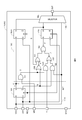
- FIG. 1 is a diagram showing a configuration of a register circuit 100A according to an embodiment of the present invention.
- the register circuit 100A is a circuit that stores 1-bit data (0 or 1).
- a plurality of register circuits can be formed using a plurality of register circuits 100A.
- the register circuit 100A can be used to hold transfer data in a data transfer interface such as MIPI. Note that the use of the register circuit 100A is not limited to this.
- the register circuit 100A includes terminals VCC, CLK, RES, WR, IN, GND, and OUT.
- the register circuit 100 ⁇ / b> A includes an initial value wiring 110, D flip-flops (hereinafter simply referred to as “flip-flops”) 120 and 130, a selector 140, and an output control circuit 150.
- a power supply voltage for driving the register circuit 100A is supplied to the terminal VCC (power supply terminal).
- a clock signal used for the operation of the register circuit 100A is input to the terminal CLK.
- a reset signal for resetting the flip-flops 120 and 130 is input to the terminal RES.
- a write signal for instructing data writing to the register circuit 100A is input to the terminal WR.
- An input signal (0 or 1) for writing to the register circuit 100A is input to the terminal IN.
- a ground potential is supplied to the terminal GND (ground terminal).
- An output signal having a value stored in the register circuit 100A is output from the terminal OUT.
- FIG. 1 the connection relationship between a terminal and each element is shown simply.
- the terminal VCC is connected to each element to supply a power supply voltage, but is omitted in FIG.
- the terminal GND is connected to each element to supply a ground potential, but is omitted in FIG.
- the initial value INIT of the register circuit 100A is supplied to the initial value wiring 110.
- the initial value wiring 110 is connected to the terminal VCC. That is, the initial value INIT is set to 1 in the register circuit 100A.
- the flip-flop 120 (first flip-flop) includes a data input terminal D, a clock terminal C, a data output terminal Q, an inverted data output terminal / Q, and a reset terminal R.
- the flip-flop 120 when the reset signal becomes 1 (high level), the output of the data output terminal Q is reset to 0 and the output of the inverted data output terminal / Q is reset to 1.
- the power supply voltage (value 1) is input to the data input terminal D, and the clock signal is inverted and input to the clock terminal C. Therefore, the value 1 is latched at the falling timing of the clock signal, the output of the data output terminal Q changes to 1, and the output (first signal) of the inverted data output terminal / Q changes to 0.
- the flip-flop 130 (second flip-flop) includes a data input terminal D, a clock terminal C, a data output terminal Q, a data inversion output terminal / Q, and a reset terminal R.
- the flip-flop 130 when the reset signal becomes 1 (high level), the output of the data output terminal Q is reset to 0 and the output of the inverted data output terminal / Q is reset to 1.
- the signal F (second signal) output from the output control circuit 150 is input to the data input terminal D, and the clock signal is inverted and input to the clock terminal C. Therefore, the value of the signal F is latched at the falling timing of the clock signal, and the output of the data output terminal Q changes to the value of the signal F.
- the selector 140 outputs the initial value INIT or the output of the data output terminal Q of the flip-flop 130 as an output signal based on the selection signal SEL.
- the output of the data output terminal Q of the flip-flop 120 is input to the selector 140 as the selection signal SEL.
- the selector 140 outputs the initial value INIT as an output signal, and the output of the data output terminal Q of the flip-flop 120 is 1. In this case, the output of the data output terminal Q of the flip-flop 130 is output as an output signal.
- the selector 140 outputs the initial value INIT as an output signal before the change of the output (first signal) of the inverted data output terminal / Q of the flip-flop 120, and the inverted data output terminal / Q of the flip-flop 120. After the change of the output (first signal), the output of the data output terminal Q of the flip-flop 130 is output as an output signal.
- the output control circuit 150 is a logic circuit that outputs an initial value INIT or an input signal from the terminal IN as a signal F (second signal). Specifically, the output control circuit 150 outputs the initial value INIT as the signal F (second signal) before the output (first signal) of the inverted data output terminal / Q of the flip-flop 120 changes. After the change of the output (first signal) of the inverted data output terminal / Q of the flip-flop 120, the input signal is output as the signal F (second signal) according to the write signal.
- the output control circuit 150 can be configured using, for example, AND circuits 151 to 153, a NAND circuit 154, an OR circuit 155, and NOR circuits 156 and 157.
- the AND circuit 151 receives the output (signal A) of the data output terminal Q of the flip-flop 120 and the write signal. Therefore, the AND circuit 151 outputs a signal C indicating the logical product of the signal A and the write signal.
- the initial value INIT and the inverted data output / Q output (signal B) of the flip-flop 120 are input to the AND circuit 152. Therefore, the AND circuit 152 outputs a signal indicating the logical product of the initial value INIT and the signal B.
- the AND circuit 153 receives the signal C from the AND circuit 151 and the input signal from the terminal IN. Therefore, the AND circuit 153 outputs a signal indicating the logical product of the signal C and the input signal.
- the NOR circuit 156 receives the signal C from the AND circuit 151 and the inverted data output / Q output (signal B) of the flip-flop 120. Therefore, the NOR circuit 156 outputs a signal indicating the negative logical sum of the signal C and the signal B.
- the OR circuit 155 In the OR circuit 155, the output (signal Q) of the data output terminal Q of the flip-flop 130 and the output of the NOR circuit 156 are inverted and input. Therefore, the OR circuit 155 outputs a signal indicating the logical sum of the inverted signal of the signal Q and the inverted signal of the output of the NOR circuit 156.
- the outputs of the AND circuits 152 and 153 are input to the NOR circuit 157. Therefore, the NOR circuit 157 outputs a signal D indicating the negative logical sum of the outputs of the AND circuits 152 and 153.
- the NAND circuit 154 receives the output of the OR circuit 155 and the output of the NOR circuit 157. Accordingly, the NAND circuit 154 outputs a signal F indicating a negative logical product of the output of the OR circuit 155 and the output of the NOR circuit 157 (signal D).
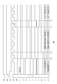
- FIG. 2 is a timing chart showing an example of the operation of the register circuit 100A.
- the input signal from the terminal IN is 0 (fixed value).
- the initial value INIT supplied to the initial value wiring 110 becomes a value 1 corresponding to the power supply voltage.
- the output (signal A) of the data output terminal Q becomes 0 and the output (signal B) of the inverted data output terminal / Q becomes 1 due to the reset signal. Therefore, the selector 140 outputs the initial value INIT (1) of the initial value wiring 110 from the terminal OUT.
- the output (signal Q) of the data output terminal Q of the flip-flop 130 is 0 by the reset signal.
- the output (signal F) of the output control circuit 150 is a value 1 corresponding to the initial value INIT.
- the flip-flop 120 latches the value 1 corresponding to the power supply voltage at the first falling edge (time T1). As a result, in the flip-flop 120, the output of the data output terminal Q (signal A) changes to 1, and the output of the inverted data output terminal / Q (signal B) changes to 0.
- the flip-flop 130 latches the value 1 of the signal F.
- the output (signal Q) of the data output terminal Q of the flip-flop 130 becomes the initial value INIT (1) read from the initial value wiring 110. Since the signal A is 1, the selector 140 outputs the signal Q (1) from the terminal OUT.
- the output (signal C) of the AND circuit 151 changes to 1.
- the output (signal E) of the NOR circuit 156 changes to 0, and the output (signal F) of the NAND circuit 154 changes to 0 (value 0 of the input signal from the terminal IN).
- the flip-flop 130 latches the value 0 of the signal F (the value 0 of the input signal from the terminal IN).
- the output (signal Q) of the data output terminal Q of the flip-flop 130 becomes the value 0 of the input signal from the terminal IN.
- the selector 140 outputs the signal Q (0) from the terminal OUT.
- the value (0 or 1) of the input signal is latched in the flip-flop 130 in accordance with the write signal and output from the terminal OUT.
- the value 1 supplied to the initial value wiring 110 can be set as the initial value. Therefore, according to the register circuit 100A, a register circuit having an initial value as a value supplied to the initial value wiring 110 can be configured without using a flip-flop having both a set terminal and a reset terminal.
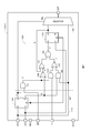
- FIG. 3 is a diagram showing a configuration of a register circuit 100B according to another embodiment of the present invention.
- the register circuit 100B is the same as the register circuit 100A except that the initial value wiring 110 is connected to the terminal GND.
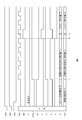
- FIG. 4 is a timing chart showing an example of the operation of the register circuit 100B.
- the input signal from the terminal IN is 1 (fixed value).
- the operation of the register circuit 100B will be described while appropriately omitting the same operation as that of the register circuit 100A.
- the initial value INIT supplied to the initial value wiring 110 is a value 0 (fixed value) corresponding to the ground potential. Therefore, the selector 140 outputs the initial value INIT (0) of the initial value wiring 110 from the terminal OUT. At this time, the output (signal F) of the output control circuit 150 has a value 0 corresponding to the initial value INIT.
- the flip-flop 120 latches the value 1 corresponding to the power supply voltage at the first falling edge (time T1). As a result, in the flip-flop 120, the output of the data output terminal Q (signal A) changes to 1, and the output of the inverted data output terminal / Q (signal B) changes to 0.
- the flip-flop 130 latches the value 0 of the signal F.
- the output (signal Q) of the data output terminal Q of the flip-flop 130 becomes the initial value INIT (0) read from the initial value wiring 110.
- the selector 140 outputs the signal Q (0) from the terminal OUT.
- the output (signal F) of the NAND circuit 154 changes to 1 (value 1 of the input signal from the terminal IN).
- the flip-flop 130 latches the value 1 of the signal F (the value 1 of the input signal from the terminal IN).
- the output (signal Q) of the data output terminal Q of the flip-flop 130 becomes the value 1 of the input signal from the terminal IN.
- the selector 140 outputs the signal Q (1) from the terminal OUT.
- the value (0 or 1) of the input signal is latched in the flip-flop 130 in accordance with the write signal and output from the terminal OUT.
- the register circuit 100B it is possible to configure a register circuit that uses the value 0 set in the initial value wiring 110 as an initial value without using a flip-flop having both a set terminal and a reset terminal. it can.
- the initial value INIT set to the initial value wiring 110 by changing the initial value INIT set to the initial value wiring 110, the initial value can be changed without using a flip-flop having both a set terminal and a reset terminal.
- a register circuit can be provided.
- FIG. 5 is a diagram showing a configuration of a register circuit 100C according to another embodiment of the present invention. The same elements as those in the register circuit 100A shown in FIG.
- the register circuit 100C includes a flip-flop 500 in addition to the configuration of the register circuit 100A.
- the flip-flop 500 (third flip-flop) includes a data input terminal D, a clock terminal C, a data output terminal Q, a data inversion output terminal / Q, and a reset terminal R.
- the flip-flop 500 when the reset signal becomes 1 (high level), the output of the data output terminal Q is reset to 0 and the output of the inverted data output terminal / Q is reset to 1.
- the output (signal A) of the data output terminal Q of the flip-flop 120 is input to the data input terminal D, and the clock signal is inverted and input to the clock terminal C.
- the value of the signal A (third signal) is latched at the falling timing of the clock signal, and the output (fourth signal) of the data output terminal Q changes to the value of the signal A. Then, the output of the data output terminal Q of the flip-flop 500 is supplied to the selector 140 as the selection signal SEL.
- FIG. 6 is a timing chart showing an example of the operation of the register circuit 100C.
- the input signal from the terminal IN is 0 (fixed value).
- the operation of the register circuit 100C will be described while omitting the operations similar to those of the register circuit 100A as appropriate.
- the flip-flop 120 latches the value 1 corresponding to the power supply voltage at the first fall (time T1-1). As a result, in the flip-flop 120, the output of the data output terminal Q (signal A) changes to 1, and the output of the inverted data output terminal / Q (signal B) changes to 0.
- the flip-flop 130 latches the value 1 of the signal F.
- the output (signal Q) of the data output terminal Q of the flip-flop 130 becomes the initial value INIT (1) read from the initial value wiring 110.
- the output (signal SEL) of the data output terminal Q of the flip-flop 500 is the reset initial value 0. Therefore, the selector 140 outputs the initial value INIT (1) of the initial value wiring 110 from the terminal OUT.
- the flip-flop 500 latches the value 1 of the output (signal A) of the data output terminal Q.
- the output (signal SEL) of the data output terminal Q of the flip-flop 500 changes to 1.
- the selector 140 outputs the value 1 (the value 1 read from the initial value wiring 110) of the output (signal Q) of the data output terminal Q of the flip-flop 130 from the terminal OUT.
- the register circuit 100C it is possible to configure a register circuit that uses the value 1 set in the initial value wiring 110 as an initial value without using a flip-flop having both a set terminal and a reset terminal. it can.
- the flip-flop 500 since the flip-flop 500 is provided, the latch timing (T1-1) of the flip-flop 130 and the switching timing (T1-2) of the selector 140 can be shifted. This makes it possible to suppress noise when the selector 140 is switched.
- FIG. 7 is a diagram showing a configuration of a register circuit 100D according to another embodiment of the present invention.
- the register circuit 100D is the same as the register circuit 100A except that the clock signal is input to the clock terminals C of the flip-flops 120 and 130 without being inverted.
- FIG. 8 is a timing chart showing an example of the operation of the register circuit 100D.
- the input signal from the terminal IN is 1 (fixed value).
- the operation of the register circuit 100D will be described while appropriately omitting the same operation as that of the register circuit 100A.
- the flip-flop 120 latches the value 1 corresponding to the power supply voltage at the first rise (time T1). As a result, in the flip-flop 120, the output of the data output terminal Q (signal A) changes to 1, and the output of the inverted data output terminal / Q (signal B) changes to 0.
- the flip-flop 130 latches the value 1 of the signal F.
- the output (signal Q) of the data output terminal Q of the flip-flop 130 becomes the initial value INIT (1) read from the initial value wiring 110. Since the signal A is 1, the selector 140 outputs the signal Q (1) from the terminal OUT.
- the output (signal F) of the NAND circuit 154 changes to 0 (value 0 of the input signal from the terminal IN).
- the flip-flop 130 latches the value 0 of the signal F (the value 0 of the input signal from the terminal IN).
- the output (signal Q) of the data output terminal Q of the flip-flop 130 becomes the value 0 of the input signal from the terminal IN.
- the selector 140 outputs the signal Q (0) from the terminal OUT.
- the value (0 or 1) of the input signal is latched in the flip-flop 130 in accordance with the write signal and output from the terminal OUT.
- the register circuit 100D it is possible to configure a register circuit having a value 1 set to the initial value wiring 110 as an initial value without using a flip-flop having both a set terminal and a reset terminal. it can.
- the register circuit 100B by connecting the initial value wiring 110 of the register circuit 100D to the terminal GND, it is possible to configure a register circuit having the value 0 set in the initial value wiring 110 as an initial value. is there.
- the register circuit 100C can also be configured to be latched at the rising edge of the clock, as in the register circuit 100D.
- register circuits 100A to 100D it is possible to provide a register circuit that can change an initial value by using a flip-flop having both a set terminal and a reset terminal by changing a value set in the initial value wiring 110. can do.
- a flip-flop having a reset terminal is used, but a flip-flop having a set terminal can also be used.
- the register circuit 100C includes the flip-flop 500 (third flip-flop), so that the latch timing of the flip-flop 130 and the switching timing of the selector 140 can be shifted. This makes it possible to suppress noise when the selector 140 is switched.
- the value set in the initial value wiring 110 can be changed by setting the connection destination of the initial value wiring 110 to the terminal VCC or the terminal GND.
- the initial value of the register circuit can be changed by changing the connection of the initial value wiring 110.
- a terminal for inputting a value set in the initial value wiring 110 may be provided separately.
- each embodiment described above is for facilitating the understanding of the present invention, and is not intended to limit the present invention.
- the present invention can be changed / improved without departing from the spirit thereof, and the present invention includes equivalents thereof.
- those obtained by appropriately modifying the design of each embodiment by those skilled in the art are also included in the scope of the present invention as long as they include the features of the present invention.
- each element included in each embodiment and its arrangement, material, condition, shape, size, and the like are not limited to those illustrated, and can be changed as appropriate.
- each element included in each embodiment can be combined as much as technically possible, and combinations thereof are included in the scope of the present invention as long as they include the features of the present invention.
Landscapes
- Engineering & Computer Science (AREA)
- Physics & Mathematics (AREA)
- General Engineering & Computer Science (AREA)
- Computer Hardware Design (AREA)
- Computing Systems (AREA)
- Mathematical Physics (AREA)
- Power Engineering (AREA)
- General Physics & Mathematics (AREA)
- Logic Circuits (AREA)
Abstract
セット端子及びリセット端子の両方を有するフリップフロップを用いることなく、初期値を変更可能なレジスタ回路を提供する。レジスタ回路は、クロック信号の入力に応じて、第1の信号を第1の値から第2の値に変化させる第1のフリップフロップと、前記第1の信号が前記第1の値の場合に、初期値配線から供給される出力信号の初期値を第2の信号として出力し、前記第1の信号が前記第2の値の場合に、入力信号の書き込みを指示するライト信号に応じて前記入力信号を前記第2の信号として出力する出力制御回路と、前記クロック信号に基づいて前記第2の信号をラッチして出力する第2のフリップフロップと、前記第1の信号が前記第1の値の場合に、前記初期値を前記出力信号として出力し、前記第1の信号が前記第2の値の場合に、前記第2のフリップフロップから供給される前記第2の信号を前記出力信号として出力するセレクタと、を備える。
Description
本発明は、レジスタ回路に関する。
入力信号を記憶するレジスタ回路は、様々な電子機器において用いられている。例えば、MIPI(Mobile Industry Processor Interface)等のデータ転送インタフェースにおいて、転送データを保持するためにレジスタ回路が用いられる(例えば、特許文献1)。
レジスタ回路の初期値は、レジスタ回路が用いられる電子機器の仕様に応じて決定される。従って、例えば、1ビットのレジスタ回路の初期値は、0である場合もあるし、1である場合もある。このように、初期値を0または1に設定することが可能なレジスタ回路は、例えば、セット端子及びリセット端子を有するフリップフロップを用いて構成することができる。しかしながら、レジスタ回路を設計する際のスタンダードセルライブラリには、セット端子及びリセット端子の両方を有するフリップフロップが用意されていない場合もある。
本発明はこのような事情に鑑みてなされたものであり、セット端子及びリセット端子の両方を有するフリップフロップを用いることなく、初期値を変更可能なレジスタ回路を提供することを目的とする。
本発明の一側面に係るレジスタ回路は、入力信号が入力され、出力信号を出力するレジスタ回路であって、前記出力信号の初期値を供給するための初期値配線と、前記入力信号が入力される入力端子と、前記入力信号の書き込みを指示するライト信号が入力されるライト信号端子と、クロック信号が入力されるクロック信号端子と、前記クロック信号の入力に応じて、第1の信号を第1の値から第2の値に変化させる第1のフリップフロップと、前記第1の信号が前記第1の値の場合に、前記初期値を第2の信号として出力し、前記第1の信号が前記第2の値の場合に、前記ライト信号に応じて前記入力信号を前記第2の信号として出力する出力制御回路と、前記クロック信号に基づいて前記第2の信号をラッチして出力する第2のフリップフロップと、前記第1の信号が前記第1の値の場合に、前記初期値配線から供給される前記初期値を前記出力信号として出力し、前記第1の信号が前記第2の値の場合に、前記第2のフリップフロップから供給される前記第2の信号を前記出力信号として出力するセレクタと、を備える。
本発明によれば、セット端子及びリセット端子の両方を有するフリップフロップを用いることなく、初期値を変更可能なレジスタ回路を提供することができる。
以下、図面を参照して本発明の一実施形態について説明する。図1は、本発明の一実施形態であるレジスタ回路100Aの構成を示す図である。レジスタ回路100Aは、1ビットのデータ(0または1)を記憶する回路である。複数のレジスタ回路100Aを用いて、複数ビットのレジスタ回路を構成することも可能である。レジスタ回路100Aは、例えば、MIPI等のデータ転送インタフェースにおいて、転送データを保持するために用いることができる。なお、レジスタ回路100Aの用途はこれに限られない。
図1に示すように、レジスタ回路100Aは、端子VCC,CLK,RES,WR,IN,GND,OUTを備える。また、レジスタ回路100Aは、初期値配線110、Dフリップフロップ(以下、単に「フリップフロップ」という。)120,130、セレクタ140、及び出力制御回路150を備える。
端子VCC(電源端子)には、レジスタ回路100Aを駆動するための電源電圧が供給される。端子CLKには、レジスタ回路100Aの動作に用いられるクロック信号が入力される。端子RESには、フリップフロップ120,130をリセットするためのリセット信号が入力される。端子WRには、レジスタ回路100Aへのデータの書き込みを指示するライト信号が入力される。端子INには、レジスタ回路100Aに書き込むための入力信号(0または1)が入力される。端子GND(接地端子)には、接地電位が供給される。端子OUTからは、レジスタ回路100Aに記憶されている値を有する出力信号が出力される。なお、図1では、端子と各要素との接続関係が簡略的に示されている。例えば、端子VCCは、電源電圧を供給するために各要素と接続されるが、図1においては省略されている。また、例えば、端子GNDは、接地電位を供給するために各要素と接続されるが、図1においては省略されている。
初期値配線110には、レジスタ回路100Aの初期値INITが供給される。レジスタ回路100Aでは、初期値配線110は、端子VCCに接続されている。即ち、レジスタ回路100Aでは、初期値INITが1に設定されている。
フリップフロップ120(第1のフリップフロップ)は、データ入力端子D、クロック端子C、データ出力端子Q、反転データ出力端子/Q、及びリセット端子Rを備える。フリップフロップ120では、リセット信号が1(ハイレベル)となることにより、データ出力端子Qの出力が0、反転データ出力端子/Qの出力が1にリセットされる。また、フリップフロップ120では、データ入力端子Dに電源電圧(値1)が入力され、クロック端子Cにクロック信号が反転入力される。従って、クロック信号の立ち下がりのタイミングで、値1がラッチされ、データ出力端子Qの出力が1に変化し、反転データ出力端子/Qの出力(第1の信号)が0に変化する。
フリップフロップ130(第2のフリップフロップ)は、データ入力端子D、クロック端子C、データ出力端子Q、データ反転出力端子/Q、及びリセット端子Rを備える。フリップフロップ130では、リセット信号が1(ハイレベル)となることにより、データ出力端子Qの出力が0、反転データ出力端子/Qの出力が1にリセットされる。また、フリップフロップ130では、データ入力端子Dに、出力制御回路150から出力される信号F(第2の信号)が入力され、クロック端子Cにクロック信号が反転入力される。従って、クロック信号の立ち下がりのタイミングで、信号Fの値がラッチされ、データ出力端子Qの出力が信号Fの値に変化する。
セレクタ140は、選択信号SELに基づいて、初期値INITまたはフリップフロップ130のデータ出力端子Qの出力を、出力信号として出力する。レジスタ回路100Aでは、フリップフロップ120のデータ出力端子Qの出力が、選択信号SELとしてセレクタ140に入力されている。そして、セレクタ140は、フリップフロップ120のデータ出力端子Qの出力が0(リセットされた値)の場合は、初期値INITを出力信号として出力し、フリップフロップ120のデータ出力端子Qの出力が1の場合は、フリップフロップ130のデータ出力端子Qの出力を出力信号として出力する。即ち、セレクタ140は、フリップフロップ120の反転データ出力端子/Qの出力(第1の信号)の変化の前は、初期値INITを出力信号として出力し、フリップフロップ120の反転データ出力端子/Qの出力(第1の信号)の変化の後は、フリップフロップ130のデータ出力端子Qの出力を出力信号として出力する。
出力制御回路150は、初期値INITまたは端子INからの入力信号を信号F(第2の信号)として出力する論理回路である。具体的には、出力制御回路150は、フリップフロップ120の反転データ出力端子/Qの出力(第1の信号)の変化の前は、初期値INITを信号F(第2の信号)として出力し、フリップフロップ120の反転データ出力端子/Qの出力(第1の信号)の変化の後は、ライト信号に応じて、入力信号を信号F(第2の信号)として出力する。
図1に示すように、出力制御回路150は、例えば、AND回路151~153、NAND回路154、OR回路155、及びNOR回路156,157を用いて構成することができる。
AND回路151には、フリップフロップ120のデータ出力端子Qの出力(信号A)と、ライト信号とが入力されている。従って、AND回路151は、信号A及びライト信号の論理積を示す信号Cを出力する。
AND回路152には、初期値INITと、フリップフロップ120の反転データ出力/Qの出力(信号B)とが入力されている。従って、AND回路152は、初期値INIT及び信号Bの論理積を示す信号を出力する。
AND回路153には、AND回路151からの信号Cと、端子INからの入力信号とが入力されている。従って、AND回路153は、信号C及び入力信号の論理積を示す信号を出力する。
NOR回路156には、AND回路151からの信号Cと、フリップフロップ120の反転データ出力/Qの出力(信号B)とが入力されている。従って、NOR回路156は、信号C及び信号Bの否定論理和を示す信号を出力する。
OR回路155には、フリップフロップ130のデータ出力端子Qの出力(信号Q)と、NOR回路156の出力とが反転入力されている。従って、OR回路155は、信号Qの反転信号と、NOR回路156の出力の反転信号との論理和を示す信号を出力する。
NOR回路157には、AND回路152,153の出力が入力されている。従って、NOR回路157は、AND回路152,153の出力の否定論理和を示す信号Dを出力する。
NAND回路154には、OR回路155の出力と、NOR回路157の出力とが入力されている。従って、NAND回路154は、OR回路155の出力と、NOR回路157(信号D)の出力との否定論理積を示す信号Fを出力する。
なお、図1に示す出力制御回路150の論理回路の構成は一例であり、同様の論理を実現する任意の構成を採用することができる。
図2は、レジスタ回路100Aの動作の一例を示すタイミングチャートである。なお、図2に示すタイミングチャートでは、端子INからの入力信号は0(固定値)となっている。
レジスタ回路100Aの動作が開始すると、初期値配線110に供給される初期値INITは、電源電圧に応じた値1になる。また、フリップフロップ120では、リセット信号により、データ出力端子Qの出力(信号A)が0となり、反転データ出力端子/Qの出力(信号B)が1となっている。従って、セレクタ140は、初期値配線110の初期値INIT(1)を端子OUTから出力する。
このとき、フリップフロップ130のデータ出力端子Qの出力(信号Q)は、リセット信号により0となっている。また、出力制御回路150の出力(信号F)は、初期値INITに応じた値1となっている。
その後、クロック信号が入力されると、1つ目の立ち下がり(時刻T1)で、フリップフロップ120は、電源電圧に応じた値1をラッチする。これにより、フリップフロップ120では、データ出力端子Qの出力(信号A)が1に変化し、反転データ出力端子/Qの出力(信号B)が0に変化する。
また、フリップフロップ130は、信号Fの値1をラッチする。これにより、フリップフロップ130のデータ出力端子Qの出力(信号Q)は、初期値配線110から読み込まれた初期値INIT(1)となる。そして、信号Aが1であるため、セレクタ140は、信号Q(1)を端子OUTから出力する。
時刻T1において、ライト信号は0であるため、AND回路151の出力(信号C)は0のままである。また、信号Bが0に変化したことにより、NOR回路157の出力(信号D)は1に変化し、NOR回路156の出力(信号E)は1に変化する。そして、信号Q及び信号Eが1であるため、信号Fは1(初期値INITの値1)となる。その後、ライト信号が入力されるまでは、この状態が継続される。
時刻T2に、端子WRからのライト信号が1になると、AND回路151の出力(信号C)が1に変化する。これにより、NOR回路156の出力(信号E)が0に変化し、NAND回路154の出力(信号F)が0(端子INからの入力信号の値0)に変化する。その後のクロック信号の立ち下がり(時刻T3)で、フリップフロップ130は、信号Fの値0(端子INからの入力信号の値0)をラッチする。これにより、フリップフロップ130のデータ出力端子Qの出力(信号Q)は、端子INからの入力信号の値0となる。そして、セレクタ140は、信号Q(0)を端子OUTから出力する。
以後同様に、ライト信号に応じて、入力信号の値(0または1)がフリップフロップ130にラッチされ、端子OUTから出力される。
以上のように、レジスタ回路100Aでは、初期値配線110に供給される値1を初期値とすることができる。従って、レジスタ回路100Aによれば、セット端子及びリセット端子の両方を有するフリップフロップを用いることなく、初期値配線110に供給される値を初期値とするレジスタ回路を構成することができる。
図3は、本発明の他の実施形態であるレジスタ回路100Bの構成を示す図である。なお、図1に示したレジスタ回路100Aと同一の要素には同一の符号を付して説明を省略する。レジスタ回路100Bは、初期値配線110が端子GNDに接続されている点を除き、レジスタ回路100Aと同一である。
図4は、レジスタ回路100Bの動作の一例を示すタイミングチャートである。なお、図4に示すタイミングチャートでは、端子INからの入力信号は1(固定値)となっている。以下、レジスタ回路100Aと同様の動作については適宜省略しつつ、レジスタ回路100Bの動作を説明する。
レジスタ回路100Bでは、初期値配線110が端子GNDに接続されているため、初期値配線110に供給される初期値INITは、接地電位に応じた値0(固定値)である。従って、セレクタ140は、初期値配線110の初期値INIT(0)を端子OUTから出力する。このとき、出力制御回路150の出力(信号F)は、初期値INITに応じた値0となっている。
その後、クロック信号が入力されると、1つ目の立ち下がり(時刻T1)で、フリップフロップ120は、電源電圧に応じた値1をラッチする。これにより、フリップフロップ120では、データ出力端子Qの出力(信号A)が1に変化し、反転データ出力端子/Qの出力(信号B)が0に変化する。
また、フリップフロップ130は、信号Fの値0をラッチする。これにより、フリップフロップ130のデータ出力端子Qの出力(信号Q)は、初期値配線110から読み込まれた初期値INIT(0)となる。そして、信号Aが1となったことにより、セレクタ140は、信号Q(0)を端子OUTから出力する。
時刻T2に、端子WRからのライト信号が1になると、NAND回路154の出力(信号F)が1(端子INからの入力信号の値1)に変化する。その後のクロック信号の立ち下がり(時刻T3)で、フリップフロップ130は、信号Fの値1(端子INからの入力信号の値1)をラッチする。これにより、フリップフロップ130のデータ出力端子Qの出力(信号Q)は、端子INからの入力信号の値1となる。そして、セレクタ140は、信号Q(1)を端子OUTから出力する。
以後同様に、ライト信号に応じて、入力信号の値(0または1)がフリップフロップ130にラッチされ、端子OUTから出力される。
以上のように、レジスタ回路100Bによれば、セット端子及びリセット端子の両方を有するフリップフロップを用いることなく、初期値配線110に設定された値0を初期値とするレジスタ回路を構成することができる。
図1~図4に示したように、初期値配線110に設定される初期値INITを変更することにより、セット端子及びリセット端子の両方を有するフリップフロップを用いることなく、初期値を変更可能なレジスタ回路を提供することができる。
図5は、本発明の他の実施形態であるレジスタ回路100Cの構成を示す図である。なお、図1に示したレジスタ回路100Aと同一の要素には同一の符号を付して説明を省略する。レジスタ回路100Cは、レジスタ回路100Aの構成に加えて、フリップフロップ500を備える。
フリップフロップ500(第3のフリップフロップ)は、データ入力端子D、クロック端子C、データ出力端子Q、データ反転出力端子/Q、及びリセット端子Rを備える。フリップフロップ500では、リセット信号が1(ハイレベル)となることにより、データ出力端子Qの出力が0、反転データ出力端子/Qの出力が1にリセットされる。また、フリップフロップ500では、データ入力端子Dに、フリップフロップ120のデータ出力端子Qの出力(信号A)が入力され、クロック端子Cにクロック信号が反転入力される。従って、クロック信号の立ち下がりのタイミングで、信号A(第3の信号)の値がラッチされ、データ出力端子Qの出力(第4の信号)が信号Aの値に変化する。そして、フリップフロップ500のデータ出力端子Qの出力が、選択信号SELとして、セレクタ140に供給される。
図6は、レジスタ回路100Cの動作の一例を示すタイミングチャートである。なお、図6に示すタイミングチャートでは、端子INからの入力信号は0(固定値)となっている。以下、レジスタ回路100Aと同様の動作については適宜省略しつつ、レジスタ回路100Cの動作を説明する。
レジスタ回路100Cの動作が開始され、クロック信号が入力されると、1つ目の立ち下がり(時刻T1-1)で、フリップフロップ120は、電源電圧に応じた値1をラッチする。これにより、フリップフロップ120では、データ出力端子Qの出力(信号A)が1に変化し、反転データ出力端子/Qの出力(信号B)が0に変化する。
また、フリップフロップ130は、信号Fの値1をラッチする。これにより、フリップフロップ130のデータ出力端子Qの出力(信号Q)は、初期値配線110から読み込まれた初期値INIT(1)となる。このとき、フリップフロップ500のデータ出力端子Qの出力(信号SEL)は、リセットされた初期値0である。従って、セレクタ140は、初期値配線110の初期値INIT(1)を端子OUTから出力する。
続いて、クロック信号の次の立ち下がり(時刻T1-2)で、フリップフロップ500は、データ出力端子Qの出力(信号A)の値1をラッチする。これにより、フリップフロップ500のデータ出力端子Qの出力(信号SEL)は1に変化する。従って、セレクタ140は、フリップフロップ130のデータ出力端子Qの出力(信号Q)の値1(初期値配線110から読み込まれた値1)を端子OUTから出力する。
以後は、レジスタ回路100Aと同様の動作であるため説明を省略する。
以上のように、レジスタ回路100Cによれば、セット端子及びリセット端子の両方を有するフリップフロップを用いることなく、初期値配線110に設定された値1を初期値とするレジスタ回路を構成することができる。また、レジスタ回路100Cでは、フリップフロップ500が設けられていることにより、フリップフロップ130のラッチのタイミング(T1-1)と、セレクタ140の切り替えのタイミング(T1-2)とをずらすことができる。これにより、セレクタ140の切り替え時のノイズを抑制することが可能となる。
なお、レジスタ回路100Bと同様に、レジスタ回路100Cの初期値配線110を端子GNDに接続することにより、初期値配線110に設定された値0を初期値とするレジスタ回路を構成することが可能である。
図7は、本発明の他の実施形態であるレジスタ回路100Dの構成を示す図である。なお、図1に示したレジスタ回路100Aと同一の要素には同一の符号を付して説明を省略する。レジスタ回路100Dは、フリップフロップ120,130のクロック端子Cにクロック信号が反転されずに入力される点を除き、レジスタ回路100Aと同一である。
図8は、レジスタ回路100Dの動作の一例を示すタイミングチャートである。なお、図8に示すタイミングチャートでは、端子INからの入力信号は1(固定値)となっている。以下、レジスタ回路100Aと同様の動作については適宜省略しつつ、レジスタ回路100Dの動作を説明する。
レジスタ回路100Dの動作が開始され、クロック信号が入力されると、1つ目の立ち上がり(時刻T1)で、フリップフロップ120は、電源電圧に応じた値1をラッチする。これにより、フリップフロップ120では、データ出力端子Qの出力(信号A)が1に変化し、反転データ出力端子/Qの出力(信号B)が0に変化する。
また、フリップフロップ130は、信号Fの値1をラッチする。これにより、フリップフロップ130のデータ出力端子Qの出力(信号Q)は、初期値配線110から読み込まれた初期値INIT(1)となる。そして、信号Aが1であるため、セレクタ140は、信号Q(1)を端子OUTから出力する。
時刻T2に、端子WRからのライト信号が1になると、NAND回路154の出力(信号F)が0(端子INからの入力信号の値0)に変化する。その後のクロック信号の立ち上がり(時刻T3)で、フリップフロップ130は、信号Fの値0(端子INからの入力信号の値0)をラッチする。これにより、フリップフロップ130のデータ出力端子Qの出力(信号Q)は、端子INからの入力信号の値0となる。そして、セレクタ140は、信号Q(0)を端子OUTから出力する。
以後同様に、ライト信号に応じて、入力信号の値(0または1)がフリップフロップ130にラッチされ、端子OUTから出力される。
以上のように、レジスタ回路100Dによれば、セット端子及びリセット端子の両方を有するフリップフロップを用いることなく、初期値配線110に設定された値1を初期値とするレジスタ回路を構成することができる。
なお、レジスタ回路100Bと同様に、レジスタ回路100Dの初期値配線110を端子GNDに接続することにより、初期値配線110に設定された値0を初期値とするレジスタ回路を構成することが可能である。また、レジスタ回路100Cについても、レジスタ回路100Dと同様に、クロックの立ち上がりでラッチが行われる構成とすることができる。
以上、本発明のいくつかの実施形態について説明した。レジスタ回路100A~100Dによれば、初期値配線110に設定される値を変更することにより、セット端子及びリセット端子の両方を有するフリップフロップを用いることなく、初期値を変更可能なレジスタ回路を提供することができる。
なお、レジスタ回路100A~100Dでは、リセット端子を有するフリップフロップが用いられているが、セット端子を有するフリップフロップを用いることも可能である。
また、レジスタ回路100Cでは、フリップフロップ500(第3のフリップフロップ)を備えることにより、フリップフロップ130のラッチのタイミングと、セレクタ140の切り替えのタイミングとをずらすことができる。これにより、セレクタ140の切り替え時のノイズを抑制することが可能となる。
また、レジスタ回路100A~100Dでは、初期値配線110の接続先を端子VCCまたは端子GNDにすることにより、初期値配線110に設定される値を変更することができる。これにより、初期値配線110の接続変更によって、レジスタ回路の初期値を変更することができる。なお、初期値配線110に設定される値が入力される端子が別途設けられてもよい。
以上説明した各実施形態は、本発明の理解を容易にするためのものであり、本発明を限定して解釈するためのものではない。本発明は、その趣旨を逸脱することなく、変更/改良され得るととともに、本発明にはその等価物も含まれる。即ち、各実施形態に当業者が適宜設計変更を加えたものも、本発明の特徴を備えている限り、本発明の範囲に包含される。例えば、各実施形態が備える各要素およびその配置、材料、条件、形状、サイズなどは、例示したものに限定されるわけではなく適宜変更することができる。また、各実施形態が備える各要素は、技術的に可能な限りにおいて組み合わせることができ、これらを組み合わせたものも本発明の特徴を含む限り本発明の範囲に包含される。
100A,100B,100C,100D レジスタ回路
110 初期値配線
120,130,500 フリップフロップ
140 セレクタ
150 出力制御回路
151~153 AND回路
154 NAND回路
155 OR回路
156,157 NOR回路
110 初期値配線
120,130,500 フリップフロップ
140 セレクタ
150 出力制御回路
151~153 AND回路
154 NAND回路
155 OR回路
156,157 NOR回路
Claims (3)
- 入力信号が入力され、出力信号を出力するレジスタ回路であって、
前記出力信号の初期値を供給するための初期値配線と、
前記入力信号が入力される入力端子と、
前記入力信号の書き込みを指示するライト信号が入力されるライト信号端子と、
クロック信号が入力されるクロック信号端子と、
前記クロック信号の入力に応じて、第1の信号を第1の値から第2の値に変化させる第1のフリップフロップと、
前記第1の信号が前記第1の値の場合に、前記初期値を第2の信号として出力し、前記第1の信号が前記第2の値の場合に、前記ライト信号に応じて前記入力信号を前記第2の信号として出力する出力制御回路と、
前記クロック信号に基づいて前記第2の信号をラッチして出力する第2のフリップフロップと、
前記第1の信号が前記第1の値の場合に、前記初期値配線から供給される前記初期値を前記出力信号として出力し、前記第1の信号が前記第2の値の場合に、前記第2のフリップフロップから供給される前記第2の信号を前記出力信号として出力するセレクタと、
を備えるレジスタ回路。 - 請求項1に記載のレジスタ回路であって、
前記クロック信号に基づいて、前記第1の信号に応じた第3の信号をラッチし、第4の信号の値を変化させる第3のフリップフロップをさらに備え、
前記セレクタは、前記第4の信号の値の前記変化に応じて、前記出力信号を、前記初期値配線から供給される前記初期値から、前記第2のフリップフロップから供給される前記第2の信号に切り替える、
レジスタ回路。 - 請求項1または2に記載のレジスタ回路であって、
電源電圧が供給される電源端子と、接地される接地端子とをさらに備え、
前記初期値配線が、前記電源端子または前記接地端子に接続された、
レジスタ回路。
Priority Applications (3)
| Application Number | Priority Date | Filing Date | Title |
|---|---|---|---|
| JP2016574622A JP6156599B2 (ja) | 2015-02-09 | 2015-10-21 | レジスタ回路 |
| CN201580072917.5A CN107210734B (zh) | 2015-02-09 | 2015-10-21 | 寄存器电路 |
| US15/672,632 US9964595B2 (en) | 2015-02-09 | 2017-08-09 | Register circuit |
Applications Claiming Priority (2)
| Application Number | Priority Date | Filing Date | Title |
|---|---|---|---|
| JP2015-023440 | 2015-02-09 | ||
| JP2015023440 | 2015-02-09 |
Related Child Applications (1)
| Application Number | Title | Priority Date | Filing Date |
|---|---|---|---|
| US15/672,632 Continuation US9964595B2 (en) | 2015-02-09 | 2017-08-09 | Register circuit |
Publications (1)
| Publication Number | Publication Date |
|---|---|
| WO2016129149A1 true WO2016129149A1 (ja) | 2016-08-18 |
Family
ID=56615397
Family Applications (1)
| Application Number | Title | Priority Date | Filing Date |
|---|---|---|---|
| PCT/JP2015/079743 Ceased WO2016129149A1 (ja) | 2015-02-09 | 2015-10-21 | レジスタ回路 |
Country Status (4)
| Country | Link |
|---|---|
| US (1) | US9964595B2 (ja) |
| JP (1) | JP6156599B2 (ja) |
| CN (1) | CN107210734B (ja) |
| WO (1) | WO2016129149A1 (ja) |
Citations (3)
| Publication number | Priority date | Publication date | Assignee | Title |
|---|---|---|---|---|
| JPH07170155A (ja) * | 1993-12-13 | 1995-07-04 | Toshiba Corp | データラッチ回路 |
| JP2009027424A (ja) * | 2007-07-19 | 2009-02-05 | Yamaha Corp | 半導体集積回路 |
| JP2013520081A (ja) * | 2010-02-11 | 2013-05-30 | シリコン イメージ,インコーポレイテッド | シリアル及びパラレル通信のためのハイブリッドインターフェイス |
Family Cites Families (7)
| Publication number | Priority date | Publication date | Assignee | Title |
|---|---|---|---|---|
| CN1214311C (zh) * | 2002-07-29 | 2005-08-10 | 华为技术有限公司 | 具有单次写功能的控制寄存器 |
| KR101128706B1 (ko) * | 2005-12-29 | 2012-03-23 | 매그나칩 반도체 유한회사 | Rgb 신호 래치를 위한 쉬프트 레지스터 |
| CN100426199C (zh) * | 2006-12-20 | 2008-10-15 | 华为技术有限公司 | 一种配置寄存器及其寄存方法 |
| JP2012026950A (ja) * | 2010-07-27 | 2012-02-09 | Sony Corp | 集積半導体装置 |
| CN104217764A (zh) * | 2014-08-29 | 2014-12-17 | 京东方科技集团股份有限公司 | 移位寄存器、其驱动方法、栅极驱动电路及显示装置 |
| JP6413585B2 (ja) * | 2014-10-06 | 2018-10-31 | 株式会社ソシオネクスト | 送信回路、集積回路及びパラレルシリアル変換方法 |
| CN104282282B (zh) * | 2014-10-20 | 2018-01-05 | 京东方科技集团股份有限公司 | 移位寄存器、驱动方法、栅极驱动电路和显示装置 |
-
2015
- 2015-10-21 JP JP2016574622A patent/JP6156599B2/ja active Active
- 2015-10-21 WO PCT/JP2015/079743 patent/WO2016129149A1/ja not_active Ceased
- 2015-10-21 CN CN201580072917.5A patent/CN107210734B/zh active Active
-
2017
- 2017-08-09 US US15/672,632 patent/US9964595B2/en active Active
Patent Citations (3)
| Publication number | Priority date | Publication date | Assignee | Title |
|---|---|---|---|---|
| JPH07170155A (ja) * | 1993-12-13 | 1995-07-04 | Toshiba Corp | データラッチ回路 |
| JP2009027424A (ja) * | 2007-07-19 | 2009-02-05 | Yamaha Corp | 半導体集積回路 |
| JP2013520081A (ja) * | 2010-02-11 | 2013-05-30 | シリコン イメージ,インコーポレイテッド | シリアル及びパラレル通信のためのハイブリッドインターフェイス |
Also Published As
| Publication number | Publication date |
|---|---|
| JP6156599B2 (ja) | 2017-07-05 |
| JPWO2016129149A1 (ja) | 2017-04-27 |
| US20170336474A1 (en) | 2017-11-23 |
| CN107210734A (zh) | 2017-09-26 |
| US9964595B2 (en) | 2018-05-08 |
| CN107210734B (zh) | 2020-11-17 |
Similar Documents
| Publication | Publication Date | Title |
|---|---|---|
| US9641159B1 (en) | Flip-flop circuit | |
| US9473117B2 (en) | Multi-bit flip-flops and scan chain circuits | |
| CN105471410B (zh) | 具有低时钟功率的触发器 | |
| US9077329B2 (en) | Latch circuit with a bridging device | |
| TWI564895B (zh) | 高電壓耐受字元線驅動器 | |
| US8531208B2 (en) | Flip-flop and semiconductor device including the same | |
| US11528018B2 (en) | Flip-flop, master-slave flip-flop, and operating method thereof | |
| EP2553813A1 (en) | System and method to control a power on reset signal | |
| KR102222643B1 (ko) | 스캔 체인 회로 및 이를 포함하는 집적 회로 | |
| CN206148141U (zh) | 存储器电源时序控制芯片 | |
| US8305125B2 (en) | Low latency synchronizer circuit | |
| KR102386753B1 (ko) | 공통 클럭을 사용하는 플립플롭을 포함하는 전자 회로 | |
| CN110880931A (zh) | 电平移位器电路及其方法 | |
| JP6653126B2 (ja) | 再構成可能な半導体装置 | |
| CN108319179B (zh) | 微控制器 | |
| JP6156599B2 (ja) | レジスタ回路 | |
| CN105720958B (zh) | Fpga芯片上电控制方法、电路及fpga芯片 | |
| US9013218B2 (en) | Dual-port negative level sensitive reset data retention latch | |
| CN106664090B (zh) | 一种缓冲器电路和采用该电路的电子设备 | |
| KR101102614B1 (ko) | 플립 플롭 및 그를 포함하는 시프트 레지스터 | |
| CN105608033B (zh) | 半导体装置及其操作方法 | |
| US9018976B2 (en) | Dual-port positive level sensitive reset preset data retention latch | |
| US20140232583A1 (en) | Apparatus for generating digital thermometer codes | |
| CN110705192B (zh) | 一种fpga的输出功耗配置电路、系统及fpga | |
| US9270257B2 (en) | Dual-port positive level sensitive reset data retention latch |
Legal Events
| Date | Code | Title | Description |
|---|---|---|---|
| 121 | Ep: the epo has been informed by wipo that ep was designated in this application |
Ref document number: 15882023 Country of ref document: EP Kind code of ref document: A1 |
|
| ENP | Entry into the national phase |
Ref document number: 2016574622 Country of ref document: JP Kind code of ref document: A |
|
| NENP | Non-entry into the national phase |
Ref country code: DE |
|
| 122 | Ep: pct application non-entry in european phase |
Ref document number: 15882023 Country of ref document: EP Kind code of ref document: A1 |