WO2016121613A1 - 光レセプタクルおよび光モジュール - Google Patents
光レセプタクルおよび光モジュール Download PDFInfo
- Publication number
- WO2016121613A1 WO2016121613A1 PCT/JP2016/051675 JP2016051675W WO2016121613A1 WO 2016121613 A1 WO2016121613 A1 WO 2016121613A1 JP 2016051675 W JP2016051675 W JP 2016051675W WO 2016121613 A1 WO2016121613 A1 WO 2016121613A1
- Authority
- WO
- WIPO (PCT)
- Prior art keywords
- optical
- light
- receptacle
- photoelectric conversion
- divided
- Prior art date
- Legal status (The legal status is an assumption and is not a legal conclusion. Google has not performed a legal analysis and makes no representation as to the accuracy of the status listed.)
- Ceased
Links
Images






Classifications
-
- G—PHYSICS
- G02—OPTICS
- G02B—OPTICAL ELEMENTS, SYSTEMS OR APPARATUS
- G02B6/00—Light guides; Structural details of arrangements comprising light guides and other optical elements, e.g. couplings
- G02B6/24—Coupling light guides
- G02B6/42—Coupling light guides with opto-electronic elements
- G02B6/4201—Packages, e.g. shape, construction, internal or external details
- G02B6/4204—Packages, e.g. shape, construction, internal or external details the coupling comprising intermediate optical elements, e.g. lenses, holograms
- G02B6/4214—Packages, e.g. shape, construction, internal or external details the coupling comprising intermediate optical elements, e.g. lenses, holograms the intermediate optical element having redirecting reflective means, e.g. mirrors, prisms for deflecting the radiation from horizontal to down- or upward direction toward a device
-
- G—PHYSICS
- G02—OPTICS
- G02B—OPTICAL ELEMENTS, SYSTEMS OR APPARATUS
- G02B6/00—Light guides; Structural details of arrangements comprising light guides and other optical elements, e.g. couplings
- G02B6/24—Coupling light guides
- G02B6/42—Coupling light guides with opto-electronic elements
- G02B6/4201—Packages, e.g. shape, construction, internal or external details
- G02B6/4286—Optical modules with optical power monitoring
-
- H—ELECTRICITY
- H01—ELECTRIC ELEMENTS
- H01S—DEVICES USING THE PROCESS OF LIGHT AMPLIFICATION BY STIMULATED EMISSION OF RADIATION [LASER] TO AMPLIFY OR GENERATE LIGHT; DEVICES USING STIMULATED EMISSION OF ELECTROMAGNETIC RADIATION IN WAVE RANGES OTHER THAN OPTICAL
- H01S5/00—Semiconductor lasers
- H01S5/005—Optical components external to the laser cavity, specially adapted therefor, e.g. for homogenisation or merging of the beams or for manipulating laser pulses, e.g. pulse shaping
- H01S5/0071—Optical components external to the laser cavity, specially adapted therefor, e.g. for homogenisation or merging of the beams or for manipulating laser pulses, e.g. pulse shaping for beam steering, e.g. using a mirror outside the cavity to change the beam direction
-
- H—ELECTRICITY
- H01—ELECTRIC ELEMENTS
- H01S—DEVICES USING THE PROCESS OF LIGHT AMPLIFICATION BY STIMULATED EMISSION OF RADIATION [LASER] TO AMPLIFY OR GENERATE LIGHT; DEVICES USING STIMULATED EMISSION OF ELECTROMAGNETIC RADIATION IN WAVE RANGES OTHER THAN OPTICAL
- H01S5/00—Semiconductor lasers
- H01S5/02—Structural details or components not essential to laser action
- H01S5/022—Mountings; Housings
- H01S5/0225—Out-coupling of light
- H01S5/02255—Out-coupling of light using beam deflecting elements
-
- G—PHYSICS
- G02—OPTICS
- G02B—OPTICAL ELEMENTS, SYSTEMS OR APPARATUS
- G02B6/00—Light guides; Structural details of arrangements comprising light guides and other optical elements, e.g. couplings
- G02B6/24—Coupling light guides
- G02B6/42—Coupling light guides with opto-electronic elements
- G02B6/4201—Packages, e.g. shape, construction, internal or external details
- G02B6/4249—Packages, e.g. shape, construction, internal or external details comprising arrays of active devices and fibres
-
- G—PHYSICS
- G02—OPTICS
- G02B—OPTICAL ELEMENTS, SYSTEMS OR APPARATUS
- G02B6/00—Light guides; Structural details of arrangements comprising light guides and other optical elements, e.g. couplings
- G02B6/24—Coupling light guides
- G02B6/42—Coupling light guides with opto-electronic elements
- G02B6/4292—Coupling light guides with opto-electronic elements the light guide being disconnectable from the opto-electronic element, e.g. mutually self aligning arrangements
-
- H—ELECTRICITY
- H01—ELECTRIC ELEMENTS
- H01S—DEVICES USING THE PROCESS OF LIGHT AMPLIFICATION BY STIMULATED EMISSION OF RADIATION [LASER] TO AMPLIFY OR GENERATE LIGHT; DEVICES USING STIMULATED EMISSION OF ELECTROMAGNETIC RADIATION IN WAVE RANGES OTHER THAN OPTICAL
- H01S5/00—Semiconductor lasers
- H01S5/02—Structural details or components not essential to laser action
- H01S5/022—Mountings; Housings
- H01S5/0225—Out-coupling of light
- H01S5/02251—Out-coupling of light using optical fibres
-
- H—ELECTRICITY
- H01—ELECTRIC ELEMENTS
- H01S—DEVICES USING THE PROCESS OF LIGHT AMPLIFICATION BY STIMULATED EMISSION OF RADIATION [LASER] TO AMPLIFY OR GENERATE LIGHT; DEVICES USING STIMULATED EMISSION OF ELECTROMAGNETIC RADIATION IN WAVE RANGES OTHER THAN OPTICAL
- H01S5/00—Semiconductor lasers
- H01S5/40—Arrangement of two or more semiconductor lasers, not provided for in groups H01S5/02 - H01S5/30
- H01S5/42—Arrays of surface emitting lasers
Definitions
- the present invention relates to an optical receptacle and an optical module having the same.
- an optical module including a light emitting element such as a surface emitting laser has been used for optical communication using an optical transmission body such as an optical fiber or an optical waveguide.
- the optical module includes an optical receptacle that allows light including communication information emitted from the light emitting element to enter the end face of the optical transmission body.
- the optical module also has a detection element for monitoring (monitoring) the intensity and the amount of light emitted from the light-emitting element for the purpose of stabilizing the output characteristics of the light-emitting element against temperature changes and adjusting the light output. There is something.
- Patent Document 1 describes an optical module having a photoelectric conversion device in which a light emitting element and a detection element are arranged, and an optical receptacle for optically connecting the light emitting element and an end face of an optical transmission body.
- FIG. 1 is a cross-sectional view schematically showing a configuration of an optical module 10 described in Patent Document 1.
- the optical module 10 described in Patent Document 1 includes a photoelectric conversion device 20 and a resin-made optical receptacle 30.
- the optical receptacle 30 includes a first optical surface 31 on which the light emitted from the light emitting element 21 is incident, a second optical surface 32 that emits the light passing through the interior so as to be condensed on the end surface 23 of the optical transmission body 22, and A reflection surface 33 that reflects the light incident on the first optical surface 31 toward the optical transmission body 22, a monitor light Lm that reflects the light reflected by the reflection surface 33 toward the detection element 24, and a signal light that travels toward the optical transmission body 22.
- the light separation unit 34 that separates the light into Ls and the third optical surface 35 that emits the monitor light Lm toward the detection element 24 are provided. Further, the light separating portion 34 is formed as a part of the inner surface of the recess 36 formed in the optical receptacle 30.
- the light emitted from the light emitting element 21 and incident on the first optical surface 31 is reflected by the reflecting surface 33 toward the light separating unit 34.
- the light reflected by the reflecting surface 33 is separated into the signal light Ls and the monitor light Lm by the light separation unit 34.
- the monitor light Lm separated by the light separation unit 34 is emitted from the third optical surface 35 toward the light receiving surface of the detection element 24.
- the signal light Ls separated by the light separation unit 34 passes through the light separation unit 34 and is emitted to the outside of the optical receptacle 30. Then, the light enters the optical receptacle 30 again from the incident surface 37 which is another part of the inner surface of the recess 36.
- the signal light Ls incident on the incident surface 37 is emitted from the second optical surface 32 toward the end surface 23 of the optical transmission body 22.
- the optical module 10 described in Patent Document 1 light emitted from the light emitting element 21 passes through a plurality of interfaces between the optical receptacle 30 (resin) and air and reaches the optical transmission body 22. At this time, part of the light emitted from the light emitting element 21 is reflected at the interface. Further, since the light traveling in the optical receptacle 30 is absorbed little by little by the resin constituting the optical receptacle 30, if the optical path of the signal light Ls in the optical receptacle 30 is long, the loss of the signal light Ls is a problem. Become. Therefore, the optical module 10 according to Patent Document 1 has room for improving the utilization efficiency of the light emitted from the light emitting element 21. Further, the optical module 10 according to Patent Document 1 has room for downsizing.
- the optical receptacle according to the present invention is arranged at one or more optical transmission bodies, one or two or more photoelectric conversion elements, and a position farther from the optical transmission body than the photoelectric conversion elements, and the photoelectric conversion elements Light for optically coupling the photoelectric conversion element and the end face of the optical transmission body, disposed between the photoelectric conversion device including one or more detection elements for monitoring the light emitted from 1 or a receptacle for allowing light emitted from the photoelectric conversion element to enter or emitting light emitted from an end face of the optical transmission body and passing through the inside of the optical receptacle toward the photoelectric conversion element; Two or more first optical surfaces and light incident on the first optical surface are emitted toward the end surface of the optical transmission body, or light emitted from the end surface of the optical transmission body is incident 1 or 2 Second above A light beam that is disposed on an optical path between the academic surface and the first optical surface and the second optical surface and that is incident on the first optical surface toward the end surface side of the optical transmission body and the
- the light is separated into monitor light traveling toward the detection element so as to travel in a direction substantially opposite to the traveling direction, or at least part of light incident on the second optical surface is emitted as reception light to the photoelectric conversion element.
- a light separation unit; and one or more third optical surfaces that emit the monitor light separated by the light separation unit toward the detection element, the first optical surface and the second optical surface All optical paths between the optical surfaces are located inside the optical receptacle.
- An optical module includes a substrate, one or more photoelectric conversion elements disposed on the substrate, and 1 for monitoring light emitted from the photoelectric conversion elements disposed on the substrate.
- a photoelectric conversion device having two or more detection elements and an optical receptacle according to the present invention, wherein the detection elements are arranged on the substrate at a position farther from the optical transmission body than the photoelectric conversion elements. Has been.
- an optical receptacle and an optical module that are small in size and excellent in the utilization efficiency of light emitted from a light emitting element.
- FIG. 1 is a cross-sectional view of an optical module described in Patent Document 1.
- FIG. 2 is a cross-sectional view of the optical module according to the first embodiment.
- 3A and 3B are perspective views of the optical receptacle according to Embodiment 1.
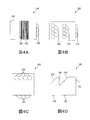
- FIG. 4A to 4D are diagrams showing the configuration of the optical receptacle according to the first embodiment.
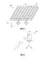
- 5A and 5B are diagrams illustrating the configuration of the light separation unit according to the first embodiment.
- 6A and 6B are diagrams illustrating the configuration of the light separation unit according to the first embodiment.
- 7A and 7B are optical path diagrams in the optical module according to Embodiment 1.
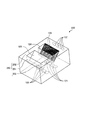
- FIG. FIG. 8 is a perspective view of an optical receptacle according to the second embodiment.
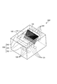
- FIG. 9 is a perspective view of an optical receptacle according to a modification of the second embodiment.
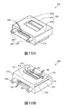
- 10A and 10B are perspective views of an optical receptacle according to the third embodiment.
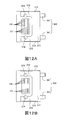
- 11A to 11E are diagrams showing the configuration of the optical receptacle according to the third embodiment.
- 12A and 12B are diagrams showing another arrangement of the first optical surface.
- FIG. 13 is a perspective view showing another form of the light separation unit.
- FIG. 2 is a cross-sectional view of the optical module 100 according to Embodiment 1 of the present invention.
- hatching of the cross section of the optical receptacle 120 is omitted to show the optical path in the optical receptacle 120.
- 2 represents the optical axis of light, and the broken line represents the outer diameter of light.
- the optical module 100 includes a substrate mounting type photoelectric conversion device 110 including a photoelectric conversion element (light emitting element 112 and / or light receiving element 113), and an optical receptacle 120.
- the optical module 100 is used in a state where the optical transmission body 140 is connected to the optical receptacle 120 via a ferrule.
- the type of the optical transmission body 140 is not particularly limited, and includes an optical fiber, an optical waveguide, and the like.
- the optical transmission body 140 is an optical fiber.
- the optical fiber may be a single mode method or a multimode method.
- the number of the optical transmission bodies 140 is not particularly limited. In the present embodiment, four optical fibers are arranged in a line at regular intervals.
- the optical transmission bodies 140 may be arranged in two or more rows.
- the photoelectric conversion device 110 includes a substrate 111, a light emitting element 112 and / or a light receiving element 113, and a detection element 114.
- a light emitting element 112 is used as a photoelectric conversion element.
- a light receiving element 113 is used as a photoelectric conversion element.
- a light emitting element 112 and a light receiving element 113 are used as photoelectric conversion elements.
- a transmission / reception optical module 100 will be described.
- the substrate 111 is, for example, a glass composite substrate, a glass epoxy substrate, a flexible sill substrate, or the like.
- a light emitting element 112 On the substrate 111, a light emitting element 112, a light receiving element 113, and a detecting element 114 are arranged.
- the light emitting element 112 is disposed on the substrate 111, and emits laser light in a direction perpendicular to the surface of the substrate 111 on which the light emitting element 112 is disposed.
- the number of the light emitting elements 112 is not particularly limited. In the present embodiment, the number of light emitting elements 112 is two. Further, the position of the light emitting element 112 is not particularly limited. In the present embodiment, the two light emitting elements 112 are arranged along the arrangement direction of the optical transmission bodies 140 at regular intervals.
- the light emitting element 112 is, for example, a vertical cavity surface emitting laser (VCSEL).
- VCSEL vertical cavity surface emitting laser
- the optical transmission bodies 140 are arranged in two or more rows, the light emitting elements 112 may be arranged in the same number of rows.
- the light receiving element 113 is disposed on the substrate 111 and receives the received light Lr that is at least a part of the light L2 emitted from the optical transmission body 140 (see FIG. 7B).
- the number of light receiving elements 113 is not particularly limited. In the present embodiment, the number of light receiving elements 113 is two. Further, the position of the light receiving element 113 is not particularly limited. In the present embodiment, the two light receiving elements 113 are arranged in a line along the arrangement direction of the optical transmission bodies 140 at regular intervals. Specifically, the two light emitting elements 112 are arranged so as to be positioned on the same straight line.
- the light receiving element 113 is, for example, a photodiode (PD). When the optical transmission bodies 140 are arranged in two or more rows, the light receiving elements 113 may be arranged in the same number of rows.
- PD photodiode
- the detection element 114 is disposed on the substrate 111, and receives monitor light Lm for monitoring the output (for example, intensity and light quantity) of the light L1 emitted from the light emitting element 112.
- the detection element 114 is, for example, a photodiode (PD).
- the detection element 114 is disposed at a position farther from the optical transmission body 140 than the light emitting element 112 and the light receiving element 113. In the present embodiment, when the optical module 100 is viewed in plan, the detection element 114 is disposed on the opposite side of the optical transmission body 140 with the light emitting element 112 and the light receiving element 113 interposed therebetween.
- the number of detection elements 114 is not particularly limited. In the present embodiment, the number of detection elements 114 is two.
- the two detection elements 114 are arranged in a line at regular intervals corresponding to the two light emitting elements 112.
- the detection elements 114 may be arranged in the same number of rows. Further, from the viewpoint of preventing the reflected light from the detection element 114 from returning into the optical receptacle 120, the optical axis of the light incident on the detection element 114 may be inclined with respect to the detection surface 117 of the detection element 114. Good.
- the optical receptacle 120 is disposed on the substrate 111.
- the optical receptacle 120 is optically coupled to the light emitting surfaces 115 of the plurality of light emitting elements 112 and the end surfaces 141 of the plurality of light transmitters 140 in a state of being disposed between the photoelectric conversion device 110 and the light transmitter 140.
- the detection surfaces 117 of the plurality of detection elements 114 and the end surfaces 141 of the plurality of optical transmission bodies 140 are optically coupled to each other.
- the configuration of the optical receptacle 120 will be described in detail.
- FIGS. 3 to 6 are diagrams showing the configuration of the optical receptacle 120 according to the first embodiment.
- 3A is a perspective view of the optical receptacle 120 as viewed from above
- FIG. 3B is a perspective view as viewed from below.
- 4A is a plan view of the optical receptacle 120
- FIG. 4B is a bottom view
- FIG. 4C is a front view
- FIG. 4D is a side view.
- FIG. 5A is a perspective view of the light separating unit 123
- FIG. 5B is a diagram illustrating a positional relationship of surfaces constituting the light separating unit 123.
- FIG. 6A is a partially enlarged cross-sectional view of a portion indicated by a broken line in FIG. 4D.
- FIG. 6B is a diagram for explaining a light amount ratio between the signal light Ls and the monitor light Lm.
- the optical receptacle 120 is a substantially rectangular parallelepiped member.
- the optical receptacle 120 has translucency, and emits the light L1 emitted from the light emitting surface 115 of the light emitting element 112 toward the end surface 141 of the light transmission body 140, while receiving light emitted from the light transmission body 140. Lr is emitted toward the light receiving surface 116 of the light receiving element 113.
- the optical receptacle 120 includes a plurality of first optical surfaces 121, a plurality of second optical surfaces 122, a light separation unit 123, a transmission surface 124, a reflection surface 125, and a plurality of third optical surfaces 126.
- the optical receptacle 120 is formed using a material that is transparent to light having a wavelength used for optical communication. Examples of such materials include transparent resins such as polyetherimide (PEI) and cyclic olefin resins.
- PEI polyetherimide
- cyclic olefin resins
- the first optical surface 121 is an optical surface that causes the light L1 emitted from the light emitting element 112 to enter the inside of the optical receptacle 120 while being refracted.
- the first optical surface 121 is also an optical surface that emits the received light Lr from the optical transmission body 140 that has traveled inside the optical receptacle 120 toward the light receiving element 113 while refracting it.
- the shape of the first optical surface 121 is a convex lens surface that is convex toward the light emitting element 112 (light receiving element 113).
- the first optical surface 121 converts the light L1 emitted from the light emitting element 112 into collimated light.
- the first optical surface 121 converges the collimated light (received light Lr) that has traveled inside the optical receptacle 120.
- the plurality of (four) first optical surfaces 121 are light beams so that the bottom surface of the optical receptacle 120 faces the light emitting surface 115 of the light emitting element 112 and the light receiving surface 116 of the light receiving element 113, respectively.
- the transmitters 140 are arranged in a line along the arrangement direction of the transmitters 140. Further, the planar view shape of the first optical surface 121 is a circle.
- the central axis of the first optical surface 121 is preferably perpendicular to the light emitting surface 115 of the light emitting element 112 and the light receiving surface 116 of the light receiving element 113.
- the central axis of the first optical surface 121 is preferably coincident with the optical axis of the light L1 emitted from the light emitting element 112 (received light Lr incident on the light receiving element 113).
- the light incident on the first optical surface 121 travels toward the light separation unit 123. Further, the received light Lr emitted from the first optical surface 121 travels toward the light receiving element 113.
- the first optical surfaces 121 are also arranged in the same number of rows.
- the two first optical surfaces 121 on the upper side in the drawing are used as the first optical surfaces 121 on the transmission side, and the lower ones Two first optical surfaces 121 are used as the first optical surfaces 121 on the receiving side. That is, the light L1 from the light emitting element 112 is incident on the two first transmission-side first optical surfaces 121 shown in the figure, and the inside of the optical receptacle 120 passes through the two reception-side first optical surfaces 121 shown in the figure. The traveling received light Lr is emitted.
- the four first optical surfaces 121 are equally divided, and one region functions as the transmitting side with the vertical surface with respect to the substrate 111 as the center, and the other region. Functions as a receiver.
- the light separation unit 123 is disposed on the optical path between the first optical surface 121 and the second optical surface 122, and the signal light Ls that is incident on the first optical surface 121 toward the end surface 141 side of the optical transmission body 140.
- the signal light Ls is separated into monitor light Lm traveling toward the detection element 114 so as to travel in a direction substantially opposite to the traveling direction of the signal light Ls.
- the light separation unit 123 causes at least a part of the light incident on the second optical surface 122 to advance toward the light receiving element 113 as the received light Lr.
- the light separation unit 123 includes a plurality of separation units 131.
- the number of separation units 131 is not particularly limited.
- the separation unit 131 includes a first divided reflection surface 132, a second divided reflection surface 133, and a divided transmission surface 134, respectively. That is, the light separation unit 123 includes a plurality of first divided reflection surfaces 132, a plurality of second division reflection surfaces 133, and a plurality of divided transmission surfaces 134.
- the inclination direction of the first divided reflection surface 132 is referred to as a first direction D1.
- the first divided reflection surface 132, the second divided reflection surface 133, and the divided transmission surface 134 are each divided in the first direction D1.
- the first divided reflection surface 132, the second divided reflection surface 133, and the divided transmission surface 134 are arranged in the first direction D1.
- the first split reflection surface 132 is an inclined surface with respect to the optical axis of the light L1 incident on the first optical surface 121.
- the first split reflection surface 132 is also an inclined surface with respect to the optical axis of the light L2 incident on the second optical surface 122.
- the first split reflection surface 132 is inclined so as to be away from the second optical surface 122 (the optical transmission body 140) as it goes from the top surface to the bottom surface of the optical receptacle 120.
- the first split reflecting surface 132 internally reflects a part of the light incident on the first optical surface 121 toward the second optical surface 122 as signal light Ls.
- the first split reflection surface 132 internally reflects part of the light incident on the second optical surface 122 toward the first optical surface 121 as received light Lr.
- the inclination angle of the first split reflection surface 132 is 45 ° with respect to the optical axis of the light L 1 incident on the first optical surface 121 and the optical axis of the light L 2 incident on the second optical surface 122.
- segmentation reflective surface 132 is divided
- segmentation reflective surface 132 is arrange
- the second split reflection surface 133 is an inclined surface with respect to the optical axis of the light L1 incident on the first optical surface 121.
- the second divided reflection surface 133 is inclined in a second direction D2 that is different from the first direction D1 that is the inclination direction of the first divided reflection surface 132.
- the second split reflection surface 133 is inclined so as to approach the second optical surface 122 (the optical transmission body 140) as it goes from the top surface to the bottom surface of the optical receptacle 120.
- the second divided reflection surface 133 reflects a part of the light incident on the second optical surface 122 toward the divided transmission surface 134 as monitor light Lm.
- the inclination angle of the second split reflection surface 133 is 45 ° with respect to the optical axis of the light L1 incident on the first optical surface 121.
- the second divided reflection surface 133 is divided in the first direction D1, and is arranged at a predetermined interval.
- the divided transmission surface 134 is a plane parallel to the optical axis of the light L1 incident on the first optical surface 121.
- the divided transmission surface 134 emits (transmits) the monitor light Lm incident on the first optical surface 121 and reflected by the second divided reflection surface 133.
- the divided transmission surface 134 is also divided in the first direction D1 and arranged at a predetermined interval.
- the first divided reflection surface 132, the second divided reflection surface 133, and the divided transmission surface 134 are in this order in the first direction (from the top surface to the bottom surface).
- Direction D1.
- a ridge line 135 is formed between the second divided reflection surface 133 and the divided transmission surface 134.
- the plurality of ridge lines 135 adjacent in the first direction D1 are arranged in parallel to each other.
- the smaller angle is 45 °.
- the angle formed by the first divided reflection surface 132 and the second divided reflection surface 133 is 90 °.
- the smaller angle among the angles formed by the divided transmission surface 134 and the divided transmission surface 134 (of the adjacent separation unit 131) is 135 °.
- the plurality of separation units 131 are arranged in the first direction D1.
- a part of the light L1 incident on the first optical surface 121 is incident on the first split reflection surface 132 at an incident angle larger than the critical angle.
- the first split reflection surface 132 internally reflects a part of the light L1 incident on the first optical surface 121 toward the second optical surface 122 to generate the signal light Ls.
- a part of the light incident on the second optical surface 122 is also incident on the first split reflection surface 132 at an incident angle larger than the critical angle.
- the first split reflection surface 132 internally reflects a part of the light L2 incident on the second optical surface 122 toward the first optical surface 121 to generate reception light Lr.
- the second split reflection surface 133 a part of the light L1 incident on the first optical surface 121 is internally incident at an incident angle larger than the critical angle.
- the second split reflecting surface 133 internally reflects a part of the light L1 incident on the first optical surface 121 toward the third optical surface 126 side, and generates monitor light Lm.
- the divided transmission surface 134 transmits the monitor light Lm incident on the first optical surface 121 and reflected by the second divided reflection surface 133.
- the light quantity ratio between the signal light Ls and the monitor light Lm is to obtain the monitor light Lm that can monitor the intensity and the light quantity of the light L1 emitted from the light emitting element 112 while obtaining the signal light Ls having a desired light quantity. If possible, it is not particularly limited. As shown in FIG. 6B, the light quantity ratio between the signal light Ls and the monitor light Lm is such that the area S1 of the first divided reflecting surface 132 and the area of the second divided reflecting surface 133 when viewed from the first optical surface 121. It is almost the same as the area ratio with S2.
- signal light Ls: monitor light Lm 5: 5.
- the light quantity ratio between the signal light Ls and the monitor light Lm changes the area ratio between the area S1 of the first divided reflecting surface 132 and the area S2 of the second divided reflecting surface 133 when viewed from the first optical surface 121. Can be adjusted.
- the amount of the received light Lr toward the light receiving surface 116 of the light receiving element 113 is not particularly limited as long as a desired amount of light can be obtained. As shown in FIG.
- the amount of the received light Lr toward the light receiving surface 116 of the light receiving element 113 depends on the ratio of the area S3 of the first divided reflecting surface 132 when viewed from the second optical surface 122.
- the light quantity ratio between the received light Lr reflected by the first divided reflection surface 132 and the light emitted from the divided transmission surface 134 is 5: 5.
- the second optical surface 122 is an optical surface that emits the signal light Ls incident on the first optical surface 121 and reflected by the first divided reflection surface 132 toward the end surface 141 of the optical transmission body 140.
- the second optical surface 122 is also an optical surface that causes the light L2 emitted from the end surface 141 of the optical transmission body 140 to enter the inside of the optical receptacle 120 while being refracted.
- the shape of the second optical surface 122 is a convex lens surface that is convex toward the end surface 141 of the optical transmission body 140.
- the second optical surface 122 converges the light traveling in the optical receptacle 120 toward the end surface 141 of the optical transmission body 140 and converts the light emitted from the end surface 141 of the optical transmission body 140 into collimated light.
- a plurality (four) of the second optical surfaces 122 are arranged in the arrangement direction of the optical transmission body 140 so as to face the end surface 141 of the optical transmission body 140 on the front surface of the optical receptacle 120, respectively. Are arranged in one row.
- the planar view shape of the second optical surface 122 is a circle.
- the central axis of the second optical surface 122 is preferably perpendicular to the end surface 141 of the optical transmission body 140.
- the central axis of the second optical surface 122 is preferably coincident with the optical axis of the light emitted from the optical transmission body 140.
- the second optical surfaces 122 are also arranged in the same number of rows.
- the two second optical surfaces 122 on the left side in the drawing are used as the second optical surfaces 122 on the transmission side, and the right side.
- These two second optical surfaces 122 are used as the second optical surfaces 122 on the receiving side. That is, the reception light Lr that has passed through the inside of the optical receptacle 120 is emitted from the two second optical surfaces 122 on the left side in the figure, and the two optical surfaces 122 on the right side in the figure are transmitted to the optical transmission body. Light L2 emitted from 140 enters.
- the transmission surface 124 is disposed on the top surface side of the optical receptacle 120, and makes the monitor light Lm emitted from the divided transmission surface 134 of the light separation unit 123 out of the optical receptacle 120 enter the optical receptacle 120 again.
- the transmission surface 124 is a surface perpendicular to the optical axis of the monitor light Lm emitted from the divided transmission surface 134 (a parallel surface parallel to the optical axis of the light L1 emitted from the light emitting element 112).
- the transmission surface 124 may be an inclined surface with respect to the optical axis of the monitor light Lm emitted from the divided transmission surface 134. In this case, the transmission surface 124 is inclined so as to approach the reflection surface 125 from the bottom surface of the optical receptacle 120 toward the top surface.
- the inclination angle of the transmission surface 124 that is an inclined surface is not particularly limited, but is preferably an inclination angle corresponding to a punch taper for mold release in injection molding.
- the reflection surface 125 is disposed on the top surface side of the optical receptacle 120 and reflects the monitor light Lm incident on the transmission surface 124 toward the third optical surface 126 side.
- the reflecting surface 125 is inclined so as to move away from the second optical surface 122 (the optical transmission body 140) as it goes from the top surface to the bottom surface of the optical receptacle 120.
- the inclination angle of the reflecting surface 125 is 45 ° with respect to the optical axis of the light L1 incident on the first optical surface 121 and the optical axis of the light L2 incident on the second optical surface 122.
- the third optical surface 126 is disposed on the bottom surface side of the optical receptacle 120, is separated by the light separation unit 123, passes through the transmission surface 124, and converges the monitor light Lm reflected by the reflection surface 125 to detect the detection element.
- the light is emitted toward 114.
- the third optical surface 126 is a convex lens surface that is convex toward the detection element 114.
- the central axis of the third optical surface 126 is preferably inclined with respect to the detection surface 117 (substrate 111) of the detection element 114.
- the manufacturing method of the optical receptacle 120 is not particularly limited.
- the optical receptacle 120 is manufactured by injection molding, for example.
- a die piece having a surface complementary to the light separating portion 123 and the transmission surface 124 is used.
- a resin or the like used as a material is formed in a region formed by the surface corresponding to the second divided reflection surface 133 and the surface corresponding to the divided transmission surface 134 of the cavity (portion that becomes the optical receptacle 120) in the mold. It is assumed that is difficult to enter.
- the ridgeline 135 (the region formed by the second divided reflection surface 133 and the divided transmission surface 134) of the separation unit 131 in the optical receptacle 120 that is a molded product may not be appropriately formed.
- the light reaching the top of the separation unit 131 is light that becomes the monitor light Lm that does not require high accuracy, and thus the top of the separation unit 131 is appropriately shaped. Even if not, it will not be a big problem.
- the plurality of first divided reflecting surfaces 132 are arranged so as to be positioned on the same plane, and can be surely formed appropriately. Therefore, the plurality of first divided reflecting surfaces 132 that generate the light that becomes the signal light Ls that greatly affects the communication accuracy can be formed with high accuracy.
- FIG. 7 is a diagram showing an optical path in the optical module.
- FIG. 7A is an optical path diagram on the transmitting side
- FIG. 7B is an optical path diagram on the receiving side.
- FIGS. 7A and 7B only the optical axis is indicated by a one-dot chain line.
- the light L1 emitted from the light emitting element 112 enters the optical receptacle 120 through the first optical surface 121.
- a part of the light incident on the optical receptacle 120 is internally reflected by the first split reflection surface 132 toward the second optical surface 122 to become signal light Ls.
- the signal light Ls reflected by the first split reflection surface 132 is emitted from the second optical surface 122 and reaches the end surface 141 of the optical transmission body 140.
- the light L1 emitted from the light emitting element 112 passes only through the first optical surface 121 and the second optical surface 122 and reaches the optical transmission body 140.
- all the optical paths between the first optical surface 121 and the second optical surface 122 are located inside the optical receptacle 120.
- another part of the light incident on the optical receptacle 120 is reflected by the second divided reflection surface 133 toward the reflection surface 125 to become monitor light Lm.
- the monitor light Lm is emitted to the outside of the optical receptacle 120 through the divided transmission surface 134, then enters the inside of the optical receptacle 120 again through the transmission surface 124, and is reflected by the reflection surface 125.
- the monitor light Lm reflected by the reflection surface 125 is emitted from the third optical surface 126 and reaches the detection element 114.
- the light L2 emitted from the optical transmission body 140 enters the optical receptacle 120 through the second optical surface 122.
- Part of the light incident on the optical receptacle 120 is internally reflected toward the first optical surface 121 by the first split reflection surface 132 and becomes received light Lr.
- the reception light Lr reflected by the first split reflection surface 132 is emitted from the first optical surface 121 and reaches the light receiving surface 116 of the light receiving element 113.
- the light emitted from the optical transmission body 140 passes only through the second optical surface 122 and the first optical surface 121 and reaches the light receiving element 113.
- the entire optical path between the second optical surface 122 and the first optical surface 121 is located inside the optical receptacle 120. Note that another part of the light incident on the optical receptacle 120 at the second optical surface 122 is emitted to the outside of the optical receptacle 120 at the divided transmission surface 134 and then reenters the optical receptacle 120 at the transmission surface 124. Then, the light is reflected by the reflection surface 125.
- the light utilization efficiency in the optical receptacle 120 according to the present embodiment was simulated.
- the material of the optical receptacle 120 was polyetherimide (PEI), and the pitch of the separation units 131 was 0.0275 mm. Specifically, when 1 W of light was emitted from the light emitting element 112, the utilization efficiency of light reaching the optical transmission body 140 and the detection element 114 was obtained. In this simulation, the area of the first divided reflection surface 132 and the area of the second division reflection surface 133 when viewed from the light emitting element 112 side are the same. For comparison, the light use efficiency in the optical receptacle 10 (see FIG. 1) described in Patent Document 1 was also obtained.
- the optical receptacle 10 described in Patent Document 1 in the optical path from the light emitting element 112 to the optical transmission body 140, compared with the optical receptacle 120 according to the present embodiment, two interfaces (the light separation unit 34 and the incident surface) are further provided. 37) is transmitted.
- the amount of light is lost by about 5.8% ( ⁇ 0.26 dB) every time it passes through one interface. Therefore, the optical receptacle 10 described in Patent Document 1 loses ⁇ 0.52 dB ( ⁇ 0.26 dB ⁇ 2) of light from the optical receptacle 120 according to the present embodiment. That is, it can be seen that the light use efficiency of the optical receptacle 120 according to the present embodiment is 10.16% (0.52 dB) higher than the optical receptacle 10 described in Patent Document 1.
- the optical receptacle 120 As described above, in the optical receptacle 120 according to the first embodiment, the light L1 emitted from the light emitting element 112 (the light receiving element 113) is transmitted through the first optical surface 121 and the second optical surface 122 only. Since the light reaches the body 140, reflected light and stray light reflected at the interface can be reduced. Therefore, in the optical receptacle 120 according to the present embodiment, the light utilization efficiency can be improved as compared with the conventional optical receptacle (the optical receptacle 10 described in Patent Document 1). Further, the optical module 100 according to Embodiment 1 can be easily downsized because the optical path length between the first optical surface 121 and the second optical surface 122 can be easily shortened.
- the optical receptacle 120 according to the present embodiment is Can be manufactured at low cost.
- the optical module according to the second embodiment is different from the optical module 100 according to the first embodiment only in the configuration of the optical receptacle. Therefore, the same components as those in the first embodiment are denoted by the same reference numerals and description thereof is omitted.
- the optical module according to Embodiment 2 includes a photoelectric conversion device 110 and an optical receptacle 220.
- the optical module is used in a state where the optical transmission body 140 is connected to the optical receptacle 220 via a ferrule.
- four optical fibers are arranged in a line at regular intervals.
- FIG. 8 is a perspective view of the optical receptacle 220 according to the second embodiment.
- the optical receptacle 220 according to the second embodiment includes a plurality of first optical surfaces 121, a plurality of second optical surfaces 122, a light separation unit 123, a transmission surface 124, a reflection surface 125, and a plurality of A third optical surface 126 and a frame body 250 are provided.
- the frame body 250 is disposed around the light separating portion 123 and the reflecting surface 125.
- the frame 250 has a back wall 251 located on the back side of the optical receptacle 220 and a side wall 252 located on the side.
- the top surface of the frame body 250 is disposed so as to be flush with the top surface between the light separating portion 123 and the reflecting surface 125. Thereby, the light separation part 123 and the reflective surface 125 can be protected appropriately.
- FIG. 9 is a perspective view of an optical receptacle 220 'according to a modification of the second embodiment. As shown in FIG. 9, the optical receptacle 220 ′ may not have a top surface between the transmission surface 124 and the reflection surface 125.
- the optical receptacles 220 and 220 ′ according to the second embodiment appropriately provide the light separation unit 123, the transmission surface 124, and the reflection surface 125 from foreign matters. Can be protected. In addition, generation of stray light can be suppressed.
- the optical module according to the third embodiment is different from the optical module according to the second embodiment only in the configuration of the optical receptacle. Therefore, the same components as those in the second embodiment are denoted by the same reference numerals and description thereof is omitted.
- the optical module according to Embodiment 3 includes a photoelectric conversion device 110 and an optical receptacle 320.
- FIG. 10A is a perspective view of the optical receptacle 320 according to Embodiment 3 as seen from above, and FIG. 10B is a perspective view as seen from below.
- 11A is a plan view of optical receptacle 320 according to Embodiment 3
- FIG. 11B is a cross-sectional view
- FIG. 11C is a front view
- FIG. 11D is a rear view
- FIG. It is a bottom view.
- the hatching to the cross section of the optical receptacle 320 of FIG. 11B is abbreviate
- the optical receptacle 320 includes a plurality of first optical surfaces 121, a plurality of second optical surfaces 122, a light separation unit 123, and a transmission surface 124. , A reflection surface 125, a plurality of third optical surfaces 126, a frame body 250, a ferrule attachment portion 360, and a substrate attachment portion 370.
- the number of first optical surfaces 121, second optical surfaces 122, and third optical surfaces 126 is twelve.
- the six first optical surfaces 121 on the upper side in the drawing are used as the first optical surfaces 121 on the transmission side, and the lower ones Six first optical surfaces 121 are used as the first optical surfaces 121 on the receiving side.
- the twelve first optical surfaces 121 are equally divided, and one region functions as the transmitting side with the vertical surface with respect to the substrate 111 as the center, and the other region. Functions as a receiver.
- the ferrule attachment part 360 is a part for attaching and detaching the ferrule that fixes the optical transmission body 140.
- Ferrule mounting portion 360 is disposed in front of optical receptacle 320.
- the configuration of the ferrule attachment portion 360 is not particularly limited as long as the ferrule can be attached and detached.
- ferrule mounting portion 360 has a pair of protrusions 361 that are arranged so as to sandwich all of second optical surface 122 in the long side direction.
- the shape and number of the protrusions 361 are not particularly limited as long as the ferrule can be fixed to the optical receptacle 320. That is, the shape of the protrusion 361 may be a shape complementary to the concave portion of the ferrule.
- the substrate attachment unit 370 fixes the optical receptacle 320 at a predetermined position with respect to the substrate 111. Specifically, the substrate attachment portion 370 fixes the optical receptacle 320 at a predetermined position with respect to the substrate 111, thereby causing the first optical to the light emitting surface 115 of the light emitting element 112 and the light receiving surface 116 of the light receiving element 113. While positioning the surface 121, the third optical surface 126 is positioned with respect to the detection surface 117 of the detection element 114.
- the configuration of the substrate attachment portion 370 is not particularly limited as long as the above-described function can be exhibited. In the present embodiment, substrate mounting portion 370 is a convex portion disposed on the bottom surface of optical receptacle 320.
- the substrate attachment portion 370 is disposed on the bottom surface of the optical receptacle 320 except for the first optical surface 121, the third optical surface 126, and the region on the back side of the optical receptacle 320.
- the substrate attachment part 370 has a front part 371 located on the front side of the optical receptacle 320 and a side part 372 located on the side of the optical receptacle 320.
- An adhesive accommodating groove 373 and a fitting recess 374 are disposed on the side surface portion 372.
- the adhesive accommodating groove 373 is a notch groove disposed on the side surface side of the optical receptacle 320 (outside the side surface portion 372).
- the fitting recess 374 is disposed on the first optical surface 121 and the third optical surface 126 side.
- the fitting recess 374 is formed to be complementary to the fitting protrusion of the substrate 111 (not shown).
- the optical receptacle 320 according to the third embodiment has the same effect as the optical receptacle 220 according to the second embodiment.
- the optical receptacle 320 according to the third embodiment has the fitting recess 374 formed complementarily to the fitting projection of the substrate 111, it can be easily positioned with respect to the substrate 111.
- the third optical surface 126 may be arranged corresponding to the number of light emitting elements 112 that emit the signal light Ls. Further, as shown in FIG. 12B, the area on the transmission side and the area on the reception side may be arranged apart from each other.
- the separation units 131 of the light separation unit 123 are alternately arranged in a third direction D3 orthogonal to the first direction D1 and the second direction D2 so as to form a matrix. It may be.
- a reflective film such as a thin film of a metal having a high light reflectance (for example, Al, Ag, Au, etc.) may be formed on the reflective surface 125, the first divided reflective surface 132, and the second divided reflective surface 133. .
- a metal having a high light reflectance for example, Al, Ag, Au, etc.
- the light separation part 123 of this Embodiment has the 1st division
- the transmission / reception optical receptacle 120 has been described. However, a transmission optical receptacle or a reception optical receptacle may be used.
- a transmission optical receptacle or a reception optical receptacle may be used.
- a plurality of light emitting elements 112 and a plurality of detection elements 114 are arranged.
- the plurality of first optical surfaces 121 allow the light L1 emitted from the plurality of light emitting elements 112 to enter.
- the plurality of second optical surfaces 122 respectively emit the signal light Ls reflected by the first split reflection surface 132 toward the end surfaces 141 of the plurality of optical transmission bodies 140.
- the plurality of third optical surfaces 126 respectively emit the monitor light Lm reflected by the reflection surface 125 toward the detection surface 117 of the detection element 114.
- a plurality of light receiving elements 113 are arranged.
- the plurality of second optical surfaces 122 allow the light L2 emitted from the plurality of optical transmission bodies 140 to enter.
- the plurality of first optical surfaces 121 emit the received light Lr reflected by the first divisional reflecting surface 132 toward the light receiving surface 116 of the light receiving element 113.
- the number of the light emitting element 112, the light receiving element 113, the detecting element 114, the first optical surface 121, the second optical surface 122, the third optical surface 126, and the optical transmission body 140 is four. One by one.
- the number of the light emitting elements 112, the light receiving elements 113, the detecting elements 114, the first optical surfaces 121, the second optical surfaces 122, the third optical surfaces 126, and the optical transmission bodies 140 is twelve. is there.
- optical receptacle and the optical module according to the present invention are useful for optical communication using, for example, an optical transmission body.
- Optical module 20 Photoelectric conversion device 21 Light emitting element 22 Optical transmission body 23 End surface 24 Detection element 30 Optical receptacle 31 1st optical surface 32 2nd optical surface 33 Reflecting surface 34 Light separation part 35 3rd optical surface 36 Concave part 37 Incidence surface 100 Optical module 110 Photoelectric conversion device 111 Substrate 112 Light emitting element 113 Light receiving element 114 Detection element 115 Light emitting surface 116 Light receiving surface 117 Detection surface 120, 220, 220 ′, 320 Optical receptacle 121 First optical surface 122 Second optical surface 123 Light separation unit 124 Transmission surface 125 Reflection surface 126 Third optical surface 131 Separation unit 132 First divided reflection surface 133 Second divided reflection surface 134 Divided transmission surface 135 Ridge line 140 Optical transmission body 141 End face 250 Frame body 251 Back wall 252 Side wall 360 Ferrule attachment Part 361 Protrusion 3 70 Substrate mounting portion 3
Landscapes
- Physics & Mathematics (AREA)
- General Physics & Mathematics (AREA)
- Optics & Photonics (AREA)
- Condensed Matter Physics & Semiconductors (AREA)
- Electromagnetism (AREA)
- Optical Couplings Of Light Guides (AREA)
- Optical Elements Other Than Lenses (AREA)
- Semiconductor Lasers (AREA)
Abstract
本発明の光レセプタクルは、光電変換素子から出射された光を入射させる第1光学面と、第1光学面で入射した光を光伝送体の端面に向けて出射させる第2光学面と、第1光学面および第2光学面の間の光路上に配置され、第1光学面で入射した光を光伝送体の端面側に向かう信号光と信号光の進行方向と略反対方向に進行するように検出素子側に向かうモニター光とに分離させる光分離部と、光分離部で分離されたモニター光を検出素子に向けて出射させる第3光学面と、を有する。第1光学面および第2光学面の間の全光路は、光レセプタクルの内部に位置している。
Description
本発明は、光レセプタクルおよびこれを有する光モジュールに関する。
従来、光ファイバーや光導波路などの光伝送体を用いた光通信には、面発光レーザー(例えば、VCSEL:Vertical Cavity Surface Emitting Laser)などの発光素子を備えた光モジュールが使用されている。光モジュールは、発光素子から出射された通信情報を含む光を、光伝送体の端面に入射させる光レセプタクルを有する。
また、光モジュールには、温度変化に対する発光素子の出力特性の安定化や光出力の調整を目的として、発光素子から出射された光の強度や光量を監視(モニター)するための検出素子を有するものがある。
たとえば、特許文献1には、発光素子および検出素子が配置された光電変換装置と、発光素子と光伝送体の端面とを光学的に接続させる光レセプタクルとを有する光モジュールが記載されている。
図1は、特許文献1に記載の光モジュール10の構成を模式的に示す断面図である。図1に示されるように、特許文献1に記載の光モジュール10は、光電変換装置20と、樹脂製の光レセプタクル30とを有する。光レセプタクル30は、発光素子21から出射された光を入射させる第1光学面31と、内部を通る光を光伝送体22の端面23に集光するように出射する第2光学面32と、第1光学面31で入射した光を光伝送体22側に反射する反射面33と、反射面33で反射した光を検出素子24側に向かうモニター光Lmおよび光伝送体22側に向かう信号光Lsに分離する光分離部34と、モニター光Lmを検出素子24に向けて出射させる第3光学面35とを有する。また、光分離部34は、光レセプタクル30に形成された凹部36の内面の一部として形成されている。
特許文献1に記載の光モジュール10では、発光素子21から出射され、第1光学面31で入射した光は、光分離部34に向けて反射面33で反射する。反射面33で反射した光は、光分離部34によって信号光Lsおよびモニター光Lmに分離される。光分離部34で分離されたモニター光Lmは、検出素子24の受光面に向けて第3光学面35から出射される。一方、光分離部34で分離された信号光Lsは、光分離部34を透過して光レセプタクル30の外部に出射される。そして、凹部36の内面の他の一部である入射面37から再び光レセプタクル30に入射する。入射面37で入射した信号光Lsは、光伝送体22の端面23に向けて第2光学面32から出射される。
しかしながら、特許文献1に記載の光モジュール10では、発光素子21から出射された光は、光レセプタクル30(樹脂)と空気との間の複数の界面を透過して光伝送体22に到達する。このとき、発光素子21から出射された光の一部は、界面において反射されてしまう。また、光レセプタクル30内を進行する光は、光レセプタクル30を構成する樹脂によって少しずつ吸収されてしまうため、光レセプタクル30内の信号光Lsの光路が長いと、信号光Lsの損失が問題となる。よって、特許文献1に係る光モジュール10には、発光素子21から出射された光の利用効率を向上させる余地がある。また、特許文献1に係る光モジュール10には、小型化する余地もある。
そこで、本発明の目的は、小型化しつつ、発光素子から出射された光の利用効率を向上させることができる光レセプタクルを提供することである。また、本発明の目的は、この光レセプタクルを有する光モジュールを提供することでもある。
本発明に係る光レセプタクルは、1または2以上の光伝送体と、1または2以上の光電変換素子、および前記光電変換素子よりも前記光伝送体から離れた位置に配置され、前記光電変換素子から出射された光を監視するための1または2以上の検出素子を含む光電変換装置との間に配置され、前記光電変換素子と前記光伝送体の端面とを光学的に結合するための光レセプタクルであって、前記光電変換素子から出射された光を入射させるか、前記光伝送体の端面から出射され、前記光レセプタクルの内部を通る光を前記光電変換素子に向けて出射させる、1または2以上の第1光学面と、前記第1光学面で入射した光を前記光伝送体の端面に向けて出射させるか、前記光伝送体の端面から出射された光を入射させる、1または2以上の第2光学面と、前記第1光学面および前記第2光学面の間の光路上に配置され、前記第1光学面で入射した光を前記光伝送体の端面側に向かう信号光と前記信号光の進行方向と略反対方向に進行するように前記検出素子側に向かうモニター光とに分離させるか、前記第2光学面で入射した光の少なくとも一部を受信光として前記光電変換素子側に出射させる光分離部と、前記光分離部で分離された前記モニター光を前記検出素子に向けて出射させる、1または2以上の第3光学面と、を有し、前記第1光学面および前記第2光学面の間の全光路は、前記光レセプタクルの内部に位置している。
本発明に係る光モジュールは、基板と、前記基板上に配置された1または2以上の光電変換素子と、前記基板上に配置され、前記光電変換素子から出射された光を監視するための1または2以上の検出素子とを有する光電変換装置と、本発明に係る光レセプタクルと、を有し、前記検出素子は、前記基板上において前記光電変換素子よりも前記光伝送体から離れる位置に配置されている。
本発明によれば、小型、かつ発光素子から出射された光の利用効率に優れる光レセプタクルおよび光モジュールを提供することができる。
以下、本発明に係る実施の形態について、図面を参照して詳細に説明する。
[実施の形態1]
(光モジュールの構成)
図2は、本発明の実施の形態1に係る光モジュール100の断面図である。なお、図2では、光レセプタクル120内の光路を示すために光レセプタクル120の断面へのハッチングを省略している。また、図2の一点鎖線は、光の光軸を示しており、破線は、光の外径を示している。
(光モジュールの構成)
図2は、本発明の実施の形態1に係る光モジュール100の断面図である。なお、図2では、光レセプタクル120内の光路を示すために光レセプタクル120の断面へのハッチングを省略している。また、図2の一点鎖線は、光の光軸を示しており、破線は、光の外径を示している。
図2に示されるように、光モジュール100は、光電変換素子(発光素子112および/または受光素子113)を含む基板実装型の光電変換装置110と、光レセプタクル120とを有する。光モジュール100は、光レセプタクル120に光伝送体140がフェルールを介して接続された状態で使用される。
光伝送体140の種類は、特に限定されず、光ファイバー、光導波路などが含まれる。本実施の形態では、光伝送体140は、光ファイバーである。光ファイバーは、シングルモード方式であってもよいし、マルチモード方式であってもよい。光伝送体140の数は、特に限定されない。本実施の形態では、4本の光ファイバーが一定間隔で1列に配列されている。なお、光伝送体140は、2列以上に配列されていてもよい。
光電変換装置110は、基板111と、発光素子112および/または受光素子113と、検出素子114とを有する。送信用の光モジュール100では、光電変換素子として発光素子112が使用される。また、受信用の光モジュール100では、光電変換素子として受光素子113が使用される。さらに、送受信用の光モジュール100では、光電変換素子として発光素子112および受光素子113が使用される。本実施の形態では、送受信用の光モジュール100について説明する。
基板111は、例えば、ガラスコンポジット基板やガラスエポキシ基板、フレキブシル基板などである。基板111上には、発光素子112、受光素子113および検出素子114が配置されている。
発光素子112は、基板111上に配置されており、発光素子112が配置された基板111の表面に対して垂直方向にレーザー光を出射する。発光素子112の数は、特に限定されない。本実施の形態では、発光素子112の数は、2個である。また、発光素子112の位置も特に限定されない。本実施の形態では、2個の発光素子112は、一定間隔で光伝送体140の配列方向に沿って配列されている。発光素子112は、例えば垂直共振器面発光レーザー(VCSEL)である。なお、光伝送体140が2列以上に配列されている場合は、発光素子112も同じ列数で配列されてもよい。
受光素子113は、基板111上に配置されており、光伝送体140から出射された光L2のうち少なくとも一部である受信光Lrを受光する(図7B参照)。受光素子113の数は、特に限定されない。本実施の形態では、受光素子113の数は、2個である。また、受光素子113の位置も特に限定されない。本実施の形態では、2個の受光素子113は、一定間隔で光伝送体140の配列方向に沿って1列に配列されている。具体的には、2個の発光素子112と同一直線上に位置するように配列されている。受光素子113は、例えば、フォトダイオード(PD)である。なお、光伝送体140が2列以上に配列されている場合は、受光素子113も同じ列数で配列されてもよい。
検出素子114は、基板111上に配置されており、発光素子112から出射された光L1の出力(例えば、強度や光量)を監視するためのモニター光Lmを受光する。検出素子114は、例えばフォトダイオード(PD)である。検出素子114は、発光素子112および受光素子113よりも光伝送体140から離れた位置に配置されている。本実施の形態では、光モジュール100を平面視したときに、検出素子114は、発光素子112および受光素子113を挟んで光伝送体140と反対側に配置されている。検出素子114の数は、特に限定されない。本実施の形態では、検出素子114の数は、2個である。2個の検出素子114は、2個の発光素子112に対応して一定間隔で1列に配列されている。なお、光伝送体140が2列以上に配列されている場合は、検出素子114も同じ列数で配列されてもよい。また、検出素子114からの反射光が光レセプタクル120内に戻ることを防止する観点から、検出素子114へ入射する光の光軸は、検出素子114の検出面117に対して傾斜していてもよい。
光レセプタクル120は、基板111上に配置されている。光レセプタクル120は、光電変換装置110と光伝送体140との間に配置された状態で、複数の発光素子112の発光面115と複数の光伝送体140の端面141とをそれぞれ光学的に結合させるとともに、複数の検出素子114の検出面117と複数の光伝送体140の端面141とをそれぞれ光学的に結合させる。以下、光レセプタクル120の構成について詳細に説明する。
(光レセプタクルの構成)
図3~6は、実施の形態1に係る光レセプタクル120の構成を示す図である。図3Aは、光レセプタクル120を上から見た斜視図であり、図3Bは、下から見た斜視図である。図4Aは、光レセプタクル120の平面図であり、図4Bは、底面図であり、図4Cは、正面図であり、図4Dは、側面図である。図5Aは、光分離部123の斜視図であり、図5Bは、光分離部123を構成する面の位置関係を示す図である。図6Aは、図4Dの破線で示される部分の部分拡大断面図である。図6Bは、信号光Lsとモニター光Lmとの光量比を説明するための図である。
図3~6は、実施の形態1に係る光レセプタクル120の構成を示す図である。図3Aは、光レセプタクル120を上から見た斜視図であり、図3Bは、下から見た斜視図である。図4Aは、光レセプタクル120の平面図であり、図4Bは、底面図であり、図4Cは、正面図であり、図4Dは、側面図である。図5Aは、光分離部123の斜視図であり、図5Bは、光分離部123を構成する面の位置関係を示す図である。図6Aは、図4Dの破線で示される部分の部分拡大断面図である。図6Bは、信号光Lsとモニター光Lmとの光量比を説明するための図である。
図2、図3A、Bおよび図4A~Dに示されるように、光レセプタクル120は、略直方体形状の部材である。光レセプタクル120は、透光性を有し、発光素子112の発光面115から出射された光L1を光伝送体140の端面141に向けて出射させる一方、光伝送体140から出射された受信光Lrを受光素子113の受光面116に向けて出射させる。光レセプタクル120は、複数の第1光学面121、複数の第2光学面122、光分離部123、透過面124、反射面125および複数の第3光学面126を有する。光レセプタクル120は、光通信に用いられる波長の光に対して透光性を有する材料を用いて形成される。そのような材料の例には、ポリエーテルイミド(PEI)や環状オレフィン樹脂などの透明な樹脂が含まれる。
第1光学面121は、発光素子112から出射された光L1を屈折させながら光レセプタクル120の内部に入射させる光学面である。また、第1光学面121は、光レセプタクル120の内部を進行してきた光伝送体140からの受信光Lrを屈折させながら受光素子113に向けて出射させる光学面でもある。本実施の形態では、第1光学面121の形状は、発光素子112(受光素子113)に向かって凸状の凸レンズ面である。第1光学面121は、発光素子112から出射された光L1をコリメート光に変換させる。また、第1光学面121は、光レセプタクル120の内部を進行してきたコリメート光(受信光Lr)を収束させる。また、本実施の形態では、複数(4個)の第1光学面121は、光レセプタクル120の底面に、発光素子112の発光面115および受光素子113の受光面116とそれぞれ対向するように光伝送体140の配列方向に沿って1列に配列されている。また、第1光学面121の平面視形状は、円形である。第1光学面121の中心軸は、発光素子112の発光面115および受光素子113の受光面116に対して垂直であることが好ましい。また、第1光学面121の中心軸は、発光素子112から出射された光L1(受光素子113に入射する受信光Lr)の光軸と一致することが好ましい。
第1光学面121で入射した光は、光分離部123に向かって進行する。また、第1光学面121から出射した受信光Lrは、受光素子113に向かって進行する。なお、発光素子112および受光素子113が2列以上に配列されている場合は、第1光学面121も同じ列数で配列される。
本実施の形態では、図4Bに示されるように、4個の第1光学面121のうち、図示上側の2個の第1光学面121を発信側の第1光学面121とし、下側の2個の第1光学面121を受信側の第1光学面121として使用している。すなわち、図示上側2個の発信側の第1光学面121には、発光素子112からの光L1が入射し、図示下側2個の受信側の第1光学面121から光レセプタクル120の内部を進行してきた受信光Lrが出射する。このように、本実施の形態に係る光レセプタクル120では、4個の第1光学面121を等分し、かつ基板111に対する垂直面を中心として一方の領域は発信側として機能し、他方の領域は受信側として機能する。
光分離部123は、第1光学面121および第2光学面122の間の光路上に配置され、第1光学面121で入射した光を光伝送体140の端面141側に向かう信号光Lsと信号光Lsの進行方向と略反対方向に進行するように検出素子114側に向かうモニター光Lmとに分離させる。また、光分離部123は、第2光学面122で入射した光の少なくとも一部を受信光Lrとして受光素子113側に進行させる。
図5に示されるように、光分離部123は、複数の分離ユニット131を有する。分離ユニット131の数は、特に限定されない。分離ユニット131は、第1分割反射面132、第2分割反射面133および分割透過面134をそれぞれ1つずつ含む。すなわち、光分離部123は、複数の第1分割反射面132と、複数の第2分割反射面133と、複数の分割透過面134とを有する。以下の説明では、第1分割反射面132の傾斜方向を第1の方向D1と称する。第1分割反射面132、第2分割反射面133および分割透過面134は、それぞれ第1の方向D1に分割されている。また、第1分割反射面132、第2分割反射面133および分割透過面134は第1の方向D1に配列されている。
第1分割反射面132は、第1光学面121で入射した光L1の光軸に対する傾斜面である。第1分割反射面132は、第2光学面122で入射した光L2の光軸に対する傾斜面でもある。本実施の形態では、第1分割反射面132は、光レセプタクル120の天面から底面に向かうにつれて第2光学面122(光伝送体140)から離れるように傾斜している。第1分割反射面132は、第1光学面121で入射した光の一部を信号光Lsとして第2光学面122側に向けて内部反射させる。また、第1分割反射面132は、第2光学面122で入射した光の一部を受信光Lrとして第1光学面121側に向けて内部反射させる。第1分割反射面132の傾斜角は、第1光学面121で入射した光L1の光軸および第2光学面122で入射した光L2の光軸に対して45°である。第1分割反射面132は、第1の方向D1に分割されており、所定の間隔で配置されている。第1分割反射面132は、第1の方向D1において同一平面上に配置されている。
第2分割反射面133は、第1光学面121で入射した光L1の光軸に対する傾斜面である。第2分割反射面133は、第1分割反射面132の傾斜方向である第1の方向D1と異なる第2の方向D2に傾斜している。具体的には、第2分割反射面133は、光レセプタクル120の天面から底面に向かうにつれて第2光学面122(光伝送体140)に近づくように傾斜している。第2分割反射面133は、第2光学面122で入射した光の一部をモニター光Lmとして分割透過面134側に向けて反射させる。第2分割反射面133の傾斜角は、第1光学面121で入射した光L1の光軸に対して45°である。第2分割反射面133は、第1の方向D1に分割されており、所定の間隔で配置されている。
分割透過面134は、第1光学面121で入射した光L1の光軸に対する平行面である。分割透過面134は、第1光学面121で入射し、第2分割反射面133で反射したモニター光Lmを出射(透過)させる。分割透過面134も、第1の方向D1に分割されており、所定の間隔で配置されている。
図5Bに示されるように、1つの分離ユニット131内において、第1分割反射面132、第2分割反射面133および分割透過面134は、この順番で第1の方向(天面から底面に向かう方向)D1に配列されている。第2分割反射面133および分割透過面134の間には、稜線135が形成される。本実施の形態では、第1の方向D1において隣接する複数の稜線135は、互いに平行に配置されている。第2分割反射面133および分割透過面134のなす角度のうち小さい角度は、45°である。また、第1分割反射面132および第2分割反射面133のなす角度は、90°である。また、分割透過面134および(隣の分離ユニット131の)分割透過面134のなす角度のうち小さい角度は135°である。光分離部123において、複数の分離ユニット131は、第1の方向D1に配列されている。
図6Aに示されるように、第1分割反射面132には、第1光学面121で入射した光L1の一部の光が、臨界角より大きな入射角で内部入射する。第1分割反射面132は、第1光学面121で入射した光L1の一部の光を第2光学面122側に向けて内部反射させて、信号光Lsを生成する。また、特に図示しないが、第1分割反射面132には、第2光学面122で入射した光の一部の光も、臨界角より大きな入射角で内部入射する。第1分割反射面132は、第2光学面122で入射した光の一部の光L2を第1光学面121側に向けて内部反射させて、受信光Lrを生成する。
また、第2分割反射面133は、第1光学面121で入射した光L1の一部の光が、臨界角より大きな入射角で内部入射する。第2分割反射面133は、第1光学面121で入射した光L1の一部の光を第3光学面126側に向けて内部反射させて、モニター光Lmを生成する。
また、分割透過面134は、第1光学面121で入射し、第2分割反射面133で反射したモニター光Lmを透過させる。
信号光Lsとモニター光Lmとの光量比は、所望の光量の信号光Lsを得つつ、発光素子112から出射された光L1の強度や光量を監視することができるモニター光Lmを得ることができれば、特に限定されない。図6Bに示されるように、信号光Lsとモニター光Lmとの光量比は、第1光学面121から見たときの、第1分割反射面132の面積S1と第2分割反射面133の面積S2との面積比とほぼ同じである。信号光Lsとモニター光Lmとの光量比は、信号光Ls:モニター光Lm=5:5~8:2であることが好ましく、信号光Ls:モニター光Lm=7:3であることがさらに好ましい。本実施の形態では、信号光Ls:モニター光Lm=5:5である。信号光Lsとモニター光Lmとの光量比は、第1光学面121から見たときの、第1分割反射面132の面積S1と第2分割反射面133の面積S2との面積比とを変えることで調整されうる。また、受光素子113の受光面116に向かう受信光Lrの光量は、所望の光量を得ることができれば特に限定されない。図6Bに示されるように、受光素子113の受光面116に向かう受信光Lrの光量は、第2光学面122から見たときの、第1分割反射面132の面積S3の割合に依存する。本実施の形態では、第1分割反射面132で反射される受信光Lrと、分割透過面134から出射する光との光量比は、5:5である。
第2光学面122は、第1光学面121で入射し、第1分割反射面132で反射した信号光Lsを光伝送体140の端面141に向けて出射させる光学面である。また、第2光学面122は、光伝送体140の端面141から出射された光L2を屈折させながら光レセプタクル120の内部に入射させる光学面でもある。本実施の形態では、第2光学面122の形状は、光伝送体140の端面141に向かって凸状の凸レンズ面である。第2光学面122は、光レセプタクル120の内部を進行した光を光伝送体140の端面141に向けて収束させるとともに、光伝送体140の端面141から出射された光をコリメート光に変換させる。また、本実施の形態では、複数(4個)の第2光学面122は、光レセプタクル120の正面に、光伝送体140の端面141とそれぞれ対向するように光伝送体140の配列方向に沿って1列に配列されている。また、第2光学面122の平面視形状は、円形である。第2光学面122の中心軸は、光伝送体140の端面141に対して垂直であることが好ましい。また、第2光学面122の中心軸は、光伝送体140から出射された光の光軸と一致することが好ましい。なお、光伝送体140が2列以上に配列されている場合は、第2光学面122も同じ列数で配列される。
なお、本実施の形態では、図4Cに示されるように、4個の第2光学面122のうち、図示左側の2個の第2光学面122を発信側の第2光学面122とし、右側の2個の第2光学面122を受信側の第2光学面122として使用している。すなわち、図示左側2個の発信側の第2光学面122から光レセプタクル120の内部を通った受信光Lrが出射し、図示右側2個の受信側の第2光学面122には、光伝送体140から出射された光L2が入射する。
透過面124は、光レセプタクル120の天面側に配置されており、光分離部123の分割透過面134から光レセプタクル120外に出射されたモニター光Lmを光レセプタクル120内に再度入射させる。本実施の形態では、透過面124は、分割透過面134から出射されたモニター光Lmの光軸に対する垂直面(発光素子112から出射された光L1の光軸に平行な平行面)である。これにより、第2光学面122側に向かうモニター光Lmを屈折させることなく光レセプタクル120内に再度入射させることができる。なお、透過面124は、分割透過面134から出射されたモニター光Lmの光軸に対する傾斜面であってもよい。この場合、透過面124は、光レセプタクル120の底面から天面に向かうにつれて、反射面125に近づくように傾斜している。傾斜面である透過面124の傾斜角度は特に限定されないが、射出成形における離型のための抜きテーパ相当の傾斜角度であることが好ましい。
反射面125は、光レセプタクル120の天面側に配置されており、透過面124で入射したモニター光Lmを第3光学面126側に反射させる。本実施の形態では、反射面125は、光レセプタクル120の天面から底面に向かうにつれて第2光学面122(光伝送体140)から離れるように傾斜している。反射面125の傾斜角は、第1光学面121で入射した光L1の光軸および第2光学面122で入射した光L2の光軸に対して45°である。
第3光学面126は、光レセプタクル120の底面側に配置されており、光分離部123で分離され、透過面124を透過し、反射面125で反射されたモニター光Lmを収束させて検出素子114に向けて出射させる。本実施の形態では、第3光学面126は、検出素子114に向かって凸状の凸レンズ面である。第3光学面126の中心軸は、検出素子114の検出面117(基板111)に対して傾斜していることが好ましい。
光レセプタクル120の製造方法は、特に限定されない。光レセプタクル120は、例えば射出成形により製造される。射出成形では、光分離部123および透過面124に相補的な面を有する金型駒を使用する。この場合、金型内のキャビティー(光レセプタクル120となる部分)の第2分割反射面133に相当する面および分割透過面134に相当する面により形成される領域には、材料となる樹脂などが入り込みにくいことが想定される。これにより、成形品である光レセプタクル120における分離ユニット131の稜線135(第2分割反射面133と分割透過面134によって形成される領域)が適切に成形されないおそれがある。しかしながら、本実施の形態に係る光レセプタクル120では、分離ユニット131の頂部に到達する光は、高い精度が必要とされないモニター光Lmとなる光であるため、分離ユニット131の頂部が適切に成形されていなくても大きな問題とはならない。一方で、複数の第1分割反射面132は、同一平面上に位置するように配置されており、確実に適切に成形されうる。したがって、通信精度に大きな影響を及ぼす信号光Lsとなる光を生成する複数の第1分割反射面132は、高い精度で成形されうる。
図7は、光モジュールにおける光路を示した図である。図7Aは、送信側の光路図であり、図7Bは、受信側の光路図である。なお、図7A、Bでは、光軸のみを一点鎖線で示している。
図7Aに示されるように、発光素子112から出射した光L1は、第1光学面121で光レセプタクル120内に入射する。光レセプタクル120に入射した光の一部は、第1分割反射面132で第2光学面122に向かって内部反射されて信号光Lsとなる。第1分割反射面132で反射された信号光Lsは、第2光学面122から出射され、光伝送体140の端面141に到達する。このように、発光素子112から出射された光L1は、第1光学面121および第2光学面122のみを透過して、光伝送体140に到達する。また、第1光学面121および第2光学面122の間の全光路は、光レセプタクル120の内部に位置している。一方、光レセプタクル120に入射した光の他の一部は、第2分割反射面133で反射面125に向かって反射されてモニター光Lmとなる。モニター光Lmは、分割透過面134で光レセプタクル120の外部に出射された後、透過面124で光レセプタクル120の内部に再度入射し、反射面125で反射される。反射面125で反射されたモニター光Lmは、第3光学面126から出射され、検出素子114に到達する。
また、図7Bに示されるように、光伝送体140から出射した光L2は、第2光学面122で光レセプタクル120内に入射する。光レセプタクル120に入射した光の一部は、第1分割反射面132で第1光学面121に向かって内部反射されて受信光Lrとなる。第1分割反射面132で反射された受信光Lrは、第1光学面121から出射され、受光素子113の受光面116に到達する。このように、光伝送体140から出射された光は、第2光学面122および第1光学面121のみを透過して、受光素子113に到達する。また、第2光学面122および第1光学面121の間の全光路は、光レセプタクル120の内部に位置している。なお、第2光学面122で光レセプタクル120に入射した光の他の一部は、分割透過面134で光レセプタクル120の外部に出射された後、透過面124で光レセプタクル120の内部に再度入射し、反射面125で反射される。
(シミュレーション)
本実施の形態に係る光レセプタクル120における光の利用効率についてシミュレーションした。光レセプタクル120の材料は、ポリエーテルイミド(PEI)とし、分離ユニット131のピッチは、0.0275mmとした。具体的には、発光素子112から1Wの光が出射された場合に、光伝送体140および検出素子114に到達する光の利用効率を求めた。なお、本シミュレーションでは、発光素子112側から見たときの、第1分割反射面132の面積と、第2分割反射面133の面積とは、同じである。また、比較として特許文献1に記載されている光レセプタクル10(図1参照)における光の利用効率も求めた。
本実施の形態に係る光レセプタクル120における光の利用効率についてシミュレーションした。光レセプタクル120の材料は、ポリエーテルイミド(PEI)とし、分離ユニット131のピッチは、0.0275mmとした。具体的には、発光素子112から1Wの光が出射された場合に、光伝送体140および検出素子114に到達する光の利用効率を求めた。なお、本シミュレーションでは、発光素子112側から見たときの、第1分割反射面132の面積と、第2分割反射面133の面積とは、同じである。また、比較として特許文献1に記載されている光レセプタクル10(図1参照)における光の利用効率も求めた。
本実施の形態に係る光レセプタクル120では、発光素子112から1Wの光が出射された場合、光伝送体140(端面141)に到達した信号光Lsは、0.425976W(-3.70624dB)であった。一方、検出素子114(検出面117)に到達したモニター光Lmは、0.439266W(-3.57273dB)であった。なお、WとdBとの換算には、以下の式(1)を用いた。
dB=10×log(W) (1)
dB=10×log(W) (1)
特許文献1に記載の光レセプタクル10では、発光素子112から光伝送体140までの光路において、本実施の形態に係る光レセプタクル120と比較して、さらに2つの界面(光分離部34および入射面37)を透過する。ここで、光の光量は、1つの界面を透過する度に約5.8%(-0.26dB)喪失する。よって、特許文献1に記載の光レセプタクル10は、本実施の形態に係る光レセプタクル120より、-0.52dB(-0.26dB×2)の光を喪失してしまう。すなわち、本実施の形態に係る光レセプタクル120の光の利用効率は、特許文献1に記載の光レセプタクル10より10.16%(0.52dB)高いことがわかる。
(効果)
以上のように、実施の形態1に係る光レセプタクル120では、発光素子112(受光素子113)から出射された光L1は、第1光学面121および第2光学面122のみを透過して光伝送体140に到達するため、界面で反射する反射光や迷光を減らすことができる。したがって、本実施の形態に係る光レセプタクル120では、従来の光レセプタクル(特許文献1に記載の光レセプタクル10)と比較して、光の利用効率を向上させることができる。また、実施の形態1に係る光モジュール100は、第1光学面121および第2光学面122間の光路長を容易に短くすることが可能であるため、容易に小型化できる。
以上のように、実施の形態1に係る光レセプタクル120では、発光素子112(受光素子113)から出射された光L1は、第1光学面121および第2光学面122のみを透過して光伝送体140に到達するため、界面で反射する反射光や迷光を減らすことができる。したがって、本実施の形態に係る光レセプタクル120では、従来の光レセプタクル(特許文献1に記載の光レセプタクル10)と比較して、光の利用効率を向上させることができる。また、実施の形態1に係る光モジュール100は、第1光学面121および第2光学面122間の光路長を容易に短くすることが可能であるため、容易に小型化できる。
さらに、通信精度に大きな影響を及ぼす信号光Lsとなる光を生成する複数の第1分割反射面132を容易に高精度で成形することが可能であるため本実施の形態に係る光レセプタクル120は、低コストで製造されうる。
[実施の形態2]
実施の形態2に係る光モジュールは、光レセプタクルの構成のみが実施の形態1に係る光モジュール100と異なる。そこで、実施の形態1と同様の構成については、同一の符号を付してその説明を省略する。
実施の形態2に係る光モジュールは、光レセプタクルの構成のみが実施の形態1に係る光モジュール100と異なる。そこで、実施の形態1と同様の構成については、同一の符号を付してその説明を省略する。
実施の形態2に係る光モジュールは、光電変換装置110および光レセプタクル220を有する。光モジュールは、光レセプタクル220に光伝送体140がフェルールを介して接続された状態で使用される。本実施の形態では、4本の光ファイバーが一定間隔で1列に配列されている。
図8は、実施の形態2に係る光レセプタクル220の斜視図である。図8に示されるように、実施の形態2に係る光レセプタクル220は、複数の第1光学面121、複数の第2光学面122、光分離部123、透過面124、反射面125、複数の第3光学面126および枠体250を有する。
枠体250は、光分離部123および反射面125の周囲に配置されている。枠体250は、光レセプタクル220の背面側に位置する背面壁251と、側面側に位置する側面壁252とを有する。枠体250の天面は、光分離部123および反射面125の間の天面と同一平面となるように配置されている。これにより、光分離部123および反射面125を適切に保護することができる。
図9は、実施の形態2の変形例に係る光レセプタクル220’の斜視図である。図9に示されるように、光レセプタクル220’は、透過面124と反射面125との間に天面を有していなくてもよい。
(効果)
以上のように、実施の形態2に係る光レセプタクル220、220’は、実施の形態1に係る光レセプタクル120の効果に加え、異物などから光分離部123、透過面124および反射面125を適切に保護することができる。また、迷光の発生も抑制できる。
以上のように、実施の形態2に係る光レセプタクル220、220’は、実施の形態1に係る光レセプタクル120の効果に加え、異物などから光分離部123、透過面124および反射面125を適切に保護することができる。また、迷光の発生も抑制できる。
[実施の形態3]
実施の形態3に係る光モジュールは、光レセプタクルの構成のみが実施の形態2に係る光モジュールと異なる。そこで、実施の形態2と同様の構成については、同一の符号を付してその説明を省略する。
実施の形態3に係る光モジュールは、光レセプタクルの構成のみが実施の形態2に係る光モジュールと異なる。そこで、実施の形態2と同様の構成については、同一の符号を付してその説明を省略する。
実施の形態3に係る光モジュールは、光電変換装置110および光レセプタクル320を有する。
図10および図11は、実施の形態3に係る光レセプタクル320の構成を示す図である。図10Aは、実施の形態3に係る光レセプタクル320を上から見た斜視図であり、図10Bは、下側から見た斜視図である。図11Aは、実施の形態3に係る光レセプタクル320の平面図であり、図11Bは、断面図であり、図11Cは、正面図であり、図11Dは、背面図であり、図11Eは、底面図である。なお、図11Bの光レセプタクル320の断面へのハッチングを省略している。
図10A、Bおよび図11A~Eに示されるように、実施の形態3に係る光レセプタクル320は、複数の第1光学面121、複数の第2光学面122、光分離部123、透過面124、反射面125、複数の第3光学面126、枠体250、フェルール取り付け部360および基板取り付け部370を有する。なお、本実施の形態では、第1光学面121、第2光学面122および第3光学面126の数は、それぞれ12個である。
本実施の形態では、図11Eに示されるように、12個の第1光学面121のうち、図示上側の6個の第1光学面121を発信側の第1光学面121とし、下側の6個の第1光学面121を受信側の第1光学面121として使用している。このように、本実施の形態に係る光レセプタクル320では、12個の第1光学面121を等分し、かつ基板111に対する垂直面を中心として一方の領域は発信側として機能し、他方の領域は受信側として機能する。
フェルール取り付け部360は、光伝送体140を固定するフェルールを着脱するための部位である。フェルール取り付け部360は、光レセプタクル320の正面に配置されている。フェルール取り付け部360の構成は、フェルールを着脱することができれば特に限定されない。本実施の形態では、フェルール取り付け部360は、第2光学面122のすべてを長辺方向に挟むように配置された一対の突起361を有する。突起361の形状および数は、光レセプタクル320に対してフェルールを固定することができれば、特に限定されない。すなわち、突起361の形状は、フェルールの凹部と相補的な形状であればよい。
基板取り付け部370は、光レセプタクル320を基板111に対して所定の位置に固定する。具体的には、基板取り付け部370は、光レセプタクル320を基板111に対して所定の位置に固定することにより、発光素子112の発光面115および受光素子113の受光面116に対して第1光学面121を位置決めするとともに、検出素子114の検出面117に対して第3光学面126を位置決めする。基板取り付け部370の構成は、前述の機能を発揮することができれば特に限定されない。本実施の形態では、基板取り付け部370は、光レセプタクル320の底面に配置された凸部である。基板取り付け部370は、光レセプタクル320の底面において、第1光学面121、第3光学面126および光レセプタクル320の背面側の領域を除いた領域に配置されている。基板取り付け部370は、光レセプタクル320の正面側に位置する正面部371と、光レセプタクル320の側面側に位置する側面部372とを有する。側面部372には、接着剤収容溝373および嵌合凹部374が配置されている。接着剤収容溝373は、光レセプタクル320の側面側(側面部372の外側)に配置された切り欠き溝である。嵌合凹部374は、第1光学面121および第3光学面126側に配置されている。嵌合凹部374は、不図示の基板111の嵌合凸部と相補的に形成されている。
(効果)
以上のように、実施の形態3に係る光レセプタクル320は、実施の形態2に係る光レセプタクル220と同様の効果を有する。また、実施の形態3に係る光レセプタクル320は、基板111の嵌合凸部と相補的に形成された嵌合凹部374を有するため、基板111に対して容易に位置決めすることができる。
以上のように、実施の形態3に係る光レセプタクル320は、実施の形態2に係る光レセプタクル220と同様の効果を有する。また、実施の形態3に係る光レセプタクル320は、基板111の嵌合凸部と相補的に形成された嵌合凹部374を有するため、基板111に対して容易に位置決めすることができる。
なお、図12Aに示されるように、第3光学面126は、信号光Lsを出射する発光素子112の数に対応して配置されていてもよい。また、図12Bに示されるように、発信側の領域と受信側の領域とを離して配置してもよい。
また、図13に示されるように、光分離部123の分離ユニット131は、マトリックス状となるように第1の方向D1および第2の方向D2に直交する第3の方向D3において交互に配置されていてもよい。
また、反射面125、第1分割反射面132および第2分割反射面133上に、光反射率が高い金属(例えば、Al,Ag,Auなど)の薄膜などの反射膜を形成してもよい。部品点数の削減を優先させたい場合には、全反射面のみを利用した構成を採用することが好ましい。また、本実施の形態の光分離部123は、第1分割反射面132および第2分割反射面133を有しているが、さらに他の分割反射面を有していてもよい。
また、実施の形態1~3では、送受信用の光レセプタクル120について説明したが、送信用の光レセプタクルであってもよいし、受信用の光レセプタクルであっでもよい。送信用の光レセプタクルの場合、複数の発光素子112および複数の検出素子114が配置される。また、複数の第1光学面121は、複数の発光素子112から出射された光L1をそれぞれ入射させる。また、複数の第2光学面122は、第1分割反射面132で反射した信号光Lsを複数の光伝送体140の端面141に向けてそれぞれ出射させる。さらに、複数の第3光学面126は、反射面125で反射したモニター光Lmを検出素子114の検出面117に向けてそれぞれ出射する。また、受信用の光レセプタクルの場合、複数の受光素子113が配置される。複数の第2光学面122は、複数の光伝送体140から出射された光L2をそれぞれ入射させる。また、複数の第1光学面121は、第1分割反射面132で反射した受信光Lrを受光素子113の受光面116に向けてそれぞれ出射する。なお、実施の形態1、2では、発光素子112、受光素子113検出素子114、第1光学面121、第2光学面122、第3光学面126、光伝送体140の数は、それぞれ4個ずつである。また、実施の形態3では、発光素子112、受光素子113検出素子114、第1光学面121、第2光学面122、第3光学面126、光伝送体140の数は、それぞれ12個ずつである。
本出願は、2015年1月28日出願の特願2015-014299に基づく優先権を主張する。当該出願明細書および図面に記載された内容は、すべて本願明細書に援用される。
本発明に係る光レセプタクルおよび光モジュールは、例えば光伝送体を用いた光通信に有用である。
10 光モジュール
20 光電変換装置
21 発光素子
22 光伝送体
23 端面
24 検出素子
30 光レセプタクル
31 第1光学面
32 第2光学面
33 反射面
34 光分離部
35 第3光学面
36 凹部
37 入射面
100 光モジュール
110 光電変換装置
111 基板
112 発光素子
113 受光素子
114 検出素子
115 発光面
116 受光面
117 検出面
120、220、220’、320 光レセプタクル
121 第1光学面
122 第2光学面
123 光分離部
124 透過面
125 反射面
126 第3光学面
131 分離ユニット
132 第1分割反射面
133 第2分割反射面
134 分割透過面
135 稜線
140 光伝送体
141 端面
250 枠体
251 背面壁
252 側面壁
360 フェルール取り付け部
361 突起
370 基板取り付け部
371 正面部
372 側面部
373 接着剤収容溝
374 嵌合凹部
20 光電変換装置
21 発光素子
22 光伝送体
23 端面
24 検出素子
30 光レセプタクル
31 第1光学面
32 第2光学面
33 反射面
34 光分離部
35 第3光学面
36 凹部
37 入射面
100 光モジュール
110 光電変換装置
111 基板
112 発光素子
113 受光素子
114 検出素子
115 発光面
116 受光面
117 検出面
120、220、220’、320 光レセプタクル
121 第1光学面
122 第2光学面
123 光分離部
124 透過面
125 反射面
126 第3光学面
131 分離ユニット
132 第1分割反射面
133 第2分割反射面
134 分割透過面
135 稜線
140 光伝送体
141 端面
250 枠体
251 背面壁
252 側面壁
360 フェルール取り付け部
361 突起
370 基板取り付け部
371 正面部
372 側面部
373 接着剤収容溝
374 嵌合凹部
Claims (4)
- 1または2以上の光伝送体と、1または2以上の光電変換素子、および前記光電変換素子よりも前記光伝送体から離れた位置に配置され、前記光電変換素子から出射された光を監視するための1または2以上の検出素子を含む光電変換装置との間に配置され、前記光電変換素子と前記光伝送体の端面とを光学的に結合するための光レセプタクルであって、
前記光電変換素子から出射された光を入射させるか、前記光伝送体の端面から出射され、前記光レセプタクルの内部を通る光を前記光電変換素子に向けて出射させる、1または2以上の第1光学面と、
前記第1光学面で入射した光を前記光伝送体の端面に向けて出射させるか、前記光伝送体の端面から出射された光を入射させる、1または2以上の第2光学面と、
前記第1光学面および前記第2光学面の間の光路上に配置され、前記第1光学面で入射した光を前記光伝送体の端面側に向かう信号光と前記信号光の進行方向と略反対方向に進行するように前記検出素子側に向かうモニター光とに分離させるか、前記第2光学面で入射した光の少なくとも一部を受信光として前記光電変換素子側に進行させる光分離部と、
前記光分離部で分離された前記モニター光を前記検出素子に向けて出射させる、1または2以上の第3光学面と、
を有し、
前記第1光学面および前記第2光学面の間の全光路は、前記光レセプタクルの内部に位置している、
光レセプタクル。 - 前記光分離部は、前記第1光学面で入射した光の光軸に対して第1の方向に傾斜した傾斜面である第1分割反射面と、前記第1の方向と異なる第2の方向に傾斜した傾斜面である第2分割反射面と、前記光軸に対する平行面である分割透過面とをそれぞれ1つずつ含み、かつ前記第1分割反射面、前記第2分割反射面および前記分割透過面が前記第1の方向に配列されている分離ユニットを複数含み、
複数の前記分離ユニットは、前記光分離部において前記第1の方向に配列されており、
前記第1分割反射面は、前記第1光学面で入射した光の一部を前記信号光として前記第2光学面側に向けて内部反射させるか、前記第2光学面で入射した光の一部を前記受信光として前記第1光学面側に向けて内部反射させ、
前記第2分割反射面は、前記第1光学面で入射した光の一部を前記モニター光として前記分割透過面に向けて内部反射させ、
前記分割透過面は、前記第2分割反射面で反射した前記モニター光を透過させる、
請求項1に記載の光レセプタクル。 - 前記光分離部で分離された前記モニター光を前記第3光学面に向けて反射させる反射面をさらに有する、請求項1または請求項2に記載の光レセプタクル。
- 基板と、前記基板上に配置された1または2以上の光電変換素子と、前記基板上に配置され、前記光電変換素子から出射された光を監視するための1または2以上の検出素子とを有する光電変換装置と、
請求項1~3のいずれか一項に記載の光レセプタクルと、
を有し、
前記検出素子は、前記基板上において前記光電変換素子よりも前記光伝送体から離れる位置に配置されている、
光モジュール。
Priority Applications (2)
| Application Number | Priority Date | Filing Date | Title |
|---|---|---|---|
| US15/546,316 US10261272B2 (en) | 2015-01-28 | 2016-01-21 | Optical receptacle and optical module |
| CN201680007797.5A CN107209334B (zh) | 2015-01-28 | 2016-01-21 | 光插座和光模块 |
Applications Claiming Priority (2)
| Application Number | Priority Date | Filing Date | Title |
|---|---|---|---|
| JP2015-014299 | 2015-01-28 | ||
| JP2015014299A JP6532236B2 (ja) | 2015-01-28 | 2015-01-28 | 光レセプタクルおよび光モジュール |
Publications (1)
| Publication Number | Publication Date |
|---|---|
| WO2016121613A1 true WO2016121613A1 (ja) | 2016-08-04 |
Family
ID=56543227
Family Applications (1)
| Application Number | Title | Priority Date | Filing Date |
|---|---|---|---|
| PCT/JP2016/051675 Ceased WO2016121613A1 (ja) | 2015-01-28 | 2016-01-21 | 光レセプタクルおよび光モジュール |
Country Status (5)
| Country | Link |
|---|---|
| US (1) | US10261272B2 (ja) |
| JP (1) | JP6532236B2 (ja) |
| CN (1) | CN107209334B (ja) |
| TW (1) | TWI587013B (ja) |
| WO (1) | WO2016121613A1 (ja) |
Families Citing this family (7)
| Publication number | Priority date | Publication date | Assignee | Title |
|---|---|---|---|---|
| CN107407784B (zh) * | 2015-03-24 | 2021-10-22 | 申泰公司 | 具有纹理化表面的光学块 |
| JP6552710B2 (ja) * | 2016-02-22 | 2019-07-31 | 三菱電機株式会社 | レーザー光源装置およびレーザー光源装置の製造方法 |
| JP2019008243A (ja) * | 2017-06-28 | 2019-01-17 | 株式会社エンプラス | 光レセプタクルおよび光モジュール |
| JP6943660B2 (ja) * | 2017-07-14 | 2021-10-06 | 株式会社エンプラス | 光レセプタクルおよび光モジュール |
| JP2019086616A (ja) * | 2017-11-06 | 2019-06-06 | 株式会社エンプラス | 光レセプタクル、光モジュールおよび光伝送器 |
| JP7150449B2 (ja) * | 2018-03-09 | 2022-10-11 | 株式会社エンプラス | 光レセプタクルおよび光モジュール |
| JP2020027202A (ja) * | 2018-08-14 | 2020-02-20 | 株式会社エンプラス | 光レセプタクルおよび光モジュール |
Citations (3)
| Publication number | Priority date | Publication date | Assignee | Title |
|---|---|---|---|---|
| JP2006344915A (ja) * | 2005-06-10 | 2006-12-21 | Sony Corp | 光学ユニット |
| US20120193522A1 (en) * | 2011-02-01 | 2012-08-02 | Sifotonics Technologies Co., Ltd. | Monolithic Optical Coupling Module Based On Total Internal Reflection Surfaces |
| JP2013137507A (ja) * | 2011-12-02 | 2013-07-11 | Enplas Corp | 光レセプタクルおよびこれを備えた光モジュール |
Family Cites Families (5)
| Publication number | Priority date | Publication date | Assignee | Title |
|---|---|---|---|---|
| DE10314495B3 (de) * | 2003-03-27 | 2004-12-16 | Infineon Technologies Ag | Optische Koppeleinheit |
| US8933391B2 (en) | 2011-02-01 | 2015-01-13 | SiFotonics Technologies Co, Ltd. | Monolithic optical coupling module based on total internal reflection surfaces |
| CN103543503B (zh) | 2011-08-16 | 2016-03-09 | 硅光电科技股份有限公司 | 一种具有基于全内反射表面的单体光学模块的光学装置 |
| CN103293649B (zh) * | 2013-05-06 | 2015-07-15 | 青岛海信宽带多媒体技术有限公司 | 透镜光学设备及基于透镜光学设备的光路传播方法 |
| JP2016109817A (ja) * | 2014-12-04 | 2016-06-20 | 株式会社フジクラ | 光コネクタの係合状態を解除するための工具 |
-
2015
- 2015-01-28 JP JP2015014299A patent/JP6532236B2/ja not_active Expired - Fee Related
-
2016
- 2016-01-21 US US15/546,316 patent/US10261272B2/en not_active Expired - Fee Related
- 2016-01-21 CN CN201680007797.5A patent/CN107209334B/zh not_active Expired - Fee Related
- 2016-01-21 WO PCT/JP2016/051675 patent/WO2016121613A1/ja not_active Ceased
- 2016-01-22 TW TW105101976A patent/TWI587013B/zh not_active IP Right Cessation
Patent Citations (3)
| Publication number | Priority date | Publication date | Assignee | Title |
|---|---|---|---|---|
| JP2006344915A (ja) * | 2005-06-10 | 2006-12-21 | Sony Corp | 光学ユニット |
| US20120193522A1 (en) * | 2011-02-01 | 2012-08-02 | Sifotonics Technologies Co., Ltd. | Monolithic Optical Coupling Module Based On Total Internal Reflection Surfaces |
| JP2013137507A (ja) * | 2011-12-02 | 2013-07-11 | Enplas Corp | 光レセプタクルおよびこれを備えた光モジュール |
Also Published As
| Publication number | Publication date |
|---|---|
| CN107209334A (zh) | 2017-09-26 |
| TW201627694A (zh) | 2016-08-01 |
| TWI587013B (zh) | 2017-06-11 |
| JP6532236B2 (ja) | 2019-06-19 |
| JP2016139034A (ja) | 2016-08-04 |
| US20170371111A1 (en) | 2017-12-28 |
| CN107209334B (zh) | 2019-12-27 |
| US10261272B2 (en) | 2019-04-16 |
Similar Documents
| Publication | Publication Date | Title |
|---|---|---|
| TWI601992B (zh) | 光插座以及光模組 | |
| JP6353196B2 (ja) | 光レセプタクルおよび光モジュール | |
| TWI611230B (zh) | 光插座以及光模組 | |
| WO2016121613A1 (ja) | 光レセプタクルおよび光モジュール | |
| JP6461509B2 (ja) | 光レセプタクルおよび光モジュール | |
| TWI579609B (zh) | Optical socket and its light module | |
| TWI609205B (zh) | Optical socket and light module with it | |
| JP6943660B2 (ja) | 光レセプタクルおよび光モジュール | |
| JP6555681B2 (ja) | 光レセプタクルおよび光モジュール | |
| JP7125309B2 (ja) | 光モジュール | |
| JP6548119B2 (ja) | 光レセプタクルおよび光モジュール | |
| JP6494216B2 (ja) | 光レセプタクルおよび光モジュール | |
| US20180019824A1 (en) | Optical module | |
| JP2017161579A (ja) | 光レセプタクルおよび光モジュール | |
| JP2017161578A (ja) | 光レセプタクルおよび光モジュール | |
| WO2018221401A1 (ja) | 光レセプタクルおよび光モジュール | |
| JP7179659B2 (ja) | 光レセプタクルおよび光モジュール |
Legal Events
| Date | Code | Title | Description |
|---|---|---|---|
| 121 | Ep: the epo has been informed by wipo that ep was designated in this application |
Ref document number: 16743217 Country of ref document: EP Kind code of ref document: A1 |
|
| WWE | Wipo information: entry into national phase |
Ref document number: 15546316 Country of ref document: US |
|
| NENP | Non-entry into the national phase |
Ref country code: DE |
|
| 122 | Ep: pct application non-entry in european phase |
Ref document number: 16743217 Country of ref document: EP Kind code of ref document: A1 |