WO2016117633A1 - 近赤外発光する半導体単層カーボンナノチューブ - Google Patents
近赤外発光する半導体単層カーボンナノチューブ Download PDFInfo
- Publication number
- WO2016117633A1 WO2016117633A1 PCT/JP2016/051660 JP2016051660W WO2016117633A1 WO 2016117633 A1 WO2016117633 A1 WO 2016117633A1 JP 2016051660 W JP2016051660 W JP 2016051660W WO 2016117633 A1 WO2016117633 A1 WO 2016117633A1
- Authority
- WO
- WIPO (PCT)
- Prior art keywords
- semiconductor single
- carbon nanotube
- walled carbon
- swcnt
- infrared light
- Prior art date
- Legal status (The legal status is an assumption and is not a legal conclusion. Google has not performed a legal analysis and makes no representation as to the accuracy of the status listed.)
- Ceased
Links
Images


Classifications
-
- C—CHEMISTRY; METALLURGY
- C09—DYES; PAINTS; POLISHES; NATURAL RESINS; ADHESIVES; COMPOSITIONS NOT OTHERWISE PROVIDED FOR; APPLICATIONS OF MATERIALS NOT OTHERWISE PROVIDED FOR
- C09K—MATERIALS FOR MISCELLANEOUS APPLICATIONS, NOT PROVIDED FOR ELSEWHERE
- C09K11/00—Luminescent materials, e.g. electroluminescent or chemiluminescent
- C09K11/08—Luminescent materials, e.g. electroluminescent or chemiluminescent containing inorganic luminescent materials
- C09K11/65—Luminescent materials, e.g. electroluminescent or chemiluminescent containing inorganic luminescent materials containing carbon
-
- A—HUMAN NECESSITIES
- A61—MEDICAL OR VETERINARY SCIENCE; HYGIENE
- A61K—PREPARATIONS FOR MEDICAL, DENTAL OR TOILETRY PURPOSES
- A61K49/00—Preparations for testing in vivo
- A61K49/001—Preparation for luminescence or biological staining
- A61K49/0063—Preparation for luminescence or biological staining characterised by a special physical or galenical form, e.g. emulsions, microspheres
- A61K49/0069—Preparation for luminescence or biological staining characterised by a special physical or galenical form, e.g. emulsions, microspheres the agent being in a particular physical galenical form
- A61K49/0089—Particulate, powder, adsorbate, bead, sphere
- A61K49/0091—Microparticle, microcapsule, microbubble, microsphere, microbead, i.e. having a size or diameter higher or equal to 1 micrometer
- A61K49/0093—Nanoparticle, nanocapsule, nanobubble, nanosphere, nanobead, i.e. having a size or diameter smaller than 1 micrometer, e.g. polymeric nanoparticle
- A61K49/0095—Nanotubes
-
- B—PERFORMING OPERATIONS; TRANSPORTING
- B01—PHYSICAL OR CHEMICAL PROCESSES OR APPARATUS IN GENERAL
- B01J—CHEMICAL OR PHYSICAL PROCESSES, e.g. CATALYSIS OR COLLOID CHEMISTRY; THEIR RELEVANT APPARATUS
- B01J19/00—Chemical, physical or physico-chemical processes in general; Their relevant apparatus
- B01J19/08—Processes employing the direct application of electric or wave energy, or particle radiation; Apparatus therefor
- B01J19/12—Processes employing the direct application of electric or wave energy, or particle radiation; Apparatus therefor employing electromagnetic waves
- B01J19/122—Incoherent waves
- B01J19/123—Ultraviolet light
-
- B—PERFORMING OPERATIONS; TRANSPORTING
- B82—NANOTECHNOLOGY
- B82Y—SPECIFIC USES OR APPLICATIONS OF NANOSTRUCTURES; MEASUREMENT OR ANALYSIS OF NANOSTRUCTURES; MANUFACTURE OR TREATMENT OF NANOSTRUCTURES
- B82Y20/00—Nanooptics, e.g. quantum optics or photonic crystals
-
- B—PERFORMING OPERATIONS; TRANSPORTING
- B82—NANOTECHNOLOGY
- B82Y—SPECIFIC USES OR APPLICATIONS OF NANOSTRUCTURES; MEASUREMENT OR ANALYSIS OF NANOSTRUCTURES; MANUFACTURE OR TREATMENT OF NANOSTRUCTURES
- B82Y40/00—Manufacture or treatment of nanostructures
-
- C—CHEMISTRY; METALLURGY
- C01—INORGANIC CHEMISTRY
- C01B—NON-METALLIC ELEMENTS; COMPOUNDS THEREOF; METALLOIDS OR COMPOUNDS THEREOF NOT COVERED BY SUBCLASS C01C
- C01B32/00—Carbon; Compounds thereof
- C01B32/15—Nano-sized carbon materials
- C01B32/158—Carbon nanotubes
- C01B32/168—After-treatment
-
- C—CHEMISTRY; METALLURGY
- C09—DYES; PAINTS; POLISHES; NATURAL RESINS; ADHESIVES; COMPOSITIONS NOT OTHERWISE PROVIDED FOR; APPLICATIONS OF MATERIALS NOT OTHERWISE PROVIDED FOR
- C09K—MATERIALS FOR MISCELLANEOUS APPLICATIONS, NOT PROVIDED FOR ELSEWHERE
- C09K11/00—Luminescent materials, e.g. electroluminescent or chemiluminescent
- C09K11/02—Use of particular materials as binders, particle coatings or suspension media therefor
- C09K11/025—Use of particular materials as binders, particle coatings or suspension media therefor non-luminescent particle coatings or suspension media
-
- G—PHYSICS
- G01—MEASURING; TESTING
- G01N—INVESTIGATING OR ANALYSING MATERIALS BY DETERMINING THEIR CHEMICAL OR PHYSICAL PROPERTIES
- G01N21/00—Investigating or analysing materials by the use of optical means, i.e. using sub-millimetre waves, infrared, visible or ultraviolet light
- G01N21/17—Systems in which incident light is modified in accordance with the properties of the material investigated
- G01N21/25—Colour; Spectral properties, i.e. comparison of effect of material on the light at two or more different wavelengths or wavelength bands
- G01N21/31—Investigating relative effect of material at wavelengths characteristic of specific elements or molecules, e.g. atomic absorption spectrometry
- G01N21/35—Investigating relative effect of material at wavelengths characteristic of specific elements or molecules, e.g. atomic absorption spectrometry using infrared light
- G01N21/359—Investigating relative effect of material at wavelengths characteristic of specific elements or molecules, e.g. atomic absorption spectrometry using infrared light using near infrared light
-
- G—PHYSICS
- G01—MEASURING; TESTING
- G01N—INVESTIGATING OR ANALYSING MATERIALS BY DETERMINING THEIR CHEMICAL OR PHYSICAL PROPERTIES
- G01N21/00—Investigating or analysing materials by the use of optical means, i.e. using sub-millimetre waves, infrared, visible or ultraviolet light
- G01N21/62—Systems in which the material investigated is excited whereby it emits light or causes a change in wavelength of the incident light
- G01N21/63—Systems in which the material investigated is excited whereby it emits light or causes a change in wavelength of the incident light optically excited
- G01N21/64—Fluorescence; Phosphorescence
- G01N21/6486—Measuring fluorescence of biological material, e.g. DNA, RNA, cells
-
- G—PHYSICS
- G01—MEASURING; TESTING
- G01N—INVESTIGATING OR ANALYSING MATERIALS BY DETERMINING THEIR CHEMICAL OR PHYSICAL PROPERTIES
- G01N21/00—Investigating or analysing materials by the use of optical means, i.e. using sub-millimetre waves, infrared, visible or ultraviolet light
- G01N21/62—Systems in which the material investigated is excited whereby it emits light or causes a change in wavelength of the incident light
- G01N21/63—Systems in which the material investigated is excited whereby it emits light or causes a change in wavelength of the incident light optically excited
- G01N21/64—Fluorescence; Phosphorescence
- G01N21/6489—Photoluminescence of semiconductors
-
- G—PHYSICS
- G01—MEASURING; TESTING
- G01N—INVESTIGATING OR ANALYSING MATERIALS BY DETERMINING THEIR CHEMICAL OR PHYSICAL PROPERTIES
- G01N33/00—Investigating or analysing materials by specific methods not covered by groups G01N1/00 - G01N31/00
- G01N33/48—Biological material, e.g. blood, urine; Haemocytometers
- G01N33/50—Chemical analysis of biological material, e.g. blood, urine; Testing involving biospecific ligand binding methods; Immunological testing
- G01N33/58—Chemical analysis of biological material, e.g. blood, urine; Testing involving biospecific ligand binding methods; Immunological testing involving labelled substances
- G01N33/582—Chemical analysis of biological material, e.g. blood, urine; Testing involving biospecific ligand binding methods; Immunological testing involving labelled substances with fluorescent label
-
- B—PERFORMING OPERATIONS; TRANSPORTING
- B01—PHYSICAL OR CHEMICAL PROCESSES OR APPARATUS IN GENERAL
- B01J—CHEMICAL OR PHYSICAL PROCESSES, e.g. CATALYSIS OR COLLOID CHEMISTRY; THEIR RELEVANT APPARATUS
- B01J2219/00—Chemical, physical or physico-chemical processes in general; Their relevant apparatus
- B01J2219/08—Processes employing the direct application of electric or wave energy, or particle radiation; Apparatus therefor
- B01J2219/0873—Materials to be treated
- B01J2219/0879—Solid
-
- B—PERFORMING OPERATIONS; TRANSPORTING
- B01—PHYSICAL OR CHEMICAL PROCESSES OR APPARATUS IN GENERAL
- B01J—CHEMICAL OR PHYSICAL PROCESSES, e.g. CATALYSIS OR COLLOID CHEMISTRY; THEIR RELEVANT APPARATUS
- B01J2219/00—Chemical, physical or physico-chemical processes in general; Their relevant apparatus
- B01J2219/08—Processes employing the direct application of electric or wave energy, or particle radiation; Apparatus therefor
- B01J2219/12—Processes employing electromagnetic waves
- B01J2219/1203—Incoherent waves
-
- B—PERFORMING OPERATIONS; TRANSPORTING
- B82—NANOTECHNOLOGY
- B82Y—SPECIFIC USES OR APPLICATIONS OF NANOSTRUCTURES; MEASUREMENT OR ANALYSIS OF NANOSTRUCTURES; MANUFACTURE OR TREATMENT OF NANOSTRUCTURES
- B82Y30/00—Nanotechnology for materials or surface science, e.g. nanocomposites
-
- C—CHEMISTRY; METALLURGY
- C01—INORGANIC CHEMISTRY
- C01B—NON-METALLIC ELEMENTS; COMPOUNDS THEREOF; METALLOIDS OR COMPOUNDS THEREOF NOT COVERED BY SUBCLASS C01C
- C01B2202/00—Structure or properties of carbon nanotubes
- C01B2202/02—Single-walled nanotubes
-
- C—CHEMISTRY; METALLURGY
- C01—INORGANIC CHEMISTRY
- C01B—NON-METALLIC ELEMENTS; COMPOUNDS THEREOF; METALLOIDS OR COMPOUNDS THEREOF NOT COVERED BY SUBCLASS C01C
- C01B2202/00—Structure or properties of carbon nanotubes
- C01B2202/20—Nanotubes characterized by their properties
-
- G—PHYSICS
- G01—MEASURING; TESTING
- G01N—INVESTIGATING OR ANALYSING MATERIALS BY DETERMINING THEIR CHEMICAL OR PHYSICAL PROPERTIES
- G01N21/00—Investigating or analysing materials by the use of optical means, i.e. using sub-millimetre waves, infrared, visible or ultraviolet light
- G01N21/62—Systems in which the material investigated is excited whereby it emits light or causes a change in wavelength of the incident light
- G01N21/63—Systems in which the material investigated is excited whereby it emits light or causes a change in wavelength of the incident light optically excited
- G01N21/64—Fluorescence; Phosphorescence
- G01N2021/6491—Measuring fluorescence and transmission; Correcting inner filter effect
-
- G—PHYSICS
- G01—MEASURING; TESTING
- G01N—INVESTIGATING OR ANALYSING MATERIALS BY DETERMINING THEIR CHEMICAL OR PHYSICAL PROPERTIES
- G01N33/00—Investigating or analysing materials by specific methods not covered by groups G01N1/00 - G01N31/00
- G01N33/48—Biological material, e.g. blood, urine; Haemocytometers
- G01N33/50—Chemical analysis of biological material, e.g. blood, urine; Testing involving biospecific ligand binding methods; Immunological testing
- G01N33/53—Immunoassay; Biospecific binding assay; Materials therefor
- G01N33/543—Immunoassay; Biospecific binding assay; Materials therefor with an insoluble carrier for immobilising immunochemicals
- G01N33/54313—Immunoassay; Biospecific binding assay; Materials therefor with an insoluble carrier for immobilising immunochemicals the carrier being characterised by its particulate form
- G01N33/54346—Nanoparticles
-
- Y—GENERAL TAGGING OF NEW TECHNOLOGICAL DEVELOPMENTS; GENERAL TAGGING OF CROSS-SECTIONAL TECHNOLOGIES SPANNING OVER SEVERAL SECTIONS OF THE IPC; TECHNICAL SUBJECTS COVERED BY FORMER USPC CROSS-REFERENCE ART COLLECTIONS [XRACs] AND DIGESTS
- Y10—TECHNICAL SUBJECTS COVERED BY FORMER USPC
- Y10S—TECHNICAL SUBJECTS COVERED BY FORMER USPC CROSS-REFERENCE ART COLLECTIONS [XRACs] AND DIGESTS
- Y10S977/00—Nanotechnology
- Y10S977/70—Nanostructure
- Y10S977/734—Fullerenes, i.e. graphene-based structures, such as nanohorns, nanococoons, nanoscrolls or fullerene-like structures, e.g. WS2 or MoS2 chalcogenide nanotubes, planar C3N4, etc.
- Y10S977/742—Carbon nanotubes, CNTs
- Y10S977/745—Carbon nanotubes, CNTs having a modified surface
- Y10S977/748—Modified with atoms or molecules bonded to the surface
-
- Y—GENERAL TAGGING OF NEW TECHNOLOGICAL DEVELOPMENTS; GENERAL TAGGING OF CROSS-SECTIONAL TECHNOLOGIES SPANNING OVER SEVERAL SECTIONS OF THE IPC; TECHNICAL SUBJECTS COVERED BY FORMER USPC CROSS-REFERENCE ART COLLECTIONS [XRACs] AND DIGESTS
- Y10—TECHNICAL SUBJECTS COVERED BY FORMER USPC
- Y10S—TECHNICAL SUBJECTS COVERED BY FORMER USPC CROSS-REFERENCE ART COLLECTIONS [XRACs] AND DIGESTS
- Y10S977/00—Nanotechnology
- Y10S977/70—Nanostructure
- Y10S977/734—Fullerenes, i.e. graphene-based structures, such as nanohorns, nanococoons, nanoscrolls or fullerene-like structures, e.g. WS2 or MoS2 chalcogenide nanotubes, planar C3N4, etc.
- Y10S977/742—Carbon nanotubes, CNTs
- Y10S977/75—Single-walled
- Y10S977/751—Single-walled with specified chirality and/or electrical conductivity
-
- Y—GENERAL TAGGING OF NEW TECHNOLOGICAL DEVELOPMENTS; GENERAL TAGGING OF CROSS-SECTIONAL TECHNOLOGIES SPANNING OVER SEVERAL SECTIONS OF THE IPC; TECHNICAL SUBJECTS COVERED BY FORMER USPC CROSS-REFERENCE ART COLLECTIONS [XRACs] AND DIGESTS
- Y10—TECHNICAL SUBJECTS COVERED BY FORMER USPC
- Y10S—TECHNICAL SUBJECTS COVERED BY FORMER USPC CROSS-REFERENCE ART COLLECTIONS [XRACs] AND DIGESTS
- Y10S977/00—Nanotechnology
- Y10S977/84—Manufacture, treatment, or detection of nanostructure
- Y10S977/842—Manufacture, treatment, or detection of nanostructure for carbon nanotubes or fullerenes
- Y10S977/847—Surface modifications, e.g. functionalization, coating
-
- Y—GENERAL TAGGING OF NEW TECHNOLOGICAL DEVELOPMENTS; GENERAL TAGGING OF CROSS-SECTIONAL TECHNOLOGIES SPANNING OVER SEVERAL SECTIONS OF THE IPC; TECHNICAL SUBJECTS COVERED BY FORMER USPC CROSS-REFERENCE ART COLLECTIONS [XRACs] AND DIGESTS
- Y10—TECHNICAL SUBJECTS COVERED BY FORMER USPC
- Y10S—TECHNICAL SUBJECTS COVERED BY FORMER USPC CROSS-REFERENCE ART COLLECTIONS [XRACs] AND DIGESTS
- Y10S977/00—Nanotechnology
- Y10S977/902—Specified use of nanostructure
- Y10S977/932—Specified use of nanostructure for electronic or optoelectronic application
- Y10S977/949—Radiation emitter using nanostructure
- Y10S977/95—Electromagnetic energy
Definitions
- the present invention relates to a semiconductor single-walled carbon nanotube that emits near-infrared light and a method for producing the same, and more particularly, to a semiconductor single-walled carbon nanotube with an increased emission wavelength and a method for producing the same.
- a carbon nanotube (hereinafter also referred to as CNT) is a carbon structure having a structure in which a carbon sheet (so-called graphite sheet) configured by arranging carbon atoms in a hexagonal shape in a plane is closed in a cylindrical shape. .
- CNT carbon nanotube
- SWCNTs single-wall CNTs
- the electronic properties of single-wall CNTs depend on their winding properties (diameter and spirality), depending on their metallic properties or It is known to exhibit semiconducting properties.
- semiconductor SWCNT absorbs and emits light in the near-infrared region (800 to 2000 nm) with good biological permeability, it is expected to be extremely useful as a fluorescent probe for detecting the functions of cells and living bodies.
- the wavelength region of 1200 to 1400 nm is the region with the best biological permeability.
- the emission wavelength can be changed by introducing oxygen atoms or functional groups into the semiconductor SWCNT.
- oxygen atoms or functional groups For example, water in which ozone is added to an aqueous solution in which SWCNTs are dispersed in a surfactant is mixed and subjected to a chemical reaction while irradiating light, thereby partially replacing carbon in the nanotube wall with oxygen atoms (Non-Patent Document 1, 2).
- oxygen atoms are introduced in this way, most oxygen atoms are ether-bonded to the SWCNT wall, and the emission energy of SWCNT is about 150 meV lower than the original emission energy.
- Such chemical modification also has the advantage of increasing the emission quantum yield of SWCNTs.
- the emission energy can be reduced by about 160 to 260 meV by covalently introducing a functional group into the semiconductor SWCNT using an organic synthesis method (Non-Patent Documents 3, 4, and 5).
- Non-Patent Documents 3, 4, and 5 For example, when hexanoic acid is bound, the emission energy of SWCNT is shifted by 260 meV and the emission is attributed to trione generation (Non-patent Document 5).
- the emission wavelength is most preferable as a near-infrared fluorescent probe with respect to SWCNT having a chiral index (6, 5) which is one of the SWCNTs currently most studied.
- the present invention has been made in view of such circumstances, and aims to achieve a longer emission wavelength shift by achieving a larger emission energy shift than before, and in particular, a tissue or
- An object of the present invention is to obtain a semiconductor SWCNT having a peak of the emission wavelength at a wavelength having a biological permeability, which is preferable as a transparent near-infrared fluorescent probe for a living body.
- the present inventors have replaced the wet method of irradiating ultraviolet light to a dispersion of SWCNT containing ozone as described in Non-Patent Documents 1 and 2, in the atmosphere.
- a method of directly irradiating the SWCNT with ultraviolet light by generating ozone in the atmosphere and oxidizing the SWCNT, oxygen atoms can be easily introduced into the SWCNT in a gram amount in a short time,
- Semiconductor single-walled carbon nanotubes that emit light outside.
- [7] The semiconductor single-walled carbon nanotube emitting near-infrared light according to any one of [4] to [6], wherein oxygen atoms are introduced into the semiconductor single-walled carbon nanotube.
- [8] The semiconductor single-walled carbon nanotube emitting near-infrared light according to [7], wherein the oxygen atom is mainly introduced as an epoxide.
- the present invention relates to a method for producing a semiconductor SWCNT that emits near-infrared light whose emission energy has been reduced by introducing oxygen atoms into the semiconductor SWCNT. Is generated to oxidize the semiconductor SWCNT.
- the near-infrared emitting semiconductor SWCNT manufactured by the method of the present invention can shift the emission energy by 296 ⁇ 10 meV, especially when applied to a SWCNT having a chiral index (6, 5).
- the peak of the emission wavelength changes from about 980 nm to 1280 ⁇ 13 nm.
- the method of irradiating ultraviolet light in the atmosphere is a method used for decomposition removal and sterilization treatment of deposits on the surface of the substrate, and the principle is that oxygen in the atmosphere has a wavelength of 184.9 nm. It is said that ozone (O 3 ) is generated by absorbing ultraviolet rays, and the generated ozone further absorbs ultraviolet rays having a wavelength of 253.7 nm to generate atomic active oxygen (O).
- the method of irradiating ultraviolet rays is also used for SWCNT.
- Patent Document 1 by irradiating SWCNT with light of a specific single wavelength to be in an excited state, and oxidizing SWCNT in the excited state with oxygen, A CNT having a specific structure is selectively burned and extinguished, and a CNT having a structure different from that of the CNT is selectively obtained.
- the method of the present invention introduces oxygen into SWCNTs without extinguishing the SWCNTs as in the prior art, and also achieves a 296 ⁇ 10 meV emission energy shift that could not be achieved by conventional wet methods.
- Non-Patent Document 6 the oxygen-doped SWCNTs have been studied. In the case of epoxidation, it is calculated that the emission energy of SWCNT is shifted by 310 meV. According to the description of Non-Patent Document 6, in the conventional wet methods such as Non-Patent Documents 1 and 2, since most oxygen is ether-bonded to SWCNT, a low energy shift exceeding 290 meV is impossible. However, according to the method of the present invention, it can be assumed that most of the introduced oxygen forms epoxides with SWCNTs, which makes it possible to shift the emission energy of SWCNTs by 296 ⁇ 10 meV. it can.
- the method of synthesizing the semiconductor SWCNT and the diameter of the semiconductor SWCNT obtained thereby are not particularly limited and can be synthesized by a known chemical vapor deposition method, arc discharge method, laser evaporation method, etc.
- semiconductor SWCNT having a diameter of about 0.6 to 1 nm synthesized by chemical vapor deposition in the presence of a catalyst is used.
- produces ozone by irradiating ultraviolet light to air
- the irradiation condition of ultraviolet light changes with apparatuses to be used, it is necessary to perform it on the conditions which SWCNT is not destroyed by irradiation like Example 2 mentioned later.
- the semiconductor SWCNT In order to directly irradiate the semiconductor SWCNT with ultraviolet rays in the atmosphere, it is preferable to form the semiconductor SWCNT in a film shape on a substrate in advance, and in particular, the semiconductor SWCNT into which oxygen is introduced has a uniform chemical reaction. In order to occur, it is preferable to form a thin film having a thickness of about 1 ⁇ m.
- SWCNT with a chiral index (6, 5) synthesized by CoMoCAT method was used as the original sample.
- 1.0 mg of the SWCNT was spread on a membrane filter having a diameter of 47 mm, and a UV ozone cleaner (PC-450, Meiwafosis Co., Ltd.) (light source: mercury lamp, wavelengths 184.9, 253.7 nm, etc.); power source: 100 V, The oxidation treatment was performed at 0.5 A) for 0 to 600 seconds.
- PC-450 UV ozone cleaner
- SDBS sodium dodecylbenzenesulfonate
- VIBRA-CELL VCX-500 Sonics and Materials Inc.
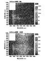
- FIG. 1 is a two-dimensional emission map obtained from the obtained oxidized SWCNT-SDBS heavy aqueous solution and the SWCNT-SDBS heavy aqueous solution before oxidation treatment (Fluorolog FL3-2TRIAX / iHR320, HORIBA).
- the vertical axis represents the excitation wavelength
- the horizontal axis represents the detection wavelength.
- an emission peak having an excitation wavelength of about 570 nm and an emission wavelength of about 980 nm mainly derived from the interband transition of the SWCNT having a chiral index (6, 5) is observed.
- the excitation wavelength did not change, and an emission peak whose emission wavelength was shifted to about 1280 nm was observed. This shift in the emission wavelength was caused by introducing oxygen atoms into SWCNT. It is because it was done.
- Example 2 the oxidation treatment time dependency of the emission intensity at 980 nm and 1280 nm of the sample centered on SWCNT having the above-mentioned chiral index (6, 5) was examined.
- FIG. 2 is a graph showing the dependency of the emission intensity on the oxidation treatment time.
- the 1280 nm emission (- ⁇ -) derived from oxidized SWCNT increases with a decrease in the 980 nm emission (- ⁇ -) accompanying the interband transition, and reaches a maximum in 180 seconds.
- strength decreases with the increase in reaction time after that. This decrease in emission intensity is presumed to be because the structure of SWCNT is broken by an excessive oxidation reaction.
- FIG. 3 is a two-dimensional emission map obtained from a SWCNT sample oxidized by the conventional method shown in Non-Patent Documents 1 and 2. Specifically, an oxygen / ozone mixed gas taken out from an ozone generator (SO-03UN-OX05, Hamanetsu) is passed through 3 mL of heavy water for about 1 minute, and the absorbance of an absorption peak at a wavelength of 260 nm derived from ozone is approximately Bubbling was performed until 1.0.
- an oxygen / ozone mixed gas taken out from an ozone generator SO-03UN-OX05, Hamanetsu
Landscapes
- Chemical & Material Sciences (AREA)
- Engineering & Computer Science (AREA)
- Health & Medical Sciences (AREA)
- Nanotechnology (AREA)
- Physics & Mathematics (AREA)
- Life Sciences & Earth Sciences (AREA)
- Organic Chemistry (AREA)
- Materials Engineering (AREA)
- General Health & Medical Sciences (AREA)
- General Physics & Mathematics (AREA)
- Immunology (AREA)
- Inorganic Chemistry (AREA)
- Biomedical Technology (AREA)
- Biochemistry (AREA)
- Pathology (AREA)
- Analytical Chemistry (AREA)
- Crystallography & Structural Chemistry (AREA)
- Molecular Biology (AREA)
- Hematology (AREA)
- Urology & Nephrology (AREA)
- Spectroscopy & Molecular Physics (AREA)
- Nuclear Medicine, Radiotherapy & Molecular Imaging (AREA)
- Toxicology (AREA)
- Electromagnetism (AREA)
- Chemical Kinetics & Catalysis (AREA)
- Biophysics (AREA)
- Condensed Matter Physics & Semiconductors (AREA)
- Manufacturing & Machinery (AREA)
- Optics & Photonics (AREA)
- Medicinal Chemistry (AREA)
- Food Science & Technology (AREA)
- Microbiology (AREA)
- Cell Biology (AREA)
- Biotechnology (AREA)
- Public Health (AREA)
- Veterinary Medicine (AREA)
- Animal Behavior & Ethology (AREA)
- Epidemiology (AREA)
- Carbon And Carbon Compounds (AREA)
- Luminescent Compositions (AREA)
Abstract
Description
[1]大気中で半導体単層カーボンナノチューブに直接紫外線を照射することにより、オゾンを発生させて半導体単層カーボンナノチューブを酸化処理することを特徴とする近赤外発光する半導体単層カーボンナノチューブの製造方法。
[2]前記紫外線を、基板上に薄膜状に形成された半導体単層カーボンナノチューブに照射することを特徴とする[1]に記載の近赤外発光する半導体単層カーボンナノチューブの製造方法。
[3]前記酸化処理を、密閉された空間で行うことを特徴とする[1]又は[2]に記載の近赤外発光する半導体単層カーボンナノチューブの製造方法。
[4][1]~[3]のいずれかの製造方法で製造された近赤外発光する半導体単層カーボンナノチューブであって、発光エネルギーが低エネルギーシフト化していることを特徴とする近赤外発光する半導体単層カーボンナノチューブ。
[5]発光エネルギーが296±10meV低エネルギーシフトしていることを特徴とする[4]に記載の近赤外発光する半導体単層カーボンナノチューブ。
[6]発光波長のピークが1280±13nm(=0.9686±0.01eV)にあることを特徴とする[4]又は[5]に記載の近赤外発光する半導体単層カーボンナノチューブ。
[7]半導体単層カーボンナノチューブに酸素原子が導入されている[4]~[6]のいずれかに記載の近赤外発光する半導体単層カーボンナノチューブ。
[8]前記酸素原子が主としてエポキシドとして導入されている[7]に記載の近赤外発光する半導体単層カーボンナノチューブ。
紫外線を照射する手法はSWCNTにも用いられており、例えば、特許文献1では、SWCNTに特定の単波長の光を照射して励起状態とし、励起状態にあるSWCNTを酸素で酸化させることにより、特定の構造のCNTを選択的に燃焼して消滅させ、該CNTとは異なる構造を有するCNTを選択的に得るとしている。
該非特許文献6の記述によれば、非特許文献1,2等の従来の湿式による方法では、ほとんどの酸素はSWCNTとエーテル結合しているために290meVを超える低エネルギーシフトが不可能であったが、本発明の方法によれば、導入された酸素はほとんどがSWCNTとエポキシドを形成し、これによりSWCNTの発光エネルギーを296±10meV低エネルギーシフトさせることが可能となったものと推定することができる。
また、紫外光の照射条件は、用いる装置によって異なるが、後述する実施例2のように、照射によりSWCNTが破壊されない条件下で行うことが必要である。
本実施例では、元試料に、CoMoCAT法により合成された、カイラル指数(6,5)をもつSWCNTが中心のものを用いた。
該SWCNT1.0mgを、直径47mmのメンブレンフィルター上に広げ、UVオゾンクリーナ(PC―450,Meiwafosis Co.,Ltd.)(光源:水銀ランプ、波長184.9、253.7nm等;電源:100V、0.5A)で0~600秒、酸化処理をおこなった。
その後、ナトリウムドデシルベンゼンスルホン酸塩(SDBS)0.1mgと重水10mL中で混合し、超音波処理(VIBRA-CELL VCX-500,Sonics and Materials Inc.)を10分間おこなうことで酸化SWCNTを分散させた。この分散液を1時間、超遠心処理(Himac CS100GXII,Hitachi Koki)(ローター:S52ST、回転数:35000rpm)した後、上澄み液中に存在する酸化SWCNTを取り出した。
図の上段に示すとおり、酸化処理前の試料においては、カイラル指数(6,5)のSWCNTのバンド間遷移に由来する励起波長約570nm、発光波長約980nmの発光ピークが主に観測される。一方、図の下段に示すとおり、180秒処理したものでは、励起波長は変わらず、発光波長が約1280nmに長波長シフトした発光ピークが観測され、この発光波長のシフトはSWCNTに酸素原子が導入されたことによるものである。
本実施例では、前述のカイラル指数(6,5)をもつSWCNTが中心の試料の980nmと1280nmの発光強度の、酸化処理時間依存性を調べた。
図2は、発光強度の酸化処理時間依存性を示す図であり、縦軸は発光強度、横軸は照射時間である。
図2に示すとおり、酸化SWCNT由来の1280nm発光(-●-)は、バンド間遷移に伴う980nm発光(-▲-)の減少と共に増加し、180秒で極大に達する。そして、その後反応時間の増大と共に強度が減少する。この発光強度減少は過度な酸化反応によってSWCNTの構造が壊されていっているためと推測される。
図3は、非特許文献1、2で示されている従来法によって酸化処理したSWCNT試料から得られた2次元発光マップである。
具体的には、オゾン発生器(SO-03UN-OX05,Hamanetsu)より取り出した酸素・オゾン混合ガスを、3mLの重水中に約1分間通し、オゾンに由来する波長260nmの吸収ピークの吸光度がおよそ1.0になるまでバブリングした。このオゾン含有重水2mLと、SWCNTを1重量%SDBS重水溶液に分散し、超遠心処理によって得られた上澄み溶液400μL、重水1.6mLを混合し、波長254nmの紫外光をトランスイルミネータ(CSF-20AC,コスモバイオ)(強度:6400μW/cm2)で1分間照射し、酸化SWCNT溶液を得た。
図3に示すとおり、従来法で調整した酸化SWCNT溶液では、酸化処理により、主として約1140nm(約1.088eV)の発光が観察され、酸素がSWCNT壁にエーテル結合していると推測される。
また、この方法では、混合するオゾン水の量、光照射の時間や波長を変更しても、実施例1のような、SWCNTと酸素をエポキシド化させたことに由来すると推測される1280nmの発光のピークの増大は確認できなかった。
Claims (8)
- 大気中で半導体単層カーボンナノチューブに直接紫外線を照射することにより、オゾンを発生させて半導体単層カーボンナノチューブを酸化処理することを特徴とする近赤外発光する半導体単層カーボンナノチューブの製造方法。
- 前記紫外線を、基板上に薄膜状に形成された半導体単層カーボンナノチューブに照射することを特徴とする請求項1に記載の近赤外発光する半導体単層カーボンナノチューブの製造方法。
- 前記酸化処理を、密閉された空間で行うことを特徴とする請求項1又は2に記載の近赤外発光する半導体単層カーボンナノチューブの製造方法。
- 請求項1~3のいずれか1項に記載の製造方法で製造された近赤外発光する半導体単層カーボンナノチューブであって、発光エネルギーが低エネルギーシフト化していることを特徴とする近赤外発光する半導体単層カーボンナノチューブ。
- 発光エネルギーが296±10meV低エネルギーシフトしていることを特徴とする請求項4に記載の近赤外発光する半導体単層カーボンナノチューブ。
- 発光波長のピークが1280±13nmにあることを特徴とする請求項4又は5に記載の近赤外発光する半導体単層カーボンナノチューブ。
- 半導体単層カーボンナノチューブに酸素原子が導入されている請求項4~6のいずれか1項に記載の近赤外発光する半導体単層カーボンナノチューブ。
- 前記酸素原子が主としてエポキシドとして導入されている請求項7に記載の近赤外発光する半導体単層カーボンナノチューブ。
Priority Applications (4)
| Application Number | Priority Date | Filing Date | Title |
|---|---|---|---|
| KR1020177023208A KR102050147B1 (ko) | 2015-01-23 | 2016-01-21 | 근적외선을 발광하는 반도체 단층 카본 나노 튜브 |
| CN201680006878.3A CN107614427B (zh) | 2015-01-23 | 2016-01-21 | 近红外发光的半导体单层碳纳米管 |
| JP2016570694A JP6548230B2 (ja) | 2015-01-23 | 2016-01-21 | 近赤外発光する半導体単層カーボンナノチューブ |
| US15/657,543 US10752835B2 (en) | 2015-01-23 | 2017-07-24 | Dispersion solution of semiconductor single-layer carbon nanotube |
Applications Claiming Priority (2)
| Application Number | Priority Date | Filing Date | Title |
|---|---|---|---|
| JP2015-011582 | 2015-01-23 | ||
| JP2015011582 | 2015-01-23 |
Related Child Applications (1)
| Application Number | Title | Priority Date | Filing Date |
|---|---|---|---|
| US15/657,543 Continuation US10752835B2 (en) | 2015-01-23 | 2017-07-24 | Dispersion solution of semiconductor single-layer carbon nanotube |
Publications (1)
| Publication Number | Publication Date |
|---|---|
| WO2016117633A1 true WO2016117633A1 (ja) | 2016-07-28 |
Family
ID=56417165
Family Applications (1)
| Application Number | Title | Priority Date | Filing Date |
|---|---|---|---|
| PCT/JP2016/051660 Ceased WO2016117633A1 (ja) | 2015-01-23 | 2016-01-21 | 近赤外発光する半導体単層カーボンナノチューブ |
Country Status (5)
| Country | Link |
|---|---|
| US (1) | US10752835B2 (ja) |
| JP (1) | JP6548230B2 (ja) |
| KR (1) | KR102050147B1 (ja) |
| CN (1) | CN107614427B (ja) |
| WO (1) | WO2016117633A1 (ja) |
Cited By (2)
| Publication number | Priority date | Publication date | Assignee | Title |
|---|---|---|---|---|
| WO2019097697A1 (ja) * | 2017-11-17 | 2019-05-23 | 株式会社島津製作所 | 生体イメージング用半導体swcnt分散液及びその製造方法 |
| CN111356481A (zh) * | 2017-11-17 | 2020-06-30 | 株式会社岛津制作所 | 生物成像用半导体swcnt分散液及其检查方法 |
Families Citing this family (2)
| Publication number | Priority date | Publication date | Assignee | Title |
|---|---|---|---|---|
| JP7002517B2 (ja) * | 2019-11-15 | 2022-01-20 | 花王株式会社 | 半導体型単層カーボンナノチューブ分散液の製造方法 |
| JP6900453B2 (ja) * | 2019-11-15 | 2021-07-07 | 花王株式会社 | 半導体型単層カーボンナノチューブ分散液の製造方法 |
Citations (3)
| Publication number | Priority date | Publication date | Assignee | Title |
|---|---|---|---|---|
| JP2004210608A (ja) * | 2003-01-06 | 2004-07-29 | Japan Science & Technology Agency | 光照射によるカーボンナノチューブの構造選択法 |
| JP2008285387A (ja) * | 2007-05-21 | 2008-11-27 | National Institute Of Advanced Industrial & Technology | カーボンナノチューブの高効率分離法 |
| JP2008285386A (ja) * | 2007-05-21 | 2008-11-27 | National Institute Of Advanced Industrial & Technology | カーボンナノチューブの分離法 |
-
2016
- 2016-01-21 JP JP2016570694A patent/JP6548230B2/ja active Active
- 2016-01-21 WO PCT/JP2016/051660 patent/WO2016117633A1/ja not_active Ceased
- 2016-01-21 KR KR1020177023208A patent/KR102050147B1/ko active Active
- 2016-01-21 CN CN201680006878.3A patent/CN107614427B/zh active Active
-
2017
- 2017-07-24 US US15/657,543 patent/US10752835B2/en active Active
Patent Citations (3)
| Publication number | Priority date | Publication date | Assignee | Title |
|---|---|---|---|---|
| JP2004210608A (ja) * | 2003-01-06 | 2004-07-29 | Japan Science & Technology Agency | 光照射によるカーボンナノチューブの構造選択法 |
| JP2008285387A (ja) * | 2007-05-21 | 2008-11-27 | National Institute Of Advanced Industrial & Technology | カーボンナノチューブの高効率分離法 |
| JP2008285386A (ja) * | 2007-05-21 | 2008-11-27 | National Institute Of Advanced Industrial & Technology | カーボンナノチューブの分離法 |
Non-Patent Citations (2)
| Title |
|---|
| SAUNAB GHOSH ET AL., SCIENCE, vol. 330, 2010, pages 1656 - 1659 * |
| YUHEI MIYAUCHI ET AL., NATURE PHOTONICS, vol. 7, 2013, pages 715 - 719 * |
Cited By (9)
| Publication number | Priority date | Publication date | Assignee | Title |
|---|---|---|---|---|
| WO2019097697A1 (ja) * | 2017-11-17 | 2019-05-23 | 株式会社島津製作所 | 生体イメージング用半導体swcnt分散液及びその製造方法 |
| CN111356481A (zh) * | 2017-11-17 | 2020-06-30 | 株式会社岛津制作所 | 生物成像用半导体swcnt分散液及其检查方法 |
| CN111432846A (zh) * | 2017-11-17 | 2020-07-17 | 株式会社岛津制作所 | 生物成像用半导体swcnt分散液及其制造方法 |
| JPWO2019097697A1 (ja) * | 2017-11-17 | 2020-12-17 | 株式会社島津製作所 | 生体イメージング用半導体swcnt分散液及びその製造方法 |
| JPWO2019097698A1 (ja) * | 2017-11-17 | 2020-12-24 | 株式会社島津製作所 | 生体イメージング用半導体swcnt分散液及びその検査方法 |
| JP7100856B2 (ja) | 2017-11-17 | 2022-07-14 | 株式会社島津製作所 | 生体イメージング用半導体swcnt分散液及びその製造方法 |
| JP7100857B2 (ja) | 2017-11-17 | 2022-07-14 | 株式会社島津製作所 | 生体イメージング用半導体swcnt分散液及びその検査方法 |
| US11696688B2 (en) | 2017-11-17 | 2023-07-11 | Shimadzu Corporation | Semiconductor SWCNT slurry for bioimaging and method for producing the same |
| US12257324B2 (en) | 2017-11-17 | 2025-03-25 | Shimadzu Corporation | Semiconductor SWCNT slurry for bioimaging and method for inspecting the same |
Also Published As
| Publication number | Publication date |
|---|---|
| CN107614427A (zh) | 2018-01-19 |
| JP6548230B2 (ja) | 2019-07-24 |
| CN107614427B (zh) | 2020-06-23 |
| JPWO2016117633A1 (ja) | 2017-12-07 |
| US20170335185A1 (en) | 2017-11-23 |
| KR102050147B1 (ko) | 2019-11-28 |
| KR20170107020A (ko) | 2017-09-22 |
| US10752835B2 (en) | 2020-08-25 |
Similar Documents
| Publication | Publication Date | Title |
|---|---|---|
| Zhou et al. | Carbon nitride nanotubes with in situ grafted hydroxyl groups for highly efficient spontaneous H2O2 production | |
| Rosales et al. | The influence of the morphology of 1D TiO2 nanostructures on photogeneration of reactive oxygen species and enhanced photocatalytic activity | |
| Qu et al. | Photochemical transformation of carboxylated multiwalled carbon nanotubes: role of reactive oxygen species | |
| Yang et al. | Influence of pH on the fluorescence properties of graphene quantum dots using ozonation pre-oxide hydrothermal synthesis | |
| Mallakpour et al. | Synthesis of alginate/carbon nanotube/carbon dot/fluoroapatite/TiO2 beads for dye photocatalytic degradation under ultraviolet light | |
| Xiao et al. | Dramatic coupling of visible light with ozone on honeycomb-like porous g-C3N4 towards superior oxidation of water pollutants | |
| Ali et al. | Role of reactive oxygen species in the visible light photocatalytic mineralization of rhodamine B dye by P25–carbon dot photocatalyst | |
| Altin | CuO-TiO2/graphene ternary nanocomposite for highly efficient visible-light-driven photocatalytic degradation of bisphenol A | |
| Shen et al. | Double-walled carbon nanotubes: challenges and opportunities | |
| JP6548230B2 (ja) | 近赤外発光する半導体単層カーボンナノチューブ | |
| Mamba et al. | Nd, N, S-TiO2 decorated on reduced graphene oxide for a visible light active photocatalyst for dye degradation: Comparison to its MWCNT/Nd, N, S-TiO2 analogue | |
| Checa et al. | Graphene oxide/titania photocatalytic ozonation of primidone in a visible LED photoreactor | |
| Razdyakonova et al. | Influence of environmental conditions on carbon black oxidation by reactive oxygen intermediates | |
| Ortega-Liébana et al. | Nitrogen-doped luminescent carbon nanodots for optimal photo-generation of hydroxyl radicals and visible-light expanded photo-catalysis | |
| Orge et al. | Photocatalytic ozonation of model aqueous solutions of oxalic and oxamic acids | |
| Lopes et al. | Outstanding response of carbon nitride photocatalysts for selective synthesis of aldehydes under UV-LED irradiation | |
| Uma et al. | Enriched silver plasmon resonance activity on the sonochemical synthesis of ZnO flowers with α-Fe2O3 as an efficient catalyst for photo-Fenton reaction and photo-oxidation of ethanol | |
| Kim et al. | Solution Plasma‐Assisted Green Synthesis of MnO2 Adsorbent and Removal of Cationic Pollutant | |
| Sartori et al. | Multi-walled carbon nanotubes photochemistry: A mechanistic view of the effect of impurities and oxygen-containing surface groups | |
| Maeda et al. | Sonochemical reaction to control the near-infrared photoluminescence properties of single-walled carbon nanotubes | |
| Panigrahy et al. | Minuscule weight percent of graphene oxide and reduced graphene oxide modified Ag 3 PO 4: new insight into improved photocatalytic activity | |
| Pagel et al. | Carbon quantum dot-decorated zirconia nanoparticles for photo-and sonocatalytic dye degradation | |
| Zhu et al. | Investigation of reactive oxygen species produced by microwave electrodeless discharge lamp on oxidation of dimethyl sulfide | |
| JP2021195272A (ja) | 単層グラフェンシート及びこれを用いた化学センサー並びに単層グラフェンシートの処理方法 | |
| Mohamed et al. | Compare studies for the photocatalytic degradation of thymol blue with synthesized and commercial MWCNTs |
Legal Events
| Date | Code | Title | Description |
|---|---|---|---|
| 121 | Ep: the epo has been informed by wipo that ep was designated in this application |
Ref document number: 16740240 Country of ref document: EP Kind code of ref document: A1 |
|
| ENP | Entry into the national phase |
Ref document number: 2016570694 Country of ref document: JP Kind code of ref document: A |
|
| NENP | Non-entry into the national phase |
Ref country code: DE |
|
| ENP | Entry into the national phase |
Ref document number: 20177023208 Country of ref document: KR Kind code of ref document: A |
|
| 122 | Ep: pct application non-entry in european phase |
Ref document number: 16740240 Country of ref document: EP Kind code of ref document: A1 |