WO2016114225A1 - 有機蒸着膜の製造方法及び有機エレクトロルミネッセンス装置 - Google Patents
有機蒸着膜の製造方法及び有機エレクトロルミネッセンス装置 Download PDFInfo
- Publication number
- WO2016114225A1 WO2016114225A1 PCT/JP2016/050441 JP2016050441W WO2016114225A1 WO 2016114225 A1 WO2016114225 A1 WO 2016114225A1 JP 2016050441 W JP2016050441 W JP 2016050441W WO 2016114225 A1 WO2016114225 A1 WO 2016114225A1
- Authority
- WO
- WIPO (PCT)
- Prior art keywords
- vapor deposition
- organic
- organic vapor
- release rate
- chamber
- Prior art date
- Legal status (The legal status is an assumption and is not a legal conclusion. Google has not performed a legal analysis and makes no representation as to the accuracy of the status listed.)
- Ceased
Links
Images




Classifications
-
- C—CHEMISTRY; METALLURGY
- C23—COATING METALLIC MATERIAL; COATING MATERIAL WITH METALLIC MATERIAL; CHEMICAL SURFACE TREATMENT; DIFFUSION TREATMENT OF METALLIC MATERIAL; COATING BY VACUUM EVAPORATION, BY SPUTTERING, BY ION IMPLANTATION OR BY CHEMICAL VAPOUR DEPOSITION, IN GENERAL; INHIBITING CORROSION OF METALLIC MATERIAL OR INCRUSTATION IN GENERAL
- C23C—COATING METALLIC MATERIAL; COATING MATERIAL WITH METALLIC MATERIAL; SURFACE TREATMENT OF METALLIC MATERIAL BY DIFFUSION INTO THE SURFACE, BY CHEMICAL CONVERSION OR SUBSTITUTION; COATING BY VACUUM EVAPORATION, BY SPUTTERING, BY ION IMPLANTATION OR BY CHEMICAL VAPOUR DEPOSITION, IN GENERAL
- C23C14/00—Coating by vacuum evaporation, by sputtering or by ion implantation of the coating forming material
- C23C14/06—Coating by vacuum evaporation, by sputtering or by ion implantation of the coating forming material characterised by the coating material
- C23C14/12—Organic material
-
- C—CHEMISTRY; METALLURGY
- C23—COATING METALLIC MATERIAL; COATING MATERIAL WITH METALLIC MATERIAL; CHEMICAL SURFACE TREATMENT; DIFFUSION TREATMENT OF METALLIC MATERIAL; COATING BY VACUUM EVAPORATION, BY SPUTTERING, BY ION IMPLANTATION OR BY CHEMICAL VAPOUR DEPOSITION, IN GENERAL; INHIBITING CORROSION OF METALLIC MATERIAL OR INCRUSTATION IN GENERAL
- C23C—COATING METALLIC MATERIAL; COATING MATERIAL WITH METALLIC MATERIAL; SURFACE TREATMENT OF METALLIC MATERIAL BY DIFFUSION INTO THE SURFACE, BY CHEMICAL CONVERSION OR SUBSTITUTION; COATING BY VACUUM EVAPORATION, BY SPUTTERING, BY ION IMPLANTATION OR BY CHEMICAL VAPOUR DEPOSITION, IN GENERAL
- C23C14/00—Coating by vacuum evaporation, by sputtering or by ion implantation of the coating forming material
- C23C14/22—Coating by vacuum evaporation, by sputtering or by ion implantation of the coating forming material characterised by the process of coating
- C23C14/24—Vacuum evaporation
-
- C—CHEMISTRY; METALLURGY
- C23—COATING METALLIC MATERIAL; COATING MATERIAL WITH METALLIC MATERIAL; CHEMICAL SURFACE TREATMENT; DIFFUSION TREATMENT OF METALLIC MATERIAL; COATING BY VACUUM EVAPORATION, BY SPUTTERING, BY ION IMPLANTATION OR BY CHEMICAL VAPOUR DEPOSITION, IN GENERAL; INHIBITING CORROSION OF METALLIC MATERIAL OR INCRUSTATION IN GENERAL
- C23C—COATING METALLIC MATERIAL; COATING MATERIAL WITH METALLIC MATERIAL; SURFACE TREATMENT OF METALLIC MATERIAL BY DIFFUSION INTO THE SURFACE, BY CHEMICAL CONVERSION OR SUBSTITUTION; COATING BY VACUUM EVAPORATION, BY SPUTTERING, BY ION IMPLANTATION OR BY CHEMICAL VAPOUR DEPOSITION, IN GENERAL
- C23C14/00—Coating by vacuum evaporation, by sputtering or by ion implantation of the coating forming material
- C23C14/22—Coating by vacuum evaporation, by sputtering or by ion implantation of the coating forming material characterised by the process of coating
- C23C14/54—Controlling or regulating the coating process
-
- H—ELECTRICITY
- H05—ELECTRIC TECHNIQUES NOT OTHERWISE PROVIDED FOR
- H05B—ELECTRIC HEATING; ELECTRIC LIGHT SOURCES NOT OTHERWISE PROVIDED FOR; CIRCUIT ARRANGEMENTS FOR ELECTRIC LIGHT SOURCES, IN GENERAL
- H05B33/00—Electroluminescent light sources
- H05B33/10—Apparatus or processes specially adapted to the manufacture of electroluminescent light sources
-
- H—ELECTRICITY
- H10—SEMICONDUCTOR DEVICES; ELECTRIC SOLID-STATE DEVICES NOT OTHERWISE PROVIDED FOR
- H10K—ORGANIC ELECTRIC SOLID-STATE DEVICES
- H10K50/00—Organic light-emitting devices
- H10K50/10—OLEDs or polymer light-emitting diodes [PLED]
- H10K50/11—OLEDs or polymer light-emitting diodes [PLED] characterised by the electroluminescent [EL] layers
Definitions
- the present invention relates to a method for producing an organic vapor-deposited film and an organic electroluminescence device having an organic vapor-deposited film formed by the production method.
- the vapor deposition method is a method in which a vapor deposition material (for example, a metal oxide or an organic compound) contained in a vapor deposition source is heated and vaporized, and the vaporized vapor deposition material is attached to the surface of a substrate. It refers to a method of forming a thin film of vapor deposition material (vapor deposition film) on the surface of the material.
- a co-evaporation method is known as one of the evaporation methods.
- vapor deposition films containing two or more vapor deposition materials are formed on the surface of a substrate by simultaneously heating different vapor deposition materials contained in two or more vapor deposition sources provided in a vacuum chamber. It is a method to do.
- the co-evaporation method is used in various technical fields.
- an organic electroluminescence device is known in which an organic vapor deposition film is formed by co-evaporation of a host material, which is a vapor deposition material (organic vapor deposition material) containing an organic compound, and a dopant material, and this organic vapor deposition film is used as a light emitting layer.
- Patent Document 1 an organic electroluminescence device is known in which an organic vapor deposition film is formed by co-evaporation of a host material, which is a vapor deposition material (organic vapor deposition material) containing an organic compound, and a dopant material, and this organic vapor deposition film is used as a light emitting layer.
- a release rate sensor corresponding to each deposition source is usually provided in the chamber, and the deposition amount of each deposition material is estimated based on the measurement value of the release rate sensor.
- the deposition amount of each deposition material is estimated based on the value of the emission rate sensor, it is difficult to accurately deposit the desired amount of each deposition material on the surface of the substrate. This is particularly noticeable when using materials.
- the ratio of each organic vapor deposition material contained in the obtained organic vapor deposition film naturally does not become a desired value. As a result, there is a problem that the functionality of the obtained organic vapor deposition film is lowered. For example, in the light emitting layer, when the host material and the dopant material are not contained in a desired ratio, the light emitting function of the organic electroluminescence device is lowered, which causes uneven color.
- An object of the present invention is to provide an organic vapor-deposited film manufacturing method capable of accurately controlling the vapor deposition amount of each organic vapor-deposited material, and an organic electroluminescence device having an organic vapor-deposited film excellent in light emitting function as a light-emitting layer.
- the inventors have difficulty in accurately depositing a desired amount of each organic vapor deposition material.
- One reason is that a part of the vaporized organic vapor deposition material is provided corresponding to each vapor deposition source. It was discovered that this is because it affects the measured value.
- FIG. In the present invention, a plurality of vapor deposition sources and release rate sensors are used. Therefore, in this specification, in order to distinguish each vapor deposition source and each discharge rate sensor, a lower case alphabet such as “a” or “b” may be appended to the reference numerals.
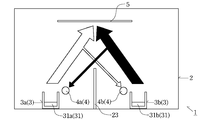
- FIG. 1 is a schematic diagram of a general vapor deposition film manufacturing apparatus 1.
- a vapor deposition source 3 including an organic vapor deposition material 31 is provided in the chamber 2 of the vapor deposition film manufacturing apparatus 1.
- the arrow indicates the flow path of the organic vapor deposition material 31 in the vacuum chamber 2, and the thickness of the arrow reflects the flow rate of the organic vapor deposition material 31.
- a white arrow represents a flow path and a flow rate of a first organic vapor deposition material 31a described later, and a black arrow represents a flow path and a flow rate of a second organic vapor deposition material 31b described later.
- FIG. 1 is a schematic diagram of a general vapor deposition film manufacturing apparatus 1.
- a vapor deposition source 3 including an organic vapor deposition material 31 is provided in the chamber 2 of the vapor deposition film manufacturing apparatus 1.
- the arrow indicates the flow path of the organic vapor deposition material 31 in the vacuum chamber 2
- the thickness of the arrow reflects the flow rate of
- a first vapor deposition source 3 a and a second vapor deposition source 3 b are provided in the vacuum chamber 2.
- the 1st vapor deposition source 3a contains the 1st organic vapor deposition material 31a
- the 2nd vapor deposition source 3b contains the 2nd organic vapor deposition material 31b.
- a first release rate sensor 4 a that measures the rate (release rate) at which the first organic vapor deposition material 31 a is released into the chamber 2 is provided corresponding to the first vapor deposition source 3 a
- a second release rate sensor 4b for measuring the release rate of the second organic vapor deposition material 31b is provided corresponding to the second vapor deposition source 3b.
- a partition between the first and second vapor deposition sources 3a and 3b is provided so that the first organic vapor deposition material 31a or the second organic vapor deposition material 31b is not mixed into the second emission rate sensor 4b or the first emission rate sensor 4a. 23 is provided.
- the vaporized first and second organic vapor deposition materials 31a and 31b are directed toward the base material 5 to be vapor deposited. Released (see thick arrows).
- the partition wall 23 since the first and second organic vapor deposition materials 31a and 31b are vaporized in the chamber 2, a part of the first organic vapor deposition material 31a exceeds the partition wall 23 to the second Similarly, a part of the second organic vapor deposition material 31b wraps around the partition wall 23 toward the first vapor deposition source 3a (see each thin arrow). Therefore, mixing cannot be prevented completely.
- a part of the first organic vapor deposition material 31a or a part of the second organic vapor deposition material 31b wrapping around the partition wall 23 is a second emission rate sensor corresponding to the second vapor deposition source 3b or the first vapor deposition source 3a. Since it adheres to 4b or the 1st discharge
- each organic vapor deposition material 31a, 31b is vapor-deposited at a desired release rate, the measured value of each emission rate sensor 4a, 4b does not reflect the true emission rate of each organic vapor deposition material 31a, 31b. It becomes difficult to control the amount of vapor deposition of the organic vapor deposition materials 31a and 31b on the base material 5. The inventors have thus discovered that each vaporized organic vapor deposition material affects not only the corresponding emission rate sensor readings, but also the measurements of all emission rate sensors present in the chamber. did.
- the inventors have found that the mixing rate of each organic vapor deposition material with respect to each emission rate sensor is substantially constant regardless of the amount of each organic vapor deposition material released, and all the vapor deposition sources.
- the present invention was completed by finding the law that the mixing rate is substantially constant even if the two are simultaneously heated.
- the method for producing an organic vapor deposition film of the present invention includes a chamber in which the inside is maintained in a vacuum state, n vapor deposition sources including an organic vapor deposition material discharged into the chamber, and the n vapor deposition sources corresponding to the n vapor deposition sources.
- Preparation step of preparing a vapor deposition film manufacturing apparatus having n release rate sensors for measuring the release rate of the organic vapor deposition material, and mixing of each organic vapor deposition material into each emission rate sensor using the vapor deposition film manufacturing apparatus A pre-process for calculating the rate, and a vapor deposition process for forming an organic vapor deposition film on the surface of the substrate introduced into the chamber by simultaneously discharging all the organic vapor deposition materials into the chamber, A first step of heating only one jth vapor deposition source selected from the n vapor deposition sources and releasing a jth organic vapor deposition material contained in the jth vapor deposition source into the chamber; Before the first Based on the measured value of the j-release rate sensor corresponding to the j-th deposition source was heated with degree (PMV j) and the i measurements of release rate sensor corresponding to the i deposition source (PMV i), the following equation ( A second pre-process for calculating the mixing rate (CR ij ) of the
- the true emission rate of each organic vapor deposition material using the mixing rate of all organic vapor deposition materials with respect to the rate sensor and the measured value of each emission rate sensor detected in the first vapor deposition step.
- each of the n vapor deposition sources has a container containing an organic vapor deposition material, and the chamber has a discharge port inside thereof.
- a mixing chamber, and each container of the n deposition sources communicates with the mixing chamber, and in the deposition step, the organic deposition materials contained in the n deposition sources are mixed with each other.
- the mixed organic vapor deposition material is discharged from the discharge port toward the surface of the substrate.
- each container of the n vapor deposition sources communicates with the mixing chamber via a cylindrical member having a cavity through which the vaporized organic vapor deposition material can pass.
- the tubular member has a valve portion that can arbitrarily change the width of the hollow portion.
- the organic vapor deposition film manufacturing method of the present invention feedback-controls the discharge conditions of each organic vapor deposition material by changing the heating temperature of each vapor deposition source in the third vapor deposition step.
- the discharge condition of each organic vapor deposition material is feedback controlled by changing the width of the cavity portion using the valve portion. To do.
- the distance between the discharge port of the mixing chamber and the base material is 10 mm or less.
- the degree of vacuum in the chamber is 10 ⁇ 3 Pa or less.
- an organic electroluminescence device is provided.
- the organic electroluminescence device of the present invention has an organic vapor deposition film formed by the above-described method for producing an organic vapor deposition film as a light emitting layer.
- each organic vapor deposition material can be released into the chamber at a desired release rate, so that the amount of each organic vapor deposition material deposited on the substrate can be accurately controlled.
- An organic vapor deposition film containing the material in a desired ratio can be formed.
- the organic electroluminescent apparatus of this invention has an organic vapor deposition film containing each organic vapor deposition material by the desired ratio as a light emitting layer, it is excellent in a light emission function.
- the reference figure showing the flow path of the organic vapor deposition material in a chamber.
- (A) is a graph in which measured values of the respective emission rate sensors are plotted over time when only the first vapor deposition source is heated, and (b) is for each emission rate sensor when only the first vapor deposition source is heated.
- the graph which plotted the mixing rate of the 1st organic vapor deposition material with time.
- (A) is a graph in which measured values of the respective release rate sensors are plotted over time when only the second vapor deposition source is heated, and (b) is for each emission rate sensor when only the second vapor deposition source is heated.
- the graph which plotted the mixing rate of the 2nd organic vapor deposition material with time (A) is a graph in which measured values of the respective emission rate sensors are plotted over time when the first and second vapor deposition sources are heated, and (b) is a graph of FIGS. 3 (a) and 4 (a). A graph that combines the measured values of the release rate sensor.
- (A) is the graph which plotted the measured value of each discharge rate sensor in the case where only the 1st vapor deposition source was heated in the example, and (b) is each graph when only the 1st vapor deposition source was heated.
- (A) is the graph which plotted the measured value of each discharge rate sensor in the case where only the 2nd vapor deposition source was heated in the example, and (b) is each graph when only the 2nd vapor deposition source was heated.
- the graph which plotted the mixing rate of the 2nd organic vapor deposition material with respect to a discharge rate sensor with time is the graph which plotted the measured value of each discharge rate sensor in the case where only the 2nd vapor deposition source was heated in the example.
- (A) is the graph which plotted the measured value of each discharge rate sensor in the case where only the 3rd vapor deposition source was heated in the example, and (b) is each graph when only the 3rd vapor deposition source was heated.
- (A) is a graph in which the true emission rate of each organic vapor deposition material and the measured value of each emission rate sensor are plotted over time in the example, and (b) is a graph of each emission rate sensor from the graph of (a). Graph excluding measured values.
- the manufacturing method of the organic vapor deposition film of this invention has a preparatory process, a pre-process, and a vapor deposition process.
- the preparation step is a step of preparing a vapor deposition film manufacturing apparatus
- the previous step is a step of calculating the mixing rate of each organic vapor deposition material with respect to each emission rate sensor
- the vapor deposition step is an organic vapor deposition material on the surface of the substrate. Is a step of co-evaporation.
- the preparation process, the pre-process, and the vapor deposition process are performed in this order.
- each step will be described.
- a preparation process is a process of preparing a vapor deposition film manufacturing apparatus.
- Vapor deposition film manufacturing equipment measures the emission rate of organic vapor deposition material corresponding to n vapor deposition sources including the chamber which kept the inside in a vacuum state, the organic vapor deposition material released into the chamber, and the n vapor deposition sources N release rate sensors.
- Each of the n deposition sources includes a different organic deposition material.
- n is a natural number of 2 or more, and the value of n can be appropriately changed according to the number of types of organic vapor deposition materials to be co-deposited.
- each of the n deposition sources includes a different type of organic vapor deposition material
- n types of organic vapor deposition materials are used.
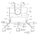
- the present invention will be described using the vapor deposition film manufacturing apparatus according to the first embodiment of the present invention shown in FIG. 2 as an example.
- 2 has two vapor deposition sources 3a and 3b (that is, two kinds of organic vapor deposition materials 31a and 31b are used).
- the number of vapor deposition sources 3 is as follows. It is not limited to two. Further, the structure of the chamber 2 and the vapor deposition source 3 is not limited to this embodiment.
- the chamber 2 is a housing capable of maintaining the inside thereof in a vacuum state.
- a vacuum pump (not shown) is connected to the chamber 2, and the inside of the chamber 2 is depressurized by using this vacuum pump, and the vacuum state is maintained.
- the upper limit of the degree of vacuum in the chamber 2 is not particularly limited, but is preferably 10 ⁇ 3 Pa (that is, 0.001 Pa), and more preferably 10 ⁇ 4 Pa (that is, 0.0001 Pa).
- the lower limit value of the degree of vacuum is not particularly limited, but is 10 ⁇ 6 Pa (that is, 0.000001 Pa), preferably 10 ⁇ 5 Pa (that is, 0.00001 Pa) from a practical viewpoint.
- each organic vapor deposition material 31a, 31b released into the chamber 2 The higher the degree of vacuum, the longer the mean free path of each organic vapor deposition material 31a, 31b released into the chamber 2, and the more difficult the organic vapor deposition materials 31a, 31b interfere with each other in the chamber 2.
- the true emission rate of each of the organic vapor deposition materials 31a and 31b can be calculated accurately (specifically, it will be described in the section of the previous step described later).
- the inside of the chamber 2 is partitioned into a vapor deposition area 21 and a non-vapor deposition area 22 by a first partition wall 231 that is installed in the horizontal direction.
- the vapor deposition area 21 is an area where the organic vapor deposition materials 31a and 31b are vapor-deposited on the base material 5, and is an area filled with the organic vapor deposition materials 31a and 31b in the vapor deposition process.
- the non-deposition area is an area where the base material 5 is not deposited, and is an area where the organic deposition materials 31a and 31b hardly exist in the deposition process.
- the first partition 231 has a hole communicating from the vapor deposition area 21 to the non-vapor deposition area 22, and the base material 5 is introduced from the non-vapor deposition area 21 to the vapor deposition area 22 through the hole.
- the second partition 232 is erected in order to prevent the organic vapor deposition materials 31a and 31b from being mixed between the release rate sensors 4a and 4b.
- the first partition 231 and the second partition 232 are not necessarily provided. But when the 2nd partition 232 does not exist, the amount of each organic vapor deposition material 31a, 31b mixed with each discharge
- the base material 5 has a long shape and is wound around a first roll A outside the chamber 2.
- the wound base material 5 is fed out and sequentially introduced into the chamber 2 to form an organic vapor deposition film on the surface of the base material 5.
- the base material 5 fed out from the first roll A is introduced into the non-deposition area 22 in the chamber 2, and then the non-deposition area 22 and the evaporation area 21 through the holes of the first partition 231. It is introduced into the vapor deposition area 21 by the second roll B straddling it. Thereafter, the substrate 5 is again introduced into the non-deposition area 22 and is wound around the third roll C outside the chamber 2 again.
- the substrate 5 is co-deposited with the organic vapor deposition materials 31 a and 31 b only while it is exposed to the vapor deposition area 21.
- the arrow represents the feeding direction of the substrate 5.
- the base material 5 is introduced into the chamber 2, but the base material 5 does not have to be introduced into the chamber 2 at the stage of the preparation process and the previous process described later.
- the vapor deposition source 3 includes an organic vapor deposition material 31 and a container 32 that accommodates the organic vapor deposition material 31.
- the container 32 has an opening 321 that opens toward the inside of the chamber 2 at an upper portion thereof.
- the container 32 may be provided with a shutter for adjusting the opening degree of the opening 321 (not shown).
- the shutter is a member that can adjust the discharge amount of the organic vapor deposition material 31 by covering the opening 321.
- the area where the shutter covers the opening 321 can be arbitrarily changed.
- the container 32 is not particularly limited as long as it has heat resistance. For example, a crucible made of aluminum oxide, boron nitride, or the like can be used.
- the organic vapor deposition material 31 housed in the container is indirectly heated.
- the heated organic vapor deposition material 31 is vaporized and discharged into the chamber 2 through the opening 321 of the container 32.
- the method of heating the vapor deposition source 3 is not specifically limited, For example, the resistance heating system using the wire heater etc. which used the infrared lamp, the metal wires, such as tungsten and tantalum, etc. are used. .
- a metal wire is wound around the outer peripheral surface of the container 32 (not shown).
- the number of vapor deposition sources 3 is equal to the number of types of organic vapor deposition materials 31, and the number thereof is n.
- the organic vapor deposition film formed with this vapor deposition film manufacturing apparatus 1 is 2 types.
- Organic vapor deposition materials 31a and 31b are included.
- the organic vapor deposition material is a vapor deposition material containing an organic compound, and is preferably a vapor deposition material consisting essentially of an organic compound.
- “consisting essentially of an organic compound” includes not only the case of completely consisting of an organic compound, but also includes the case where a compound other than an organic compound is contained within a range not impairing the effects of the present invention, For example, the case where the ratio of the organic compound in the whole organic vapor deposition material is 98 mass% or more is included.
- the organic compound contained in the organic vapor deposition material is not particularly limited, and can be appropriately selected according to the use of the vapor deposition film.
- An organic compound is a compound having a carbon atom in the basic skeleton of the structure (however, carbon monoxide, carbon dioxide, metal carbonate, hydrocyanic acid, metal cyanate, metal cyanate, metal thiocyanate, other history) Excluding those treated as inorganic compounds).
- a host material or a dopant material is used as the organic vapor deposition material.
- the host material is a compound mainly having a charge transport function of electrons and holes in the light emitting layer
- the dopant material is a compound mainly having a light emitting function in the light emitting layer.
- 1,3,5-tri (9H-carbazol-9-yl) benzene (abbreviation: TCP), 1,3-bis (carbazol-9-yl) benzene (abbreviation: mCP), 2 , 6-Bis (N-carbazolyl) pyridine, 9,9-di (4-dicarbazole-benzyl) fluorene (abbreviation: CPF), 4,4′-bis (carbazol-9-yl) -9,9-dimethyl
- TCP 1,3,5-tri (9H-carbazol-9-yl) benzene
- mCP 1,3-bis (carbazol-9-yl) benzene
- CPF 9,9-di (4-dicarbazole-benzyl) fluorene
- DMFL-CBP 4,4′-bis (carbazol-9-yl) -9,9-dimethyl
- DMFL-CBP carbazole derivative such as fluorene
- dopant materials include styryl derivatives; perylene derivatives; tris (2-phenylpyridinato) iridium (III) (Ir (ppy) 3 ), tris (1-phenylisoquinoline) iridium (III) (Ir ( a phosphorescent metal complex such as an organic iridium complex such as (piq) 3 ), bis (1-phenylisoquinoline) (acetylacetonato) iridium (III) (abbreviation: Ir (piq) 2 (acac)); Can do.
- a vapor deposition source containing the host material as the organic vapor deposition material and a vapor deposition source containing the dopant material as the organic vapor deposition material are used.
- Each of the host material and the dopant material contained in the light emitting layer may be one kind or two kinds or more.
- the number of vapor deposition sources corresponding to the number of types of the host material and the dopant material is provided.
- the number of vapor deposition sources including the host material is preferably 2 or more. This is because a light-emitting layer containing two or more kinds of host materials is excellent in light emission efficiency. The same applies to the number of vapor deposition sources including the dopant material.
- the release rate sensor 4 is a device that detects the speed (release rate) at which the organic vapor deposition material 31 is released from the container 32.
- the release rate sensors 4 are provided corresponding to the respective vapor deposition sources 3, and the number of release rate sensors is n. In the embodiment shown in FIG. 2, since the number of vapor deposition sources 3 is two, the number of emission rate sensors is also two. Note that the release rate sensor 4 is provided corresponding to each vapor deposition source 3 for the purpose of individually detecting the emission rate of the organic vapor deposition material 31 emitted from each vapor deposition source 3. This means that a release rate sensor is provided on a one-to-one basis for three.
- the arrangement of the discharge rate sensor 4 is not particularly limited, and can be provided in the vicinity of the opening 321 of the container 32 as shown in FIG. 2, for example. Further, a minute hole (pinhole) may be provided on the side peripheral surface of the container 32, and the discharge rate sensor 4 may be provided in the vicinity of the minute hole (not shown).
- the release rate sensor is not particularly limited as long as it is a device capable of measuring the release rate of the organic vapor deposition material.
- a QCM sensor using a quartz oscillator microbalance method is used.
- the QCM sensor generally has a structure in which a metal thin film is attached to both sides of a slice obtained by cutting a crystal into a very thin plate shape.
- the QCM sensor vibrates at a certain frequency (resonance frequency) when AC power is applied to the metal thin film.
- the resonance frequency decreases in proportion to the mass of the organic vapor deposition material, so that the release rate of the organic vapor deposition material can be calculated from the decrease amount of the resonance frequency.
- a pre-process is a process of calculating the mixing rate of each organic vapor deposition material with respect to each release rate sensor.
- the preprocess has a first preprocess, a second preprocess, and a third preprocess in this order. Based on the mixing rate calculated in the previous step, the true release rate of each organic vapor deposition material can be calculated by the vapor deposition step described later.
- the first pre-process is a process of heating the j-th vapor deposition source included in the vapor deposition film manufacturing apparatus prepared in the preparatory process and releasing the j-th organic vapor deposition material contained in the j-th vapor deposition source into the chamber.
- the jth vapor deposition source is one vapor deposition source selected from n vapor deposition sources.
- the first pre-process only the jth vapor deposition source is heated, and the other vapor deposition sources are not heated. Accordingly, in the first pre-process, only the vaporized jth organic vapor deposition material is released into the chamber.
- the second pre-process is a process of calculating the mixing rate (CR ij ) of the j-th organic vapor deposition material selected in the first pre-process with respect to the i-th release rate sensor for all the release rate sensors.
- the i-th release rate sensor for calculating the mixing rate (CR ij ) is one selected from n release rate sensors.
- the mixing rate (CR ij ) of the j-th organic vapor deposition material with respect to the i-th release rate sensor is calculated by the following formula (1).
- PMV j is a measurement value of the jth release rate sensor when the jth vapor deposition source is heated in the first pre-process. Since the jth release rate sensor is provided corresponding to the jth deposition source, the measured value is a speed at which the jth organic deposition material adheres to the jth release rate sensor.
- PMV i is a measured value of the i-th release rate sensor, and is a speed at which the j-th organic vapor deposition material adheres to the i-th release rate sensor.
- the mixing rate of the j-th organic vapor deposition material for all the release rate sensors is calculated.
- the mixing rate of the j-th organic vapor deposition material with respect to all the release rate sensors is calculated.
- the i-th release rate sensor may be changed in the order of 1 to n, or may be changed at random. Regardless of the order of changing the i-th release rate sensor, the mixing rate of the j-th organic vapor deposition material is calculated for all the release rate sensors.
- the j-th vapor deposition source is changed and the same process as the first pre-process and the second pre-process is repeated, so that the mixing rate of each organic vapor deposition material with respect to all the emission rate sensors
- This is a process for calculating the material. Specifically, CR 1j to CR nj calculated in the second previous process are calculated from j 1 to n. That is, CR 11 to CR nn are calculated.
- the mixing rate of each organic vapor deposition material to all emission rate sensors is calculated for all organic vapor deposition materials (first organic vapor deposition material to nth organic vapor deposition material). it can.
- any vapor deposition source may be selected.
- the j-th vapor deposition source may be changed in the order of 1 to n, or may be changed at random. Regardless of the order of changing the j-th deposition source, the mixing rate is calculated for all the release rate sensors in the third previous step.
- the vapor deposition film manufacturing apparatus includes two vapor deposition sources 3 (a first vapor deposition source 3a and a second vapor deposition source 3b). Therefore, the vapor deposition source 3 selected in the first pre-process is the first vapor deposition source 3a or the second vapor deposition source 3b.
- the mixing ratio (CR 11 and CR 21 ) of the first organic vapor deposition material 31a with respect to the first release rate sensor 4a and the second release rate sensor 4b is calculated.
- the first organic deposition material 31a with respect to the first release rate sensor 4a is 1 (9/9)
- the mixing rate (CR 21 ) of the first organic vapor deposition material 31a with respect to the second release rate sensor 4b is 1/9.
- the deposition source 3 to be heated is changed from the first deposition source 3a selected in the first pre-process to the second deposition source 3b, and only the second deposition source 3b is heated.
- the mixing rate (CR 12 and CR 22 ) of the second organic vapor deposition material 31b with respect to the first release rate sensor 4a and the second release rate sensor 4b is calculated.
- the second organic deposition material 31b with respect to the second release rate sensor 4b is 1 (8/8), and the mixing rate (CR 12 ) of the second organic vapor deposition material 31b with respect to the first release rate sensor 4a is 1/4 (2/8).
- the mixing rate (CR 11 , CR 21 , CR 12 , and CR 22 ) of each organic vapor deposition material 31 (first organic vapor deposition material 31a and second organic vapor deposition material 31b) with respect to all the emission rate sensors 4a and 4b. ) Is calculated.
- the mixing rate of each organic vapor deposition material with respect to all the emission rate sensors calculated in the previous step is substantially constant regardless of the amount of each organic vapor deposition material released, and even if all the vapor deposition sources are heated simultaneously.
- the mixing rate is substantially constant.
- This law property is a knowledge newly found by the present inventors. Therefore, the true release rate of each organic vapor deposition material can be calculated in the vapor deposition step described later based on the mixing rate calculated in the previous step.
- the law found by the present inventors will be described using the vapor deposition film manufacturing apparatus (FIG. 2) used in the first embodiment of the present invention as an example.
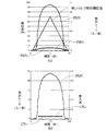
- FIG. 3A shows measured values V a1 of the first release rate sensor 4a and measured values of the second release rate sensor 4b when only the first deposition source 3a is heated using the deposited film manufacturing apparatus 1 of FIG. It is a graph showing the change of Vb1 .
- the heating temperature of the first vapor deposition source 3a is constant (320 ° C.), but the opening degree of the container 32a is changed from 0% to 30% over 4% intervals every 1.5%. After changing to 30% to 0%, it was changed over time at intervals of 4 seconds every 1.5%.
- the opening degree of the container 32a was adjusted using a shutter. An opening degree of 0% means that the opening 321a of the container 32a is completely blocked by the shutter.
- Tris (8-quinolinolato) aluminum (abbreviation: Alq 3 ) was used as the first organic vapor deposition material 31a included in the first vapor deposition source 3a, and the degree of vacuum in the chamber was 4 ⁇ 10 ⁇ 4 Pa. It was. From the result of FIG. 3A, it can be seen that the amount of the first organic vapor deposition material 31a released into the chamber 2 (V a1 and V b1 ) increases in proportion to the degree of opening of the container 32a.
- FIG. 3B shows the mixing rate (CR 21 ) of the first organic vapor deposition material 31a with respect to the second release rate sensor 4b based on the result of FIG. 3A and the above formula (1). It is the graph calculated according to the change. It should be noted that the first organic vapor deposition material 31a was released in such a small amount that it could hardly be detected by the second release rate sensor 4b between the apertures of 0% to 19.5% and 19.5% to 0%. The mixing rate (CR 21 ) in is not calculated. From this result, it is understood that the mixing rate (CR 21 ) always shows a substantially constant value (about 0.31) regardless of the opening degree of the container 32a. That is, the mixing rate (CR 21 ) is always substantially constant regardless of the discharge amount of the first organic vapor deposition material 31a.
- FIG. 4A shows the measured value V a2 of the first release rate sensor 4a and the measured value of the second release rate sensor 4b when only the second deposition source 3b is heated using the deposited film manufacturing apparatus 1 of FIG. It is a graph showing the change of Vb2 .
- the heating temperature of the second vapor deposition source 3b is constant (290 ° C.), but the opening degree of the container 32b is changed from 0% to 20% over a period of 4 seconds every 1.0%. After that, it was changed over time at intervals of 4 seconds every 1.0% from 20% to 0% again. The opening degree of the container 32b was adjusted using a shutter.
- the second organic vapor deposition material 31b included in the second vapor deposition source 3b bis (2-phenylquinolinato-N, C2 ′) iridium (III) acetylacetonate (abbreviation: Ir (pq) 2 (acac))
- the degree of vacuum in the chamber was 4 ⁇ 10 ⁇ 4 Pa. From the result of FIG. 4A, it can be seen that the amount (V a2 and V b2 ) of the second organic vapor deposition material 31b released into the chamber 2 increases in proportion to the opening degree of the container 32b.
- FIG. 4B shows the mixing rate (CR 12 ) of the second organic vapor deposition material 31b with respect to the first release rate sensor 4a based on the result of FIG. 4A and the above formula (1). It is the graph calculated according to the change.
- the mixing rate (CR 12 ) is not calculated. From this result, it is understood that the mixing rate (CR 12 ) always shows a substantially constant value (about 0.21) regardless of the opening degree of the container 32b. That is, the mixing rate (CR 12 ) is always substantially constant regardless of the amount of the second organic vapor deposition material 31b released.
- FIG. 5A shows measured values V a3 and second values of the first release rate sensor 4a when both the first vapor deposition source 3a and the second vapor deposition source 3b are heated using the vapor deposition film manufacturing apparatus 1 of FIG. It is a graph showing change of measured value Vb3 of discharge rate sensor 4b.
- the heating temperature of the first vapor deposition source 3a and the opening degree of the container 32a are the same as the conditions of FIG. 3A, and the heating temperature of the second vapor deposition source 3b and the opening degree of the container 32b are as shown in FIG. Same as condition.
- FIG. 5A shows measured values V a3 and second values of the first release rate sensor 4a when both the first vapor deposition source 3a and the second vapor deposition source 3b are heated using the vapor deposition film manufacturing apparatus 1 of FIG. It is a graph showing change of measured value Vb3 of discharge rate sensor 4b.
- the heating temperature of the first vapor deposition source 3a and the opening degree of the container 32a are the same
- V a1 a measured value of the first release rate sensor 4a and a measured value of the second release rate sensor 4b (only the first vapor deposition source 3a shown in FIG. 3A).
- V b1 and the measured value (V a2 ) of the first release rate sensor 4a and the measured value (V b2 ) of the second release rate sensor 4b when only the second vapor deposition source 3b shown in FIG. 4 (a) is heated.
- the vaporized j-th organic vapor deposition material is mixed in each emission rate sensor without being affected by the other vaporized organic vapor deposition materials in the chamber. Therefore, the mixing rate (CR ij ) of the j-th organic vapor deposition material with respect to the i-th emission rate sensor is the same even when each vapor deposition source is individually heated or when all vapor deposition sources are heated simultaneously. Value.
- the reason why the vaporized j-th organic vapor deposition material is not affected by other vaporized organic vapor deposition materials is not clear, but the present inventors presume as follows.
- the higher the degree of vacuum in the chamber the longer the mean free path of the vaporized organic vapor deposition material. Therefore, in the co-evaporation method using the organic vapor deposition material, the molecules in the jth organic vapor deposition material are less likely to collide with the molecules of the other organic vapor deposition material by setting the inside of the chamber to a vacuum state. As a result, the vaporized organic vapor deposition materials are mixed into the emission rate sensors without interfering with each other.
- the mean free path of the vapor deposition material becomes longer as the degree of vacuum is higher, and shorter as the molecular weight of the vapor deposition material is larger.
- the upper limit value of the degree of vacuum in the chamber is preferably 10 ⁇ 3 Pa, more preferably 10 ⁇ 4 Pa.
- the vapor deposition step is a step of forming an organic vapor deposition film on the surface of the substrate introduced into the vacuum chamber by simultaneously discharging all organic vapor deposition materials into the chamber.
- a vapor deposition process has a 1st vapor deposition process, a 2nd vapor deposition process, and a 3rd vapor deposition process in this order.
- the base material introduced into the chamber is not particularly limited, and can be appropriately changed according to the use of the organic vapor deposition film.
- the substrate include a glass plate, a ceramic plate, and a synthetic resin film.
- an organic vapor deposition film as a light emitting layer of an organic electroluminescent device, for example, based on a laminate having an electrode (cathode or anode), a hole (or electron) transport layer, and a hole (or electron) injection layer. It can be used as a material. In this case, a light emitting layer which is an organic vapor deposition film is formed on the surface of the hole (or electron) transport layer.
- the first vapor deposition step is a step of heating all (n) vapor deposition sources and detecting a measurement value (MV i ) of each emission rate sensor corresponding to each vapor deposition source. Since there are n emission rate sensors, n measurement values (MV i ) of the emission rate sensor are also detected.
- the mixing ratio of all the organic vapor deposition materials with respect to all the release rate sensors calculated in the third previous step, and the measured value (MV i ) of each emission rate sensor measured in the first vapor deposition step are used.
- the true emission rate (X j ) of each organic vapor deposition material is calculated based on the following formula (2).
- MV i is a measured value of the i-th release rate sensor when all the vapor deposition sources are heated in the first vapor deposition step.
- the measured value of the i-th release rate sensor is the release rate of the organic vapor deposition material including the i-th organic vapor deposition material and other organic vapor deposition materials mixed in the i-th release rate sensor.
- CR ij is a mixing rate of the j-th organic vapor deposition material with respect to the i-th release rate sensor.
- Equation (2) By substituting the measured value (MV i ) of the i-th release rate sensor and the mixing rate (CR ij ) of the j-th organic vapor deposition material with respect to the i-th release rate sensor into Equation (2), the true value of the j-th organic vapor deposition material is obtained.
- the release rate (X j ) is calculated.
- the measurement value (MV 1 ) of the first release rate sensor 4a measured in the second vapor deposition step is assumed to be 22 ⁇ / second, and the measurement value (MV 2 ) of the first release rate sensor 4a is 18 ⁇ / second.
- a binary simultaneous equation of the following equation (3) is derived.
- the true emission rate (X 1 ) of the first organic vapor deposition material 31a is 18 ⁇ / sec
- the true emission rate (X 2 ) of the second organic vapor deposition material 31b. ) Is 16 ⁇ / sec. That is, the measured value (MV 1 ) of the first release rate sensor 4a and the true release rate (X 1 ) of the first organic vapor deposition material 31a have an error of 4 ⁇ / second, and the measured value of the second release rate sensor 4b.
- the true emission rate (X 2 ) of (MV 2 ) and the second organic vapor deposition material 31b has an error of 2 ⁇ / sec.
- the true emission rate (X j ) of each organic vapor deposition material can be calculated by solving the n-ary simultaneous equations corresponding to the number (n) of vapor deposition sources.
- each organic vapor deposition material is calculated so that the deviation between the true release rate (X j ) of each organic vapor deposition material calculated in the second vapor deposition process and the target release rate (TR j ) of each organic vapor deposition material is small.
- This is a step of feedback control of the release condition of the vapor deposition material.
- the target release rate (TR j ) can be arbitrarily set according to the use of the deposited film.
- the release conditions of each organic vapor deposition material so that both rates coincide with each other. are changed sequentially.
- the absolute value of the deviation between the true release rate (X j ) and the target release rate (TR j ) of each organic vapor deposition material is preferably within 5% of the target release rate, more preferably within 3%. Particularly preferably, it is within 2%.
- the change of the release condition is not particularly limited as long as the measurement value (MV i ) of each release rate sensor fluctuates, and examples thereof include a change in the heating temperature of each vapor deposition source and the opening degree of the container.
- the true release rate (X j ) of the jth organic vapor deposition material is lower than its target release rate (TR j )
- the heating temperature of the jth organic vapor deposition source and the opening degree of the container are increased
- the true release rate (X j ) of the organic vapor deposition material is higher than its target release rate (TR j )
- the release conditions are changed so as to lower the heating temperature of the jth vapor deposition source and the opening degree of the container.
- each organic vapor deposition material By changing the emission condition, the measured value (MV i ) of each emission rate sensor changes, and the true emission rate (X j ) of each organic vapor deposition material also changes accordingly.
- feedback control is performed so that the true release rate (X j ) of each organic vapor deposition material matches the target release rate (TR j ).
- each organic vapor deposition material can be finally released into the chamber at a target release rate (TR j ).
- FIG. 6 is a flowchart of the vapor deposition process.
- “heating of all deposition sources” and “detection of release rate (MV i )” correspond to the first deposition step
- “calculation of true release rate (X j )” is the second deposition step.
- the subsequent steps correspond to the third vapor deposition step.
- the condition whether or not to end the vapor deposition step is not particularly limited, and can be arbitrarily set according to the function and application of the organic vapor deposition film to be formed.
- the deposition process can be set to end several seconds after the true release rate (X j ) matches the target release rate (TR j ).
- the vapor deposition process can be set to end when the fed base material is exhausted.
- transduces a base material in a chamber is not specifically limited.
- the base material may be introduced during the previous process (during the first pre-process to the third pre-process) or during the vapor deposition process (during the first vapor deposition process to the third vapor deposition process), and may be introduced before the previous process. Also good.
- the substrate is introduced into the chamber during the third deposition step. This is because the amount of each organic vapor deposition material adhering to the substrate becomes uneven because the release conditions of each organic vapor deposition material are not feedback controlled before the third vapor deposition step.
- the substrate is introduced into the chamber during the third vapor deposition step, if the vapor deposition film manufacturing apparatus 1 as shown in FIG.
- the vapor deposition area 21 of the second roll B is used until just before the substrate 5 is introduced. It is preferable that the exposed surface is covered with a cover member (not shown). This is because if the organic vapor deposition material adheres to the surface of the second roll B before introducing the base material 5 into the chamber 2, there is a possibility that proper feeding of the base material 5 may be hindered.
- the base material 5 is introduced into the chamber before the third vapor deposition step, as in the case where the base material is introduced into the chamber during the third vapor deposition step, the second time until just before the base material 5 is introduced.
- the surface of the roll B may be covered with a cover member, but the substrate 5 itself can also be used as a cover member.
- the organic vapor deposition material can be prevented from adhering to the surface of the second roll B by covering the surface of the second roll B with the base material 5 introduced into the chamber.
- the base material 5 itself is used as a cover member, it is preferable that the base material 5 is not sent out in the chamber until the release conditions of each organic vapor deposition material are feedback controlled in the third vapor deposition step.
- the organic vapor deposition material adheres only to a part of the base material 5 exposed in the vapor deposition area 21, and the area of the base material 5 used as a cover member can be minimized. it can.
- a part of the base material 5 used as the cover member is attached with an organic vapor deposition material having a vapor deposition amount that does not reflect the target release rate. Therefore, a part of the base material 5 used as the cover member is usually discarded after the organic vapor deposition film is formed on the whole base material 5.
- each organic vapor deposition material can be released into the chamber at a desired release rate (target release rate).
- target release rate target release rate
- an organic vapor deposition film containing each organic vapor deposition material in a desired ratio can be formed.
- the organic vapor deposition film formed by this invention can be used as a light emitting layer of an organic electroluminescent apparatus. Since this light emitting layer contains each organic vapor deposition material in a desired ratio, it has an excellent light emitting function.
- a vapor deposition film manufacturing apparatus having two vapor deposition sources was used, but the vapor deposition film manufacturing apparatus used in the present invention was used in the first embodiment. It is not limited to things.
- the vapor deposition film manufacturing apparatus used in 2nd Embodiment of this invention is demonstrated, it mainly refers only about a different part from the vapor deposition film manufacturing apparatus of 1st Embodiment.
- FIG. 7 is a schematic diagram showing a vapor deposition film manufacturing apparatus 1 used in the second embodiment of the present invention.
- the chamber 2 has a mixing chamber 6 having a discharge port 61 therein.
- the mixing chamber 6 is a chamber provided for mixing n kinds of organic vapor deposition materials 31 included in the n vapor deposition sources 3.
- the containers 32 of the n vapor deposition sources 3 are connected to the mixing chamber 6. It communicates via a cylindrical member 7.
- each deposition source 3 is provided outside the chamber 2, but each deposition source 3 may be provided inside the chamber 2 (not shown).
- the number of vapor deposition sources 3 is three (the first vapor deposition source 3a to the third vapor deposition source 3c), but the number of vapor deposition sources 3 may be two or four or more. May be.
- the cylindrical member 7 has a hollow portion 71 through which the vapor-deposited organic vapor deposition material can pass, and further has a valve portion 72 that can arbitrarily change the width of the hollow portion 71.
- the structure of the valve portion 72 is not particularly limited. For example, as shown in FIG. 7, a plug portion 721 that penetrates from the outer peripheral surface of the tubular member to the cavity portion, and an end portion of the plug portion 721 (the outer side of the cavity portion 71) And a bar portion 722 provided on a portion exposed to the surface.
- each organic vapor deposition material 31 flowing into the mixing chamber is adjusted. can do.
- fine holes pin holes
- each release rate sensor is located in the vicinity of the fine holes. 4 is provided.
- Each release rate sensor 4 measures the release rate of each organic vapor deposition material 31 based on each organic vapor deposition material 31 leaking from the fine holes.
- Each release rate sensor 4 may be provided inside the mixing chamber 6 and in the vicinity of the end of the cylindrical member 7 (not shown). In the present invention, the true emission rate of each organic vapor deposition material 31 can be calculated regardless of the position of the emission rate sensor 4.
- each organic vapor deposition material 31 that has flowed from each vapor deposition source 3 into each mixing chamber 6 through each cylindrical member 7 is mixed in the mixing chamber 6. Thereafter, the mixed organic vapor deposition material 31 is discharged from the discharge port 61 and adheres to the surface of the substrate 5.
- the distance D between the discharge port 61 and the surface of the substrate 5 is not particularly limited, but is preferably 10 mm or less, more preferably 5 mm or less, and particularly preferably 1 mm or less. Further, the lower limit value of the distance D is not particularly limited, but actually, it is 0.5 mm or more. The shorter the distance D, the faster the vapor deposition film can be formed on the surface of the substrate 5.
- the vapor deposition film manufacturing method of the present invention since the vapor deposition film manufacturing method of the present invention is used, the true release rate X j of each organic vapor deposition material 31 substantially matches the target release rate TR j , so that each organic vapor deposition material 31 is included at a desired ratio.
- the deposited film can be formed with high accuracy.
- the vapor deposition film manufacturing apparatus (refer FIG. 7) which has the mixing chamber used in 2nd Embodiment of this invention was prepared.
- the number of vapor deposition sources was three.
- the degree of vacuum in the chamber was set to 4 ⁇ 10 ⁇ 4 Pa.
- Alq 3 was used as the first organic vapor deposition material included in the first vapor deposition source.
- Ir (pq) 2 (acac) was used as the second organic vapor deposition material contained in the second vapor deposition source.
- N, N′-bis (naphthalen-1-yl) -N, N′-bis (phenyl) -2,2′-dimethylbenzidine (abbreviation: ⁇ - NPD) was used.
- ⁇ - NPD N, N′-bis (naphthalen-1-yl) -N, N′-bis (phenyl) -2,2′-dimethylbenzidine
- the degree of opening described below is based on the width (100%) of the cavity when the valve part is not pushed in, and the degree of opening is adjusted by pushing or pulling out the valve.
- the valve portion corresponding to the nth vapor deposition source is referred to as an nth valve portion.
- FIG. 8A is a graph in which measured values (PMV 1 to PMV 3 ) of the first release rate sensor to the third release rate sensor in the meantime are plotted over time
- FIG. 2 is a graph plotted over time the value of the mixing ratio of the first organic vapor deposition material on the release rate sensor (CR 21), and a third mixing ratio of the first organic vapor deposition material on the release rate sensor (CR 31).
- CR 21 was substantially constant at 0.050, and CR 31 was substantially constant at 0.056.
- the amount of the first organic vapor deposition material mixed in the second and third release rate sensors is extremely small between 0% to 15% and 15% to 0, the CR 21 and CR 31 are calculated. I didn't.
- FIG. 9A is a graph in which measured values (PMV 1 to PMV 3 ) of the first release rate sensor to the third release rate sensor in the meantime are plotted over time
- FIG. 1 is a over time graph plotting the values of contamination of the second organic evaporation material on the release rate sensor (CR 12), and a third mixing ratio of the second organic evaporation material on the release rate sensor (CR 32).
- CR 12 was substantially constant at 0.280, and CR 32 was substantially constant at 0.242.
- the amount of the second organic vapor deposition material mixed in the first and third emission rate sensors is extremely small between 0% to 20% and 20% to 0, the CR 12 and CR 32 are calculated. I didn't.
- FIG. 10A is a graph in which measured values (PMV 1 to PMV 3 ) of the first release rate sensor to the third release rate sensor in the meantime are plotted over time
- FIG. 1 is a over time graph plotting the value of mixing ratio of the third organic vapor deposition material on the release rate sensor (CR 13) and mixing ratio of the third organic evaporation material for the second discharge rate sensor (CR 23).
- CR 13 was substantially constant at 0.067, and CR 23 was substantially constant at 0.053. Since the amount of the third organic vapor deposition material mixed in the first and second emission rate sensors is extremely small between 0% to 15% and 15% to 0%, the CR 13 and CR 23 are calculated. I didn't.
- FIG. 11B shows the target release rate (TR 1 ) of the first to third organic vapor deposition materials, except for the measurement values (MV 1 to MV 3 ) of the first to third release rate sensors from FIG. ⁇ TR 3 ) are represented by broken lines.
- the opening degree of the first to third valve portions and the heating temperature of the first to third evaporation sources were changed. From the result of FIG. 11B, it can be read that the true release rate (X 1 to 3 ) substantially matches the target release rate (TR 1 to 3 ) of each organic vapor deposition material after about 100 seconds.
Landscapes
- Chemical & Material Sciences (AREA)
- Engineering & Computer Science (AREA)
- Chemical Kinetics & Catalysis (AREA)
- Materials Engineering (AREA)
- Mechanical Engineering (AREA)
- Metallurgy (AREA)
- Organic Chemistry (AREA)
- Manufacturing & Machinery (AREA)
- Electroluminescent Light Sources (AREA)
- Physical Vapour Deposition (AREA)
Abstract
【課題】 基材に対する各有機蒸着材料の蒸着量を正確に制御できる有機蒸着膜の製造方法を提供する。 【解決手段】 本発明は、内部を真空状態に保持したチャンバー2と、前記チャンバー2内に放出する有機蒸着材料31を含むn個の蒸着源3と、前記n個の蒸着源3に対応して前記有機蒸着材料3の放出レートを測定するn個の放出レートセンサ4と、を有する蒸着膜製造装置1を準備する準備工程と、前記蒸着膜製造装置1を用いて各放出レートセンサ4に対する各有機蒸着材料31の混入率を算出する前工程と、全ての有機蒸着材料31を同時に前記チャンバー2内に放出することにより前記チャンバー2内に導入した基材5の表面に有機蒸着膜を形成する蒸着工程と、を有する。
Description
本発明は、有機蒸着膜の製造方法、及び前記製造方法によって形成された有機蒸着膜を有する有機エレクトロルミネッセンス装置に関する。
従来、蒸着法によって蒸着膜を形成することが知られている。一般的に、蒸着法とは、蒸着源に含まれる蒸着材料(例えば、金属酸化物や有機化合物)を加熱し気化させ、この気化させた蒸着材料を基材の表面に付着させることにより、基材の表面に蒸着材料の薄膜(蒸着膜)を形成する方法を指す。
蒸着法の一つとして、共蒸着法が知られている。共蒸着法は、真空チャンバー内に設けられた2個以上の蒸着源に含まれる異なった蒸着材料を同時に加熱することにより、2種以上の蒸着材料を含んだ蒸着膜を基材の表面に形成する方法である。
共蒸着法は、様々な技術分野で用いられている。例えば、有機化合物を含む蒸着材料(有機蒸着材料)であるホスト材料とドーパント材料を共蒸着することで有機蒸着膜を形成し、この有機蒸着膜を発光層として用いた有機エレクトロルミネッセンス装置が知られている(特許文献1)。
蒸着法の一つとして、共蒸着法が知られている。共蒸着法は、真空チャンバー内に設けられた2個以上の蒸着源に含まれる異なった蒸着材料を同時に加熱することにより、2種以上の蒸着材料を含んだ蒸着膜を基材の表面に形成する方法である。
共蒸着法は、様々な技術分野で用いられている。例えば、有機化合物を含む蒸着材料(有機蒸着材料)であるホスト材料とドーパント材料を共蒸着することで有機蒸着膜を形成し、この有機蒸着膜を発光層として用いた有機エレクトロルミネッセンス装置が知られている(特許文献1)。
共蒸着法を用いる場合、通常、チャンバー内には、各蒸着源に対応する放出レートセンサが設けられており、この放出レートセンサの測定値に基づいて各蒸着材料の蒸着量が推定される。
しかし、放出レートセンサの値に基づいて各蒸着材料の蒸着量を推定しても、所望量の各蒸着材料を基材の表面に正確に蒸着させることは困難であり、この問題は、有機蒸着材料を用いる場合に特に顕著である。
所望量の各有機蒸着材料を正確に蒸着できない場合、得られた有機蒸着膜に含まれる各有機蒸着材料の比率は当然ながら所望の値とならない。その結果、得られた有機蒸着膜の機能性が低下するという問題がある。
例えば、上記発光層において、ホスト材料とドーパント材料が所望の比率で含まれていない場合、有機エレクトロルミネッセンス装置の発光機能が低下し、色むらなどが発生する一因となる。
しかし、放出レートセンサの値に基づいて各蒸着材料の蒸着量を推定しても、所望量の各蒸着材料を基材の表面に正確に蒸着させることは困難であり、この問題は、有機蒸着材料を用いる場合に特に顕著である。
所望量の各有機蒸着材料を正確に蒸着できない場合、得られた有機蒸着膜に含まれる各有機蒸着材料の比率は当然ながら所望の値とならない。その結果、得られた有機蒸着膜の機能性が低下するという問題がある。
例えば、上記発光層において、ホスト材料とドーパント材料が所望の比率で含まれていない場合、有機エレクトロルミネッセンス装置の発光機能が低下し、色むらなどが発生する一因となる。
本発明の目的は、各有機蒸着材料の蒸着量を正確に制御できる有機蒸着膜の製造方法、及び発光機能に優れた有機蒸着膜を発光層として有する有機エレクトロルミネッセンス装置を提供することである。
本発明者らは、共蒸着法において、所望量の各有機蒸着材料を正確に蒸着し難い一因は、気化した有機蒸着材料の一部が各蒸着源に対応して設けられた放出レートセンサの測定値に影響するためであることを発見した。
以下、図1を参照しつつ具体的に説明する。なお、本発明では、複数の蒸着源や放出レートセンサを用いる。そのため、本明細書では各蒸着源や各放出レートセンサを区別するため、それらの符号に「a」や「b」などの小文字のアルファベットを付記する場合がある。
以下、図1を参照しつつ具体的に説明する。なお、本発明では、複数の蒸着源や放出レートセンサを用いる。そのため、本明細書では各蒸着源や各放出レートセンサを区別するため、それらの符号に「a」や「b」などの小文字のアルファベットを付記する場合がある。
図1は、一般的な蒸着膜製造装置1の概要図である。蒸着膜製造装置1のチャンバー2内には、有機蒸着材料31を含む蒸着源3が設けられている。図1において、矢印は、真空状態のチャンバー2内における有機蒸着材料31の流路を示し、矢印の太さは、有機蒸着材料31の流量を反映している。白矢印は、後述する第1有機蒸着材料31aの流路及び流量を表し、黒矢印は、後述する第2有機蒸着材料31bの流路及び流量を表す。
図1では、真空チャンバー2内に、2個の蒸着源3(第1蒸着源3a及び第2蒸着源3b)が設けられている。第1蒸着源3aは、第1有機蒸着材料31aを含んでおり、第2蒸着源3bは、第2有機蒸着材料31bを含んでいる。チャンバー2内には、第1有機蒸着材料31aがチャンバー2内に放出される速度(放出レート)を測定する第1放出レートセンサ4aが第1蒸着源3aに対応して設けられていると共に、第2有機蒸着材料31bの放出レートを測定する第2放出レートセンサ4bが第2蒸着源3bに対応して設けられている。また、第1及び第2蒸着源3a,3bの間には、第1有機蒸着材料31a又は第2有機蒸着材料31bが第2放出レートセンサ4b又は第1放出レートセンサ4aに混入しないように隔壁23が設けられている。
図1では、真空チャンバー2内に、2個の蒸着源3(第1蒸着源3a及び第2蒸着源3b)が設けられている。第1蒸着源3aは、第1有機蒸着材料31aを含んでおり、第2蒸着源3bは、第2有機蒸着材料31bを含んでいる。チャンバー2内には、第1有機蒸着材料31aがチャンバー2内に放出される速度(放出レート)を測定する第1放出レートセンサ4aが第1蒸着源3aに対応して設けられていると共に、第2有機蒸着材料31bの放出レートを測定する第2放出レートセンサ4bが第2蒸着源3bに対応して設けられている。また、第1及び第2蒸着源3a,3bの間には、第1有機蒸着材料31a又は第2有機蒸着材料31bが第2放出レートセンサ4b又は第1放出レートセンサ4aに混入しないように隔壁23が設けられている。
真空状態にしたチャンバー2内で、第1及び第2蒸着源3a,3bを同時に加熱することにより、気化した第1及び第2有機蒸着材料31a,31bが蒸着対象である基材5に向かって放出される(各太矢印参照)。
しかしながら、隔壁23を設けたとしても、チャンバー2内において第1及び第2有機蒸着材料31a,31bは気化しているため、第1有機蒸着材料31aの一部は、隔壁23を超えて第2蒸着源3b側に回り込み、同様に、第2有機蒸着材料31bの一部は、隔壁23を超えて第1蒸着源3a側に回り込む(各細矢印参照)。そのため、混入を完全に防止することはできない。そして、隔壁23を超えて回り込んだ第1有機蒸着材料31aの一部又は第2有機蒸着材料31bの一部は、第2蒸着源3b又は第1蒸着源3aに対応する第2放出レートセンサ4b又は第1放出レートセンサ4aに付着するため、各放出レートセンサ4a,4bの測定値は、各有機蒸着材料31a,31bの真の放出レートを反映しなくなる。
しかしながら、隔壁23を設けたとしても、チャンバー2内において第1及び第2有機蒸着材料31a,31bは気化しているため、第1有機蒸着材料31aの一部は、隔壁23を超えて第2蒸着源3b側に回り込み、同様に、第2有機蒸着材料31bの一部は、隔壁23を超えて第1蒸着源3a側に回り込む(各細矢印参照)。そのため、混入を完全に防止することはできない。そして、隔壁23を超えて回り込んだ第1有機蒸着材料31aの一部又は第2有機蒸着材料31bの一部は、第2蒸着源3b又は第1蒸着源3aに対応する第2放出レートセンサ4b又は第1放出レートセンサ4aに付着するため、各放出レートセンサ4a,4bの測定値は、各有機蒸着材料31a,31bの真の放出レートを反映しなくなる。
従って、各有機蒸着材料31a,31bを所望の放出レートで蒸着しようとしても、各放出レートセンサ4a,4bの測定値は各有機蒸着材料31a,31bの真の放出レートを反映していないため、各有機蒸着材料31a,31bの基材5に対する蒸着量を制御することが困難となる。
本発明者らは、このように、気化した各有機蒸着材料が、それに対応する放出レートセンサの測定値だけでなく、チャンバー内に存在する全ての放出レートセンサの測定値に影響することを発見した。さらに、本発明者らは、鋭意研究を行った結果、各放出レートセンサに対する各有機蒸着材料の混入率は、各有機蒸着材料の放出量に関わらず略一定であり、且つ、全ての蒸着源を同時に加熱しても前記混入率は略一定であるという法則性を見出し、本発明を完成させた。
本発明者らは、このように、気化した各有機蒸着材料が、それに対応する放出レートセンサの測定値だけでなく、チャンバー内に存在する全ての放出レートセンサの測定値に影響することを発見した。さらに、本発明者らは、鋭意研究を行った結果、各放出レートセンサに対する各有機蒸着材料の混入率は、各有機蒸着材料の放出量に関わらず略一定であり、且つ、全ての蒸着源を同時に加熱しても前記混入率は略一定であるという法則性を見出し、本発明を完成させた。
本発明の有機蒸着膜の製造方法は、内部を真空状態に保持したチャンバーと、前記チャンバー内に放出する有機蒸着材料を含むn個の蒸着源と、前記n個の蒸着源に対応して前記有機蒸着材料の放出レートを測定するn個の放出レートセンサと、を有する蒸着膜製造装置を準備する準備工程と、前記蒸着膜製造装置を用いて、各放出レートセンサに対する各有機蒸着材料の混入率を算出する前工程と、全ての有機蒸着材料を同時に前記チャンバー内に放出することにより、前記チャンバー内に導入した基材の表面に有機蒸着膜を形成する蒸着工程と、を有し、前記前工程が、前記n個の蒸着源から選択した1個の第j蒸着源のみを加熱し、前記第j蒸着源に含まれる第j有機蒸着材料を前記チャンバー内に放出する第1前工程と、前記第1前工程で加熱した前記第j蒸着源に対応する第j放出レートセンサの測定値(PMVj)及び第i蒸着源に対応する第i放出レートセンサの測定値(PMVi)に基づき、下記式(1)で表される前記第i放出レートセンサに対する前記第j有機蒸着材料の混入率(CRij)を全ての放出レートセンサについて算出する第2前工程と、前記第j蒸着源を変更し、前記第1及び第2前工程と同じ工程を繰り返すことにより、全ての放出レートセンサに対する各有機蒸着材料の混入率を全ての有機蒸着材料について算出する第3前工程と、を有し、

前記蒸着工程が、全ての蒸着源を加熱し、各蒸着源に対応する各放出レートセンサの測定値(MVi)を検出する第1蒸着工程と、前記第3前工程で算出した全ての放出レートセンサに対する全ての有機蒸着材料の混入率、及び、前記第1蒸着工程で検出した各放出レートセンサの測定値を用いて、下記式(2)に基づき、各有機蒸着材料の真の放出レート(Xj)を算出する第2蒸着工程と、前記第2蒸着工程で算出した各有機蒸着材料の真の放出レート(Xj)と各有機蒸着材料の目標放出レート(TRj)との偏差が小さくなるように、各有機蒸着材料の放出条件をフィードバック制御する第3蒸着工程と、を有する。

好ましくは、本発明の有機蒸着膜の製造方法は、前記n個の蒸着源のそれぞれが、有機蒸着材料を収容した収容器を有しており、前記チャンバーが、その内側に、放出口を有する混合室を有しており、前記n個の蒸着源の各収容器が、前記混合室に連通されており、前記蒸着工程において、前記n個の蒸着源に含まれる各有機蒸着材料を前記混合室で混合し、且つ、前記混合した有機蒸着材料を前記放出口から基材の表面に向かって放出する。
好ましくは、本発明の有機蒸着膜の製造方法は、前記n個の蒸着源の各収容器が、気化した有機蒸着材料が通り抜け可能な空洞部を有する筒状部材を介して前記混合室に連通されており、前記筒状部材が、前記空洞部の幅を任意に変更可能なバルブ部を有する。
好ましくは、本発明の有機蒸着膜の製造方法は、前記第3蒸着工程において、各蒸着源の加熱温度を変更することにより、各有機蒸着材料の放出条件をフィードバック制御する。また、好ましくは、本発明の有機蒸着膜の製造方法は、前記第3蒸着工程において、前記バルブ部を用いて前記空洞部の幅を変更することにより、各有機蒸着材料の放出条件をフィードバック制御する。
好ましくは、本発明の有機蒸着膜の製造方法は、前記蒸着工程において、前記混合室の放出口と前記基材の距離が10mm以下である。
好ましくは、本発明の有機蒸着膜の製造方法は、前記チャンバー内の真空度が10-3Pa以下である。
本発明の別の局面によれば、有機エレクトロルミネッセンス装置を提供する。本発明の有機エレクトロルミネッセンス装置は、上記の有機蒸着膜の製造方法によって形成された有機蒸着膜を発光層として有する。
本発明の有機蒸着膜の製造方法は、各有機蒸着材料を所望の放出レートでチャンバー内に放出できるため、基材に対する各有機蒸着材料の蒸着量を正確に制御でき、その結果、各有機蒸着材料を所望の比率で含んだ有機蒸着膜を形成することができる。
また、本発明の有機エレクトロルミネッセンス装置は、各有機蒸着材料を所望の比率で含んだ有機蒸着膜を発光層として有するため、発光機能に優れる。
また、本発明の有機エレクトロルミネッセンス装置は、各有機蒸着材料を所望の比率で含んだ有機蒸着膜を発光層として有するため、発光機能に優れる。
本発明の有機蒸着膜の製造方法は、準備工程と、前工程と、蒸着工程と、を有する。準備工程は、蒸着膜製造装置を準備する工程であり、前工程は、各放出レートセンサに対する各有機蒸着材料の混入率を算出する工程であり、蒸着工程は、基材の表面に有機蒸着材料を共蒸着する工程である。本発明では、準備工程、前工程、及び蒸着工程はこの順に行われる。
以下、各工程について説明する。
以下、各工程について説明する。
<準備工程>
準備工程は、蒸着膜製造装置を準備する工程である。
蒸着膜製造装置は、内部を真空状態に保持したチャンバーと、チャンバー内に放出する有機蒸着材料を含むn個の蒸着源と、n個の蒸着源に対応して有機蒸着材料の放出レートを測定するn個の放出レートセンサと、を有する。n個の蒸着源の各々は、それぞれ異なる有機蒸着材料を含んでいる。
nは、2以上の自然数であり、nの値は、共蒸着する有機蒸着材料の種類数に合わせて適宜変更することができる。本発明では、n個の蒸着源の各々がそれぞれ異なる種類の有機蒸着材料を含んでいるため、n種類の有機蒸着材料が用いられる。
以下、本発明について、図2に示す本発明の第1実施形態に係る蒸着膜製造装置を例にして説明する。
なお、図2の蒸着膜製造装置1は、2個の蒸着源3a,3bを有する(即ち、2種類の有機蒸着材料31a,31bを用いている)が、本発明では蒸着源3の数は2個に限定されない。また、チャンバー2や蒸着源3の構造も本実施形態に限定されない。
準備工程は、蒸着膜製造装置を準備する工程である。
蒸着膜製造装置は、内部を真空状態に保持したチャンバーと、チャンバー内に放出する有機蒸着材料を含むn個の蒸着源と、n個の蒸着源に対応して有機蒸着材料の放出レートを測定するn個の放出レートセンサと、を有する。n個の蒸着源の各々は、それぞれ異なる有機蒸着材料を含んでいる。
nは、2以上の自然数であり、nの値は、共蒸着する有機蒸着材料の種類数に合わせて適宜変更することができる。本発明では、n個の蒸着源の各々がそれぞれ異なる種類の有機蒸着材料を含んでいるため、n種類の有機蒸着材料が用いられる。
以下、本発明について、図2に示す本発明の第1実施形態に係る蒸着膜製造装置を例にして説明する。
なお、図2の蒸着膜製造装置1は、2個の蒸着源3a,3bを有する(即ち、2種類の有機蒸着材料31a,31bを用いている)が、本発明では蒸着源3の数は2個に限定されない。また、チャンバー2や蒸着源3の構造も本実施形態に限定されない。
(チャンバー)
チャンバー2は、その内部を真空状態に保持できる筐体である。チャンバー2には、真空ポンプ(図示せず)が接続されており、この真空ポンプを用いてチャンバー2内部を減圧し、真空状態が保持される。
チャンバー2内の真空度の上限値は特に限定されないが、好ましくは10-3Pa(即ち、0.001Pa)であり、より好ましくは10-4Pa(即ち、0.0001Pa)である。また、真空度の下限値は特に限定されないが、現実的な観点から10-6Pa(即ち、0.000001Pa)であり、好ましくは10-5Pa(即ち、0.00001Pa)である。
真空度が高ければ高いほど、チャンバー2内に放出された各有機蒸着材料31a,31bの平均自由行程が長くなり、各有機蒸着材料31a,31bがチャンバー2内で干渉し難くなるため、蒸着工程において各有機蒸着材料31a,31bの真の放出レートを正確に算出することができる(具体的には、後述の前工程の欄にて説明する)。
チャンバー2は、その内部を真空状態に保持できる筐体である。チャンバー2には、真空ポンプ(図示せず)が接続されており、この真空ポンプを用いてチャンバー2内部を減圧し、真空状態が保持される。
チャンバー2内の真空度の上限値は特に限定されないが、好ましくは10-3Pa(即ち、0.001Pa)であり、より好ましくは10-4Pa(即ち、0.0001Pa)である。また、真空度の下限値は特に限定されないが、現実的な観点から10-6Pa(即ち、0.000001Pa)であり、好ましくは10-5Pa(即ち、0.00001Pa)である。
真空度が高ければ高いほど、チャンバー2内に放出された各有機蒸着材料31a,31bの平均自由行程が長くなり、各有機蒸着材料31a,31bがチャンバー2内で干渉し難くなるため、蒸着工程において各有機蒸着材料31a,31bの真の放出レートを正確に算出することができる(具体的には、後述の前工程の欄にて説明する)。
本実施形態において、チャンバー2の内部は、水平方向に架設された第1隔壁231によって、蒸着エリア21と非蒸着エリア22に区画されている。蒸着エリア21は、基材5に有機蒸着材料31a,31bを蒸着するエリアであり、蒸着工程において有機蒸着材料31a,31bによって満たされるエリアである。他方、非蒸着エリアは、基材5を蒸着しないエリアであり、蒸着工程において有機蒸着材料31a,31bが殆ど存在しないエリアである。第1隔壁231は、蒸着エリア21から非蒸着エリア22に連通する孔部を有しており、この孔部を介して基材5が非蒸着エリア21から蒸着エリア22に導入される。
また、本実施形態では、蒸着エリア21内には、各放出レートセンサ4a,4b間における各有機蒸着材料31a,31bの混入を防止するために、第2隔壁232が立設されている。
なお、第1隔壁231及び第2隔壁232は、必ずしも設けられていなくてもよい。もっとも、第2隔壁232が存在しない場合、各放出レートセンサ4a,4bに対する各有機蒸着材料31a,31bの混入量が多くなり、結果として蒸着工程における蒸着効率が低下する。そのため、各蒸着源3a,3b間には第2隔壁232が設けられることが好ましい。
また、本実施形態では、蒸着エリア21内には、各放出レートセンサ4a,4b間における各有機蒸着材料31a,31bの混入を防止するために、第2隔壁232が立設されている。
なお、第1隔壁231及び第2隔壁232は、必ずしも設けられていなくてもよい。もっとも、第2隔壁232が存在しない場合、各放出レートセンサ4a,4bに対する各有機蒸着材料31a,31bの混入量が多くなり、結果として蒸着工程における蒸着効率が低下する。そのため、各蒸着源3a,3b間には第2隔壁232が設けられることが好ましい。
本実施形態では、基材5は、長尺状であり、チャンバー2の外側にある第1ロールAに巻回されている。蒸着工程では、この巻回された基材5を繰り出し、順次チャンバー2内に導入することで基材5の表面に有機蒸着膜が形成される。具体的には、第1ロールAから繰り出された基材5は、チャンバー2内の非蒸着エリア22に導入され、その後、非蒸着エリア22と蒸着エリア21に第1隔壁231の孔部を介して跨がる第2ロールBによって蒸着エリア21に導入される。その後、再び、基材5は非蒸着エリア22に再び導入され、チャンバー2の外側にある第3ロールCに再び巻回される。基材5は、蒸着エリア21に露出している間だけ、有機蒸着材料31a,31bによって共蒸着される。図2において、矢印は、基材5の繰り出し方向を表す。
なお、図2では、基材5はチャンバー2内に導入されているが、準備工程及び後述する前工程の段階では、基材5はチャンバー2内に導入しなくてもよい。
なお、図2では、基材5はチャンバー2内に導入されているが、準備工程及び後述する前工程の段階では、基材5はチャンバー2内に導入しなくてもよい。
(蒸着源)
蒸着源3は、有機蒸着材料31と、有機蒸着材料31を収容した収容器32を有する。収容器32は、その上部にチャンバー2内に向かって開口した開口部321を有する。収容器32には、開口部321の開口度を調整するシャッターが設けられていてもよい(図示せず)。シャッターは、開口部321を覆うことにより、有機蒸着材料31の放出量を調整できる部材である。シャッターが開口部321を覆う面積は、任意に変更することができる。
収容器32は、耐熱性を有するものであれば特に限定されず、例えば、酸化アルミニウムや窒化ホウ素などからなる坩堝を用いることができる。収容器32を加熱すると、間接的に収容器に収容された有機蒸着材料31が加熱される。加熱された有機蒸着材料31は気化し、収容器32の開口部321を介してチャンバー2内に放出される。
なお、蒸着源3(収容器32)を加熱する方法は、特に限定されず、例えば、赤外線ランプや、タングステンやタンタルなどの金属ワイヤーを用いたワイヤーヒーターなどを用いた抵抗加熱方式などが用いられる。ワイヤーヒーターを用いる場合、収容器32の外周面に金属ワイヤーが巻き付けられる(図示せず)。
蒸着源3は、有機蒸着材料31と、有機蒸着材料31を収容した収容器32を有する。収容器32は、その上部にチャンバー2内に向かって開口した開口部321を有する。収容器32には、開口部321の開口度を調整するシャッターが設けられていてもよい(図示せず)。シャッターは、開口部321を覆うことにより、有機蒸着材料31の放出量を調整できる部材である。シャッターが開口部321を覆う面積は、任意に変更することができる。
収容器32は、耐熱性を有するものであれば特に限定されず、例えば、酸化アルミニウムや窒化ホウ素などからなる坩堝を用いることができる。収容器32を加熱すると、間接的に収容器に収容された有機蒸着材料31が加熱される。加熱された有機蒸着材料31は気化し、収容器32の開口部321を介してチャンバー2内に放出される。
なお、蒸着源3(収容器32)を加熱する方法は、特に限定されず、例えば、赤外線ランプや、タングステンやタンタルなどの金属ワイヤーを用いたワイヤーヒーターなどを用いた抵抗加熱方式などが用いられる。ワイヤーヒーターを用いる場合、収容器32の外周面に金属ワイヤーが巻き付けられる(図示せず)。
蒸着源3の数は、有機蒸着材料31の種類数と等しく、その数はn個である。図2では、2個の蒸着源3(即ち、第1蒸着源3a及び第2蒸着源3b)が用いられているため、この蒸着膜製造装置1によって形成される有機蒸着膜は、2種の有機蒸着材料31a,31bを含んでいる。
有機蒸着材料は、有機化合物を含んだ蒸着材料であり、好ましくは実質的に有機化合物のみからなる蒸着材料である。なお、「実質的に有機化合物のみからなる」とは、完全に有機化合物のみからなる場合だけでなく、本発明の効果を損なわない範囲で有機化合物以外の化合物が含まれている場合を含み、例えば、有機蒸着材料全体における有機化合物の割合が98質量%以上である場合を含む。
有機蒸着材料に含まれる有機化合物は特に限定されず、蒸着膜の用途に応じて適宜選択することができる。
なお、有機化合物とは、構造の基本骨格に炭素原子を有する化合物(但し、一酸化炭素、二酸化炭素、金属炭酸塩、青酸、金属青酸塩、金属シアン酸塩、金属チオシアン酸塩、その他の歴史的に無機化合物として扱われるものを除く)をいう。
なお、有機化合物とは、構造の基本骨格に炭素原子を有する化合物(但し、一酸化炭素、二酸化炭素、金属炭酸塩、青酸、金属青酸塩、金属シアン酸塩、金属チオシアン酸塩、その他の歴史的に無機化合物として扱われるものを除く)をいう。
例えば、有機蒸着膜を有機エレクトロルミネッセンス装置の発光層として用いる場合、ホスト材料やドーパント材料が有機蒸着材料として用いられる。
ホスト材料は、発光層中において主に電子や正孔の電荷輸送機能を有する化合物であり、ドーパント材料は、発光層中において主に発光機能を有する化合物である。
ホスト材料としては、例えば、1,3,5-トリ(9H-カルバゾール-9-イル)ベンゼン(略称:TCP)、1,3-ビス(カルバゾール-9-イル)ベンゼン(略称:mCP)、2,6-ビス(N-カルバゾリル)ピリジン、9,9-ジ(4-ジカルバゾール-ベンジル)フルオレン(略称:CPF)、4,4’-ビス(カルバゾール-9-イル)-9,9-ジメチル-フルオレン(略称:DMFL-CBP)などのカルバゾール誘導体などを用いることができる。
また、ドーパント材料としては、例えば、スチリル誘導体;ペリレン誘導体;トリス(2-フェニルピリジナト)イリジウム(III)(Ir(ppy)3)、トリス(1-フェニルイソキノリン)イリジウム(III)(Ir(piq)3)、ビス(1-フェニルイソキノリン)(アセチルアセトナト)イリジウム(III)(略称:Ir(piq)2(acac))などの有機イリジウム錯体などの燐光発光性金属錯体;などを用いることができる。
ホスト材料は、発光層中において主に電子や正孔の電荷輸送機能を有する化合物であり、ドーパント材料は、発光層中において主に発光機能を有する化合物である。
ホスト材料としては、例えば、1,3,5-トリ(9H-カルバゾール-9-イル)ベンゼン(略称:TCP)、1,3-ビス(カルバゾール-9-イル)ベンゼン(略称:mCP)、2,6-ビス(N-カルバゾリル)ピリジン、9,9-ジ(4-ジカルバゾール-ベンジル)フルオレン(略称:CPF)、4,4’-ビス(カルバゾール-9-イル)-9,9-ジメチル-フルオレン(略称:DMFL-CBP)などのカルバゾール誘導体などを用いることができる。
また、ドーパント材料としては、例えば、スチリル誘導体;ペリレン誘導体;トリス(2-フェニルピリジナト)イリジウム(III)(Ir(ppy)3)、トリス(1-フェニルイソキノリン)イリジウム(III)(Ir(piq)3)、ビス(1-フェニルイソキノリン)(アセチルアセトナト)イリジウム(III)(略称:Ir(piq)2(acac))などの有機イリジウム錯体などの燐光発光性金属錯体;などを用いることができる。
ホスト材料とドーパント材料を含む有機蒸着膜(発光層)を形成する場合、有機蒸着材料としてホスト材料を含む蒸着源と、有機蒸着材料としてドーパント材料を含む蒸着源が用いられる。
発光層に含まれるホスト材料やドーパント材料はそれぞれ1種類ずつであってもよく、2種類以上であってもよい。どちらの場合でも、ホスト材料及びドーパント材料の種類数に対応する数(即ち、少なくとも2個以上)の蒸着源が設けられる。
ホスト材料を含む蒸着源の数は2個以上であることが好ましい。2種以上のホスト材料を含む発光層は、発光効率に優れるためである。ドーパント材料を含む蒸着源の数についても同様である。
発光層に含まれるホスト材料やドーパント材料はそれぞれ1種類ずつであってもよく、2種類以上であってもよい。どちらの場合でも、ホスト材料及びドーパント材料の種類数に対応する数(即ち、少なくとも2個以上)の蒸着源が設けられる。
ホスト材料を含む蒸着源の数は2個以上であることが好ましい。2種以上のホスト材料を含む発光層は、発光効率に優れるためである。ドーパント材料を含む蒸着源の数についても同様である。
(放出レートセンサ)
放出レートセンサ4は、有機蒸着材料31が収容器32から放出される速度(放出レート)を検出する装置である。放出レートセンサ4は各蒸着源3に対応して設けられており、放出レートセンサの数はn個である。なお、図2に示す実施形態では、蒸着源3の数は2個であるため、放出レートセンサの数も2個である。
なお、放出レートセンサ4が各蒸着源3に対応して設けられているとは、各蒸着源3から放出された有機蒸着材料31の放出レートを個別に検出することを目的に、各蒸着源3に対して1対1で放出レートセンサが設けられていることを意味する。
放出レートセンサ4の配置は特に限定されず、例えば、図2に示すように、収容器32の開口部321近傍に設けることができる。また、収容器32の側周面に微細孔(ピンホール)を設け、この微細孔の近傍に放出レートセンサ4を設けてもよい(図示せず)。
放出レートセンサ4は、有機蒸着材料31が収容器32から放出される速度(放出レート)を検出する装置である。放出レートセンサ4は各蒸着源3に対応して設けられており、放出レートセンサの数はn個である。なお、図2に示す実施形態では、蒸着源3の数は2個であるため、放出レートセンサの数も2個である。
なお、放出レートセンサ4が各蒸着源3に対応して設けられているとは、各蒸着源3から放出された有機蒸着材料31の放出レートを個別に検出することを目的に、各蒸着源3に対して1対1で放出レートセンサが設けられていることを意味する。
放出レートセンサ4の配置は特に限定されず、例えば、図2に示すように、収容器32の開口部321近傍に設けることができる。また、収容器32の側周面に微細孔(ピンホール)を設け、この微細孔の近傍に放出レートセンサ4を設けてもよい(図示せず)。
放出レートセンサは、有機蒸着材料の放出レートを測定できる装置であれば特に限定されないが、好ましくは、水晶振動子マイクロバランス法を用いたQCMセンサが用いられる。
QCMセンサは、一般的に、水晶を極薄い板状に切り出した切片の両側に金属薄膜を取り付けた構造を有する。QCMセンサは、金属薄膜に交流電力を印加するとある一定の周波数(共振周波数)で振動する。そして、金属薄膜上に有機蒸着材料が付着すると、有機蒸着材料の質量に比例して共振周波数が減少するため、共振周波数の減少量から有機蒸着材料の放出レートを算出することができる。
QCMセンサは、一般的に、水晶を極薄い板状に切り出した切片の両側に金属薄膜を取り付けた構造を有する。QCMセンサは、金属薄膜に交流電力を印加するとある一定の周波数(共振周波数)で振動する。そして、金属薄膜上に有機蒸着材料が付着すると、有機蒸着材料の質量に比例して共振周波数が減少するため、共振周波数の減少量から有機蒸着材料の放出レートを算出することができる。
<前工程>
前工程は、各放出レートセンサに対する各有機蒸着材料の混入率を算出する工程である。前工程は、第1前工程と第2前工程と第3前工程をこの順に有する。
前工程にて算出した混入率に基づき、後述する蒸着工程により各有機蒸着材料の真の放出レートを算出することができる。
前工程は、各放出レートセンサに対する各有機蒸着材料の混入率を算出する工程である。前工程は、第1前工程と第2前工程と第3前工程をこの順に有する。
前工程にて算出した混入率に基づき、後述する蒸着工程により各有機蒸着材料の真の放出レートを算出することができる。
(第1前工程)
第1前工程は、上記準備工程にて準備した蒸着膜製造装置が有する第j蒸着源を加熱し、第j蒸着源に含まれる第j有機蒸着材料をチャンバー内に放出する工程である。第j蒸着源は、n個の蒸着源から選択した1個の蒸着源である。
第1前工程では、第j蒸着源のみが加熱され、それ以外の蒸着源は非加熱である。従って、第1前工程において、チャンバー内には気化した第j有機蒸着材料のみが放出される。
第1前工程は、上記準備工程にて準備した蒸着膜製造装置が有する第j蒸着源を加熱し、第j蒸着源に含まれる第j有機蒸着材料をチャンバー内に放出する工程である。第j蒸着源は、n個の蒸着源から選択した1個の蒸着源である。
第1前工程では、第j蒸着源のみが加熱され、それ以外の蒸着源は非加熱である。従って、第1前工程において、チャンバー内には気化した第j有機蒸着材料のみが放出される。
(第2前工程)
第2前工程は、第i放出レートセンサに対する前記第1前工程で選択した第j有機蒸着材料の混入率(CRij)を全ての放出レートセンサについて算出する工程である。混入率(CRij)を算出する第i放出レートセンサは、n個の放出レートセンサから選択される1個である。
第i放出レートセンサに対する第j有機蒸着材料の混入率(CRij)は、下記式(1)によって算出される。
第2前工程は、第i放出レートセンサに対する前記第1前工程で選択した第j有機蒸着材料の混入率(CRij)を全ての放出レートセンサについて算出する工程である。混入率(CRij)を算出する第i放出レートセンサは、n個の放出レートセンサから選択される1個である。
第i放出レートセンサに対する第j有機蒸着材料の混入率(CRij)は、下記式(1)によって算出される。

式(1)において、PMVjは、第1前工程にて第j蒸着源を加熱した際における第j放出レートセンサの測定値である。第j放出レートセンサは、第j蒸着源に対応して設けられているため、該測定値は、第j有機蒸着材料が第j放出レートセンサに付着する速度である。また、PMViは、第i放出レートセンサの測定値であり、第j有機蒸着材料が第i放出レートセンサに付着する速度である。jとiは、共に1以上n以下の自然数であり、j=iとなり得る。j=iである場合、混入率(CRij)は、1である。
混入率を算出する第i放出レートセンサを変更することにより、全ての放出レートセンサに対する第j有機蒸着材料の混入率が算出される。具体的には、上記式(1)で表されるCRijをi=1~nまで算出する。即ち、CR1j~CRnjを算出する。これによって、全ての放出レートセンサ(第1放出レートセンサ~第n放出レートセンサ)に対する第j有機蒸着材料の混入率が算出される。なお、第i放出レートセンサは、1~nの順に変更してもよく、全く無作為に変更してもよい。どのような順で第i放出レートセンサを変更したとしても、全ての放出レートセンサについて第j有機蒸着材料の混入率が算出される。
混入率を算出する第i放出レートセンサを変更することにより、全ての放出レートセンサに対する第j有機蒸着材料の混入率が算出される。具体的には、上記式(1)で表されるCRijをi=1~nまで算出する。即ち、CR1j~CRnjを算出する。これによって、全ての放出レートセンサ(第1放出レートセンサ~第n放出レートセンサ)に対する第j有機蒸着材料の混入率が算出される。なお、第i放出レートセンサは、1~nの順に変更してもよく、全く無作為に変更してもよい。どのような順で第i放出レートセンサを変更したとしても、全ての放出レートセンサについて第j有機蒸着材料の混入率が算出される。
(第3前工程)
第3前工程は、第j蒸着源を変更し、上記第1前工程及び第2前工程と同じ工程を繰り返すことにより、全ての放出レートセンサに対する各有機蒸着材料の混入率を全ての有機蒸着材料について算出する工程である。具体的には、第2前工程で算出するCR1j~CRnjをj=1~nまで算出する。即ち、CR11~CRnnを算出する。これによって、全ての放出レートセンサ(第1放出レートセンサ~第n放出レートセンサ)に対する各有機蒸着材料の混入率を全ての有機蒸着材料(第1有機蒸着材料~第n有機蒸着材料)について算出できる。
第3前工程において変更する第j蒸着源は、第1前工程にて選択した第j蒸着源と異なっていればどの蒸着源を選択してもよい。第j蒸着源は、1~nの順に変更してもよく、全く無作為に変更してもよい。どのような順で第j蒸着源を変更したとしても、第3前工程において、全ての放出レートセンサについて混入率が算出される。
第3前工程は、第j蒸着源を変更し、上記第1前工程及び第2前工程と同じ工程を繰り返すことにより、全ての放出レートセンサに対する各有機蒸着材料の混入率を全ての有機蒸着材料について算出する工程である。具体的には、第2前工程で算出するCR1j~CRnjをj=1~nまで算出する。即ち、CR11~CRnnを算出する。これによって、全ての放出レートセンサ(第1放出レートセンサ~第n放出レートセンサ)に対する各有機蒸着材料の混入率を全ての有機蒸着材料(第1有機蒸着材料~第n有機蒸着材料)について算出できる。
第3前工程において変更する第j蒸着源は、第1前工程にて選択した第j蒸着源と異なっていればどの蒸着源を選択してもよい。第j蒸着源は、1~nの順に変更してもよく、全く無作為に変更してもよい。どのような順で第j蒸着源を変更したとしても、第3前工程において、全ての放出レートセンサについて混入率が算出される。
以下、2個の蒸着源を有する本発明の第1実施形態(図2)を参考に、上記第1前工程~第3前工程を具体的に説明する。
本発明の第1実施形態では、蒸着膜製造装置は2個の蒸着源3(第1蒸着源3aと第2蒸着源3b)を有する。そのため、第1前工程にて選択される蒸着源3は、第1蒸着源3a又は第2蒸着源3bである。
本発明の第1実施形態では、蒸着膜製造装置は2個の蒸着源3(第1蒸着源3aと第2蒸着源3b)を有する。そのため、第1前工程にて選択される蒸着源3は、第1蒸着源3a又は第2蒸着源3bである。
第1前工程において、第1蒸着源3aを選択した場合、第1蒸着源3aのみが加熱され、チャンバー2内に第1蒸着源3aに含まれた第1有機蒸着材料31aのみが放出される。
続いて、第2前工程において、第1放出レートセンサ4a及び第2放出レートセンサ4bに対する第1有機蒸着材料31aの混入率(CR11及びCR21)を算出する。
例えば、第1放出レートセンサ4aの測定値が9Å/秒であり、第2放出レートセンサ4bの測定値が1Å/秒であった場合、第1放出レートセンサ4aに対する第1有機蒸着材料31aの混入率(CR11)は、1(9/9)であり、第2放出レートセンサ4bに対する第1有機蒸着材料31aの混入率(CR21)は、1/9である。
続いて、第2前工程において、第1放出レートセンサ4a及び第2放出レートセンサ4bに対する第1有機蒸着材料31aの混入率(CR11及びCR21)を算出する。
例えば、第1放出レートセンサ4aの測定値が9Å/秒であり、第2放出レートセンサ4bの測定値が1Å/秒であった場合、第1放出レートセンサ4aに対する第1有機蒸着材料31aの混入率(CR11)は、1(9/9)であり、第2放出レートセンサ4bに対する第1有機蒸着材料31aの混入率(CR21)は、1/9である。
続いて、第3前工程において、加熱する蒸着源3を第1前工程で選択した第1蒸着源3aから第2蒸着源3bに変更し、第2蒸着源3bのみが加熱される。その結果、チャンバー2内に第2蒸着源3bに含まれた第2有機蒸着材料31bのみが放出される。続いて、前記第2前工程と同様に、第1放出レートセンサ4a及び第2放出レートセンサ4bに対する第2有機蒸着材料31bの混入率(CR12及びCR22)を算出する。
例えば、第2放出レートセンサ4bの測定値が8Å/秒であり、第1放出レートセンサ4aの測定値が2Å/秒であった場合、第2放出レートセンサ4bに対する第2有機蒸着材料31bの混入率(CR22)は、1(8/8)であり、第1放出レートセンサ4aに対する第2有機蒸着材料31bの混入率(CR12)は、1/4(2/8)である。
このようにして、全ての放出レートセンサ4a,4bに対する各有機蒸着材料31(第1有機蒸着材料31a及び第2有機蒸着材料31b)の混入率(CR11、CR21、CR12、及びCR22)を算出する。
例えば、第2放出レートセンサ4bの測定値が8Å/秒であり、第1放出レートセンサ4aの測定値が2Å/秒であった場合、第2放出レートセンサ4bに対する第2有機蒸着材料31bの混入率(CR22)は、1(8/8)であり、第1放出レートセンサ4aに対する第2有機蒸着材料31bの混入率(CR12)は、1/4(2/8)である。
このようにして、全ての放出レートセンサ4a,4bに対する各有機蒸着材料31(第1有機蒸着材料31a及び第2有機蒸着材料31b)の混入率(CR11、CR21、CR12、及びCR22)を算出する。
上記前工程にて算出した、全ての放出レートセンサに対する各有機蒸着材料の混入率は、各有機蒸着材料の放出量に関わらず略一定であり、且つ、全ての蒸着源を同時に加熱しても前記混入率は略一定である。この法則性は、本発明者らが新たに見出した知見である。
従って、上記前工程にて算出した混入率を基にして、後述する蒸着工程にて各有機蒸着材料の真の放出レートを算出することができる。
以下、本発明者らが見出した法則性について、本発明の第1の実施形態で用いた蒸着膜製造装置(図2)を例にして説明する。
従って、上記前工程にて算出した混入率を基にして、後述する蒸着工程にて各有機蒸着材料の真の放出レートを算出することができる。
以下、本発明者らが見出した法則性について、本発明の第1の実施形態で用いた蒸着膜製造装置(図2)を例にして説明する。
図3(a)は、図2の蒸着膜製造装置1を用いて第1蒸着源3aのみを加熱した場合における第1放出レートセンサ4aの測定値Va1及び第2放出レートセンサ4bの測定値Vb1の変化を表すグラフである。図3(a)において、第1蒸着源3aの加熱温度は一定(320℃)であるが、収容器32aの開口度を0%~30%まで1.5%毎に4秒間隔で経時的に変更させた後、再び30%~0%まで1.5%毎に4秒間隔で経時的に変更させた。収容器32aの開口度は、シャッターを用いて調整した。開口度0%とは、収容器32aの開口部321aが、シャッターによって完全に塞がれていることを意味する。なお、第1蒸着源3aに含まれる第1有機蒸着材料31aとして、トリス(8-キノリノラト)アルミニウム(略称:Alq3 )を使用し、チャンバー内の真空度は、4×10⁻⁴Paであった。
図3(a)の結果から、収容器32aの開口度に比例して第1有機蒸着材料31aがチャンバー2内に放出される量(Va1及びVb1)が増加していることが分かる。
図3(a)の結果から、収容器32aの開口度に比例して第1有機蒸着材料31aがチャンバー2内に放出される量(Va1及びVb1)が増加していることが分かる。
図3(b)は、図3(a)の結果と上記式(1)に基づき第2放出レートセンサ4bに対する第1有機蒸着材料31aの混入率(CR21)を収容器32aの開口度の変化に合わせて算出したグラフである。
なお、開口度0%~19.5%及び19.5%~0%の間において、第1有機蒸着材料31aは、第2放出レートセンサ4bで殆ど検出できないほど微量しか放出されなかったため、この間における混入率(CR21)は算出していない。
この結果から、混入率(CR21)は、収容器32aの開口度に関わらず常に略一定の値(約0.31)を示していることがわかる。即ち、第1有機蒸着材料31aの放出量に関わらず混入率(CR21)は、常に略一定である。
なお、開口度0%~19.5%及び19.5%~0%の間において、第1有機蒸着材料31aは、第2放出レートセンサ4bで殆ど検出できないほど微量しか放出されなかったため、この間における混入率(CR21)は算出していない。
この結果から、混入率(CR21)は、収容器32aの開口度に関わらず常に略一定の値(約0.31)を示していることがわかる。即ち、第1有機蒸着材料31aの放出量に関わらず混入率(CR21)は、常に略一定である。
図4(a)は、図2の蒸着膜製造装置1を用いて第2蒸着源3bのみを加熱した場合における第1放出レートセンサ4aの測定値Va2及び第2放出レートセンサ4bの測定値Vb2の変化を表すグラフである。図4(a)において、第2蒸着源3bの加熱温度は一定(290℃)であるが、収容器32bの開口度を0%~20%まで1.0%毎に4秒間隔で経時的に変更させた後、再び20%~0%まで1.0%毎に4秒間隔で経時的に変更させた。収容器32bの開口度は、シャッターを用いて調整した。なお、第2蒸着源3bに含まれる第2有機蒸着材料31bとして、ビス(2-フェニルキノリナト-N,C2’)イリジウム(III)アセチルアセトナート(略称:Ir(pq)2(acac))を使用し、チャンバー内の真空度は、4×10⁻⁴Paであった。
図4(a)の結果から、収容器32bの開口度に比例して第2有機蒸着材料31bがチャンバー2内に放出される量(Va2及びVb2)が増加していることが分かる。
図4(a)の結果から、収容器32bの開口度に比例して第2有機蒸着材料31bがチャンバー2内に放出される量(Va2及びVb2)が増加していることが分かる。
図4(b)は、図4(a)の結果と上記式(1)に基づき第1放出レートセンサ4aに対する第2有機蒸着材料31bの混入率(CR12)を収容器321bの開口度の変化に合わせて算出したグラフである。
なお、開口度0%~15%及び15%~0%の間において、第2有機蒸着材料31bは、第1放出レートセンサ4aで検出できないほど微量しか放出されなかったため、この間における混入率(CR12)は算出していない。
この結果から、混入率(CR12)は、収容器32bの開口度に関わらず常に略一定の値(約0.21)を示していることがわかる。即ち、第2有機蒸着材料31bの放出量に関わらず混入率(CR12)は、常に略一定である。
なお、開口度0%~15%及び15%~0%の間において、第2有機蒸着材料31bは、第1放出レートセンサ4aで検出できないほど微量しか放出されなかったため、この間における混入率(CR12)は算出していない。
この結果から、混入率(CR12)は、収容器32bの開口度に関わらず常に略一定の値(約0.21)を示していることがわかる。即ち、第2有機蒸着材料31bの放出量に関わらず混入率(CR12)は、常に略一定である。
図3(a)及び図3(b)並びに図4(a)及び図4(b)の結果から、真空状態のチャンバー内において、第i放出レートセンサに対する第j有機蒸着材料の混入率(CRij)は、第j有機蒸着材料の放出量に関わらず常に略一定であることが分かる。
また、本発明者が、さらに検討したところ、上記法則性は、有機蒸着材料の種類や、チャンバー内部の機械的構造、蒸着源の数(有機蒸着材料の種類)に関わらず成立することが分かった。
また、本発明者が、さらに検討したところ、上記法則性は、有機蒸着材料の種類や、チャンバー内部の機械的構造、蒸着源の数(有機蒸着材料の種類)に関わらず成立することが分かった。
図5(a)は、図2の蒸着膜製造装置1を用いて第1蒸着源3a及び第2蒸着源3bの両方を加熱した場合における第1放出レートセンサ4aの測定値Va3及び第2放出レートセンサ4bの測定値Vb3の変化を表すグラフである。第1蒸着源3aの加熱温度や収容器32aの開口度は図3(a)の条件と同じであり、第2蒸着源3bの加熱温度や収容器32bの開口度は図4(a)の条件と同じである。
図5(b)は、図3(a)に示す、第1蒸着源3aのみを加熱した場合における第1放出レートセンサ4aの測定値(Va1)及び第2放出レートセンサ4bの測定値(Vb1)と、図4(a)に示す、第2蒸着源3bのみを加熱した場合における第1放出レートセンサ4aの測定値(Va2)及び第2放出レートセンサ4bの測定値(Vb2)を加算した結果を表すグラフである。
図5(a)における第1及び第2放出レートセンサ4a,4bの測定値(Va3及びVb3)の変化と、図5(b)における第1及び第2放出レートセンサ4a,4bの測定値の変化(Va1+Va2及びVb1+Vb2)は、略一致することが分かる。
ここから、各放出レートセンサ4a,4bに対する第1有機蒸着材料31aの混入率(CR11及びCR21)は第2有機蒸着材料31bの存在に影響されないこと、及び、各放出レートセンサ4a,4bに対する第2有機蒸着材料31bの混入率(CR12及びCR22)は、第1有機蒸着材料31aの存在に影響されないことが分かる。即ち、共蒸着法では、チャンバー内において、気化した第j有機蒸着材料は、それ以外の気化した有機蒸着材料に影響を受けずに各放出レートセンサに混入することが分かる。
従って、第i放出レートセンサに対する第j有機蒸着材料の混入率(CRij)は、各蒸着源を個別に加熱した場合であっても、全ての蒸着源を同時に加熱した場合であっても同じ値となる。
図5(b)は、図3(a)に示す、第1蒸着源3aのみを加熱した場合における第1放出レートセンサ4aの測定値(Va1)及び第2放出レートセンサ4bの測定値(Vb1)と、図4(a)に示す、第2蒸着源3bのみを加熱した場合における第1放出レートセンサ4aの測定値(Va2)及び第2放出レートセンサ4bの測定値(Vb2)を加算した結果を表すグラフである。
図5(a)における第1及び第2放出レートセンサ4a,4bの測定値(Va3及びVb3)の変化と、図5(b)における第1及び第2放出レートセンサ4a,4bの測定値の変化(Va1+Va2及びVb1+Vb2)は、略一致することが分かる。
ここから、各放出レートセンサ4a,4bに対する第1有機蒸着材料31aの混入率(CR11及びCR21)は第2有機蒸着材料31bの存在に影響されないこと、及び、各放出レートセンサ4a,4bに対する第2有機蒸着材料31bの混入率(CR12及びCR22)は、第1有機蒸着材料31aの存在に影響されないことが分かる。即ち、共蒸着法では、チャンバー内において、気化した第j有機蒸着材料は、それ以外の気化した有機蒸着材料に影響を受けずに各放出レートセンサに混入することが分かる。
従って、第i放出レートセンサに対する第j有機蒸着材料の混入率(CRij)は、各蒸着源を個別に加熱した場合であっても、全ての蒸着源を同時に加熱した場合であっても同じ値となる。
共蒸着法において、気化した第j有機蒸着材料がそれ以外の気化した有機蒸着材料に影響を受けない理由について明らかではないが、本発明者らは次のように推測している。
チャンバー内の真空度が高ければ高いほど、気化した有機蒸着材料の平均自由行程が長くなる。そのため、有機蒸着材料を用いた共蒸着法では、チャンバー内を真空状態とすることで、第j有機蒸着材料の分子は、それ以外の有機蒸着材料の分子と衝突し難くなる。その結果、気化した各有機蒸着材料は相互に干渉することなく、各放出レートセンサに混入する。
一般的に、真空状態のチャンバー内において、蒸着材料の平均自由行程は、真空度が高ければ高いほど長くなり、蒸着材料の分子量が大きければ大きいほど短くなる。本発明では、一般的に、無機化合物に比して分子量の比較的大きな有機化合物を蒸着材料として用いているため、チャンバー内の真空度の上限値は、10-3Paが好ましく、より好ましくは10-4Paである。
チャンバー内の真空度が高ければ高いほど、気化した有機蒸着材料の平均自由行程が長くなる。そのため、有機蒸着材料を用いた共蒸着法では、チャンバー内を真空状態とすることで、第j有機蒸着材料の分子は、それ以外の有機蒸着材料の分子と衝突し難くなる。その結果、気化した各有機蒸着材料は相互に干渉することなく、各放出レートセンサに混入する。
一般的に、真空状態のチャンバー内において、蒸着材料の平均自由行程は、真空度が高ければ高いほど長くなり、蒸着材料の分子量が大きければ大きいほど短くなる。本発明では、一般的に、無機化合物に比して分子量の比較的大きな有機化合物を蒸着材料として用いているため、チャンバー内の真空度の上限値は、10-3Paが好ましく、より好ましくは10-4Paである。
<蒸着工程>
蒸着工程は、全ての有機蒸着材料を同時にチャンバー内に放出することにより、真空状態のチャンバー内に導入した基材の表面に有機蒸着膜を形成する工程である。蒸着工程は、第1蒸着工程と第2蒸着工程と第3蒸着工程をこの順に有する。
蒸着工程は、全ての有機蒸着材料を同時にチャンバー内に放出することにより、真空状態のチャンバー内に導入した基材の表面に有機蒸着膜を形成する工程である。蒸着工程は、第1蒸着工程と第2蒸着工程と第3蒸着工程をこの順に有する。
(基材)
チャンバー内に導入される基材は特に限定されず、有機蒸着膜の用途に合わせて適宜変更することができる。基材としては、例えば、ガラス板、セラミック板、合成樹脂製フィルムなどが挙げられる。
また、有機蒸着膜を有機エレクトロルミネッセンス装置の発光層として用いる場合、例えば、電極(陰極又は陽極)、正孔(又は電子)輸送層、及び正孔(又は電子)注入層を有する積層体を基材として用いることができる。この場合、正孔(又は電子)輸送層の表面に有機蒸着膜である発光層が形成される。
チャンバー内に導入される基材は特に限定されず、有機蒸着膜の用途に合わせて適宜変更することができる。基材としては、例えば、ガラス板、セラミック板、合成樹脂製フィルムなどが挙げられる。
また、有機蒸着膜を有機エレクトロルミネッセンス装置の発光層として用いる場合、例えば、電極(陰極又は陽極)、正孔(又は電子)輸送層、及び正孔(又は電子)注入層を有する積層体を基材として用いることができる。この場合、正孔(又は電子)輸送層の表面に有機蒸着膜である発光層が形成される。
(第1蒸着工程)
第1蒸着工程は、全ての(n個の)蒸着源を加熱し、各蒸着源に対応する各放出レートセンサの測定値(MVi)を検出する工程である。
放出レートセンサはn個存在するため、放出レートセンサの測定値(MVi)も、n個検出される。
第1蒸着工程は、全ての(n個の)蒸着源を加熱し、各蒸着源に対応する各放出レートセンサの測定値(MVi)を検出する工程である。
放出レートセンサはn個存在するため、放出レートセンサの測定値(MVi)も、n個検出される。
(第2蒸着工程)
第2蒸着工程は、第3前工程で算出した全ての放出レートセンサに対する全ての有機蒸着材料の混入率、及び、前記第1蒸着工程で測定した各放出レートセンサの測定値(MVi)を用いて、下記式(2)に基づき、各有機蒸着材料の真の放出レート(Xj)を算出する工程である。
第2蒸着工程は、第3前工程で算出した全ての放出レートセンサに対する全ての有機蒸着材料の混入率、及び、前記第1蒸着工程で測定した各放出レートセンサの測定値(MVi)を用いて、下記式(2)に基づき、各有機蒸着材料の真の放出レート(Xj)を算出する工程である。

式(2)において、MViは、第1蒸着工程において全ての蒸着源を加熱した場合における第i放出レートセンサの測定値である。第i放出レートセンサの測定値は、第i有機蒸着材料及び第i放出レートセンサに混入した他の有機蒸着材料を含む有機蒸着材料の放出レートである。CRijは、第i放出レートセンサに対する第j有機蒸着材料の混入率である。
第i放出レートセンサの測定値(MVi)と、第i放出レートセンサに対する第j有機蒸着材料の混入率(CRij)を式(2)に代入することにより、第j有機蒸着材料の真の放出レート(Xj)が算出される。
第i放出レートセンサの測定値(MVi)と、第i放出レートセンサに対する第j有機蒸着材料の混入率(CRij)を式(2)に代入することにより、第j有機蒸着材料の真の放出レート(Xj)が算出される。
以下、2個の蒸着源を有する本願発明の第1実施形態(図2)を参考に、上記第2蒸着工程を具体的に説明する。なお、以下の説明において、各放出レートセンサ4a,4bに対する第1有機蒸着材料31aの混入率(CR11及びCR21)及び各放出レートセンサ4a,4bに対する第2有機蒸着材料31bの混入率(CR12及びCR22)は、第3前工程の欄で例示した値を援用する。即ち、CR11=1であり、CR21=1/9であり、CR12=1/4であり、CR22=1である。
また、第2蒸着工程において測定された第1放出レートセンサ4aの測定値(MV1)は、22Å/秒と仮定し、第1放出レートセンサ4aの測定値(MV2)は、18Å/秒と仮定する。
これらの値を、上記式(2)に代入することにより、下記式(3)の2元連立方程式が導きだされる。
また、第2蒸着工程において測定された第1放出レートセンサ4aの測定値(MV1)は、22Å/秒と仮定し、第1放出レートセンサ4aの測定値(MV2)は、18Å/秒と仮定する。
これらの値を、上記式(2)に代入することにより、下記式(3)の2元連立方程式が導きだされる。
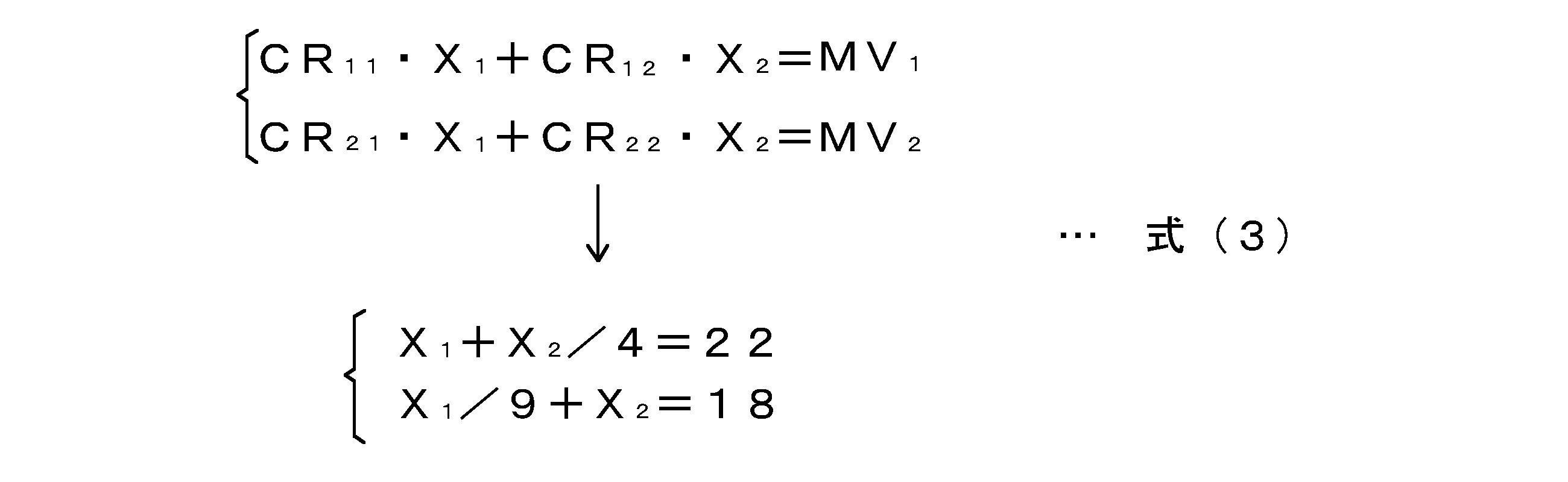
式(3)の2元連立方程式を解くと、第1有機蒸着材料31aの真の放出レート(X1)は、18Å/秒であり、第2有機蒸着材料31bの真の放出レート(X2)は、16Å/秒であることが分かる。
即ち、第1放出レートセンサ4aの測定値(MV1)と第1有機蒸着材料31aの真の放出レート(X1)は、4Å/秒の誤差があり、第2放出レートセンサ4bの測定値(MV2)と第2有機蒸着材料31bの真の放出レート(X2)は、2Å/秒の誤差がある。
このように、本発明では、蒸着源の数(n)に対応するn元連立方程式を解くことにより、各有機蒸着材料の真の放出レート(Xj)を算出することができる。
即ち、第1放出レートセンサ4aの測定値(MV1)と第1有機蒸着材料31aの真の放出レート(X1)は、4Å/秒の誤差があり、第2放出レートセンサ4bの測定値(MV2)と第2有機蒸着材料31bの真の放出レート(X2)は、2Å/秒の誤差がある。
このように、本発明では、蒸着源の数(n)に対応するn元連立方程式を解くことにより、各有機蒸着材料の真の放出レート(Xj)を算出することができる。
(第3蒸着工程)
第3蒸着工程は、第2蒸着工程で算出した各有機蒸着材料の真の放出レート(Xj)と各有機蒸着材料の目標放出レート(TRj)との偏差が小さくなるように、各有機蒸着材料の放出条件をフィードバック制御する工程である。目標放出レート(TRj)は、蒸着膜の用途等に合わせて任意に設定することができる。
本工程では、算出した各有機蒸着材料の真の放出レート(Xj)が各有機蒸着材料の目標放出レート(TRj)と異なる場合、両レートが一致するように各有機蒸着材料の放出条件が逐次変更される。
真の放出レート(Xj)と各有機蒸着材料の目標放出レート(TRj)との偏差の絶対値は、目標放出レートの5%以内であることが好ましく、より好ましくは3%以内であり、特に好ましくは2%以内である。
第3蒸着工程は、第2蒸着工程で算出した各有機蒸着材料の真の放出レート(Xj)と各有機蒸着材料の目標放出レート(TRj)との偏差が小さくなるように、各有機蒸着材料の放出条件をフィードバック制御する工程である。目標放出レート(TRj)は、蒸着膜の用途等に合わせて任意に設定することができる。
本工程では、算出した各有機蒸着材料の真の放出レート(Xj)が各有機蒸着材料の目標放出レート(TRj)と異なる場合、両レートが一致するように各有機蒸着材料の放出条件が逐次変更される。
真の放出レート(Xj)と各有機蒸着材料の目標放出レート(TRj)との偏差の絶対値は、目標放出レートの5%以内であることが好ましく、より好ましくは3%以内であり、特に好ましくは2%以内である。
放出条件の変更は、各放出レートセンサの測定値(MVi)が変動するものであれば特に限定されず、例えば、各蒸着源の加熱温度や、収容器の開口度の変更が挙げられる。例えば、第j有機蒸着材料の真の放出レート(Xj)がその目標放出レート(TRj)よりも低い場合、第j有機蒸着源の加熱温度や収容器の開口度を高くし、第j有機蒸着材料の真の放出レート(Xj)がその目標放出レート(TRj)よりも高い場合、第j蒸着源の加熱温度や収容器の開口度を低くするように放出条件を変更する。
放出条件を変更することで各放出レートセンサの測定値(MVi)が変動し、それに合わせて各有機蒸着材料の真の放出レート(Xj)も変動する。このように放出条件の変更を逐次行うことにより、各有機蒸着材料の真の放出レート(Xj)がその目標放出レート(TRj)と一致するようにフィードバック制御が行われる。このフィードバック制御により、最終的に、各有機蒸着材料を目標放出レート(TRj)にてチャンバー内に放出することができる。
放出条件を変更することで各放出レートセンサの測定値(MVi)が変動し、それに合わせて各有機蒸着材料の真の放出レート(Xj)も変動する。このように放出条件の変更を逐次行うことにより、各有機蒸着材料の真の放出レート(Xj)がその目標放出レート(TRj)と一致するようにフィードバック制御が行われる。このフィードバック制御により、最終的に、各有機蒸着材料を目標放出レート(TRj)にてチャンバー内に放出することができる。
図6は、蒸着工程のフロー図である。図6において、「全蒸着源の加熱」及び「放出レート(MVi)の検出」が、第1蒸着工程に相当し、「真の放出レート(Xj)の算出」が、第2蒸着工程に相当し、それ以降の工程が、第3蒸着工程に相当する。
第3蒸着工程以降、蒸着工程を終了するか否かの条件は特に限定されず、形成する有機蒸着膜の機能や用途に合わせて任意に設定することができる。例えば、真の放出レート(Xj)と目標放出レート(TRj)が一致してから数秒後に蒸着工程を終了するように設定することができる。また、図2に示すように、長尺状の基材をチャンバー内で送り出しつつ共蒸着を行う場合、送り出される基材が尽きた段階で蒸着工程を終了するように設定することもできる。
第3蒸着工程以降、蒸着工程を終了するか否かの条件は特に限定されず、形成する有機蒸着膜の機能や用途に合わせて任意に設定することができる。例えば、真の放出レート(Xj)と目標放出レート(TRj)が一致してから数秒後に蒸着工程を終了するように設定することができる。また、図2に示すように、長尺状の基材をチャンバー内で送り出しつつ共蒸着を行う場合、送り出される基材が尽きた段階で蒸着工程を終了するように設定することもできる。
本発明では、基材をチャンバー内に導入するタイミングは特に限定されない。基材は、前工程中(第1前工程~第3前工程中)又は蒸着工程中(第1蒸着工程から第3蒸着工程中)に導入されてもよく、前工程より前に導入されてもよい。
好ましくは、基材は、第3蒸着工程中にチャンバー内に導入される。第3蒸着工程より前では、各有機蒸着材料の放出条件がフィードバック制御されていないため、基材に付着する各有機蒸着材料の量が不均等になるためである。
第3蒸着工程中に基材をチャンバー内に導入する場合、図2のような蒸着膜製造装置1を用いるのであれば、基材5を導入する直前まで、第2ロールBの蒸着エリア21に露出した表面がカバー部材(図示せず)によって覆われていることが好ましい。基材5をチャンバー2に導入する前に第2ロールBの表面に有機蒸着材料が付着すると、基材5の適切な送り出しが阻害される虞があるためである。
また、第3蒸着工程より前に基材5をチャンバー内に導入する場合、第3蒸着工程中に基材をチャンバー内に導入する場合と同様に、基材5を導入する直前まで、第2ロールBの表面がカバー部材によって覆われていてもよいが、基材5自体をカバー部材として利用することもできる。即ち、チャンバーに導入した基材5によって第2ロールBの表面を覆うことにより第2ロールBの表面に有機蒸着材料が付着することを防止できる。
もっとも、基材5自体をカバー部材として利用する場合、第3蒸着工程で各有機蒸着材料の放出条件がフィードバック制御されるまで、基材5をチャンバー内で送り出さないことが好ましい。基材5をチャンバー内で送り出さないことにより、蒸着エリア21に露出した基材5の一部にのみ有機蒸着材料が付着し、カバー部材として用いられる基材5の面積を最小限に抑えることができる。カバー部材として用いられた基材5の一部は、目標放出レートを反映しない蒸着量の有機蒸着材料が付着している。そのため、カバー部材として用いられた基材5の一部は、通常、基材5全体に有機蒸着膜を形成した後に破棄される。
好ましくは、基材は、第3蒸着工程中にチャンバー内に導入される。第3蒸着工程より前では、各有機蒸着材料の放出条件がフィードバック制御されていないため、基材に付着する各有機蒸着材料の量が不均等になるためである。
第3蒸着工程中に基材をチャンバー内に導入する場合、図2のような蒸着膜製造装置1を用いるのであれば、基材5を導入する直前まで、第2ロールBの蒸着エリア21に露出した表面がカバー部材(図示せず)によって覆われていることが好ましい。基材5をチャンバー2に導入する前に第2ロールBの表面に有機蒸着材料が付着すると、基材5の適切な送り出しが阻害される虞があるためである。
また、第3蒸着工程より前に基材5をチャンバー内に導入する場合、第3蒸着工程中に基材をチャンバー内に導入する場合と同様に、基材5を導入する直前まで、第2ロールBの表面がカバー部材によって覆われていてもよいが、基材5自体をカバー部材として利用することもできる。即ち、チャンバーに導入した基材5によって第2ロールBの表面を覆うことにより第2ロールBの表面に有機蒸着材料が付着することを防止できる。
もっとも、基材5自体をカバー部材として利用する場合、第3蒸着工程で各有機蒸着材料の放出条件がフィードバック制御されるまで、基材5をチャンバー内で送り出さないことが好ましい。基材5をチャンバー内で送り出さないことにより、蒸着エリア21に露出した基材5の一部にのみ有機蒸着材料が付着し、カバー部材として用いられる基材5の面積を最小限に抑えることができる。カバー部材として用いられた基材5の一部は、目標放出レートを反映しない蒸着量の有機蒸着材料が付着している。そのため、カバー部材として用いられた基材5の一部は、通常、基材5全体に有機蒸着膜を形成した後に破棄される。
本発明の有機蒸着膜の製造方法を用いれば、各有機蒸着材料を所望の放出レート(目標放出レート)にてチャンバー内に放出することができるため、基材に対する各有機蒸着材料の蒸着量を正確に制御でき、その結果、各有機蒸着材料を所望の比率で含んだ有機蒸着膜を形成することができる。
また、本発明によって形成される有機蒸着膜は有機エレクトロルミネッセンス装置の発光層として用いることができる。この発光層は、各有機蒸着材料を所望の比率で含むため、発光機能に優れる。
また、本発明によって形成される有機蒸着膜は有機エレクトロルミネッセンス装置の発光層として用いることができる。この発光層は、各有機蒸着材料を所望の比率で含むため、発光機能に優れる。
本発明の第1実施形態では、図2に示すように、2個の蒸着源を有する蒸着膜製造装置を使用したが、本発明で用いられる蒸着膜製造装置は、第1実施形態で用いたものに限定されない。以下、本発明の第2実施形態で用いられる蒸着膜製造装置について説明するが、主として、第1実施形態の蒸着膜製造装置と異なる部分についてのみ言及する。
図7は、本発明の第2実施形態で用いられる蒸着膜製造装置1を表す概要図である。
本実施形態では、チャンバー2は、その内部に放出口61を有する混合室6を有する。チャンバー2内において、混合室6の内側と外側は、該放出口61を介して連通している。混合室6は、n個の蒸着源3に含まれるn種類の有機蒸着材料31を混合するために設けられた室であり、n個の蒸着源3の各収容器32は、混合室6に筒状部材7を介して連通されている。なお、図7では、各蒸着源3は、チャンバー2の外側に設けられているが、各蒸着源3は、チャンバー2の内部に設けられていてもよい(図示せず)。また、図7では、蒸着源3の数は3個(第1蒸着源3a~第3蒸着源3c)であるが、蒸着源3の数は2個であってもよく、4個以上であってもよい。
本実施形態では、チャンバー2は、その内部に放出口61を有する混合室6を有する。チャンバー2内において、混合室6の内側と外側は、該放出口61を介して連通している。混合室6は、n個の蒸着源3に含まれるn種類の有機蒸着材料31を混合するために設けられた室であり、n個の蒸着源3の各収容器32は、混合室6に筒状部材7を介して連通されている。なお、図7では、各蒸着源3は、チャンバー2の外側に設けられているが、各蒸着源3は、チャンバー2の内部に設けられていてもよい(図示せず)。また、図7では、蒸着源3の数は3個(第1蒸着源3a~第3蒸着源3c)であるが、蒸着源3の数は2個であってもよく、4個以上であってもよい。
筒状部材7は、その内側に気化した有機蒸着材料が通り抜け可能な空洞部71を有しており、さらに、この空洞部71の幅を任意に変更可能なバルブ部72を有する。バルブ部72の構造は特に限定されないが、例えば、図7に示すように、筒状部材の外周面から空洞部にまで貫通した栓部721と、栓部721の端部(空洞部71の外側に露出した部分)に設けられた棒部722と、を有する。この栓部721を筒状部材7の空洞部71に押し入れる又は空洞部71から引き抜くことにより、空洞部71の幅が任意に変更でき、各有機蒸着材料31が混合室内に流入する量を調整することができる。
本実施形態では、チャンバー2内で且つ混合室6の外側にある筒状部材7の外周面に微細孔(ピンホール)が設けられ(図示せず)、該微細孔の近傍に各放出レートセンサ4が設けられている。微細孔から漏れ出した各有機蒸着材料31に基づき、各放出レートセンサ4が各有機蒸着材料31の放出レートを測定する。
なお、各放出レートセンサ4は、混合室6の内側であって筒状部材7の端部近傍に設けられていてもよい(図示せず)。本発明では、放出レートセンサ4の位置に関わらず、各有機蒸着材料31の真の放出レートを算出することができる。
本実施形態では、チャンバー2内で且つ混合室6の外側にある筒状部材7の外周面に微細孔(ピンホール)が設けられ(図示せず)、該微細孔の近傍に各放出レートセンサ4が設けられている。微細孔から漏れ出した各有機蒸着材料31に基づき、各放出レートセンサ4が各有機蒸着材料31の放出レートを測定する。
なお、各放出レートセンサ4は、混合室6の内側であって筒状部材7の端部近傍に設けられていてもよい(図示せず)。本発明では、放出レートセンサ4の位置に関わらず、各有機蒸着材料31の真の放出レートを算出することができる。
本実施形態では、各蒸着源3から各筒状部材7を通って混合室6に流入した各有機蒸着材料31は、混合室6で混合される。その後、混合された有機蒸着材料31は、放出口61から放出され、基材5の表面に付着する。
放出口61と基材5の表面の距離Dは、特に限定されないが、好ましくは、10mm以下であり、より好ましくは5mm以下であり、特に好ましくは1mm以下である。また、距離Dの下限値は特に限定されないが、現実的には、0.5mm以上である。距離Dが短ければ短いほど、短時間で基材5の表面に蒸着膜を形成することができる。
なお、放出口61と基材5の表面が近い場合、短時間で蒸着膜が形成されるため、各有機蒸着材料31のチャンバー2内における放出量の調整は非常に重要となる。この点、本発明の蒸着膜の製造方法を用いれば、各有機蒸着材料31の真の放出レートXjが目標放出レートTRjと略一致するため、所望の比率で各有機蒸着材料31を含んだ蒸着膜を高精度で形成することができる。
放出口61と基材5の表面の距離Dは、特に限定されないが、好ましくは、10mm以下であり、より好ましくは5mm以下であり、特に好ましくは1mm以下である。また、距離Dの下限値は特に限定されないが、現実的には、0.5mm以上である。距離Dが短ければ短いほど、短時間で基材5の表面に蒸着膜を形成することができる。
なお、放出口61と基材5の表面が近い場合、短時間で蒸着膜が形成されるため、各有機蒸着材料31のチャンバー2内における放出量の調整は非常に重要となる。この点、本発明の蒸着膜の製造方法を用いれば、各有機蒸着材料31の真の放出レートXjが目標放出レートTRjと略一致するため、所望の比率で各有機蒸着材料31を含んだ蒸着膜を高精度で形成することができる。
以下、実施例を示して本発明をさらに説明する。ただし、本発明は、下記実施例のみに限定されるものではない。
(準備工程)
本発明の第2実施形態で用いた混合室を有する蒸着膜製造装置(図7参照)を準備した。蒸着源の数は3個であった。チャンバー内の真空度は、4×10⁻⁴Paに設定した。
第1蒸着源に含まれる第1有機蒸着材料として、Alq3を用いた。第2蒸着源に含まれる第2有機蒸着材料として、Ir(pq)2(acac)を用いた。第3蒸着源に含まれる第3有機蒸着材料として、N,N’-ビス(ナフタレン-1-イル)-N,N’-ビス(フェニル)-2,2’-ジメチルベンジジン(略称:α-NPD)を用いた。
なお、本実施例において、後述する開口度は、バルブ部を押し入れない場合における空洞部の幅(100%)を基準にしており、バルブを押し入れる又は引き抜くことで開口度を調整した。以下、第n蒸着源に対応するバルブ部を第nバルブ部と称する。
本発明の第2実施形態で用いた混合室を有する蒸着膜製造装置(図7参照)を準備した。蒸着源の数は3個であった。チャンバー内の真空度は、4×10⁻⁴Paに設定した。
第1蒸着源に含まれる第1有機蒸着材料として、Alq3を用いた。第2蒸着源に含まれる第2有機蒸着材料として、Ir(pq)2(acac)を用いた。第3蒸着源に含まれる第3有機蒸着材料として、N,N’-ビス(ナフタレン-1-イル)-N,N’-ビス(フェニル)-2,2’-ジメチルベンジジン(略称:α-NPD)を用いた。
なお、本実施例において、後述する開口度は、バルブ部を押し入れない場合における空洞部の幅(100%)を基準にしており、バルブを押し入れる又は引き抜くことで開口度を調整した。以下、第n蒸着源に対応するバルブ部を第nバルブ部と称する。
(前工程)
第1蒸着源のみを320℃に加熱し、第1バルブ部の開口度を0%~70%まで5.0%毎に5秒間隔で経時的に変更した後、再び70%~0%まで5.0%毎に5秒間隔で経時的に変更した。なお、第2及び第3バルブ部の開口度は常に100%とした。
図8(a)は、その間における第1放出レートセンサ~第3放出レートセンサの測定値(PMV1~PMV3)を経時的にプロットしたグラフであり、図8(b)は、その間における第2放出レートセンサに対する第1有機蒸着材料の混入率(CR21)及び第3放出レートセンサに対する第1有機蒸着材料の混入率(CR31)の値を経時的にプロットしたグラフである。CR21は、0.050で略一定であり、CR31は、0.056で略一定であった。
なお、開口度0%~15%及び15%~0の間は、第2及び第3放出レートセンサに混入する第1有機蒸着材料の量が極めて微量であるため、CR21及びCR31を算出しなかった。
第1蒸着源のみを320℃に加熱し、第1バルブ部の開口度を0%~70%まで5.0%毎に5秒間隔で経時的に変更した後、再び70%~0%まで5.0%毎に5秒間隔で経時的に変更した。なお、第2及び第3バルブ部の開口度は常に100%とした。
図8(a)は、その間における第1放出レートセンサ~第3放出レートセンサの測定値(PMV1~PMV3)を経時的にプロットしたグラフであり、図8(b)は、その間における第2放出レートセンサに対する第1有機蒸着材料の混入率(CR21)及び第3放出レートセンサに対する第1有機蒸着材料の混入率(CR31)の値を経時的にプロットしたグラフである。CR21は、0.050で略一定であり、CR31は、0.056で略一定であった。
なお、開口度0%~15%及び15%~0の間は、第2及び第3放出レートセンサに混入する第1有機蒸着材料の量が極めて微量であるため、CR21及びCR31を算出しなかった。
次に、第2蒸着源のみを300℃に加熱し、第2バルブ部の開口度を0%~70%まで5.0%毎に5秒間隔で経時的に変更した後、再び70%~0%まで5.0%毎に5秒間隔で経時的に変更した。なお、第1及び第3バルブ部の開口度は常に100%とした。
図9(a)は、その間における第1放出レートセンサ~第3放出レートセンサの測定値(PMV1~PMV3)を経時的にプロットしたグラフであり、図9(b)は、その間における第1放出レートセンサに対する第2有機蒸着材料の混入率(CR12)及び第3放出レートセンサに対する第2有機蒸着材料の混入率(CR32)の値を経時的にプロットしたグラフである。CR12は、0.280で略一定であり、CR32は、0.242で略一定であった。
なお、開口度0%~20%及び20%~0の間は、第1及び第3放出レートセンサに混入する第2有機蒸着材料の量が極めて微量であるため、CR12及びCR32を算出しなかった。
図9(a)は、その間における第1放出レートセンサ~第3放出レートセンサの測定値(PMV1~PMV3)を経時的にプロットしたグラフであり、図9(b)は、その間における第1放出レートセンサに対する第2有機蒸着材料の混入率(CR12)及び第3放出レートセンサに対する第2有機蒸着材料の混入率(CR32)の値を経時的にプロットしたグラフである。CR12は、0.280で略一定であり、CR32は、0.242で略一定であった。
なお、開口度0%~20%及び20%~0の間は、第1及び第3放出レートセンサに混入する第2有機蒸着材料の量が極めて微量であるため、CR12及びCR32を算出しなかった。
次に、第3蒸着源のみを280℃に加熱し、第3バルブ部の開口度を0%~70%まで5.0%毎に5秒間隔で経時的に変更した後、再び70%~0%まで5.0%毎に5秒間隔で経時的に変更した。なお、第1及び第2バルブ部の開口度は常に100%とした。
図10(a)は、その間における第1放出レートセンサ~第3放出レートセンサの測定値(PMV1~PMV3)を経時的にプロットしたグラフであり、図10(b)は、その間における第1放出レートセンサに対する第3有機蒸着材料の混入率(CR13)及び第2放出レートセンサに対する第3有機蒸着材料の混入率(CR23)の値を経時的にプロットしたグラフである。CR13は、0.067で略一定であり、CR23は、0.053で略一定であった。
なお、開口度0%~15%及び15%~0の間は、第1及び第2放出レートセンサに混入する第3有機蒸着材料の量が極めて微量であるため、CR13及びCR23を算出しなかった。
図10(a)は、その間における第1放出レートセンサ~第3放出レートセンサの測定値(PMV1~PMV3)を経時的にプロットしたグラフであり、図10(b)は、その間における第1放出レートセンサに対する第3有機蒸着材料の混入率(CR13)及び第2放出レートセンサに対する第3有機蒸着材料の混入率(CR23)の値を経時的にプロットしたグラフである。CR13は、0.067で略一定であり、CR23は、0.053で略一定であった。
なお、開口度0%~15%及び15%~0の間は、第1及び第2放出レートセンサに混入する第3有機蒸着材料の量が極めて微量であるため、CR13及びCR23を算出しなかった。
図8(a)、図9(a)、及び図10(a)の結果から、加熱した第j有機蒸着材料の放出レートが上がれば上がるほど、第n放出レートセンサに対する第j有機蒸着材料の混入量が増えることが分かる。
また、図8(b)、図9(b)、及び図10(b)の結果から、第j有機蒸着材料の放出レートが変動しても、第i放出レートセンサに対する第j有機蒸着材料の混入率(CRij)は、略一定であることが読み取れる。
また、図8(b)、図9(b)、及び図10(b)の結果から、第j有機蒸着材料の放出レートが変動しても、第i放出レートセンサに対する第j有機蒸着材料の混入率(CRij)は、略一定であることが読み取れる。
(蒸着工程)
次に、第1~第3蒸着源を全て加熱し、第1~第3放出レートセンサの測定値(MV1~MV3)を検出した。各放出レートセンサの測定値(MV1~MV3)と前工程で得られた混入率(CR21、CR31、CR12、CR32、CR13、及びCR23)を基に、各有機蒸着材料の真の放出レート(X1~X3)を算出し、この真の放出レート(X1~X3)が各有機蒸着材料の目標放出レート(TR1~TR3)となるように各有機蒸着材料の放出条件を逐次変更するフィードバック制御を行った。その結果を、図11(a)及び図11(b)に表す。図11(b)は、図11(a)から、第1~第3放出レートセンサの測定値(MV1~MV3)を除き、第1~第3有機蒸着材料の目標放出レート(TR1~TR3)を破線で表したグラフである。
なお、放出条件の変更には、第1~第3バルブ部の開口度の変更、及び、第1~第3蒸着源の加熱温度の変更を採用した。
図11(b)の結果から、約100秒後には、真の放出レート(X1~3)が各有機蒸着材料の目標放出レート(TR1~3)に略一致していることが読み取れる。
次に、第1~第3蒸着源を全て加熱し、第1~第3放出レートセンサの測定値(MV1~MV3)を検出した。各放出レートセンサの測定値(MV1~MV3)と前工程で得られた混入率(CR21、CR31、CR12、CR32、CR13、及びCR23)を基に、各有機蒸着材料の真の放出レート(X1~X3)を算出し、この真の放出レート(X1~X3)が各有機蒸着材料の目標放出レート(TR1~TR3)となるように各有機蒸着材料の放出条件を逐次変更するフィードバック制御を行った。その結果を、図11(a)及び図11(b)に表す。図11(b)は、図11(a)から、第1~第3放出レートセンサの測定値(MV1~MV3)を除き、第1~第3有機蒸着材料の目標放出レート(TR1~TR3)を破線で表したグラフである。
なお、放出条件の変更には、第1~第3バルブ部の開口度の変更、及び、第1~第3蒸着源の加熱温度の変更を採用した。
図11(b)の結果から、約100秒後には、真の放出レート(X1~3)が各有機蒸着材料の目標放出レート(TR1~3)に略一致していることが読み取れる。
1…蒸着膜製造装置、2…チャンバー、3…蒸着源、31…蒸着材料、32…収容器、4…放出レートセンサ、5…基材、6…混合室、61…放出口、7…筒状部材、71…空洞部、72…バルブ部
Claims (8)
- 内部を真空状態に保持したチャンバーと、前記チャンバー内に放出する有機蒸着材料を含むn個の蒸着源と、前記n個の蒸着源に対応して前記有機蒸着材料の放出レートを測定するn個の放出レートセンサと、を有する蒸着膜製造装置を準備する準備工程と、
前記蒸着膜製造装置を用いて、各放出レートセンサに対する各有機蒸着材料の混入率を算出する前工程と、
全ての有機蒸着材料を同時に前記チャンバー内に放出することにより、前記チャンバー内に導入した基材の表面に有機蒸着膜を形成する蒸着工程と、を有し、
前記前工程が、
前記n個の蒸着源から選択した1個の第j蒸着源のみを加熱し、前記第j蒸着源に含まれる第j有機蒸着材料を前記チャンバー内に放出する第1前工程と、
前記第1前工程で加熱した前記第j蒸着源に対応する第j放出レートセンサの測定値(PMVj)及び第i蒸着源に対応する第i放出レートセンサの測定値(PMVi)に基づき、下記式(1)で表される前記第i放出レートセンサに対する前記第j有機蒸着材料の混入率(CRij)を全ての放出レートセンサについて算出する第2前工程と、
前記第j蒸着源を変更し、前記第1及び第2前工程と同じ工程を繰り返すことにより、全ての放出レートセンサに対する各有機蒸着材料の混入率を全ての有機蒸着材料について算出する第3前工程と、を有し、

全ての蒸着源を加熱し、各蒸着源に対応する各放出レートセンサの測定値(MVi)を検出する第1蒸着工程と、
前記第3前工程で算出した全ての放出レートセンサに対する全ての有機蒸着材料の混入率、及び、前記第1蒸着工程で検出した各放出レートセンサの測定値(MVi)を用いて、下記式(2)に基づき、各有機蒸着材料の真の放出レート(Xj)を算出する第2蒸着工程と、
前記第2蒸着工程で算出した各有機蒸着材料の真の放出レート(Xj)と各有機蒸着材料の目標放出レート(TRj)との偏差が小さくなるように、各有機蒸着材料の放出条件をフィードバック制御する第3蒸着工程と、を有することを特徴とする有機蒸着膜の製造方法。

- 前記n個の蒸着源のそれぞれが、有機蒸着材料を収容した収容器を有しており、
前記チャンバーが、その内側に、放出口を有する混合室を有しており、
前記n個の蒸着源の各収容器が、前記混合室に連通されており、
前記蒸着工程において、前記n個の蒸着源に含まれる各有機蒸着材料を前記混合室で混合し、且つ、前記混合した有機蒸着材料を前記放出口から基材の表面に向かって放出する、請求項1に記載の有機蒸着膜の製造方法。 - 前記n個の蒸着源の各収容器が、気化した有機蒸着材料が通り抜け可能な空洞部を有する筒状部材を介して前記混合室に連通されており、
前記筒状部材が、前記空洞部の幅を任意に変更可能なバルブ部を有する、請求項2に記載の有機蒸着膜の製造方法。 - 前記第3蒸着工程において、各蒸着源の加熱温度を変更することにより、各有機蒸着材料の放出条件をフィードバック制御する、請求項1乃至3の何れか一項に記載の有機蒸着膜の製造方法。
- 前記第3蒸着工程において、前記バルブ部を用いて前記空洞部の幅を変更することにより、各有機蒸着材料の放出条件をフィードバック制御する、請求項3又は4に記載の有機蒸着膜の製造方法。
- 前記蒸着工程において、前記混合室の放出口と前記基材の距離が10mm以下である、請求項2乃至5の何れか一項に記載の有機蒸着膜の製造方法。
- 前記チャンバー内の真空度が10-3Pa以下である、請求項1乃至6の何れか一項に記載の有機蒸着膜の製造方法。
- 請求項1乃至7の何れか一項に記載の有機蒸着膜の製造方法によって形成された有機蒸着膜を発光層として有する有機エレクトロルミネッセンス装置。
Applications Claiming Priority (2)
| Application Number | Priority Date | Filing Date | Title |
|---|---|---|---|
| JP2015005394A JP2018070896A (ja) | 2015-01-14 | 2015-01-14 | 有機蒸着膜の製造方法及び有機エレクトロルミネッセンス装置 |
| JP2015-005394 | 2015-01-14 |
Publications (1)
| Publication Number | Publication Date |
|---|---|
| WO2016114225A1 true WO2016114225A1 (ja) | 2016-07-21 |
Family
ID=56405772
Family Applications (1)
| Application Number | Title | Priority Date | Filing Date |
|---|---|---|---|
| PCT/JP2016/050441 Ceased WO2016114225A1 (ja) | 2015-01-14 | 2016-01-08 | 有機蒸着膜の製造方法及び有機エレクトロルミネッセンス装置 |
Country Status (2)
| Country | Link |
|---|---|
| JP (1) | JP2018070896A (ja) |
| WO (1) | WO2016114225A1 (ja) |
Citations (4)
| Publication number | Priority date | Publication date | Assignee | Title |
|---|---|---|---|---|
| JP2004079528A (ja) * | 2002-08-01 | 2004-03-11 | Semiconductor Energy Lab Co Ltd | 製造装置 |
| JP2012107287A (ja) * | 2010-11-17 | 2012-06-07 | Ulvac Japan Ltd | 薄膜形成装置 |
| WO2013111599A1 (ja) * | 2012-01-26 | 2013-08-01 | パナソニック株式会社 | 真空蒸着装置 |
| JP2015001013A (ja) * | 2013-06-17 | 2015-01-05 | 日東電工株式会社 | 成膜装置及び有機elデバイスの製造方法 |
-
2015
- 2015-01-14 JP JP2015005394A patent/JP2018070896A/ja active Pending
-
2016
- 2016-01-08 WO PCT/JP2016/050441 patent/WO2016114225A1/ja not_active Ceased
Patent Citations (4)
| Publication number | Priority date | Publication date | Assignee | Title |
|---|---|---|---|---|
| JP2004079528A (ja) * | 2002-08-01 | 2004-03-11 | Semiconductor Energy Lab Co Ltd | 製造装置 |
| JP2012107287A (ja) * | 2010-11-17 | 2012-06-07 | Ulvac Japan Ltd | 薄膜形成装置 |
| WO2013111599A1 (ja) * | 2012-01-26 | 2013-08-01 | パナソニック株式会社 | 真空蒸着装置 |
| JP2015001013A (ja) * | 2013-06-17 | 2015-01-05 | 日東電工株式会社 | 成膜装置及び有機elデバイスの製造方法 |
Also Published As
| Publication number | Publication date |
|---|---|
| JP2018070896A (ja) | 2018-05-10 |
Similar Documents
| Publication | Publication Date | Title |
|---|---|---|
| Shtein et al. | Material transport regimes and mechanisms for growth of molecular organic thin films using low-pressure organic vapor phase deposition | |
| TWI409346B (zh) | 蒸鍍源、蒸鍍裝置、成膜方法 | |
| TWI433947B (zh) | 真空氣相沉積系統 | |
| KR101496667B1 (ko) | 진공 증착장치 | |
| US6558736B2 (en) | Low pressure vapor phase deposition of organic thin films | |
| TWI428459B (zh) | 蒸鍍源,蒸鍍裝置,有機薄膜的成膜方法 | |
| US20130209666A1 (en) | Evaporating apparatus and evaporating method | |
| JP5506147B2 (ja) | 成膜装置及び成膜方法 | |
| JP2009087931A (ja) | 成膜方法、蒸着装置、有機el製造装置 | |
| WO2008038821A1 (fr) | appareil de déposition, appareil de commande d'appareil de déposition, procédé de commande d'appareil de déposition, appareil de déposition utilisant ce procédé et procédé de fabrication de sortie | |
| CN106103790B (zh) | 蒸镀装置及其控制方法、使用了蒸镀装置的蒸镀方法、以及器件的制造方法 | |
| JP3756458B2 (ja) | 薄膜堆積用分子線源セル | |
| US8899174B2 (en) | Device and method for fabricating display device | |
| WO2015118936A1 (ja) | 発光層の製造方法、発光層および有機発光素子 | |
| US20050281948A1 (en) | Vaporizing temperature sensitive materials | |
| WO2016114225A1 (ja) | 有機蒸着膜の製造方法及び有機エレクトロルミネッセンス装置 | |
| KR101191690B1 (ko) | 증착원, 증착 장치, 유기 박막의 성막 방법 | |
| CN100385035C (zh) | 形成有机薄膜的方法 | |
| KR102062864B1 (ko) | 페로브스카이트 발광소자 증착 시스템, 발광소자와 그 제조 방법 | |
| JP5460773B2 (ja) | 成膜装置及び成膜方法 | |
| JP2005029885A (ja) | 薄膜形成方法および薄膜形成装置並びに半導体デバイス | |
| JP2017082272A (ja) | 蒸着膜の製造方法及び蒸着装置 | |
| KR20120138305A (ko) | 유기 박막 증착 시스템 및 유기 박막 증착 방법 | |
| Keiper et al. | Novel solutions for thin film layer deposition for organic materials |
Legal Events
| Date | Code | Title | Description |
|---|---|---|---|
| 121 | Ep: the epo has been informed by wipo that ep was designated in this application |
Ref document number: 16737296 Country of ref document: EP Kind code of ref document: A1 |
|
| NENP | Non-entry into the national phase |
Ref country code: DE |
|
| 122 | Ep: pct application non-entry in european phase |
Ref document number: 16737296 Country of ref document: EP Kind code of ref document: A1 |
|
| NENP | Non-entry into the national phase |
Ref country code: JP |