WO2016106902A1 - 液晶面板的驱动方法 - Google Patents
液晶面板的驱动方法 Download PDFInfo
- Publication number
- WO2016106902A1 WO2016106902A1 PCT/CN2015/071216 CN2015071216W WO2016106902A1 WO 2016106902 A1 WO2016106902 A1 WO 2016106902A1 CN 2015071216 W CN2015071216 W CN 2015071216W WO 2016106902 A1 WO2016106902 A1 WO 2016106902A1
- Authority
- WO
- WIPO (PCT)
- Prior art keywords
- liquid crystal
- crystal panel
- driving voltage
- driving
- stage
- Prior art date
Links
Images
Classifications
-
- G—PHYSICS
- G06—COMPUTING; CALCULATING OR COUNTING
- G06F—ELECTRIC DIGITAL DATA PROCESSING
- G06F3/00—Input arrangements for transferring data to be processed into a form capable of being handled by the computer; Output arrangements for transferring data from processing unit to output unit, e.g. interface arrangements
- G06F3/01—Input arrangements or combined input and output arrangements for interaction between user and computer
- G06F3/03—Arrangements for converting the position or the displacement of a member into a coded form
- G06F3/041—Digitisers, e.g. for touch screens or touch pads, characterised by the transducing means
- G06F3/0412—Digitisers structurally integrated in a display
-
- G—PHYSICS
- G09—EDUCATION; CRYPTOGRAPHY; DISPLAY; ADVERTISING; SEALS
- G09G—ARRANGEMENTS OR CIRCUITS FOR CONTROL OF INDICATING DEVICES USING STATIC MEANS TO PRESENT VARIABLE INFORMATION
- G09G3/00—Control arrangements or circuits, of interest only in connection with visual indicators other than cathode-ray tubes
- G09G3/20—Control arrangements or circuits, of interest only in connection with visual indicators other than cathode-ray tubes for presentation of an assembly of a number of characters, e.g. a page, by composing the assembly by combination of individual elements arranged in a matrix no fixed position being assigned to or needed to be assigned to the individual characters or partial characters
- G09G3/2007—Display of intermediate tones
- G09G3/2077—Display of intermediate tones by a combination of two or more gradation control methods
-
- G—PHYSICS
- G09—EDUCATION; CRYPTOGRAPHY; DISPLAY; ADVERTISING; SEALS
- G09G—ARRANGEMENTS OR CIRCUITS FOR CONTROL OF INDICATING DEVICES USING STATIC MEANS TO PRESENT VARIABLE INFORMATION
- G09G3/00—Control arrangements or circuits, of interest only in connection with visual indicators other than cathode-ray tubes
- G09G3/20—Control arrangements or circuits, of interest only in connection with visual indicators other than cathode-ray tubes for presentation of an assembly of a number of characters, e.g. a page, by composing the assembly by combination of individual elements arranged in a matrix no fixed position being assigned to or needed to be assigned to the individual characters or partial characters
- G09G3/34—Control arrangements or circuits, of interest only in connection with visual indicators other than cathode-ray tubes for presentation of an assembly of a number of characters, e.g. a page, by composing the assembly by combination of individual elements arranged in a matrix no fixed position being assigned to or needed to be assigned to the individual characters or partial characters by control of light from an independent source
- G09G3/36—Control arrangements or circuits, of interest only in connection with visual indicators other than cathode-ray tubes for presentation of an assembly of a number of characters, e.g. a page, by composing the assembly by combination of individual elements arranged in a matrix no fixed position being assigned to or needed to be assigned to the individual characters or partial characters by control of light from an independent source using liquid crystals
- G09G3/3611—Control of matrices with row and column drivers
- G09G3/3685—Details of drivers for data electrodes
-
- G—PHYSICS
- G09—EDUCATION; CRYPTOGRAPHY; DISPLAY; ADVERTISING; SEALS
- G09G—ARRANGEMENTS OR CIRCUITS FOR CONTROL OF INDICATING DEVICES USING STATIC MEANS TO PRESENT VARIABLE INFORMATION
- G09G2310/00—Command of the display device
- G09G2310/02—Addressing, scanning or driving the display screen or processing steps related thereto
- G09G2310/0243—Details of the generation of driving signals
- G09G2310/0251—Precharge or discharge of pixel before applying new pixel voltage
-
- G—PHYSICS
- G09—EDUCATION; CRYPTOGRAPHY; DISPLAY; ADVERTISING; SEALS
- G09G—ARRANGEMENTS OR CIRCUITS FOR CONTROL OF INDICATING DEVICES USING STATIC MEANS TO PRESENT VARIABLE INFORMATION
- G09G2310/00—Command of the display device
- G09G2310/02—Addressing, scanning or driving the display screen or processing steps related thereto
- G09G2310/0264—Details of driving circuits
- G09G2310/027—Details of drivers for data electrodes, the drivers handling digital grey scale data, e.g. use of D/A converters
-
- G—PHYSICS
- G09—EDUCATION; CRYPTOGRAPHY; DISPLAY; ADVERTISING; SEALS
- G09G—ARRANGEMENTS OR CIRCUITS FOR CONTROL OF INDICATING DEVICES USING STATIC MEANS TO PRESENT VARIABLE INFORMATION
- G09G2310/00—Command of the display device
- G09G2310/06—Details of flat display driving waveforms
-
- G—PHYSICS
- G09—EDUCATION; CRYPTOGRAPHY; DISPLAY; ADVERTISING; SEALS
- G09G—ARRANGEMENTS OR CIRCUITS FOR CONTROL OF INDICATING DEVICES USING STATIC MEANS TO PRESENT VARIABLE INFORMATION
- G09G2310/00—Command of the display device
- G09G2310/08—Details of timing specific for flat panels, other than clock recovery
-
- G—PHYSICS
- G09—EDUCATION; CRYPTOGRAPHY; DISPLAY; ADVERTISING; SEALS
- G09G—ARRANGEMENTS OR CIRCUITS FOR CONTROL OF INDICATING DEVICES USING STATIC MEANS TO PRESENT VARIABLE INFORMATION
- G09G2320/00—Control of display operating conditions
- G09G2320/02—Improving the quality of display appearance
- G09G2320/0252—Improving the response speed
Definitions
- the present invention relates to a driving method of a liquid crystal panel.
- liquid crystal displays Compared with traditional displays, liquid crystal displays have the advantages of lightness, thinness, low power consumption, low radiation, etc., and are widely used in various fields such as computers, mobile phones, and automobile displays. With the wide application of liquid crystal displays, people have higher and higher requirements for the performance of liquid crystal displays.
- the dark line in the liquid crystal display panel expands with the sliding of the finger, so that the liquid crystal molecules in the liquid crystal layer are switched to In the vertical deflection or chaos state, if the liquid crystal molecules are not restored to the horizontal deflection state in time, the liquid crystal display panel will produce a dot mura, which affects the display quality of the liquid crystal display panel.
- the technical problem to be solved by the present invention is to provide a driving method of a liquid crystal panel, which can reduce the phenomenon of poor finger pressure and improve the performance of the liquid crystal display panel.
- a driving method of a liquid crystal panel wherein the liquid crystal panel includes a plurality of rows of gate lines and a plurality of rows of data lines, the gate lines and the data lines vertically intersect each other to form a plurality of pixels arranged in an array, the liquid crystal panel
- the driving method includes: when the grayscale value of the liquid crystal panel is smaller than the first grayscale, driving the data line by using a first driving voltage, wherein the first driving voltage is a normal driving corresponding to the corresponding grayscale value a voltage; when the grayscale value of the liquid crystal panel is greater than the first grayscale and less than or equal to a maximum grayscale, the driving of the data line includes a first phase and a second phase, and the first phase is in the Before the second stage, the first stage is: driving the liquid crystal panel with a second driving voltage, the second driving voltage is less than or equal to the first driving voltage, and the second stage is: driving the In the liquid crystal panel, the third driving voltage is a voltage of a normal driving corresponding to a corresponding gray scale value
- an intermediate phase is further included between the first phase and the second phase, where the intermediate phase is: A fourth driving voltage is applied, the fourth driving voltage being greater than the third driving voltage and less than a saturation voltage for boosting a response speed of the liquid crystal panel.
- first phase, the intermediate phase and the second phase occur sequentially in succession.
- first phase and the second phase occur continuously.
- the switch of the gate line of the mth row is turned on for a first period of time, and in the first period of time, the normal driving voltage of the grayscale value corresponding to the gate line of the mth row is charged. And then turning off the gate switch of the mth row, turning on the switch of the gate line of the m+nth row for a second period of time, in the second period of time, by the second driver The voltage is charged to the gate line of the m+nth row, and both m and n are natural numbers greater than or equal to 1.
- the first time period and the second time period are continuous. After the second time period ends, the gate lines of the m+1th row are charged, and the gates of the m+1th row are used.
- the invention adopts two stages of driving voltage charging, including the first stage and the second, when the gray scale value of the liquid crystal panel is greater than the first gray level and less than the maximum gray level, that is, in the high gray level stage.
- the first phase is: driving the liquid crystal panel with a second driving voltage, the second driving voltage is less than or equal to the first driving voltage, and the second phase is Driving the liquid crystal panel with a third driving voltage, and the third driving voltage is corresponding to the corresponding gray The value of the normal drive voltage.
- the normal voltage of the second stage can be close to the saturation voltage, which is beneficial to increase the transmittance of the liquid crystal panel.
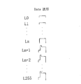
- FIG. 2 is a schematic diagram of a driving method of a liquid crystal panel according to an embodiment of the present invention.
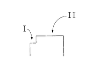
- Figure 3 is an enlarged schematic view of a Date waveform of Figure 2.
- FIG. 4 is a schematic diagram of a driving method of a liquid crystal panel according to an embodiment of the present invention.
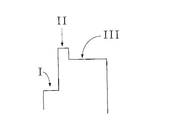
- Figure 5 is an enlarged schematic view of a Date waveform of Figure 4.
- FIG. 6 is a schematic diagram of a driving method of a liquid crystal panel according to another embodiment of the present invention.
- the present invention relates to a method for driving a liquid crystal panel.
- the liquid crystal panel includes a plurality of rows of gate lines and a plurality of rows of data lines.
- the gate lines and the data lines are perpendicularly intersected with each other to form a plurality of pixels distributed in an array.
- the row gate lines are arranged in parallel with each other along the first direction, and the plurality of rows of data lines are arranged in parallel with each other along the second direction, the first direction is perpendicular to the second direction, and the extending direction of the gate lines is regarded as the row direction, and the data lines are extended.
- the direction is treated as the column direction.
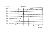
- Figure 1 shows the VT Curve of the actual product measurement of a liquid crystal panel.
- the saturation voltage is 4.5V.
- the driving voltage is changed, and the panel is pressed with a finger. It is found that when the driving voltage is lowered to 3.5V.
- the Trace mura phenomenon disappears within 2 seconds. In order to meet the specifications that Trace mura disappears within 2 seconds, it is necessary to reduce the maximum driving voltage from 4.5V to 3.5V, which is so serious.
- the transmittance of the liquid crystal display panel is lowered, and the brightness of the panel is lowered.
- the driving method of the liquid crystal panel of the present invention includes: when the gray scale value of the liquid crystal panel is smaller than the first gray scale, driving the data line by using a first driving voltage, wherein the first driving voltage is a corresponding corresponding gray The value of the normal drive voltage.
- the specific definition of the first driving voltage in the first gray-scale state is based on: when the finger presses the liquid crystal panel, the Trace mura phenomenon of the liquid crystal panel disappears within a prescribed time, and the liquid crystal panel is deemed to meet the requirements.
- the time is the time set by the user for the LCD panel, for example, 2 seconds. Different users have different rules for the disappearance of the Trace mura phenomenon after the finger pressure of the LCD panel.
- the first driving voltage is used, the Trace mura phenomenon can be specified.
- the grayscale value in this case is the first grayscale.
- the driving of the data line includes a first phase and a second phase, and the first phase is before the second phase
- the first stage is: driving the liquid crystal panel by using a second driving voltage
- the second driving voltage is less than or equal to the first driving voltage
- the second stage is: driving the liquid crystal panel by using a third driving voltage
- the third driving voltage is a normally driven voltage corresponding to a corresponding grayscale value.
- FIG. 2 includes a Date waveform
- FIG. 3 is an enlarged schematic view of a Date waveform in FIG.
- the gray scale value of the liquid crystal panel shown in FIG. 2 is from L0 to L255.
- the L0 to Lm gray scale is driven by the corresponding normal driving voltage, and the Trace mura phenomenon does not occur after the liquid crystal panel is pressed in the L0 to Lm gray scale.
- L255 is driven by the saturation voltage, and the Trace mura phenomenon occurs after the finger presses the liquid crystal panel in the gray scale of Lm to L255. Therefore, the driving method of the present invention divides the data waveform of Lm to L255 into the first stage and the second stage, that is, the driving of the data line.
- the second driving voltage employed in the first stage is 0.5 to 1.3 V smaller than the third driving voltage of the second stage, and the third driving voltage may be a saturation voltage.
- the first stage is to drive the liquid crystal panel with a voltage lower than the normal driving voltage of the corresponding gray scale value.
- the liquid crystal molecules are in a standing state, and the lower voltage is favorable for the liquid crystal molecules to recover. This eliminates trace mura, which is a phenomenon of poor finger pressure.
- the second stage uses a third driving voltage, which can be close to or equal to the saturation voltage, and can improve the transmittance of the liquid crystal display panel.
- an intermediate phase is further included between the first phase and the second phase.
- the inter-stage is: applying a fourth driving voltage, the fourth driving voltage being greater than the third driving voltage and less than a saturation voltage for increasing the response speed of the liquid crystal panel. That is to say, after a lower voltage is applied to return the liquid crystal molecules to the flat surface, a voltage value of a normal driving voltage higher than the corresponding gray scale value is applied to drive the liquid crystal panel, in order to improve the response of the liquid crystal panel. time.
- FIG. 4 includes a Date waveform
- FIG. 5 is an enlarged schematic view of a Date waveform in FIG.
- the L0 to Lm gray scale is driven by the corresponding normal driving voltage, and the Trace mura phenomenon does not occur after the liquid crystal panel is pressed in the L0 to Lm gray scale.
- the Trace mura phenomenon occurs after the finger presses the LCD panel in the Lm to L255 gray scale, and the data waveform of Lm to L255 is divided into three stages.
- the first stage (shown as I in Fig. 5) is to eliminate the low voltage of the trace mura.
- the phase shown as II in FIG.
- phase 5 is an over driver phase, that is, a fourth driving voltage is applied, and the fourth driving voltage is greater than the third driving voltage and less than a saturation voltage for boosting the response speed of the liquid crystal panel.
- the purpose of the phase is to increase the response speed of the LC, and the second phase (denoted as III in Figure 5) is the normal charging phase.
- the first phase, the intermediate phase, and the second phase occur sequentially in succession. In other words, there is no time interval between the three phases.
- the driving method does not include an intermediate stage, only the first stage and the second stage, the first stage and the second stage occurring continuously.
- the switch of the gate line of the mth row is turned on for a first time period, and the gray level corresponding to the gate line of the mth row is in the first time period.
- Charging the normal driving voltage of the value then turning off the gate switch of the mth row, turning on the switch of the gate line of the m+nth row for a second period of time, during the second period of time,
- the gate line of the m+nth row is charged with the second driving voltage, and both m and n are natural numbers greater than or equal to 1.
- the first time period and the second time period are continuous. After the second time period ends, the gate line of the m+1th row is charged, and the gate line of the m+1th row is used.
- the normal driving voltage of the corresponding grayscale value The charging time of the gate line of the m+1th row is the same as the time of the first time period. After charging the gate line of the m+1th row, the gate line of the m+1+nth row is The second driving voltage is charged, and the time for charging the gate line of the m+1+nth row is the same as the time of the second time period. Next, the above driving method is cyclically performed. The second driving voltage is lower than the normal driving voltage of the corresponding gray line value of the gate line. With such a lower voltage, the liquid crystal molecules are quickly restored to the flat state, and the trace mura is eliminated. Poor finger pressure.
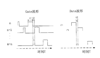
- FIG. 6 shows gate lines (Gate waveforms) and data lines (Data waveforms) from the mth to m+nth rows, and the horizontal axis represents the time T.
- Each row gate open time t1 does not immediately supply the next row of charge after the charge is turned off, but leaves a period of time t2 to perform a low potential charge on a subsequent row to eliminate the occurrence of trace mura.
- the purpose of pre-charging is to supply the m+n line with a lower potential for the liquid crystal standing after the finger is pressed to return to the flat state.
- the lower voltage and the normal voltage according to the present invention are voltages corresponding to corresponding gray scale values, and the higher the gray scale value, the larger the normal driving voltage required. Therefore, when the grayscale value is small, two stages of charging are not required, and only the corresponding normal voltage is driven, and the trace mura phenomenon does not occur. When the grayscale value is large, if it is driven by its normal voltage, the trace mura phenomenon will occur. Therefore, two stages of driving are required. First, the lower voltage is used to eliminate the trace mura phenomenon and then apply the normal voltage. .
- the invention adopts two stages of driving voltage charging, including the first stage and the second, when the gray scale value of the liquid crystal panel is greater than the first gray level and less than the maximum gray level, that is, in the high gray level stage.
- Phase before the second phase, the first phase is: driving the liquid crystal panel with a second driving voltage, the second driving voltage is less than or equal to the first driving voltage, and the second phase is Driving the liquid crystal panel with a third driving voltage, which is a normal driving voltage corresponding to a corresponding gray scale value.
- the third driving voltage of the second stage is higher, and the saturation voltage can be approached, which can improve the transmittance of the liquid crystal display panel.
Landscapes
- Engineering & Computer Science (AREA)
- Theoretical Computer Science (AREA)
- Physics & Mathematics (AREA)
- General Physics & Mathematics (AREA)
- Computer Hardware Design (AREA)
- General Engineering & Computer Science (AREA)
- Chemical & Material Sciences (AREA)
- Crystallography & Structural Chemistry (AREA)
- Human Computer Interaction (AREA)
- Control Of Indicators Other Than Cathode Ray Tubes (AREA)
- Liquid Crystal (AREA)
Abstract
一种液晶面板的驱动方法,包括:当所述液晶面板的灰阶值小于第一灰阶时,采用第一驱动电压驱动数据线,所述第一驱动电压为所对应的相应的灰阶值的正常驱动的电压;当所述液晶面板的灰阶值大于所述第一灰阶并小于或等于最大灰阶时,所述数据线的驱动包括第一阶段(I)和第二阶段(II),第一阶段(I)在所述第二阶段(II)之前,所述第一阶段(I)为:采用第二驱动电压驱动所述液晶面板,所述第二驱动电压小于等于所述第一驱动电压,第二阶段(II)为:采用第三驱动电压驱动所述液晶面板,所述第三驱动电压为对应相应的灰阶值的正常驱动的电压。该方法能够改善指压不良的现象并提升液晶显示面板的性能。
Description
本发明要求2014年12月31日递交的发明名称为“液晶面板的驱动方法”的申请号201410854121.2的在先申请优先权,上述在先申请的内容以引入的方式并入本文本中。
本发明涉及液晶面板的驱动方法。
液晶显示器相比传统的显示器,具有轻、薄、低功耗、低辐射等优点,被广泛应用于计算机、移动电话、汽车显示屏等多种领域。随着液晶显示器的广泛应用,人们对液晶显示器性能的要求越来越高。
随着液晶显示技术的发展,出现了多种显示模式的显示屏,其中IPS(In-Plane Switching,平面转换)液晶显示面板以及FFS(边缘场开关技术,Fringe Field Switching)液晶显示面板以其较高的观看视角受到广大用户的喜爱。
但是当用户用手指在IPS液晶显示面板或FFS液晶显示面板上进行滑动按压操作时,液晶显示面板中的暗线(disclition line)会随着手指的滑动扩大,这样液晶层中的液晶分子会转换到垂直偏转或混乱状态,如果不能及时让液晶分子恢复到水平偏转状态,液晶显示面板就会产生点状色斑(Trace mura),从而影响液晶显示面板的显示品质。
故,有必要提供一种液晶显示面板及液晶显示装置,以解决现有技术所存在的问题。
发明内容
本发明所要解决的技术问题在于提供一种液晶面板的驱动方法,能降改善指压不良的现象并提升液晶显示面板的性能。
为了实现上述目的,本发明实施方式提供如下技术方案:
一种液晶面板的驱动方法,所述液晶面板包括多行栅极线和多行数据线,所述栅极线与所述数据线相互垂直交叉形成多个呈阵列分布的像素,所述液晶面板的驱动方法包括:当所述液晶面板的灰阶值小于第一灰阶时,采用第一驱动电压驱动所述数据线,所述第一驱动电压为所对应的相应的灰阶值的正常驱动的电压;当所述液晶面板的灰阶值大于所述第一灰阶并小于或等于最大灰阶时,所述数据线的驱动包括第一阶段和第二阶段,第一阶段在所述第二阶段之前,所述第一阶段为:采用第二驱动电压驱动所述液晶面板,所述第二驱动电压小于等于所述第一驱动电压,第二阶段为:采用第三驱动电压驱动所述液晶面板,所述第三驱动电压为对应相应的灰阶值的正常驱动的电压。
其中,当所述液晶面板的灰阶值大于所述第一灰阶并小于最大灰阶时,在所述第一阶段和所述第二阶段之间还包括中间阶段,所述中间阶段为:施加第四驱动电压,所述第四驱动电压大于所述第三驱动电压且小于饱和电压,用以提升所述液晶面板的响应速度。
其中,所述第一阶段、所述中间阶段和所述第二阶段是依次连续发生的。
其中,所述第一阶段和所述第二阶段是连续发生的。
其中,将第m行的所述栅极线的开关打开第一时间段,在所述第一时间段内,以所述第m行的栅级线所对应的灰阶值的正常驱动电压充电,然后关闭所述第m行的所述栅极开关,将第m+n行的所述栅极线的开关打开第二时间段,在所述第二时间段内,以所述第二驱动电压为所述第m+n行的栅极线充电,m和n均为大于等于1的自然数。
其中,所述第一时间段与所述第二时间段是连续的,第二时间段结束后,对第m+1行的栅极线充电,且使用与所述第m+1行的栅极线所对应的灰阶值的正常驱动电压。
本发明通过在所述液晶面板的灰阶值大于所述第一灰阶并小于最大灰阶时,也就是在高灰阶阶段,采用两个阶段的驱动电压充电,包括第一阶段和第二阶段,第一阶段在所述第二阶段之前,所述第一阶段为:采用第二驱动电压驱动所述液晶面板,所述第二驱动电压小于等于所述第一驱动电压,第二阶段为:采用第三驱动电压驱动所述液晶面板,所述第三驱动电压为对应相应的灰
阶值的正常驱动的电压。利用第一阶段的较低的电压驱动,形成较强的水平电场,和较弱的垂直电场,有利于手指按压后站立的液晶分子回复平躺状态,从而达到改善指压不良的现象并提升液晶显示面板的性能的目的。第二阶段的正常电压可以接近饱和电压,有利于提高液晶面板的穿透率。
为了更清楚地说明本发明的技术方案,下面将对实施方式中所需要使用的附图作简单地介绍,显而易见地,下面描述中的附图仅仅是本发明的一些实施方式,对于本领域普通技术人员来讲,在不付出创造性劳动的前提下,还可以如这些附图获得其他的附图。
图1是一种液晶面板的实际产品量测的V-T Curve曲线图。
图2是本发明一种实施方式提供的液晶面板的驱动方法的示意图。
图3是图2中的一个Date波形的放大示意图。
图4是本发明一种实施方式提供的液晶面板的驱动方法的示意图。
图5是图4的一个Date波形的放大示意图。
图6是本发明另一种实施方式提供的液晶面板的驱动方法的示意图。
下面将结合本发明实施方式中的附图,对本发明实施方式中的技术方案进行清楚、完整地描述。
本发明涉及一种液晶面板的驱动方法,所述液晶面板包括多行栅极线和多行数据线,所述栅极线与所述数据线相互垂直交叉形成多个呈阵列分布的像素,多行栅极线沿着第一方向相互平行排列,多行数据线沿着第二方向相互平行排列,第一方向垂直于第二方向,栅极线的延伸方向视为行方向,数据线的延伸方向视为列方向。
图1所示为一种液晶面板的实际产品量测的V-T Curve,其饱和电压为4.5V,在液晶面板点亮后更改驱动电压,并用手指滑动按压面板,发现当驱动电压降低至3.5V时Trace mura现象2秒钟内消失。为了满足Trace mura在2秒钟内消失的规格,需要降低最高驱动电压从4.5V降低至3.5V,这样严重的
降低了液晶显示面板的穿透率,降低了面板亮度。
本发明之液晶面板的驱动方法包括:当所述液晶面板的灰阶值小于第一灰阶时,采用第一驱动电压驱动所述数据线,所述第一驱动电压为所对应的相应的灰阶值的正常驱动的电压。第一灰阶状态下的第一驱动电压的具体定义的依据为:当手指按压液晶面板时,液晶面板的Trace mura现象会在规定的时间内消失,视为液晶面板符合要求,所述规定的时间是用户针对液晶面板设定的时间,例如2秒钟,不同的用户对液晶面板的指压后Trace mura现象消失的时间规定不同,当采用第一驱动电压驱动时,Trace mura现象能够在规定的时间内消失,这种情况下的灰阶值为第一灰阶。当所述液晶面板的灰阶值大于所述第一灰阶并小于或等于最大灰阶时,所述数据线的驱动包括第一阶段和第二阶段,第一阶段在所述第二阶段之前,所述第一阶段为:采用第二驱动电压驱动所述液晶面板,所述第二驱动电压小于等于所述第一驱动电压,第二阶段为:采用第三驱动电压驱动所述液晶面板,所述第三驱动电压为对应相应的灰阶值的正常驱动的电压。
如图2和图3所示,图2中包括Date波形,图3是图2中的一个Date波形的放大示意图。图2所示的液晶面板的灰阶值从L0至L255,图中L0至Lm灰阶用所对应的正常的驱动电压驱动,在L0至Lm灰阶内按压液晶面板后不出现Trace mura现象。L255用饱和电压驱动,在Lm至L255灰阶内手指按压液晶面板后出现Trace mura现象,因此本发明的驱动方法将Lm至L255的data波形分为第Ⅰ、Ⅱ两阶段,即数据线的驱动包括第一阶段(图3中表示为I)和第二阶段(图3中表示为II)。第一阶段中的采用的第二驱动电压较第二阶段的第三驱动电压小0.5至1.3V,所述第三驱动电压可以为饱和电压。
所述第一阶段是采用较对应的灰阶值的正常驱动电压低的电压来驱动液晶面板,当手指按压液晶面板时,液晶分子呈站立状态,较低的电压有利于液晶分子恢复平躺状态,这样就消除了trace mura,即指压不良,的现象。第二阶段采用第三驱动电压,可以接近或等于饱和电压,能够提高液晶显示面板的穿透率。
本发明一种实施方式中,当所述液晶面板的灰阶值大于所述第一灰阶并小于最大灰阶时,在所述第一阶段和所述第二阶段之间还包括中间阶段,所述中
间阶段为:施加第四驱动电压,所述第四驱动电压大于所述第三驱动电压且小于饱和电压,用以提升所述液晶面板的响应速度。也就是说,在施加了一个较低的电压使得液晶分子恢复平躺后,再施加一个高于对应的灰阶值的正常驱动电压的电压值来驱动液晶面板,目的是为了提高液晶面板的响应时间。
如图4和图5所示,图4中包括Date波形,图5是图4中的一个Date波形的放大示意图。图中L0至Lm灰阶用所对应的正常的驱动电压驱动,在L0至Lm灰阶内按压液晶面板后不出现Trace mura现象。在Lm至L255灰阶内手指按压液晶面板后出现Trace mura现象,将Lm至L255的data波形分为三个阶段,第一阶段(图5中表示为I)为消除trace mura的低电压,中间阶段(图5中表示为II)为over driver阶段,即施加第四驱动电压,所述第四驱动电压大于所述第三驱动电压且小于饱和电压,用以提升所述液晶面板的响应速度此阶段目的是提高LC的响应速度,第二阶段(图5中表示为III)为正常充电阶段。
具体而言,一种实施方式中,所述第一阶段、所述中间阶段和所述第二阶段是依次连续发生的。也就是说,三个阶段之间没有时间间隔。另一种实施方式中,驱动方法不包括中间阶段,只包括第一阶段和第二阶段,所述第一阶段和所述第二阶段是连续发生的。
本发明一种实施方式中,将第m行的所述栅极线的开关打开第一时间段,在所述第一时间段内,以所述第m行的栅级线所对应的灰阶值的正常驱动电压充电,然后关闭所述第m行的所述栅极开关,将第m+n行的所述栅极线的开关打开第二时间段,在所述第二时间段内,以所述第二驱动电压为所述第m+n行的栅极线充电,m和n均为大于等于1的自然数。所述第一时间段与所述第二时间段是连续的,第二时间段结束后,对第m+1行的栅极线充电,且使用与所述第m+1行的栅极线所对应的灰阶值的正常驱动电压。对第m+1行的栅极线充电的时间与第一时间段的时间相同,对第m+1行的栅极线充电后,对第m+1+n行的所述栅极线以第二驱动电压进行充电,对第m+1+n行的所述栅极线进行充电的时间与第二时间段的时间相同。接下来循环进行上述驱动方法。第二驱动电压比对应的灰阶值的栅极线的正常驱动电压低,用这样的一个较低的电压,有利于液晶分子的快速恢复平躺状态,消除trace mura,即
指压不良的现象。
对第一行栅极线充电的第一时间段和第二时间段之间的时间间隔与n值的大小成正比,n越大,第一时间段和第二时间段之间的时间间隔越长,n=1时,第一时间段和第二时间段之间的时间间隔为零,也就是对同一行栅极线先给个较低的电压,接着再给正常的电压进行充电。
具体请参阅图6,图6中显示了第m行至第m+n行的栅极线(Gate波形)和数据线(Data波形),横轴表示的是时间T。每一行gate打开时间t1充电关闭后并不立即供给下一行充电,而是留出一段时间t2来对后面的某一行进行一个低电位充电以消除trace mura的发生。如图所示,第m行(m=0,1,2…255)gate打开t1时间正常充电后,t2时间给m+n行(n=1,2…)进行低电位预充,低电位预充的目的是供给第m+n行一个较低电位让手指按压后站立的液晶回复平躺状态,如此循环,每一行像素都有一个低电位充电阶段和一个正常充电阶段,这两个阶段在时间上可以不连续,n=1时,是连续的。
本发明所述的较低的电压及正常的电压均是相对对应的灰阶值所对应的电压,灰阶值越高,所需要的正常驱动电压越大。因此,当灰阶值较小时,不需要两个阶段的充电,只用其对应的正常电压驱动,也不会出现trace mura现象。当灰阶值较大时,若以其所对应的正常的电压驱动,会出现trace mura现象,因此需要两个阶段的驱动,先用较低的电压,消除trace mura现象后再施加正常的电压。
本发明通过在所述液晶面板的灰阶值大于所述第一灰阶并小于最大灰阶时,也就是在高灰阶阶段,采用两个阶段的驱动电压充电,包括第一阶段和第二阶段,第一阶段在所述第二阶段之前,所述第一阶段为:采用第二驱动电压驱动所述液晶面板,所述第二驱动电压小于等于所述第一驱动电压,第二阶段为:采用第三驱动电压驱动所述液晶面板,所述第三驱动电压为对应相应的灰阶值的正常驱动的电压。利用第一阶段的较低的电压驱动,形成较强的水平电场,和较弱的垂直电场,有利于手指按压后站立的液晶分子回复平躺状态,从而达到改善指压不良的现象并提升液晶显示面板的性能的目的。而第二阶段的第三驱动电压较高,可以接近饱和电压,能够提升液晶显示面板的穿透率。
以上所述是本发明的优选实施方式,应当指出,对于本技术领域的普通技
术人员来说,在不脱离本发明原理的前提下,还可以做出若干改进和润饰,这些改进和润饰也视为本发明的保护范围。
Claims (6)
- 一种液晶面板的驱动方法,所述液晶面板包括多行栅极线和多行数据线,所述栅极线与所述数据线相互垂直交叉形成多个呈阵列分布的像素,其特征在于,所述液晶面板的驱动方法包括:当所述液晶面板的灰阶值小于第一灰阶时,采用第一驱动电压驱动所述数据线,所述第一驱动电压为所对应的相应的灰阶值的正常驱动的电压;当所述液晶面板的灰阶值大于所述第一灰阶并小于或等于最大灰阶时,所述数据线的驱动包括第一阶段和第二阶段,第一阶段在所述第二阶段之前,所述第一阶段为:采用第二驱动电压驱动所述液晶面板,所述第二驱动电压小于等于所述第一驱动电压,第二阶段为:采用第三驱动电压驱动所述液晶面板,所述第三驱动电压为对应相应的灰阶值的正常驱动的电压。
- 如权利要求1所述的液晶面板的驱动方法,其特征在于,当所述液晶面板的灰阶值大于所述第一灰阶并小于最大灰阶时,在所述第一阶段和所述第二阶段之间还包括中间阶段,所述中间阶段为:施加第四驱动电压,所述第四驱动电压大于所述第三驱动电压且小于饱和电压,用以提升所述液晶面板的响应速度。
- 如权利要求2所述的液晶面板的驱动方法,其特征在于,所述第一阶段、所述中间阶段和所述第二阶段是依次连续发生的。
- 如权利要求1所述的液晶面板的驱动方法,其特征在于,所述第一阶段和所述第二阶段是连续发生的。
- 如权利要求1所述的液晶面板的驱动方法,其特征在于,将第m行的所述栅极线的开关打开第一时间段,在所述第一时间段内,以所述第m行的栅级线所对应的灰阶值的正常驱动电压充电,然后关闭所述第m行的所述栅极开关,将第m+n行的所述栅极线的开关打开第二时间段,在所述第二时间段内,以所述第二驱动电压为所述第m+n行的栅极线充电,m和n均为大于等于1的自然数。
- 如权利要求5所述的液晶面板的驱动方法,其特征在于,所述第一时间段与所述第二时间段是连续的,第二时间段结束后,对第m+1行的栅极线充 电,且使用与所述第m+1行的栅极线所对应的灰阶值的正常驱动电压。
Priority Applications (1)
| Application Number | Priority Date | Filing Date | Title |
|---|---|---|---|
| US14/435,517 US9766740B2 (en) | 2014-12-31 | 2015-01-21 | Method for driving liquid crystal panel |
Applications Claiming Priority (2)
| Application Number | Priority Date | Filing Date | Title |
|---|---|---|---|
| CN201410854121.2 | 2014-12-31 | ||
| CN201410854121.2A CN104575423B (zh) | 2014-12-31 | 2014-12-31 | 液晶面板的驱动方法 |
Publications (1)
| Publication Number | Publication Date |
|---|---|
| WO2016106902A1 true WO2016106902A1 (zh) | 2016-07-07 |
Family
ID=53091337
Family Applications (1)
| Application Number | Title | Priority Date | Filing Date |
|---|---|---|---|
| PCT/CN2015/071216 WO2016106902A1 (zh) | 2014-12-31 | 2015-01-21 | 液晶面板的驱动方法 |
Country Status (3)
| Country | Link |
|---|---|
| US (1) | US9766740B2 (zh) |
| CN (1) | CN104575423B (zh) |
| WO (1) | WO2016106902A1 (zh) |
Families Citing this family (2)
| Publication number | Priority date | Publication date | Assignee | Title |
|---|---|---|---|---|
| CN112130360A (zh) * | 2020-09-29 | 2020-12-25 | 厦门天马微电子有限公司 | 显示面板、显示装置及显示方法 |
| CN113066415B (zh) * | 2021-03-01 | 2023-01-24 | 惠科股份有限公司 | 显示面板充电方法、装置以及显示终端 |
Citations (9)
| Publication number | Priority date | Publication date | Assignee | Title |
|---|---|---|---|---|
| US20030122758A1 (en) * | 2001-12-27 | 2003-07-03 | Nam-Seok Lee | Method of driving cholesteric liquid crystal display panel for accurate gray-scale display |
| CN1530909A (zh) * | 2003-03-12 | 2004-09-22 | ������������ʽ���� | 显示装置 |
| CN101140749A (zh) * | 2007-10-31 | 2008-03-12 | 友达光电股份有限公司 | 像素的驱动方法 |
| US20120182280A1 (en) * | 2011-01-14 | 2012-07-19 | Jin-O Park | Gamma voltage generating device, LCD device, and method of driving the LCD device |
| CN102855856A (zh) * | 2012-08-30 | 2013-01-02 | 南京中电熊猫液晶显示科技有限公司 | 一种消除液晶显示器Mura的驱动方法及其液晶显示器 |
| CN103035196A (zh) * | 2011-10-04 | 2013-04-10 | 乐金显示有限公司 | 有机发光显示设备 |
| TW201405534A (zh) * | 2012-06-08 | 2014-02-01 | Apple Inc | 使用對比度增強成像以減少或去除斑紋假影之系統及方法 |
| CN103943077A (zh) * | 2013-12-03 | 2014-07-23 | 厦门天马微电子有限公司 | 一种显示装置驱动电压的调节方法及显示装置 |
| US20140368562A1 (en) * | 2013-06-13 | 2014-12-18 | Samsung Display Co., Ltd. | Display device having improved contrast ratio |
Family Cites Families (4)
| Publication number | Priority date | Publication date | Assignee | Title |
|---|---|---|---|---|
| JP2001318658A (ja) * | 2000-03-02 | 2001-11-16 | Sharp Corp | 液晶表示装置 |
| JP2004317785A (ja) * | 2003-04-16 | 2004-11-11 | Seiko Epson Corp | 電気光学装置の駆動方法、電気光学装置および電子機器 |
| KR20120049022A (ko) * | 2010-11-08 | 2012-05-16 | 삼성모바일디스플레이주식회사 | 액정 표시 장치 및 그의 구동 방법 |
| CN102890916B (zh) * | 2011-07-18 | 2015-05-13 | 财团法人工业技术研究院 | 多重稳态显示器的驱动方法 |
-
2014
- 2014-12-31 CN CN201410854121.2A patent/CN104575423B/zh active Active
-
2015
- 2015-01-21 US US14/435,517 patent/US9766740B2/en active Active
- 2015-01-21 WO PCT/CN2015/071216 patent/WO2016106902A1/zh active Application Filing
Patent Citations (9)
| Publication number | Priority date | Publication date | Assignee | Title |
|---|---|---|---|---|
| US20030122758A1 (en) * | 2001-12-27 | 2003-07-03 | Nam-Seok Lee | Method of driving cholesteric liquid crystal display panel for accurate gray-scale display |
| CN1530909A (zh) * | 2003-03-12 | 2004-09-22 | ������������ʽ���� | 显示装置 |
| CN101140749A (zh) * | 2007-10-31 | 2008-03-12 | 友达光电股份有限公司 | 像素的驱动方法 |
| US20120182280A1 (en) * | 2011-01-14 | 2012-07-19 | Jin-O Park | Gamma voltage generating device, LCD device, and method of driving the LCD device |
| CN103035196A (zh) * | 2011-10-04 | 2013-04-10 | 乐金显示有限公司 | 有机发光显示设备 |
| TW201405534A (zh) * | 2012-06-08 | 2014-02-01 | Apple Inc | 使用對比度增強成像以減少或去除斑紋假影之系統及方法 |
| CN102855856A (zh) * | 2012-08-30 | 2013-01-02 | 南京中电熊猫液晶显示科技有限公司 | 一种消除液晶显示器Mura的驱动方法及其液晶显示器 |
| US20140368562A1 (en) * | 2013-06-13 | 2014-12-18 | Samsung Display Co., Ltd. | Display device having improved contrast ratio |
| CN103943077A (zh) * | 2013-12-03 | 2014-07-23 | 厦门天马微电子有限公司 | 一种显示装置驱动电压的调节方法及显示装置 |
Also Published As
| Publication number | Publication date |
|---|---|
| CN104575423A (zh) | 2015-04-29 |
| CN104575423B (zh) | 2017-07-28 |
| US20160342261A1 (en) | 2016-11-24 |
| US9766740B2 (en) | 2017-09-19 |
Similar Documents
| Publication | Publication Date | Title |
|---|---|---|
| US10510308B2 (en) | Display device with each column of sub-pixel units being driven by two data lines and driving method for display device | |
| JP5719439B2 (ja) | 液晶駆動装置及び液晶表示装置 | |
| TWI638347B (zh) | 整合觸控感測器之液晶顯示裝置 | |
| US20130328795A1 (en) | Devices and methods for improving image quality in a display having multiple vcoms | |
| US20070285369A1 (en) | Liquid crystal display device and driving method | |
| JP6334114B2 (ja) | 表示装置 | |
| US9171516B2 (en) | Gate driver on array circuit | |
| CN111489710B (zh) | 显示器件的驱动方法、驱动器以及显示器件 | |
| JP2007079582A (ja) | 液晶表示装置 | |
| WO2012128061A1 (ja) | 液晶駆動方法及び液晶表示装置 | |
| CN106531107B (zh) | Goa电路 | |
| KR102091434B1 (ko) | 표시 장치 | |
| GB2547854A (en) | Touch-enabled liquid crystal display and touch detection method therefor | |
| WO2013185425A1 (zh) | 像素结构、显示装置及过压驱动方法 | |
| TWI426496B (zh) | 無上板電極之液晶顯示裝置 | |
| WO2016106902A1 (zh) | 液晶面板的驱动方法 | |
| US20120242640A1 (en) | Liquid crystal display device and method of driving the same | |
| US20200105212A1 (en) | Display device including data line alternately connected to adjacent pixel columns | |
| US9704889B2 (en) | Display panel and display device comprising the same | |
| US10395611B2 (en) | Content-based VCOM driving | |
| JP2006065330A (ja) | Ocbモード液晶表示装置及びその駆動方法 | |
| US20120105407A1 (en) | Method of driving a display panel, and display device for performing the method | |
| US9311871B2 (en) | Devices and methods for reducing power to drive pixels of a display | |
| US20120242711A1 (en) | Display device and method of driving a display panel | |
| JP2016031464A (ja) | 液晶表示装置およびその駆動方法 |
Legal Events
| Date | Code | Title | Description |
|---|---|---|---|
| WWE | Wipo information: entry into national phase |
Ref document number: 14435517 Country of ref document: US |
|
| 121 | Ep: the epo has been informed by wipo that ep was designated in this application |
Ref document number: 15874595 Country of ref document: EP Kind code of ref document: A1 |
|
| NENP | Non-entry into the national phase |
Ref country code: DE |
|
| 122 | Ep: pct application non-entry in european phase |
Ref document number: 15874595 Country of ref document: EP Kind code of ref document: A1 |
