WO2016106902A1 - Procédé de commande d'un panneau à cristaux liquides - Google Patents
Procédé de commande d'un panneau à cristaux liquides Download PDFInfo
- Publication number
- WO2016106902A1 WO2016106902A1 PCT/CN2015/071216 CN2015071216W WO2016106902A1 WO 2016106902 A1 WO2016106902 A1 WO 2016106902A1 CN 2015071216 W CN2015071216 W CN 2015071216W WO 2016106902 A1 WO2016106902 A1 WO 2016106902A1
- Authority
- WO
- WIPO (PCT)
- Prior art keywords
- liquid crystal
- crystal panel
- driving voltage
- driving
- stage
- Prior art date
- Legal status (The legal status is an assumption and is not a legal conclusion. Google has not performed a legal analysis and makes no representation as to the accuracy of the status listed.)
- Ceased
Links
Images
Classifications
-
- G—PHYSICS
- G06—COMPUTING OR CALCULATING; COUNTING
- G06F—ELECTRIC DIGITAL DATA PROCESSING
- G06F3/00—Input arrangements for transferring data to be processed into a form capable of being handled by the computer; Output arrangements for transferring data from processing unit to output unit, e.g. interface arrangements
- G06F3/01—Input arrangements or combined input and output arrangements for interaction between user and computer
- G06F3/03—Arrangements for converting the position or the displacement of a member into a coded form
- G06F3/041—Digitisers, e.g. for touch screens or touch pads, characterised by the transducing means
- G06F3/0412—Digitisers structurally integrated in a display
-
- G—PHYSICS
- G09—EDUCATION; CRYPTOGRAPHY; DISPLAY; ADVERTISING; SEALS
- G09G—ARRANGEMENTS OR CIRCUITS FOR CONTROL OF INDICATING DEVICES USING STATIC MEANS TO PRESENT VARIABLE INFORMATION
- G09G3/00—Control arrangements or circuits, of interest only in connection with visual indicators other than cathode-ray tubes
- G09G3/20—Control arrangements or circuits, of interest only in connection with visual indicators other than cathode-ray tubes for presentation of an assembly of a number of characters, e.g. a page, by composing the assembly by combination of individual elements arranged in a matrix no fixed position being assigned to or needed to be assigned to the individual characters or partial characters
- G09G3/2007—Display of intermediate tones
- G09G3/2077—Display of intermediate tones by a combination of two or more gradation control methods
-
- G—PHYSICS
- G09—EDUCATION; CRYPTOGRAPHY; DISPLAY; ADVERTISING; SEALS
- G09G—ARRANGEMENTS OR CIRCUITS FOR CONTROL OF INDICATING DEVICES USING STATIC MEANS TO PRESENT VARIABLE INFORMATION
- G09G3/00—Control arrangements or circuits, of interest only in connection with visual indicators other than cathode-ray tubes
- G09G3/20—Control arrangements or circuits, of interest only in connection with visual indicators other than cathode-ray tubes for presentation of an assembly of a number of characters, e.g. a page, by composing the assembly by combination of individual elements arranged in a matrix no fixed position being assigned to or needed to be assigned to the individual characters or partial characters
- G09G3/34—Control arrangements or circuits, of interest only in connection with visual indicators other than cathode-ray tubes for presentation of an assembly of a number of characters, e.g. a page, by composing the assembly by combination of individual elements arranged in a matrix no fixed position being assigned to or needed to be assigned to the individual characters or partial characters by control of light from an independent source
- G09G3/36—Control arrangements or circuits, of interest only in connection with visual indicators other than cathode-ray tubes for presentation of an assembly of a number of characters, e.g. a page, by composing the assembly by combination of individual elements arranged in a matrix no fixed position being assigned to or needed to be assigned to the individual characters or partial characters by control of light from an independent source using liquid crystals
- G09G3/3611—Control of matrices with row and column drivers
- G09G3/3685—Details of drivers for data electrodes
-
- G—PHYSICS
- G09—EDUCATION; CRYPTOGRAPHY; DISPLAY; ADVERTISING; SEALS
- G09G—ARRANGEMENTS OR CIRCUITS FOR CONTROL OF INDICATING DEVICES USING STATIC MEANS TO PRESENT VARIABLE INFORMATION
- G09G2310/00—Command of the display device
- G09G2310/02—Addressing, scanning or driving the display screen or processing steps related thereto
- G09G2310/0243—Details of the generation of driving signals
- G09G2310/0251—Precharge or discharge of pixel before applying new pixel voltage
-
- G—PHYSICS
- G09—EDUCATION; CRYPTOGRAPHY; DISPLAY; ADVERTISING; SEALS
- G09G—ARRANGEMENTS OR CIRCUITS FOR CONTROL OF INDICATING DEVICES USING STATIC MEANS TO PRESENT VARIABLE INFORMATION
- G09G2310/00—Command of the display device
- G09G2310/02—Addressing, scanning or driving the display screen or processing steps related thereto
- G09G2310/0264—Details of driving circuits
- G09G2310/027—Details of drivers for data electrodes, the drivers handling digital grey scale data, e.g. use of D/A converters
-
- G—PHYSICS
- G09—EDUCATION; CRYPTOGRAPHY; DISPLAY; ADVERTISING; SEALS
- G09G—ARRANGEMENTS OR CIRCUITS FOR CONTROL OF INDICATING DEVICES USING STATIC MEANS TO PRESENT VARIABLE INFORMATION
- G09G2310/00—Command of the display device
- G09G2310/06—Details of flat display driving waveforms
-
- G—PHYSICS
- G09—EDUCATION; CRYPTOGRAPHY; DISPLAY; ADVERTISING; SEALS
- G09G—ARRANGEMENTS OR CIRCUITS FOR CONTROL OF INDICATING DEVICES USING STATIC MEANS TO PRESENT VARIABLE INFORMATION
- G09G2310/00—Command of the display device
- G09G2310/08—Details of timing specific for flat panels, other than clock recovery
-
- G—PHYSICS
- G09—EDUCATION; CRYPTOGRAPHY; DISPLAY; ADVERTISING; SEALS
- G09G—ARRANGEMENTS OR CIRCUITS FOR CONTROL OF INDICATING DEVICES USING STATIC MEANS TO PRESENT VARIABLE INFORMATION
- G09G2320/00—Control of display operating conditions
- G09G2320/02—Improving the quality of display appearance
- G09G2320/0252—Improving the response speed
Definitions
- the present invention relates to a driving method of a liquid crystal panel.
- liquid crystal displays Compared with traditional displays, liquid crystal displays have the advantages of lightness, thinness, low power consumption, low radiation, etc., and are widely used in various fields such as computers, mobile phones, and automobile displays. With the wide application of liquid crystal displays, people have higher and higher requirements for the performance of liquid crystal displays.
- the dark line in the liquid crystal display panel expands with the sliding of the finger, so that the liquid crystal molecules in the liquid crystal layer are switched to In the vertical deflection or chaos state, if the liquid crystal molecules are not restored to the horizontal deflection state in time, the liquid crystal display panel will produce a dot mura, which affects the display quality of the liquid crystal display panel.
- the technical problem to be solved by the present invention is to provide a driving method of a liquid crystal panel, which can reduce the phenomenon of poor finger pressure and improve the performance of the liquid crystal display panel.
- a driving method of a liquid crystal panel wherein the liquid crystal panel includes a plurality of rows of gate lines and a plurality of rows of data lines, the gate lines and the data lines vertically intersect each other to form a plurality of pixels arranged in an array, the liquid crystal panel
- the driving method includes: when the grayscale value of the liquid crystal panel is smaller than the first grayscale, driving the data line by using a first driving voltage, wherein the first driving voltage is a normal driving corresponding to the corresponding grayscale value a voltage; when the grayscale value of the liquid crystal panel is greater than the first grayscale and less than or equal to a maximum grayscale, the driving of the data line includes a first phase and a second phase, and the first phase is in the Before the second stage, the first stage is: driving the liquid crystal panel with a second driving voltage, the second driving voltage is less than or equal to the first driving voltage, and the second stage is: driving the In the liquid crystal panel, the third driving voltage is a voltage of a normal driving corresponding to a corresponding gray scale value
- an intermediate phase is further included between the first phase and the second phase, where the intermediate phase is: A fourth driving voltage is applied, the fourth driving voltage being greater than the third driving voltage and less than a saturation voltage for boosting a response speed of the liquid crystal panel.
- first phase, the intermediate phase and the second phase occur sequentially in succession.
- first phase and the second phase occur continuously.
- the switch of the gate line of the mth row is turned on for a first period of time, and in the first period of time, the normal driving voltage of the grayscale value corresponding to the gate line of the mth row is charged. And then turning off the gate switch of the mth row, turning on the switch of the gate line of the m+nth row for a second period of time, in the second period of time, by the second driver The voltage is charged to the gate line of the m+nth row, and both m and n are natural numbers greater than or equal to 1.
- the first time period and the second time period are continuous. After the second time period ends, the gate lines of the m+1th row are charged, and the gates of the m+1th row are used.
- the invention adopts two stages of driving voltage charging, including the first stage and the second, when the gray scale value of the liquid crystal panel is greater than the first gray level and less than the maximum gray level, that is, in the high gray level stage.
- the first phase is: driving the liquid crystal panel with a second driving voltage, the second driving voltage is less than or equal to the first driving voltage, and the second phase is Driving the liquid crystal panel with a third driving voltage, and the third driving voltage is corresponding to the corresponding gray The value of the normal drive voltage.
- the normal voltage of the second stage can be close to the saturation voltage, which is beneficial to increase the transmittance of the liquid crystal panel.
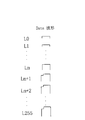
- FIG. 2 is a schematic diagram of a driving method of a liquid crystal panel according to an embodiment of the present invention.
- Figure 3 is an enlarged schematic view of a Date waveform of Figure 2.
- FIG. 4 is a schematic diagram of a driving method of a liquid crystal panel according to an embodiment of the present invention.
- Figure 5 is an enlarged schematic view of a Date waveform of Figure 4.
- FIG. 6 is a schematic diagram of a driving method of a liquid crystal panel according to another embodiment of the present invention.
- the present invention relates to a method for driving a liquid crystal panel.
- the liquid crystal panel includes a plurality of rows of gate lines and a plurality of rows of data lines.
- the gate lines and the data lines are perpendicularly intersected with each other to form a plurality of pixels distributed in an array.
- the row gate lines are arranged in parallel with each other along the first direction, and the plurality of rows of data lines are arranged in parallel with each other along the second direction, the first direction is perpendicular to the second direction, and the extending direction of the gate lines is regarded as the row direction, and the data lines are extended.
- the direction is treated as the column direction.
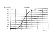
- Figure 1 shows the VT Curve of the actual product measurement of a liquid crystal panel.
- the saturation voltage is 4.5V.
- the driving voltage is changed, and the panel is pressed with a finger. It is found that when the driving voltage is lowered to 3.5V.
- the Trace mura phenomenon disappears within 2 seconds. In order to meet the specifications that Trace mura disappears within 2 seconds, it is necessary to reduce the maximum driving voltage from 4.5V to 3.5V, which is so serious.
- the transmittance of the liquid crystal display panel is lowered, and the brightness of the panel is lowered.
- the driving method of the liquid crystal panel of the present invention includes: when the gray scale value of the liquid crystal panel is smaller than the first gray scale, driving the data line by using a first driving voltage, wherein the first driving voltage is a corresponding corresponding gray The value of the normal drive voltage.
- the specific definition of the first driving voltage in the first gray-scale state is based on: when the finger presses the liquid crystal panel, the Trace mura phenomenon of the liquid crystal panel disappears within a prescribed time, and the liquid crystal panel is deemed to meet the requirements.
- the time is the time set by the user for the LCD panel, for example, 2 seconds. Different users have different rules for the disappearance of the Trace mura phenomenon after the finger pressure of the LCD panel.
- the first driving voltage is used, the Trace mura phenomenon can be specified.
- the grayscale value in this case is the first grayscale.
- the driving of the data line includes a first phase and a second phase, and the first phase is before the second phase
- the first stage is: driving the liquid crystal panel by using a second driving voltage
- the second driving voltage is less than or equal to the first driving voltage
- the second stage is: driving the liquid crystal panel by using a third driving voltage
- the third driving voltage is a normally driven voltage corresponding to a corresponding grayscale value.
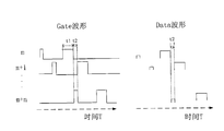
- FIG. 2 includes a Date waveform
- FIG. 3 is an enlarged schematic view of a Date waveform in FIG.
- the gray scale value of the liquid crystal panel shown in FIG. 2 is from L0 to L255.
- the L0 to Lm gray scale is driven by the corresponding normal driving voltage, and the Trace mura phenomenon does not occur after the liquid crystal panel is pressed in the L0 to Lm gray scale.
- L255 is driven by the saturation voltage, and the Trace mura phenomenon occurs after the finger presses the liquid crystal panel in the gray scale of Lm to L255. Therefore, the driving method of the present invention divides the data waveform of Lm to L255 into the first stage and the second stage, that is, the driving of the data line.
- the second driving voltage employed in the first stage is 0.5 to 1.3 V smaller than the third driving voltage of the second stage, and the third driving voltage may be a saturation voltage.
- the first stage is to drive the liquid crystal panel with a voltage lower than the normal driving voltage of the corresponding gray scale value.
- the liquid crystal molecules are in a standing state, and the lower voltage is favorable for the liquid crystal molecules to recover. This eliminates trace mura, which is a phenomenon of poor finger pressure.
- the second stage uses a third driving voltage, which can be close to or equal to the saturation voltage, and can improve the transmittance of the liquid crystal display panel.
- an intermediate phase is further included between the first phase and the second phase.
- the inter-stage is: applying a fourth driving voltage, the fourth driving voltage being greater than the third driving voltage and less than a saturation voltage for increasing the response speed of the liquid crystal panel. That is to say, after a lower voltage is applied to return the liquid crystal molecules to the flat surface, a voltage value of a normal driving voltage higher than the corresponding gray scale value is applied to drive the liquid crystal panel, in order to improve the response of the liquid crystal panel. time.
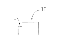
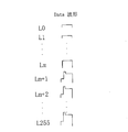
- FIG. 4 includes a Date waveform
- FIG. 5 is an enlarged schematic view of a Date waveform in FIG.
- the L0 to Lm gray scale is driven by the corresponding normal driving voltage, and the Trace mura phenomenon does not occur after the liquid crystal panel is pressed in the L0 to Lm gray scale.
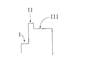
- the Trace mura phenomenon occurs after the finger presses the LCD panel in the Lm to L255 gray scale, and the data waveform of Lm to L255 is divided into three stages.
- the first stage (shown as I in Fig. 5) is to eliminate the low voltage of the trace mura.
- the phase shown as II in FIG.
- phase 5 is an over driver phase, that is, a fourth driving voltage is applied, and the fourth driving voltage is greater than the third driving voltage and less than a saturation voltage for boosting the response speed of the liquid crystal panel.
- the purpose of the phase is to increase the response speed of the LC, and the second phase (denoted as III in Figure 5) is the normal charging phase.
- the first phase, the intermediate phase, and the second phase occur sequentially in succession. In other words, there is no time interval between the three phases.
- the driving method does not include an intermediate stage, only the first stage and the second stage, the first stage and the second stage occurring continuously.
- the switch of the gate line of the mth row is turned on for a first time period, and the gray level corresponding to the gate line of the mth row is in the first time period.
- Charging the normal driving voltage of the value then turning off the gate switch of the mth row, turning on the switch of the gate line of the m+nth row for a second period of time, during the second period of time,
- the gate line of the m+nth row is charged with the second driving voltage, and both m and n are natural numbers greater than or equal to 1.
- the first time period and the second time period are continuous. After the second time period ends, the gate line of the m+1th row is charged, and the gate line of the m+1th row is used.
- the normal driving voltage of the corresponding grayscale value The charging time of the gate line of the m+1th row is the same as the time of the first time period. After charging the gate line of the m+1th row, the gate line of the m+1+nth row is The second driving voltage is charged, and the time for charging the gate line of the m+1+nth row is the same as the time of the second time period. Next, the above driving method is cyclically performed. The second driving voltage is lower than the normal driving voltage of the corresponding gray line value of the gate line. With such a lower voltage, the liquid crystal molecules are quickly restored to the flat state, and the trace mura is eliminated. Poor finger pressure.
- FIG. 6 shows gate lines (Gate waveforms) and data lines (Data waveforms) from the mth to m+nth rows, and the horizontal axis represents the time T.
- Each row gate open time t1 does not immediately supply the next row of charge after the charge is turned off, but leaves a period of time t2 to perform a low potential charge on a subsequent row to eliminate the occurrence of trace mura.
- the purpose of pre-charging is to supply the m+n line with a lower potential for the liquid crystal standing after the finger is pressed to return to the flat state.
- the lower voltage and the normal voltage according to the present invention are voltages corresponding to corresponding gray scale values, and the higher the gray scale value, the larger the normal driving voltage required. Therefore, when the grayscale value is small, two stages of charging are not required, and only the corresponding normal voltage is driven, and the trace mura phenomenon does not occur. When the grayscale value is large, if it is driven by its normal voltage, the trace mura phenomenon will occur. Therefore, two stages of driving are required. First, the lower voltage is used to eliminate the trace mura phenomenon and then apply the normal voltage. .
- the invention adopts two stages of driving voltage charging, including the first stage and the second, when the gray scale value of the liquid crystal panel is greater than the first gray level and less than the maximum gray level, that is, in the high gray level stage.
- Phase before the second phase, the first phase is: driving the liquid crystal panel with a second driving voltage, the second driving voltage is less than or equal to the first driving voltage, and the second phase is Driving the liquid crystal panel with a third driving voltage, which is a normal driving voltage corresponding to a corresponding gray scale value.
- the third driving voltage of the second stage is higher, and the saturation voltage can be approached, which can improve the transmittance of the liquid crystal display panel.
Landscapes
- Engineering & Computer Science (AREA)
- Theoretical Computer Science (AREA)
- Physics & Mathematics (AREA)
- General Physics & Mathematics (AREA)
- Computer Hardware Design (AREA)
- General Engineering & Computer Science (AREA)
- Chemical & Material Sciences (AREA)
- Crystallography & Structural Chemistry (AREA)
- Human Computer Interaction (AREA)
- Control Of Indicators Other Than Cathode Ray Tubes (AREA)
- Liquid Crystal (AREA)
Abstract
L'invention concerne un procédé de commande de panneau à cristaux liquides, comprenant les étapes suivantes : lorsqu'une valeur d'échelle de gris du panneau à cristaux liquides est inférieure à une première valeur d'échelle de gris, utilisation d'une première tension de commande pour commander une ligne de données, la première tension de commande étant une tension de commande normale correspondant à une valeur d'échelle de gris respective ; lorsque la valeur d'échelle de gris du panneau à cristaux liquides devient supérieure à la première échelle de gris et est inférieure ou égale à une échelle de gris maximale, la ligne de données est commandée par un premier étage (I) et un deuxième étage (II), le premier étage (I) précédant le deuxième étage (II) ; le premier étage (I) utilise une deuxième tension de commande pour commander le panneau à cristaux liquides, la deuxième tension de commande étant inférieure ou égale à la première tension de commande ; le deuxième étage (II) utilise une troisième tension de commande pour commander le panneau à cristaux liquides, la troisième tension de commande étant la tension de commande normale correspondant à une échelle de gris respective. Le procédé aborde le problème d'une faible pression du doigt et améliore les performances d'un panneau à cristaux liquides.
Priority Applications (1)
| Application Number | Priority Date | Filing Date | Title |
|---|---|---|---|
| US14/435,517 US9766740B2 (en) | 2014-12-31 | 2015-01-21 | Method for driving liquid crystal panel |
Applications Claiming Priority (2)
| Application Number | Priority Date | Filing Date | Title |
|---|---|---|---|
| CN201410854121.2 | 2014-12-31 | ||
| CN201410854121.2A CN104575423B (zh) | 2014-12-31 | 2014-12-31 | 液晶面板的驱动方法 |
Publications (1)
| Publication Number | Publication Date |
|---|---|
| WO2016106902A1 true WO2016106902A1 (fr) | 2016-07-07 |
Family
ID=53091337
Family Applications (1)
| Application Number | Title | Priority Date | Filing Date |
|---|---|---|---|
| PCT/CN2015/071216 Ceased WO2016106902A1 (fr) | 2014-12-31 | 2015-01-21 | Procédé de commande d'un panneau à cristaux liquides |
Country Status (3)
| Country | Link |
|---|---|
| US (1) | US9766740B2 (fr) |
| CN (1) | CN104575423B (fr) |
| WO (1) | WO2016106902A1 (fr) |
Families Citing this family (4)
| Publication number | Priority date | Publication date | Assignee | Title |
|---|---|---|---|---|
| CN112130360A (zh) * | 2020-09-29 | 2020-12-25 | 厦门天马微电子有限公司 | 显示面板、显示装置及显示方法 |
| CN113066415B (zh) * | 2021-03-01 | 2023-01-24 | 惠科股份有限公司 | 显示面板充电方法、装置以及显示终端 |
| KR20220136539A (ko) * | 2021-03-30 | 2022-10-11 | 삼성디스플레이 주식회사 | 표시 장치 및 입력 센서를 이용한 근접 신호 센싱 방법 |
| CN114787904B (zh) * | 2021-12-07 | 2025-06-13 | 惠州华星光电显示有限公司 | 显示器的驱动方法及显示器 |
Citations (9)
| Publication number | Priority date | Publication date | Assignee | Title |
|---|---|---|---|---|
| US20030122758A1 (en) * | 2001-12-27 | 2003-07-03 | Nam-Seok Lee | Method of driving cholesteric liquid crystal display panel for accurate gray-scale display |
| CN1530909A (zh) * | 2003-03-12 | 2004-09-22 | ������������ʽ���� | 显示装置 |
| CN101140749A (zh) * | 2007-10-31 | 2008-03-12 | 友达光电股份有限公司 | 像素的驱动方法 |
| US20120182280A1 (en) * | 2011-01-14 | 2012-07-19 | Jin-O Park | Gamma voltage generating device, LCD device, and method of driving the LCD device |
| CN102855856A (zh) * | 2012-08-30 | 2013-01-02 | 南京中电熊猫液晶显示科技有限公司 | 一种消除液晶显示器Mura的驱动方法及其液晶显示器 |
| CN103035196A (zh) * | 2011-10-04 | 2013-04-10 | 乐金显示有限公司 | 有机发光显示设备 |
| TW201405534A (zh) * | 2012-06-08 | 2014-02-01 | Apple Inc | 使用對比度增強成像以減少或去除斑紋假影之系統及方法 |
| CN103943077A (zh) * | 2013-12-03 | 2014-07-23 | 厦门天马微电子有限公司 | 一种显示装置驱动电压的调节方法及显示装置 |
| US20140368562A1 (en) * | 2013-06-13 | 2014-12-18 | Samsung Display Co., Ltd. | Display device having improved contrast ratio |
Family Cites Families (4)
| Publication number | Priority date | Publication date | Assignee | Title |
|---|---|---|---|---|
| JP2001318658A (ja) * | 2000-03-02 | 2001-11-16 | Sharp Corp | 液晶表示装置 |
| JP2004317785A (ja) * | 2003-04-16 | 2004-11-11 | Seiko Epson Corp | 電気光学装置の駆動方法、電気光学装置および電子機器 |
| KR20120049022A (ko) * | 2010-11-08 | 2012-05-16 | 삼성모바일디스플레이주식회사 | 액정 표시 장치 및 그의 구동 방법 |
| CN102890916B (zh) * | 2011-07-18 | 2015-05-13 | 财团法人工业技术研究院 | 多重稳态显示器的驱动方法 |
-
2014
- 2014-12-31 CN CN201410854121.2A patent/CN104575423B/zh active Active
-
2015
- 2015-01-21 US US14/435,517 patent/US9766740B2/en active Active
- 2015-01-21 WO PCT/CN2015/071216 patent/WO2016106902A1/fr not_active Ceased
Patent Citations (9)
| Publication number | Priority date | Publication date | Assignee | Title |
|---|---|---|---|---|
| US20030122758A1 (en) * | 2001-12-27 | 2003-07-03 | Nam-Seok Lee | Method of driving cholesteric liquid crystal display panel for accurate gray-scale display |
| CN1530909A (zh) * | 2003-03-12 | 2004-09-22 | ������������ʽ���� | 显示装置 |
| CN101140749A (zh) * | 2007-10-31 | 2008-03-12 | 友达光电股份有限公司 | 像素的驱动方法 |
| US20120182280A1 (en) * | 2011-01-14 | 2012-07-19 | Jin-O Park | Gamma voltage generating device, LCD device, and method of driving the LCD device |
| CN103035196A (zh) * | 2011-10-04 | 2013-04-10 | 乐金显示有限公司 | 有机发光显示设备 |
| TW201405534A (zh) * | 2012-06-08 | 2014-02-01 | Apple Inc | 使用對比度增強成像以減少或去除斑紋假影之系統及方法 |
| CN102855856A (zh) * | 2012-08-30 | 2013-01-02 | 南京中电熊猫液晶显示科技有限公司 | 一种消除液晶显示器Mura的驱动方法及其液晶显示器 |
| US20140368562A1 (en) * | 2013-06-13 | 2014-12-18 | Samsung Display Co., Ltd. | Display device having improved contrast ratio |
| CN103943077A (zh) * | 2013-12-03 | 2014-07-23 | 厦门天马微电子有限公司 | 一种显示装置驱动电压的调节方法及显示装置 |
Also Published As
| Publication number | Publication date |
|---|---|
| CN104575423B (zh) | 2017-07-28 |
| US20160342261A1 (en) | 2016-11-24 |
| US9766740B2 (en) | 2017-09-19 |
| CN104575423A (zh) | 2015-04-29 |
Similar Documents
| Publication | Publication Date | Title |
|---|---|---|
| CN103460122B (zh) | 液晶显示面板和液晶显示装置 | |
| JP5719439B2 (ja) | 液晶駆動装置及び液晶表示装置 | |
| US10510308B2 (en) | Display device with each column of sub-pixel units being driven by two data lines and driving method for display device | |
| TWI638347B (zh) | 整合觸控感測器之液晶顯示裝置 | |
| JP6334114B2 (ja) | 表示装置 | |
| US20070285369A1 (en) | Liquid crystal display device and driving method | |
| KR102091434B1 (ko) | 표시 장치 | |
| US9171516B2 (en) | Gate driver on array circuit | |
| CN104182108A (zh) | 阵列基板、触控显示装置及驱动方法 | |
| CN103529573B (zh) | 驱动双模式液晶显示装置的方法 | |
| WO2016106902A1 (fr) | Procédé de commande d'un panneau à cristaux liquides | |
| WO2012128061A1 (fr) | Procédé de commande de cristaux liquides et dispositif d'affichage à cristaux liquides | |
| US20200105212A1 (en) | Display device including data line alternately connected to adjacent pixel columns | |
| CN103488014A (zh) | 液晶面板的像素结构、显示装置及过压驱动方法 | |
| US20180068624A1 (en) | Content-based vcom driving | |
| CN102692772B (zh) | 液晶显示装置以及驱动液晶显示装置的方法 | |
| US9704889B2 (en) | Display panel and display device comprising the same | |
| TWI426496B (zh) | 無上板電極之液晶顯示裝置 | |
| CN115985260A (zh) | 显示装置的控制方法和显示装置 | |
| US8723852B2 (en) | Method of driving a display panel, and display device for performing the method | |
| US9311871B2 (en) | Devices and methods for reducing power to drive pixels of a display | |
| CN104267551A (zh) | 一种阵列基板、显示面板及显示装置 | |
| CN101853635B (zh) | 显示器驱动方法 | |
| US20120242711A1 (en) | Display device and method of driving a display panel | |
| JP2006065330A (ja) | Ocbモード液晶表示装置及びその駆動方法 |
Legal Events
| Date | Code | Title | Description |
|---|---|---|---|
| WWE | Wipo information: entry into national phase |
Ref document number: 14435517 Country of ref document: US |
|
| 121 | Ep: the epo has been informed by wipo that ep was designated in this application |
Ref document number: 15874595 Country of ref document: EP Kind code of ref document: A1 |
|
| NENP | Non-entry into the national phase |
Ref country code: DE |
|
| 122 | Ep: pct application non-entry in european phase |
Ref document number: 15874595 Country of ref document: EP Kind code of ref document: A1 |