WO2016074310A1 - 曲面液晶显示面板及曲面液晶显示装置 - Google Patents
曲面液晶显示面板及曲面液晶显示装置 Download PDFInfo
- Publication number
- WO2016074310A1 WO2016074310A1 PCT/CN2014/093909 CN2014093909W WO2016074310A1 WO 2016074310 A1 WO2016074310 A1 WO 2016074310A1 CN 2014093909 W CN2014093909 W CN 2014093909W WO 2016074310 A1 WO2016074310 A1 WO 2016074310A1
- Authority
- WO
- WIPO (PCT)
- Prior art keywords
- liquid crystal
- crystal display
- color
- display panel
- curved liquid
- Prior art date
- Legal status (The legal status is an assumption and is not a legal conclusion. Google has not performed a legal analysis and makes no representation as to the accuracy of the status listed.)
- Ceased
Links
Classifications
-
- G—PHYSICS
- G02—OPTICS
- G02F—OPTICAL DEVICES OR ARRANGEMENTS FOR THE CONTROL OF LIGHT BY MODIFICATION OF THE OPTICAL PROPERTIES OF THE MEDIA OF THE ELEMENTS INVOLVED THEREIN; NON-LINEAR OPTICS; FREQUENCY-CHANGING OF LIGHT; OPTICAL LOGIC ELEMENTS; OPTICAL ANALOGUE/DIGITAL CONVERTERS
- G02F1/00—Devices or arrangements for the control of the intensity, colour, phase, polarisation or direction of light arriving from an independent light source, e.g. switching, gating or modulating; Non-linear optics
- G02F1/01—Devices or arrangements for the control of the intensity, colour, phase, polarisation or direction of light arriving from an independent light source, e.g. switching, gating or modulating; Non-linear optics for the control of the intensity, phase, polarisation or colour
- G02F1/13—Devices or arrangements for the control of the intensity, colour, phase, polarisation or direction of light arriving from an independent light source, e.g. switching, gating or modulating; Non-linear optics for the control of the intensity, phase, polarisation or colour based on liquid crystals, e.g. single liquid crystal display cells
- G02F1/133—Constructional arrangements; Operation of liquid crystal cells; Circuit arrangements
- G02F1/1333—Constructional arrangements; Manufacturing methods
- G02F1/1335—Structural association of cells with optical devices, e.g. polarisers or reflectors
- G02F1/133509—Filters, e.g. light shielding masks
- G02F1/133512—Light shielding layers, e.g. black matrix
-
- G—PHYSICS
- G02—OPTICS
- G02F—OPTICAL DEVICES OR ARRANGEMENTS FOR THE CONTROL OF LIGHT BY MODIFICATION OF THE OPTICAL PROPERTIES OF THE MEDIA OF THE ELEMENTS INVOLVED THEREIN; NON-LINEAR OPTICS; FREQUENCY-CHANGING OF LIGHT; OPTICAL LOGIC ELEMENTS; OPTICAL ANALOGUE/DIGITAL CONVERTERS
- G02F1/00—Devices or arrangements for the control of the intensity, colour, phase, polarisation or direction of light arriving from an independent light source, e.g. switching, gating or modulating; Non-linear optics
- G02F1/01—Devices or arrangements for the control of the intensity, colour, phase, polarisation or direction of light arriving from an independent light source, e.g. switching, gating or modulating; Non-linear optics for the control of the intensity, phase, polarisation or colour
- G02F1/13—Devices or arrangements for the control of the intensity, colour, phase, polarisation or direction of light arriving from an independent light source, e.g. switching, gating or modulating; Non-linear optics for the control of the intensity, phase, polarisation or colour based on liquid crystals, e.g. single liquid crystal display cells
- G02F1/133—Constructional arrangements; Operation of liquid crystal cells; Circuit arrangements
- G02F1/1333—Constructional arrangements; Manufacturing methods
- G02F1/1335—Structural association of cells with optical devices, e.g. polarisers or reflectors
- G02F1/133509—Filters, e.g. light shielding masks
- G02F1/133514—Colour filters
-
- G—PHYSICS
- G02—OPTICS
- G02F—OPTICAL DEVICES OR ARRANGEMENTS FOR THE CONTROL OF LIGHT BY MODIFICATION OF THE OPTICAL PROPERTIES OF THE MEDIA OF THE ELEMENTS INVOLVED THEREIN; NON-LINEAR OPTICS; FREQUENCY-CHANGING OF LIGHT; OPTICAL LOGIC ELEMENTS; OPTICAL ANALOGUE/DIGITAL CONVERTERS
- G02F1/00—Devices or arrangements for the control of the intensity, colour, phase, polarisation or direction of light arriving from an independent light source, e.g. switching, gating or modulating; Non-linear optics
- G02F1/01—Devices or arrangements for the control of the intensity, colour, phase, polarisation or direction of light arriving from an independent light source, e.g. switching, gating or modulating; Non-linear optics for the control of the intensity, phase, polarisation or colour
- G02F1/13—Devices or arrangements for the control of the intensity, colour, phase, polarisation or direction of light arriving from an independent light source, e.g. switching, gating or modulating; Non-linear optics for the control of the intensity, phase, polarisation or colour based on liquid crystals, e.g. single liquid crystal display cells
- G02F1/133—Constructional arrangements; Operation of liquid crystal cells; Circuit arrangements
- G02F1/1333—Constructional arrangements; Manufacturing methods
- G02F1/1343—Electrodes
-
- G—PHYSICS
- G02—OPTICS
- G02F—OPTICAL DEVICES OR ARRANGEMENTS FOR THE CONTROL OF LIGHT BY MODIFICATION OF THE OPTICAL PROPERTIES OF THE MEDIA OF THE ELEMENTS INVOLVED THEREIN; NON-LINEAR OPTICS; FREQUENCY-CHANGING OF LIGHT; OPTICAL LOGIC ELEMENTS; OPTICAL ANALOGUE/DIGITAL CONVERTERS
- G02F1/00—Devices or arrangements for the control of the intensity, colour, phase, polarisation or direction of light arriving from an independent light source, e.g. switching, gating or modulating; Non-linear optics
- G02F1/01—Devices or arrangements for the control of the intensity, colour, phase, polarisation or direction of light arriving from an independent light source, e.g. switching, gating or modulating; Non-linear optics for the control of the intensity, phase, polarisation or colour
- G02F1/13—Devices or arrangements for the control of the intensity, colour, phase, polarisation or direction of light arriving from an independent light source, e.g. switching, gating or modulating; Non-linear optics for the control of the intensity, phase, polarisation or colour based on liquid crystals, e.g. single liquid crystal display cells
- G02F1/133—Constructional arrangements; Operation of liquid crystal cells; Circuit arrangements
- G02F1/1333—Constructional arrangements; Manufacturing methods
- G02F1/1343—Electrodes
- G02F1/134309—Electrodes characterised by their geometrical arrangement
-
- G—PHYSICS
- G02—OPTICS
- G02F—OPTICAL DEVICES OR ARRANGEMENTS FOR THE CONTROL OF LIGHT BY MODIFICATION OF THE OPTICAL PROPERTIES OF THE MEDIA OF THE ELEMENTS INVOLVED THEREIN; NON-LINEAR OPTICS; FREQUENCY-CHANGING OF LIGHT; OPTICAL LOGIC ELEMENTS; OPTICAL ANALOGUE/DIGITAL CONVERTERS
- G02F1/00—Devices or arrangements for the control of the intensity, colour, phase, polarisation or direction of light arriving from an independent light source, e.g. switching, gating or modulating; Non-linear optics
- G02F1/01—Devices or arrangements for the control of the intensity, colour, phase, polarisation or direction of light arriving from an independent light source, e.g. switching, gating or modulating; Non-linear optics for the control of the intensity, phase, polarisation or colour
- G02F1/13—Devices or arrangements for the control of the intensity, colour, phase, polarisation or direction of light arriving from an independent light source, e.g. switching, gating or modulating; Non-linear optics for the control of the intensity, phase, polarisation or colour based on liquid crystals, e.g. single liquid crystal display cells
- G02F1/133—Constructional arrangements; Operation of liquid crystal cells; Circuit arrangements
- G02F1/1333—Constructional arrangements; Manufacturing methods
- G02F1/1343—Electrodes
- G02F1/134309—Electrodes characterised by their geometrical arrangement
- G02F1/134336—Matrix
Definitions
- the present invention relates to the field of displays, and in particular to a curved liquid crystal display panel and a curved liquid crystal display device.
- Liquid crystal display (Liquid Crystal Display, LCD) has been widely used in a variety of electronic products, most of which are backlit LCDs, including liquid crystal display panels and backlight modules (backlight Module).
- the backlight module can be divided into a side-light type and a direct-light type according to the incident position of the light source (Direct-light) Type) Two to provide a backlight to the LCD panel.
- Direct-light Direct-light
- FIG. 1 is a schematic structural view of a conventional side-lit backlight module, wherein 101 is a light guide plate, 102 is a light source, and 103 is a specular reflection sheet, and the light emitted by the light source 102 in the figure is The energy is concentrated directly above the light source 102. Most of the light A needs to be reflected by the specular reflection sheet 103 to enter the inside of the light guide plate 101, and a part of the light B is reflected by the specular reflection sheet 103 and returns to the light source 102. Part of the light cannot enter the light guide plate 101, thereby affecting the light coupling efficiency of the backlight module. Therefore, the lateral backlight module with the light entering the bottom side has a lower energy utilization ratio of 12% to 15 than the conventional side light input side backlight module. %.
- An object of the present invention is to provide a curved liquid crystal display panel and a curved liquid crystal display device, which can prevent the occurrence of color shift by matching the curved direction of the curved liquid crystal display panel with the extending direction of the long side of the pixel electrode;
- the curved liquid crystal display panel and the curved liquid crystal display device are susceptible to color shift or light leakage due to the relative offset between the color filter substrate and the array substrate, thereby affecting the technical quality of the liquid crystal display device.
- Embodiments of the present invention provide a curved liquid crystal display panel, including:
- a color film substrate provided with a color film color resistance and a black matrix
- the array substrate is disposed opposite to the color filter substrate, and is provided with a pixel electrode and a data line, wherein the pixel electrode has a first side and a second side, wherein a side length of the first side is greater than a second side a side length; wherein the curved liquid crystal display panel has a same bending direction as the first side; and
- liquid crystal layer disposed between the color film substrate and the array substrate;
- the curved liquid crystal display panel includes a left side area, a middle area, and a right side area; the black matrix is widened according to a bending offset, and the black matrix has a widening value equal to the bending offset a value to eliminate the color shift of the curved liquid crystal display panel, the bending offset being an offset between the color film color resistance and the corresponding pixel electrode.
- the bending offset is obtained according to the thickness of the color filter substrate, the elastic modulus of the color filter substrate, and the radius of curvature of the color filter substrate.
- the bending offset is:
- K is the bending offset
- E is the elastic modulus of the color filter substrate
- P is atmospheric pressure
- r is the radius of curvature of the color filter substrate
- d is the thickness of the color filter substrate.
- the black matrix of the left side region and the right side region is subjected to a widening process according to the bending offset amount.
- the color film color resistance on the color film substrate on the left side region is shifted to the left relative to the corresponding pixel electrode on the array substrate, and is located on the right side.
- the color film color resistance of the color filter substrate in the side region is shifted to the right with respect to the corresponding pixel electrode on the array substrate.
- the color film color resistance includes a red color film, a green color film, and a blue color film.
- the pixel electrode and the color film color resistance are oppositely disposed.
- Embodiments of the present invention provide a curved liquid crystal display panel, including:
- a color film substrate provided with a color film color resistance and a black matrix
- the array substrate is disposed opposite to the color filter substrate, and is provided with a pixel electrode and a data line, wherein the pixel electrode has a first side and a second side, wherein a side length of the first side is greater than a second side a side length; wherein the curved liquid crystal display panel has a same bending direction as the first side; and
- the liquid crystal layer is disposed between the color film substrate and the array substrate.
- the black matrix is subjected to a widening process according to a bending offset, and a widening value of the black matrix is equal to a value of the bending offset to eliminate the The color shift of the curved liquid crystal display panel, wherein the bending offset is an offset between the color film color resistance and the corresponding pixel electrode.
- the bending offset is obtained according to the thickness of the color filter substrate, the elastic modulus of the color filter substrate, and the radius of curvature of the color filter substrate.
- the bending offset is:
- K is the bending offset
- E is the elastic modulus of the color filter substrate
- P is atmospheric pressure
- r is the radius of curvature of the color filter substrate
- d is the thickness of the color filter substrate.
- the curved liquid crystal display panel of the present invention includes a left side area, an intermediate area, and a right side area, and the left side area and the right side area are according to the bending offset amount.
- the black matrix is subjected to a widening process.
- the present invention also provides a curved liquid crystal display device, the device comprising a backlight module and a curved liquid crystal display panel, the curved liquid crystal display panel comprising:
- a color film substrate provided with a color film color resistance and a black matrix
- the array substrate is disposed opposite to the color filter substrate, and is provided with a pixel electrode and a data line, wherein the pixel electrode has a first side and a second side, wherein a side length of the first side is greater than a second side a side length; wherein the curved liquid crystal display panel has a same bending direction as the first side; and
- the liquid crystal layer is disposed between the color film substrate and the array substrate.
- the black matrix is subjected to a widening process according to a bending offset, and a widening value of the black matrix is equal to a value of the bending offset to eliminate the The color shift of the curved liquid crystal display panel, wherein the bending offset is an offset between the color film color resistance and the corresponding pixel electrode.
- the bending offset amount is obtained according to the thickness of the color filter substrate, the elastic modulus of the color filter substrate, and the radius of curvature of the color filter substrate.
- the bending offset is:
- K is the bending offset
- E is the elastic modulus of the color filter substrate
- P is atmospheric pressure
- r is the radius of curvature of the color filter substrate
- d is the thickness of the color filter substrate.
- the curved liquid crystal display panel includes a left side area, an intermediate area, and a right side area, and the left side area and the right side area are according to the bending offset amount.
- the black matrix is subjected to a widening process.
- the curved liquid crystal display panel and the curved liquid crystal display device of the present invention reduce the color shift by keeping the curved direction of the curved liquid crystal display panel and the extending direction of the long side of the pixel electrode, thereby solving the prior art due to the color film substrate and the array.
- the color shift or light leakage phenomenon caused by the relative offset between the substrates improves the display quality of the liquid crystal display device.
- FIG. 1 is a schematic structural view and a partial structural view of a conventional curved liquid crystal display device
- FIG. 2 is a schematic structural view and a partial structural view of a first preferred embodiment of a curved liquid crystal display panel of the present invention
- FIG. 3 is a schematic structural view and a partial structural view of a second preferred embodiment of a curved liquid crystal display panel of the present invention.
- FIG 4 is a front view of the small square body on the color filter substrate when the color filter substrate is divided into an infinite number of small cubes in the second preferred embodiment of the curved liquid crystal display panel of the present invention.
- Figure 5 is a force exploded view of the small cube in Figure 4.
- FIG. 6 is a schematic diagram of integration of a curved liquid crystal display panel of the present invention.
- FIG. 2 is a schematic structural view and a partial structural view of a first preferred embodiment of a curved liquid crystal display panel according to the present invention.
- the curved liquid crystal display panel of the preferred embodiment includes a color film substrate 21 having a curved surface structure, an array substrate 22 having a curved surface structure, and a liquid crystal layer disposed between the color filter substrate 21 and the array substrate 22.
- the specific structure of the color film substrate 21 and the array substrate 22 is as shown in the upper part of FIG. 2 .
- the color film substrate 21 is provided with a black matrix 212 and a color film color resist 211, and the color film color resistance may include a red color film R, a green color film G, and a blue color film B. It can also include a white color film and a yellow color film.
- the array substrate 22 is disposed opposite to the color filter substrate 21, and the array substrate 22 is provided with a pixel electrode 221, a data line 222, and a scan line (not shown).
- the pixel electrode 221 of the array substrate 22 is opposite to the color filter 211 of the color filter substrate 21 (ie, one-to-one correspondence); thus, each pixel can emit red through the color filter substrate 21. , green, blue three-color light.
- the color film 211 on both sides of the color filter substrate 21 corresponds to the array substrate 22 as shown in the lower part of FIG.
- the pixel electrode 221 is shifted.
- the color film color resist 211 of the color filter substrate 21 on the left side of the curved liquid crystal display panel is shifted to the left relative to the corresponding pixel electrode 221 on the array substrate 22, and the color film substrate 21 on the right side of the curved liquid crystal display panel is colored.
- the film color resist 211 is shifted to the right with respect to the corresponding pixel electrode 221 on the array substrate 22.
- the pixel electrode 221 of the curved liquid crystal display panel of the preferred embodiment has a first side 31 (long side) and a second side 32 (short side), wherein the first side The side length of the third side 32 is larger than the side length of the second side 32.
- the curved liquid crystal display panel of the present invention has the same bending direction as the first side 31, and the liquid crystal display panel of the planar structure is along the pixel electrode. The long side direction is curved to form a curved liquid crystal display panel.
- the curved direction of the curved liquid crystal display panel is also the same as the longitudinal direction of the color film color resistance.
- the liquid crystal display panel of the planar structure is curved along the short side direction of the pixel electrode, and the present embodiment adopts the above-mentioned bending manner to separate the BM between pixels in a unit area.
- Reduction that is, the ratio of the width m1 of the black matrix between the two color film color resists to the width m2 of the color film color resistance between the two black matrices is reduced (while the prior art m2 is the color film resistive short side Side length), when the color film color resistance of the color film substrate is offset from the corresponding pixel electrode, the offset K1 between the pixel electrode and the color film color resistance can be reduced, thereby reducing the color resistance due to the pixel electrode and the color film. Defects such as color shift and light leakage caused by offset.
- the color shift is reduced, and light leakage is avoided.
- FIG. 3 is a schematic structural view and a partial structural view of a second preferred embodiment of the curved liquid crystal display panel of the present invention.
- the curved liquid crystal display panel of the preferred embodiment includes a color film substrate 41 having a curved surface structure, an array substrate 42 having a curved surface structure, and a liquid crystal layer disposed between the color filter substrate 41 and the array substrate 42.
- the specific structure of the color film substrate 41 and the array substrate 42 is as shown in the upper part of FIG.
- the color film substrate 41 is provided with a black matrix 412 and a color film color resistance 411, and the color film color resistance may include a red color film R, a green color film G, and a blue color film B.
- the array substrate 42 is disposed opposite to the color filter substrate 41, and is provided with a pixel electrode 421, a data line 422, and a scan line (not shown).
- the pixel electrode 421 of the array substrate 42 is opposite to the color film color 411 of the color filter substrate 41 (ie, one-to-one correspondence); thus, each pixel can emit red and green through the color filter substrate 41. , blue three-color light.
- the pixel electrode 421 has an offset phenomenon.
- the color filter 411 of the color filter substrate 41 on the left side of the curved liquid crystal display panel is shifted to the left with respect to the corresponding pixel electrode 421, and the color film 411 of the color filter substrate 41 located on the right side of the curved liquid crystal display panel is relatively corresponding.
- the pixel electrode 421 is shifted to the right.
- the curved liquid crystal display panel of the present invention may have the same direction of extension as the long side 51 of the pixel electrode 221, or may be aligned with the short side 52 of the pixel electrode, that is, the liquid crystal display panel of the planar structure may be along the pixel.
- the long side or the short side of the electrode is bent to form a curved liquid crystal display panel.
- the offset amount K2 between the color film color resist 411 and the corresponding pixel electrode 411 is referred to as a bending offset, and the derivation process of the bending offset is given below:
- the color film substrate of the curved surface has a semi-annular structure, as shown in FIG. 4, the color film substrate of the half ring structure is divided into an infinite number of small cubes, wherein the broken line portion represents a front view of one of the small cubes divided into
- the pressure of the color film substrate is expressed by formula (1):
- P is the pressure of the atmosphere, usually taking the standard atmospheric pressure
- F is the pressure received by the color film substrate
- S is the force receiving area
- a small square body force exploded view of FIG. 4 is given.
- the small square body is subjected to forces in three directions (a, b, and c), a represents a curved direction of the curved liquid crystal display panel, and b represents a curved surface.
- the tangential direction of the bending direction of the liquid crystal display panel, and c indicates the direction in which the paper faces outward.
- Indicates the pressure applied to the unit area of the small cube in the a direction indicating the pressure applied to the unit area of the small cube in the b direction.
- the pressure applied to the color film substrate can be divided into a force Fn applied to both sides and a force F in the middle.
- y in general, the middle of the color film substrate is unstressed, so Equation 2 is obtained:
- the pressure on each small cube is integrated by the curve integral principle to integrate the arc surface of the entire color film substrate to obtain the pressure of each small cube:
- Equation 5 is simplified as:
- the color film substrate is subjected to a total pressure of F0:
- the area Sb of the color filter substrate in the b direction is:
- K2 is the bending offset
- K2 is in meters
- E is the elastic modulus of the color filter substrate
- E is in units of MPa
- P is atmospheric
- P is in Pa
- P is taken The standard atmospheric pressure
- r the radius of curvature of the color filter substrate
- the unit of r is meters
- d is the thickness of the color filter substrate
- the unit of d is meters.
- the bending offset is obtained according to the thickness of the color filter substrate, the elastic modulus of the color filter substrate, and the radius of curvature of the color filter substrate, because when the liquid crystal display panel of the planar structure is bent, An offset occurs between the pixel electrode and the color film color resistance, and the black matrix (BM) is subjected to a widening process according to the bending offset amount K2, wherein the black matrix has a widened value equal to the bending offset amount K2 Value, by widening the black matrix method, so that the pixel electrode and the color film color resistance are one-to-one correspondence, eliminating the color shift problem of the curved liquid crystal display panel, and all the black matrix of the entire color film substrate can be Both are widened.
- the curved liquid crystal display panel includes a left side area, a middle area, and a right side area, and the offset may be caused only between the left side area and the right side area between the pixel electrode and the color film color resistance.
- the bending offset only widens the black matrix of the left side region and the right side region, wherein the black matrix has a widened value equal to the value of the bending offset.
- the width of the black matrix is larger than the width of the data line (in general, the width of the black matrix and the width of the data line are equal, and the black matrix is set relative to the data line), thereby avoiding
- the relative offset between the color filter substrate and the array substrate is further increased, and two adjacent color film color resists move to the vicinity of the data line, so that an electric field near the data line causes a liquid crystal to be deflected, resulting in an appearance.
- the curved liquid crystal display panel of the present invention by widening the black matrix, defects such as color shift and light leakage are eliminated.
- the present invention also provides a curved liquid crystal display device comprising a backlight module and a curved liquid crystal display panel, the backlight module comprising a light source and a light guide plate, the light source for providing outgoing light, and the light guide plate for transmitting the outgoing light To the curved LCD panel.
- the curved liquid crystal display panel comprises a color film substrate of a curved structure, an array substrate of a curved structure, and a liquid crystal layer, and the liquid crystal layer is disposed between the color film substrate and the array substrate.
- the color filter substrate is provided with a color film color resistance and a black matrix
- the array substrate is disposed opposite to the color filter substrate, and is provided with a pixel electrode and a data line, wherein the pixel electrode has a first side and a second side, wherein a side length of the first side is greater than the second side The side length of the side; wherein the curved liquid crystal display panel has the same bending direction as the first side.
- the curved liquid crystal display device of the present invention can adopt any of the above-mentioned curved liquid crystal display panels. Since the curved liquid crystal display panel has been described in detail above, it will not be described herein.
- the curved liquid crystal display device of the present invention reduces the color shift by keeping the curved direction of the curved liquid crystal display panel and the extending direction of the long side of the pixel electrode, thereby avoiding light leakage or widening the black matrix. Processing, thereby eliminating the phenomenon of color shift, light leakage and the like.
Landscapes
- Physics & Mathematics (AREA)
- Nonlinear Science (AREA)
- Mathematical Physics (AREA)
- Chemical & Material Sciences (AREA)
- Crystallography & Structural Chemistry (AREA)
- General Physics & Mathematics (AREA)
- Optics & Photonics (AREA)
- Geometry (AREA)
- Liquid Crystal (AREA)
- Optical Filters (AREA)
- Devices For Indicating Variable Information By Combining Individual Elements (AREA)
Abstract
一种曲面液晶显示面板,其包括彩膜基板(21)、与彩膜基板(21)相对设置的阵列基板(22),阵列基板(22)上设置有像素电极(221),像素电极(221)具有第一边(31)和第二边(32),第一边(31)的边长大于第二边(32)的边长;曲面液晶显示面板的弯曲方向与第一边(31)的延伸方向相同。
Description
本发明涉及显示器领域,特别是涉及一种曲面液晶显示面板及曲面液晶显示装置。
液晶显示器(Liquid Crystal
Display,LCD)已被广泛应用于各种电子产品中,液晶显示器大部分为背光型液晶显示器,其包括液晶显示面板及背光模块(backlight
module)。背光模块可依照光源入射位置的不同分成侧向式入光(Side-light type)与直下式入光(Direct-light
type)两种,以便提供背光源至液晶显示面板。
如图1所示,图1为现有的底面入光的侧向式背光模块的结构示意图,其中101为导光板,102为光源,103为镜面反射片,图中的光源102发出的光的能量集中在光源102的正上方,大部分光线A需要经过镜面反射片103的反射后才能进入到导光板101的内部,还有一部分光线B经镜面反射片103反射后会回到光源102,这部分光无法进入到导光板101中,从而影响了背光模块的耦光效率,因此底面入光的侧向式背光模块较传统的侧面入光的侧向式背光模块能量利用率低12%至15%。
故,有必要提供一种背光模块以及液晶显示装置,以解决现有技术所存在的问题。
本发明的目的在于提供一种曲面液晶显示面板及曲面液晶显示装置,通过将曲面液晶显示面板的弯曲方向与像素电极的长边延伸方向保持一致,以避免色偏现象的产生;以解决现有的曲面液晶显示面板及曲面液晶显示装置由于彩膜基板和阵列基板之间的相对偏移,导致易产生色偏或者漏光现象,从而影响液晶显示装置的显示品质的技术问题。
。
本发明实施例提供一种曲面液晶显示面板,其包括:
彩膜基板,设置有彩膜色阻和黑色矩阵;
阵列基板,与所述彩膜基板相对设置,设置有像素电极和数据线,其中所述像素电极具有第一边和第二边,其中所述第一边的边长大于所述第二边的边长;其中所述曲面液晶显示面板的弯曲方向与所述第一边的延伸方向相同;以及
液晶层,设置于所述彩膜基板和所述阵列基板之间;
其中所述曲面液晶显示面板包括左侧区域、中间区域、右侧区域;根据弯曲偏移量对所述黑色矩阵进行加宽处理,且所述黑色矩阵的加宽值等于所述弯曲偏移量的值,以消除所述曲面液晶显示面板的色偏,所述弯曲偏移量为所述彩膜色阻与相应的像素电极之间的偏移量。
在本发明所述的曲面液晶显示面板中,根据所述彩膜基板的厚度、所述彩膜基板的弹性模量以及所述彩膜基板的曲率半径,获取所述弯曲偏移量。
在本发明所述的曲面液晶显示面板中,所述弯曲偏移量为:
K=E*P*r/(8*d);
其中,K为所述弯曲偏移量,E为所述彩膜基板的弹性模量、P为大气压强、r所述彩膜基板的曲率半径、d为所述彩膜基板的厚度。
在本发明所述的曲面液晶显示面板中,根据所述弯曲偏移量对所述左侧区域和所述右侧区域的所述黑色矩阵进行加宽处理。
在本发明所述的曲面液晶显示面板中,位于所述左侧区域的所述彩膜基板上的彩膜色阻相对所述阵列基板上相应的像素电极向左偏移,而位于所述右侧区域的所述彩膜基板的彩膜色阻相对所述阵列基板上相应的像素电极向右偏移。
在本发明所述的曲面液晶显示面板中,所述彩膜色阻包括红色彩膜、绿色彩膜以及蓝色彩膜。
在本发明所述的曲面液晶显示面板中,所述像素电极和所述彩膜色阻相对设置。
本发明实施例提供一种曲面液晶显示面板,其包括:
彩膜基板,设置有彩膜色阻和黑色矩阵;
阵列基板,与所述彩膜基板相对设置,设置有像素电极和数据线,其中所述像素电极具有第一边和第二边,其中所述第一边的边长大于所述第二边的边长;其中所述曲面液晶显示面板的弯曲方向与所述第一边的延伸方向相同;以及
液晶层,设置于所述彩膜基板和所述阵列基板之间。
在本发明所述的曲面液晶显示面板中,根据弯曲偏移量对所述黑色矩阵进行加宽处理,且所述黑色矩阵的加宽值等于所述弯曲偏移量的值,以消除所述曲面液晶显示面板的色偏,其中所述弯曲偏移量为所述彩膜色阻与相应的像素电极之间的偏移量。
在本发明所述的曲面液晶显示面板中,根据所述彩膜基板的厚度、所述彩膜基板的弹性模量以及所述彩膜基板的曲率半径,获取所述弯曲偏移量。
在本发明所述的曲面液晶显示面板中,所述弯曲偏移量为:
K=E*P*r/(8*d);
其中,K为所述弯曲偏移量,E为所述彩膜基板的弹性模量、P为大气压强、r所述彩膜基板的曲率半径、d为所述彩膜基板的厚度。
在本发明所述的曲面液晶显示面板中,所述曲面液晶显示面板包括左侧区域、中间区域、右侧区域,根据所述弯曲偏移量对所述左侧区域和所述右侧区域的所述黑色矩阵进行加宽处理。
本发明还提供一种曲面液晶显示装置,所述装置包括背光模块以及曲面液晶显示面板,所述曲面液晶显示面板包括:
彩膜基板,设置有彩膜色阻和黑色矩阵;
阵列基板,与所述彩膜基板相对设置,设置有像素电极和数据线,其中所述像素电极具有第一边和第二边,其中所述第一边的边长大于所述第二边的边长;其中所述曲面液晶显示面板的弯曲方向与所述第一边的延伸方向相同;以及
液晶层,设置于所述彩膜基板和所述阵列基板之间。
在本发明所述的曲面液晶显示装置中,根据弯曲偏移量对所述黑色矩阵进行加宽处理,且所述黑色矩阵的加宽值等于所述弯曲偏移量的值,以消除所述曲面液晶显示面板的色偏,其中所述弯曲偏移量为所述彩膜色阻与相应的像素电极之间的偏移量。
在本发明所述的曲面液晶显示装置中,根据所述彩膜基板的厚度、所述彩膜基板的弹性模量以及所述彩膜基板的曲率半径,获取所述弯曲偏移量。
在本发明所述的曲面液晶显示装置中,所述弯曲偏移量为:
K=E*P*r/(8*d);
其中,K为所述弯曲偏移量,E为所述彩膜基板的弹性模量、P为大气压强、r所述彩膜基板的曲率半径、d为所述彩膜基板的厚度。
在本发明所述的曲面液晶显示装置中,所述曲面液晶显示面板包括左侧区域、中间区域、右侧区域,根据所述弯曲偏移量对所述左侧区域和所述右侧区域的所述黑色矩阵进行加宽处理。
本发明的曲面液晶显示面板及曲面液晶显示装置,通过将曲面液晶显示面板的弯曲方向与像素电极的长边延伸方向保持一致,从而降低了色偏,解决了现有技术由于彩膜基板和阵列基板之间的相对偏移而产生的色偏或者漏光现象,从而提高了液晶显示装置的显示品质。
图1为现有的曲面液晶显示装置的结构示意图以及局部结构图;
图2为本发明的曲面液晶显示面板的第一优选实施例的结构示意图以及局部结构图;
图3为本发明的曲面液晶显示面板的第二优选实施例的结构示意图以及局部结构图;
图4为本发明的曲面液晶显示面板的第二优选实施例中将彩膜基板分割为无数个小正方体时,所述小正方体在所述彩膜基板上的主视图。
图5为图4中小正方体的受力分解图。
图6为本发明的曲面液晶显示面板的积分示意图。
以下各实施例的说明是参考附加的图式,用以例示本发明可用以实施的特定实施例。本发明所提到的方向用语,例如「上」、「下」、「前」、「后」、「左」、「右」、「内」、「外」、「侧面」等,仅是参考附加图式的方向。因此,使用的方向用语是用以说明及理解本发明,而非用以限制本发明。
在图中,结构相似的单元是以相同标号表示。

请参照图2,图2为本发明的曲面液晶显示面板的第一优选实施例的结构示意图以及局部结构图。
本优选实施例的曲面液晶显示面板包括曲面结构的彩膜基板21、曲面结构的阵列基板22以及液晶层,设置于所述彩膜基板21和所述阵列基板22之间。其中,所述彩膜基板21和所述阵列基板22的具体结构如图2的上部分所示。
如图2的下部分所示,所述彩膜基板21上设置有黑色矩阵212以及彩膜色阻211,所述彩膜色阻可包括红色彩膜R、绿色彩膜G以及蓝色彩膜B,还可包括白色彩膜、黄色彩膜。所述阵列基板22与所述彩膜基板21相对设置,所述阵列基板22上设置有像素电极221、数据线222以及扫描线(图中未示出)。
平面状态下,所述阵列基板22的像素电极221与所述彩膜基板21的彩膜色阻211相对设置(即一一对应);从而使得每个像素可通过所述彩膜基板21发出红、绿、蓝三色光。
由于曲面结构的阵列基板22和曲面结构的彩膜基板21相对设置,因此如图2下部分所示,所述彩膜基板21的两侧的彩膜色阻211与所述阵列基板22上对应的像素电极221发生了偏移。位于曲面液晶显示面板左侧的彩膜基板21的彩膜色阻211相对所述阵列基板22上相应的像素电极221向左偏移,而位于曲面液晶显示面板右侧的彩膜基板21的彩膜色阻211相对所述阵列基板22上相应的像素电极221向右偏移。
为了避免色偏或者漏光现象的发生,本优选实施例的曲面液晶显示面板中所述像素电极221具有第一边31(长边)和第二边32(短边),其中所述第一边31的边长大于所述第二边32的边长;本发明的所述曲面液晶显示面板的弯曲方向与所述第一边31的延伸方向相同,将平面结构的液晶显示面板沿像素电极的长边方向弯曲,以形成曲面液晶显示面板。
由于所述像素电极和所述彩膜色阻相对设置,此时曲面液晶显示面板的弯曲方向也与彩膜色阻的长边方向相同。现有技术中,平面结构的液晶显示面板沿像素电极的短边方向弯曲,而本实施例采用上述的弯曲方式,使得单位面积内像素间分隔BM
减少,即两个彩膜色阻之间的黑色矩阵的宽度m1与两个黑色矩阵之间的彩膜色阻的宽度m2的比例减小(而现有技术m2为彩膜色阻短边的边长),当彩膜基板的彩膜色阻相对相应的像素电极偏移时,能够减少像素电极和彩膜色阻之间的偏移量K1,从而降低了由于像素电极、彩膜色阻偏移而造成的色偏、漏光等不良现象。
本发明的曲面液晶显示面板,通过将曲面液晶显示面板的弯曲方向与像素电极的长边延伸方向保持一致,从而降低了色偏,同时避免了产生漏光现象。
请参照图3,图3为本发明的曲面液晶显示面板的第二优选实施例的结构示意图以及局部结构图。
本优选实施例的曲面液晶显示面板包括曲面结构的彩膜基板41、曲面结构的阵列基板42以及液晶层,设置于所述彩膜基板41和所述阵列基板42之间。其中,所述彩膜基板41和所述阵列基板42的具体结构如图3的上部分所示。
如图3的下部分所示,所述彩膜基板41上设置有黑色矩阵412以及彩膜色阻411,彩膜色阻可包括红色彩膜R、绿色彩膜G以及蓝色彩膜B。所述阵列基板42与所述彩膜基板41相对设置,其上设置有像素电极421、数据线422以及扫描线(图中未示出)。
平面状态下,所述阵列基板42的像素电极421与彩膜基板41的彩膜色阻411相对设置(即一一对应);从而使得每个像素可通过所述彩膜基板41发出红、绿、蓝三色光。
由于曲面结构的阵列基板42和曲面结构的彩膜基板41相对设置,因此如图3下部分所示,所述彩膜基板41的两侧的彩膜色阻411与所述阵列基板42上对应的像素电极421发生了偏移现象。位于曲面液晶显示面板左侧的彩膜基板41的彩膜色阻411相对相应的像素电极421向左偏移,而位于曲面液晶显示面板右侧的彩膜基板41的彩膜色阻411相对相应的像素电极421向右偏移。
本发明的所述曲面液晶显示面板的弯曲方向可与所述像素电极221的长边51延伸方向相同,也可以与所述像素电极的短边52方向一致,即将平面结构的液晶显示面板沿像素电极的长边或者短边方向弯曲,以形成曲面液晶显示面板。
将所述彩膜色阻411与相应的像素电极411之间的偏移量K2称为弯曲偏移量,以下给出所述弯曲偏移量的推导过程:
曲面的彩膜基板成半圆环结构,如图4所示,将该半环结构的彩膜基板分割为无数个小正方体,其中虚线部分表示分割成的其中一个小正方体的主视图,由于所述彩膜基板的压强为公式(1):
P=F/S 公式1
其中P为大气的压强,通常取标准大气压,F为所述彩膜基板受到的压力,S为受力面积。
如图5所示,给出图4中小正方体受力分解图,所述小正方体分别受到了三个方向(a、b、c)的力,a表示曲面液晶显示面板弯曲的方向,b表示曲面液晶显示面板弯曲方向的切线方向,c表示纸面向外的方向,
表示沿a方向上小正方体单位面积上受到的压力, 表示沿b方向上小正方体单位面积上受到的压力,
表示沿c方向上小正方体单位面积上受到的压力。结合图6,由于彩膜基板弯曲时所受的压力可以划分为施加到两边的力Fn,以及中间的力F
y,通常情况下所述彩膜基板中间是不受力,因此得出公式2:
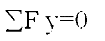
而每个小正方体所受到的压力,利用曲面积分的原理,对整个彩膜基板的弧面进行积分,得出每个小正方体所受到的压力:

其中,L为所述彩膜基板的长度,D为所述彩膜基板的曲率直径,r为所述彩膜基板的曲率半径,d为所述彩膜基板的厚度,
为所述彩膜基板的对应的圆心角,沿a方向小正方体单位面积上受到的压力Fa等于:

由于每个小正方体仅受到两个Fn的作用,因此沿a方向上单位面积上受到的压力的两倍,与每个小正方体所受到的压力相等,由公式3、4得出:

即公式5简化为:

相应地,所述彩膜基板受到总的压力为F0:

沿b方向上彩膜基板的面积Sb为:
Sb=πD*d 公式8
根据公式7、8得出沿b方向上小正方体单位面积上受到的压力为:

由于彩膜基板沿纸面向外方向所受的压力为零,因此

假设所述彩膜基板的弹性模量为E,弯曲过程中发生弹性形变,因而服从虎克定律,可以推断出彩膜基板内侧像素电极与彩膜色阻受到b方向压力(变形力)导致的弯曲偏移量k2为:

结合公式9,我们得出所述弯曲偏移量K2为:
K2=E*P*r/(8*d); 公式12
其中,K2为所述弯曲偏移量,K2的单位为米,E为所述彩膜基板的弹性模量,E的单位为兆帕、P为大气压强,P的单位为帕,通常P取标准大气压、r所述彩膜基板的曲率半径,r的单位为米、d为所述彩膜基板的厚度,d的单位为米。
即所述弯曲偏移量根据所述彩膜基板的厚度、所述彩膜基板的弹性模量以及所述彩膜基板的曲率半径获取,由于在将平面结构的液晶显示面板弯曲时,所述像素电极和彩膜色阻之间发生偏移,根据所述弯曲偏移量K2对黑色矩阵(BM)进行加宽处理,其中所述黑色矩阵的加宽值等于所述弯曲偏移量K2的值,通过加宽黑色矩阵的方法,从而使得所述像素电极和彩膜色阻之间重新一一对应,消除了曲面液晶显示面板出现的色偏问题,可以对整个彩膜基板的全部黑色矩阵都进行加宽。
优选地,所述曲面液晶显示面板包括左侧区域、中间区域、右侧区域,由于所述像素电极和彩膜色阻之间仅在左侧区域和右侧区域发生偏移,可根据所述弯曲偏移量仅对所述左侧区域和所述右侧区域的所述黑色矩阵进行加宽处理,其中所述黑色矩阵的加宽值等于所述弯曲偏移量的值。从而使得所述像素电极和彩膜色阻之间重新一一对应,消除了曲面液晶显示面板出现的色偏问题。同时由于所述黑色矩阵的加宽,使得所述黑色矩阵的宽度大于所述数据线的宽度(一般情况下黑色矩阵的宽度和数据线的宽度相等,黑色矩阵相对数据线设置),避免了当显示装置进一步弯曲时,彩膜基板与阵列基板的相对偏移量进一步增大,两个相邻的彩膜色阻移动到数据线附近,使得数据线附近的电场会引起液晶发生偏转,导致出现漏光的问题。
本发明的曲面液晶显示面板,通过对所述黑色矩阵进行加宽处理,从而消除了色偏、漏光等不良现象。
本发明还提供一种曲面液晶显示装置,该曲面液晶显示装置包括背光模块以及曲面液晶显示面板,该背光模块可包括光源以及导光板,光源用于提供出射光线,导光板用于将出射光线传导至曲面液晶显示面板上。曲面液晶显示面板包括曲面结构的彩膜基板、曲面结构的阵列基板以及液晶层,所述液晶层设置在所述彩膜基板和所述阵列基板之间。
所述彩膜基板,设置有彩膜色阻和黑色矩阵;
所述阵列基板,与所述彩膜基板相对设置,设置有像素电极和数据线,其中所述像素电极具有第一边和第二边,其中所述第一边的边长大于所述第二边的边长;其中所述曲面液晶显示面板的弯曲方向与所述第一边的延伸方向相同。
本发明的曲面液晶显示装置,可以采用上述任何一种曲面液晶显示面板,由于曲面液晶显示面板在上文已经详述,在此不再赘述。
本发明的曲面液晶显示装置,通过将曲面液晶显示面板的弯曲方向与像素电极的长边延伸方向保持一致,从而降低了色偏,同时避免了产生漏光现象,或者对所述黑色矩阵进行加宽处理,从而消除了色偏、漏光等不良现象。
综上所述,虽然本发明已以优选实施例揭露如上,但上述优选实施例并非用以限制本发明,本领域的普通技术人员,在不脱离本发明的精神和范围内,均可作各种更动与润饰,因此本发明的保护范围以权利要求界定的范围为准。
Claims (17)
- 一种曲面液晶显示面板,其包括:彩膜基板,设置有彩膜色阻和黑色矩阵;阵列基板,与所述彩膜基板相对设置,设置有像素电极和数据线,其中所述像素电极具有第一边和第二边,其中所述第一边的边长大于所述第二边的边长;其中所述曲面液晶显示面板的弯曲方向与所述第一边的延伸方向相同;以及液晶层,设置于所述彩膜基板和所述阵列基板之间;其中所述曲面液晶显示面板包括左侧区域、中间区域、右侧区域;根据弯曲偏移量对所述黑色矩阵进行加宽处理,且所述黑色矩阵的加宽值等于所述弯曲偏移量的值,以消除所述曲面液晶显示面板的色偏,所述弯曲偏移量为所述彩膜色阻与相应的像素电极之间的偏移量。
- 根据权利要求1所述的曲面液晶显示面板,其中根据所述彩膜基板的厚度、所述彩膜基板的弹性模量以及所述彩膜基板的曲率半径,获取所述弯曲偏移量。
- 根据权利要求2所述的曲面液晶显示面板,其中所述弯曲偏移量为:K=E*P*r/(8*d);其中,K为所述弯曲偏移量,E为所述彩膜基板的弹性模量、P为大气压强、r所述彩膜基板的曲率半径、d为所述彩膜基板的厚度。
- 根据权利要求1所述的曲面液晶显示面板,其中根据所述弯曲偏移量对所述左侧区域和所述右侧区域的所述黑色矩阵进行加宽处理。
- 根据权利要求1所述的曲面液晶显示面板,其中位于所述左侧区域的所述彩膜基板上的彩膜色阻相对所述阵列基板上相应的像素电极向左偏移,而位于所述右侧区域的所述彩膜基板上的彩膜色阻相对所述阵列基板上相应的像素电极向右偏移。
- 根据权利要求1所述的曲面液晶显示面板,其中所述彩膜色阻包括红色彩膜、绿色彩膜以及蓝色彩膜。
- 根据权利要求1所述的曲面液晶显示面板,其中所述像素电极和所述彩膜色阻相对设置。
- 一种曲面液晶显示面板,其包括:彩膜基板,设置有彩膜色阻和黑色矩阵;阵列基板,与所述彩膜基板相对设置,设置有像素电极和数据线,其中所述像素电极具有第一边和第二边,其中所述第一边的边长大于所述第二边的边长;其中所述曲面液晶显示面板的弯曲方向与所述第一边的延伸方向相同;以及液晶层,设置于所述彩膜基板和所述阵列基板之间。
- 根据权利要求8所述的曲面液晶显示面板,其中根据弯曲偏移量对所述黑色矩阵进行加宽处理,且所述黑色矩阵的加宽值等于所述弯曲偏移量的值,以消除所述曲面液晶显示面板的色偏,其中所述弯曲偏移量为所述彩膜色阻与相应的像素电极之间的偏移量。
- 根据权利要求9所述的曲面液晶显示面板,其中根据所述彩膜基板的厚度、所述彩膜基板的弹性模量以及所述彩膜基板的曲率半径,获取所述弯曲偏移量。
- 根据权利要求10所述的曲面液晶显示面板,其中所述弯曲偏移量为:K=E*P*r/(8*d);其中,K为所述弯曲偏移量,E为所述彩膜基板的弹性模量、P为大气压强、r所述彩膜基板的曲率半径、d为所述彩膜基板的厚度。
- 根据权利要求9所述的曲面液晶显示面板,其中所述曲面液晶显示面板包括左侧区域、中间区域、右侧区域,根据所述弯曲偏移量对所述左侧区域和所述右侧区域的所述黑色矩阵进行加宽处理。
- 一种曲面液晶显示装置,其包括背光模块;及曲面液晶显示面板,所述曲面液晶显示面板包括:彩膜基板,设置有彩膜色阻和黑色矩阵;阵列基板,与所述彩膜基板相对设置,设置有像素电极和数据线,其中所述像素电极具有第一边和第二边,其中所述第一边的边长大于所述第二边的边长;其中所述曲面液晶显示面板的弯曲方向与所述第一边的延伸方向相同;以及液晶层,设置于所述彩膜基板和所述阵列基板之间。
- 根据权利要求13所述的曲面液晶显示装置,其中根据弯曲偏移量对所述黑色矩阵进行加宽处理,且所述黑色矩阵的加宽值等于所述弯曲偏移量的值,以消除所述曲面液晶显示面板的色偏,其中所述弯曲偏移量为所述彩膜色阻与相应的像素电极之间的偏移量。
- 根据权利要求14所述的曲面液晶显示装置,其中根据所述彩膜基板的厚度、所述彩膜基板的弹性模量以及所述彩膜基板的曲率半径,获取所述弯曲偏移量。
- 根据权利要求15所述的曲面液晶显示装置,其中所述弯曲偏移量为:K=E*P*r/(8*d);其中,K为所述弯曲偏移量,E为所述彩膜基板的弹性模量、P为大气压强、r所述彩膜基板的曲率半径、d为所述彩膜基板的厚度。
- 根据权利要求14所述的曲面液晶显示装置,其中所述曲面液晶显示面板包括左侧区域、中间区域、右侧区域,根据所述弯曲偏移量对所述左侧区域和所述右侧区域的所述黑色矩阵进行加宽处理。
Priority Applications (1)
| Application Number | Priority Date | Filing Date | Title |
|---|---|---|---|
| US14/416,588 US9568762B2 (en) | 2014-11-13 | 2014-12-16 | Curved liquid crystal display panel and curved liquid crystal display device |
Applications Claiming Priority (2)
| Application Number | Priority Date | Filing Date | Title |
|---|---|---|---|
| CN201410639864.8A CN104375339B (zh) | 2014-11-13 | 2014-11-13 | 曲面液晶显示面板及曲面液晶显示装置 |
| CN201410639864.8 | 2014-11-13 |
Publications (1)
| Publication Number | Publication Date |
|---|---|
| WO2016074310A1 true WO2016074310A1 (zh) | 2016-05-19 |
Family
ID=52554358
Family Applications (1)
| Application Number | Title | Priority Date | Filing Date |
|---|---|---|---|
| PCT/CN2014/093909 Ceased WO2016074310A1 (zh) | 2014-11-13 | 2014-12-16 | 曲面液晶显示面板及曲面液晶显示装置 |
Country Status (3)
| Country | Link |
|---|---|
| US (1) | US9568762B2 (zh) |
| CN (1) | CN104375339B (zh) |
| WO (1) | WO2016074310A1 (zh) |
Families Citing this family (16)
| Publication number | Priority date | Publication date | Assignee | Title |
|---|---|---|---|---|
| JP6019997B2 (ja) | 2012-09-26 | 2016-11-02 | ソニー株式会社 | 表示装置および電子機器 |
| KR102257106B1 (ko) * | 2015-01-06 | 2021-05-27 | 삼성디스플레이 주식회사 | 액정 표시 장치 |
| CN105093727B (zh) * | 2015-09-24 | 2018-11-06 | 京东方科技集团股份有限公司 | 一种阵列基板、曲面显示面板、曲面显示装置 |
| CN105290749A (zh) * | 2015-11-04 | 2016-02-03 | 武汉华星光电技术有限公司 | 组装贴合设备 |
| CN105259716B (zh) * | 2015-11-24 | 2018-08-03 | 京东方科技集团股份有限公司 | 一种阵列基板、曲面显示面板及曲面显示装置 |
| CN105445993B (zh) * | 2015-12-08 | 2018-09-14 | 南京中电熊猫液晶显示科技有限公司 | 一种曲面液晶面板 |
| CN105866998A (zh) * | 2016-06-02 | 2016-08-17 | 京东方科技集团股份有限公司 | 显示装置 |
| US10254579B2 (en) * | 2016-07-29 | 2019-04-09 | Lg Display Co., Ltd. | Curved display device |
| TWI589972B (zh) * | 2016-12-28 | 2017-07-01 | 友達光電股份有限公司 | 主動元件陣列基板及應用其之液晶面板 |
| CN107067984A (zh) * | 2017-06-09 | 2017-08-18 | 京东方科技集团股份有限公司 | 曲面显示面板的制作方法、曲面显示面板及曲面显示装置 |
| RU2659956C1 (ru) * | 2017-08-01 | 2018-07-04 | Андрей Иванович Шуда | Мобильная система информирования |
| CN108132560B (zh) * | 2018-01-03 | 2020-05-22 | 厦门天马微电子有限公司 | 显示面板及显示装置 |
| CN108399863B (zh) * | 2018-03-22 | 2020-08-21 | 京东方科技集团股份有限公司 | 一种柔性显示装置及其驱动方法 |
| CN108873444B (zh) * | 2018-07-17 | 2021-11-09 | Tcl华星光电技术有限公司 | 柔性导光板及柔性显示器 |
| CN111048563B (zh) * | 2019-12-17 | 2022-05-10 | 武汉天马微电子有限公司 | 柔性显示面板及柔性显示装置 |
| CN111446277B (zh) * | 2020-04-13 | 2023-06-23 | 京东方科技集团股份有限公司 | 显示基板及显示装置 |
Citations (5)
| Publication number | Priority date | Publication date | Assignee | Title |
|---|---|---|---|---|
| JP2007333818A (ja) * | 2006-06-12 | 2007-12-27 | Sharp Corp | 表示パネル |
| CN101201486A (zh) * | 2006-12-11 | 2008-06-18 | 龙腾光电(控股)有限公司 | 弯曲液晶面板及液晶显示装置 |
| JP2010008875A (ja) * | 2008-06-30 | 2010-01-14 | Mitsubishi Electric Corp | 液晶表示装置及び製造方法 |
| CN103605228A (zh) * | 2013-11-27 | 2014-02-26 | 青岛海信电器股份有限公司 | 显示设备和液晶电视机 |
| CN104111567A (zh) * | 2014-08-08 | 2014-10-22 | 深圳市华星光电技术有限公司 | 曲面液晶面板 |
Family Cites Families (1)
| Publication number | Priority date | Publication date | Assignee | Title |
|---|---|---|---|---|
| KR20150047399A (ko) * | 2013-10-24 | 2015-05-04 | 삼성디스플레이 주식회사 | 액정표시패널 |
-
2014
- 2014-11-13 CN CN201410639864.8A patent/CN104375339B/zh not_active Expired - Fee Related
- 2014-12-16 US US14/416,588 patent/US9568762B2/en active Active
- 2014-12-16 WO PCT/CN2014/093909 patent/WO2016074310A1/zh not_active Ceased
Patent Citations (5)
| Publication number | Priority date | Publication date | Assignee | Title |
|---|---|---|---|---|
| JP2007333818A (ja) * | 2006-06-12 | 2007-12-27 | Sharp Corp | 表示パネル |
| CN101201486A (zh) * | 2006-12-11 | 2008-06-18 | 龙腾光电(控股)有限公司 | 弯曲液晶面板及液晶显示装置 |
| JP2010008875A (ja) * | 2008-06-30 | 2010-01-14 | Mitsubishi Electric Corp | 液晶表示装置及び製造方法 |
| CN103605228A (zh) * | 2013-11-27 | 2014-02-26 | 青岛海信电器股份有限公司 | 显示设备和液晶电视机 |
| CN104111567A (zh) * | 2014-08-08 | 2014-10-22 | 深圳市华星光电技术有限公司 | 曲面液晶面板 |
Also Published As
| Publication number | Publication date |
|---|---|
| US20160139458A1 (en) | 2016-05-19 |
| CN104375339B (zh) | 2017-07-18 |
| US9568762B2 (en) | 2017-02-14 |
| CN104375339A (zh) | 2015-02-25 |
Similar Documents
| Publication | Publication Date | Title |
|---|---|---|
| WO2016074310A1 (zh) | 曲面液晶显示面板及曲面液晶显示装置 | |
| WO2016082235A1 (zh) | 曲面显示面板及曲面显示装置 | |
| WO2018080055A1 (en) | Display apparatus | |
| WO2014121527A1 (zh) | 一种改善液晶屏的视角肤色色偏的方法及系统 | |
| WO2016074263A1 (zh) | 曲面液晶显示面板及曲面液晶显示装置 | |
| WO2019059528A1 (en) | DISPLAY DEVICE | |
| WO2013166736A1 (zh) | 液晶显示面板和液晶显示器 | |
| WO2020073438A1 (zh) | 显示面板和显示装置 | |
| WO2013163824A1 (zh) | 液晶显示面板、液晶显示器及3d影像系统 | |
| WO2016095251A1 (zh) | 一种液晶显示面板的制作方法 | |
| WO2021213430A1 (zh) | 显示基板及其制造方法、显示装置 | |
| WO2017152446A1 (zh) | 一种液晶显示面板及装置 | |
| WO2021104404A1 (zh) | 显示模组及电子设备 | |
| WO2014047987A1 (zh) | 一种液晶面板及其制作方法 | |
| WO2017181463A1 (zh) | 阵列基板及其制造方法、液晶显示器 | |
| WO2016155030A1 (zh) | 显示面板及显示装置 | |
| US20170229417A1 (en) | Mounting substrate manufacturing apparatus and method of manufacturing mounting substrate | |
| WO2014110839A1 (zh) | 液晶显示器 | |
| WO2013143094A1 (zh) | 背光模组及液晶显示器 | |
| CN101135806A (zh) | 偏振板、液晶装置以及电子设备 | |
| CN101341437A (zh) | 液晶显示器件及具有该液晶显示器件的移动通信终端 | |
| WO2016041216A1 (zh) | 一种液晶显示面板 | |
| WO2011013889A1 (en) | Backlight unit and display apparatus including the same | |
| WO2016175641A1 (ko) | 액정 디스플레이 장치 및 이의 제조방법 | |
| WO2019218819A1 (zh) | 光源装置、背光模组及液晶显示装置 |
Legal Events
| Date | Code | Title | Description |
|---|---|---|---|
| WWE | Wipo information: entry into national phase |
Ref document number: 14416588 Country of ref document: US |
|
| 121 | Ep: the epo has been informed by wipo that ep was designated in this application |
Ref document number: 14905991 Country of ref document: EP Kind code of ref document: A1 |
|
| NENP | Non-entry into the national phase |
Ref country code: DE |
|
| 122 | Ep: pct application non-entry in european phase |
Ref document number: 14905991 Country of ref document: EP Kind code of ref document: A1 |