WO2016060401A1 - 다중모드 공진기 - Google Patents
다중모드 공진기 Download PDFInfo
- Publication number
- WO2016060401A1 WO2016060401A1 PCT/KR2015/010593 KR2015010593W WO2016060401A1 WO 2016060401 A1 WO2016060401 A1 WO 2016060401A1 KR 2015010593 W KR2015010593 W KR 2015010593W WO 2016060401 A1 WO2016060401 A1 WO 2016060401A1
- Authority
- WO
- WIPO (PCT)
- Prior art keywords
- resonant
- ribs
- resonator
- housing
- resonance
- Prior art date
Links
Images


Classifications
-
- H—ELECTRICITY
- H01—ELECTRIC ELEMENTS
- H01P—WAVEGUIDES; RESONATORS, LINES, OR OTHER DEVICES OF THE WAVEGUIDE TYPE
- H01P7/00—Resonators of the waveguide type
- H01P7/10—Dielectric resonators
- H01P7/105—Multimode resonators
-
- H—ELECTRICITY
- H01—ELECTRIC ELEMENTS
- H01P—WAVEGUIDES; RESONATORS, LINES, OR OTHER DEVICES OF THE WAVEGUIDE TYPE
- H01P7/00—Resonators of the waveguide type
- H01P7/06—Cavity resonators
-
- H—ELECTRICITY
- H01—ELECTRIC ELEMENTS
- H01P—WAVEGUIDES; RESONATORS, LINES, OR OTHER DEVICES OF THE WAVEGUIDE TYPE
- H01P1/00—Auxiliary devices
- H01P1/20—Frequency-selective devices, e.g. filters
- H01P1/201—Filters for transverse electromagnetic waves
- H01P1/205—Comb or interdigital filters; Cascaded coaxial cavities
- H01P1/2053—Comb or interdigital filters; Cascaded coaxial cavities the coaxial cavity resonators being disposed parall to each other
-
- H—ELECTRICITY
- H01—ELECTRIC ELEMENTS
- H01P—WAVEGUIDES; RESONATORS, LINES, OR OTHER DEVICES OF THE WAVEGUIDE TYPE
- H01P1/00—Auxiliary devices
- H01P1/20—Frequency-selective devices, e.g. filters
- H01P1/207—Hollow waveguide filters
- H01P1/208—Cascaded cavities; Cascaded resonators inside a hollow waveguide structure
- H01P1/2082—Cascaded cavities; Cascaded resonators inside a hollow waveguide structure with multimode resonators
-
- H—ELECTRICITY
- H01—ELECTRIC ELEMENTS
- H01P—WAVEGUIDES; RESONATORS, LINES, OR OTHER DEVICES OF THE WAVEGUIDE TYPE
- H01P7/00—Resonators of the waveguide type
- H01P7/04—Coaxial resonators
-
- H—ELECTRICITY
- H01—ELECTRIC ELEMENTS
- H01P—WAVEGUIDES; RESONATORS, LINES, OR OTHER DEVICES OF THE WAVEGUIDE TYPE
- H01P1/00—Auxiliary devices
- H01P1/20—Frequency-selective devices, e.g. filters
- H01P1/207—Hollow waveguide filters
- H01P1/208—Cascaded cavities; Cascaded resonators inside a hollow waveguide structure
- H01P1/2084—Cascaded cavities; Cascaded resonators inside a hollow waveguide structure with dielectric resonators
- H01P1/2086—Cascaded cavities; Cascaded resonators inside a hollow waveguide structure with dielectric resonators multimode
Definitions
- the present invention relates to a resonator for implementing a radio frequency filter, and more particularly to a multi-mode resonator for outputting the resonant frequency of a plurality of resonant modes.
- Radio frequency devices such as radio frequency filters, typically consist of a connection structure of a plurality of resonators.
- a resonator is an equivalent electronic circuit that is a circuit element that resonates at a specific frequency by a combination of an inductor L and a capacitor C.
- Each resonator has a dielectric inside a cavity such as a metallic cylinder or a cube surrounded by a conductor. It has a structure in which a resonant element (DR) or a metal resonant element is provided. Accordingly, each resonator has a structure in which only the electromagnetic field of the natural frequency corresponding to the processing frequency band is present in the cavity, thereby enabling ultra high frequency resonance.
- one cavity is formed for each cavity, and a plurality of resonance stages are sequentially connected.
- the bandpass filter 10 includes a housing 110 having six cavities, for example, partitioned at predetermined intervals inside a metal of a hexahedron. Each cavity has a structure in which eight dielectric or metal resonating elements 122 having a high Q value are fixed by using a supporting support.
- the input / output connectors 111 and 113 mounted on one side of the housing 110 and a cover 160 that shields the open surface of the housing 110 are provided.
- each cavity of the housing 110 is partitioned by a partition wall 130 in which windows 131 to 135 of a predetermined size are formed in order to adjust the coupling amount of each resonance period, and an inner surface of the housing 110.
- Silver has a silver-plated structure to stabilize electrical performance and maximize conductivity.
- a coupling screw 175 is further provided to penetrate the cover 160 or the housing 110 into the windows 131-135, whereby the amount of coupling can be finely adjusted.
- each resonator element 122 is supported by a support support provided upright on the bottom surface, the tuning screw 170 for adjusting the frequency penetrates the cover 160 on the upper surface of each resonator element 122. It can be installed to be inserted into the cavity, by adjusting it to enable a fine adjustment for the resonance frequency.
- One side of the housing 110 is provided with input / output connectors 111 and 113, respectively, which are connected to input / output feed lines (not shown), respectively.
- the input side feed line transmits a signal coming from the input connector to the first stage resonating element.
- the output side feed line serves to transmit a signal from the resonant element of the last stage to the output connector.
- Korean Patent Publication No. 10-2004-100084 name: “radio frequency filter”, published by the applicant of the present application), published date: December 2004 On the day 02, the inventors: Park Jong-kyu, Park Sang-sik, Seung-taek Jung) are mentioned as an example.
- a filter having a multi-mode resonator structure is one of the devices occupying the most space among communication equipment, and active research is continuously conducted to reduce the size and weight of the filter.
- each base station is evolving into a small (or ultra-small) cell, and accordingly, miniaturization and weight reduction of the filter are required more importantly. have.
- an object of the present invention is to provide a multi-mode resonator capable of connecting a plurality of same-mode resonant frequencies to each other well.
- Another object of the present invention is to provide a miniaturized multimode resonator.
- Another object of the present invention to provide a multi-mode resonator that can reduce the manufacturing cost.
- the present invention provides a multimode resonator;
- a housing provided with a cavity corresponding to substantially one accommodation space;
- a plurality of resonant ribs are arranged in the cavity at predetermined intervals, the lower end is fixed to the bottom surface of the housing and the upper end is opposite to each other, generating a resonance signal by the complex coupling between the plurality of resonant ribs It is characterized by including.
- the plurality of resonant ribs are bar-shaped bent in the shape of an arch as a whole, the cross-sectional shape may be substantially circular.
- At least some of the upper ends of the plurality of resonant ribs may have a cut shape.
- the lower end portions of the plurality of resonant ribs may be manufactured in a state of being integrally connected as a whole by one connecting auxiliary support having a ring shape.
- the lower end portions of the plurality of resonant ribs may be manufactured to be integrally connected to the housing as a whole extending in the bottom surface of the housing.
- the multi-mode resonator according to embodiments of the present invention has an advantage of providing a multi-mode resonant frequency to one resonator. In addition, this has the advantage that can be reduced in size, weight and manufacturing cost of the filter. In particular, the multi-mode resonator according to the embodiments of the present invention hardly occurs an assembly tolerance between components, so that the frequency tuning operation of the filter can be made very simple and efficient.
- FIG. 1 is an exploded perspective view of an example of a conventional six-pole type bandpass filter
- FIGS. 2A to 2C are structural diagrams of a multimode resonator corresponding to a bandpass filter according to a first embodiment of the present invention.
- 3A to 3E are diagrams illustrating respective multimode resonance characteristics of a multimode resonator corresponding to a bandpass filter according to a first embodiment of the present invention.
- FIG. 4 is a graph showing frequency filtering characteristics of a multimode resonator corresponding to a bandpass filter according to a first embodiment of the present invention
- 5A to 5C are structural diagrams of a multimode resonator corresponding to a bandpass filter according to a second embodiment of the present invention.
- FIGS. 6A to 6D are structural diagrams of a multimode resonator corresponding to a bandpass filter according to a third embodiment of the present invention.
- FIG. 7 is a diagram illustrating respective multimode resonance characteristics of one modified structure of a multimode resonator corresponding to a bandpass filter according to a third embodiment of the present invention.
- FIG. 8 is a diagram illustrating respective multimode resonance characteristics of another modified structure of a multimode resonator corresponding to a bandpass filter according to a third embodiment of the present invention.
- FIG. 9 is a graph illustrating frequency filtering characteristics of a multimode resonator corresponding to a bandpass filter according to a third embodiment of the present invention.
- 10A to 10D illustrate another modified structure of the multimode resonator corresponding to the bandpass filter according to the third embodiment of the present invention.
- FIG. 11 is a diagram illustrating respective multimode resonance characteristics of the multimode resonators of FIGS. 10A to 10D.
- FIG. 12 is a graph showing frequency filtering characteristics according to the multimode resonator of FIGS. 10A to 10D.
- FIGS. 13A to 13D are structural diagrams of a multimode resonator corresponding to a bandpass filter according to a fourth embodiment of the present invention.
- FIGS. 14A to 14D are diagrams illustrating one modified structure of a multimode resonator corresponding to a bandpass filter according to a fourth embodiment of the present invention.
- 15A to 15D are structural diagrams of a multimode resonator corresponding to a bandpass filter according to a fifth embodiment of the present invention.
- 16A to 16C are structural diagrams of a multimode resonator corresponding to a bandpass filter according to a sixth embodiment of the present invention.
- FIG. 17 is a diagram illustrating respective multimode resonance characteristics of a multimode resonator according to a sixth exemplary embodiment of the present invention.
- 18A to 18C are structural diagrams of a multimode resonator corresponding to a bandpass filter according to a seventh embodiment of the present invention.
- the present invention proposes a multiple resonance mode filter that provides a plurality of resonance modes. Conventionally, for example, in order to provide four resonance modes, it is common to have four cavities and one resonant element in each cavity. However, the multiple resonance mode filter according to the present invention can provide four resonance modes, five resonance modes, and the like in one cavity.
- FIGS. 2A to 2C are structural diagrams of a multi-mode resonator corresponding to a bandpass filter according to a first embodiment of the present invention.
- FIG. 2A a partial (resonant rod portion) transmission perspective structure
- FIG. 2B is a planar structure
- FIG. One side structure is shown.
- the resonator shown in FIGS. 2A to 2C has a cavity 200 formed by a metal housing (under cover), similar to a conventional filter structure, which is shown in FIGS. 2A to 2C for convenience of description.
- the illustration of the input and output connectors and the like formed on the outside of the housing is omitted.
- the multi-mode resonator according to the first embodiment of the present invention has a cavity similar to the shape of a square box or a square box in which one accommodation space is formed substantially inside the housing (not shown). 200).
- the cavity 200 may have various structures such as a polygonal pillar shape or a cylindrical shape in addition to the box shape as described above.
- the cavity 200 includes a plurality of resonant arms disposed at predetermined intervals.
- the plurality of resonance arms may be made of a metallic material, and may be installed at equal intervals.
- the plurality of resonant arms may be arranged in pairs so that one end thereof faces each other, and the pairs may be arranged to cross each other.
- resonant arms adjacent to each other have an arrangement structure in which they are orthogonal to each other, and are separately installed separately.
- Four resonant arms 211, 212, 213, 214 are provided.
- the four resonant arms 211-214 that is, the first to fourth resonant arms 211-214 may be disposed to have a '+' shape as a whole (planarly), that is, the four resonant arms 211-214.
- the center position of the entire arrangement structure of 214 may correspond to the center position of the cavity 200.
- the four resonant arms 211-214 may each have a rod-shaped rectangular parallelepiped formed in the longitudinal direction.
- the four resonant arms 211-214 each extend from (or be fixed to, the bottom surface) of the bottom surface (inner bottom surface of the housing) of the cavity 200, for example, made of a metallic material. It can be fixedly installed by the first to fourth resonant legs (221, 222, 223, 224) of the cylindrical form.
- the first to fourth resonant legs 221 to 224 may be manufactured integrally with the bottom surface through a die casting process, for example, when the bottom surface of the housing forming the cavity 200 is formed. Each may be manufactured separately and fixedly attached to the bottom surface of the housing by welding, soldering, screwing, or the like. Similarly, the first to fourth resonant arms 211 to 214 may be integrally manufactured at the time of forming the first to fourth resonant legs 221 to 224, respectively. It may be fixedly attached to the first to fourth resonant legs (221-224).
- the resonating element in the conventional filter structure is located at the center position of the entire arrangement structure of the four resonant arms 211-214, that is, the center position of the cavity 200.
- a resonator rod 215 of similar construction is further installed.
- the four resonant arms 211-214 and the resonant rods 215 are physically spaced apart from each other, but have an appropriate separation distance from each other so that the signals therebetween can be combined with each other. Of course, the amount of signal coupling between each other is adjusted by adjusting the separation distance.
- the overall structure of the four resonant arms 211-214 is a structure in which the four resonant arms 211-214 are complexly coupled to each other, unlike a structure in which a conventional resonator is sequentially coupled.
- the arrangement structure of the four resonant arms (211-214) and the resonator rods 215 is orthogonal to each other around the center position of the cavity 200 structure, for example, x
- the first resonance arm 211 and the third resonance arm 213 are disposed on the x axis
- the second resonance arm 212 and the fourth resonance Arm 214 is disposed on the y axis
- resonant rod 215 may be considered to be disposed on the z axis.
- the input connector (not shown) and the output connector (not shown) may be formed at one pole of the x-axis and the y-axis, respectively, and the input probe 231 and one of the y-axis to be connected to the input connector formed at the one pole of the x-axis.
- An output probe 223 is provided to be connected to an output connector formed at a pole, and the input probe 231 and the output probe 232 may be any one of a pair of resonant arms and input / output signals of the plurality of resonant arms 211-214. It is configured to send and receive. In the example of FIG.
- the input probe 231 and the output probe 232 are directly and indirectly connected to the third resonance leg 223 and the second resonance leg 222, respectively, and transmit an input / output signal. It is configured to exchange input and output signals with the third resonant arm 213 and the second resonant arm 212.
- FIGS. 3A to 3E Multimode resonance characteristics of the resonator having the above structure are shown in FIGS. 3A to 3E.
- FIG. 3A shows the magnetic field (or electric field) of the first resonant mode formed by the entire combination (coupling) of the resonant structure
- FIG. 3B is illustrated by, for example, the second and fourth resonant arms 212, 214.
- FIG. 3C is, for example, in the x-axis direction by the first and third resonant arms 211 and 213.
- 3D shows the magnetic field (or electric field) of the fourth resonance mode formed by the entire combination of the first to fourth resonance arms 211-214.
- 3E illustrates a magnetic field (or electric field) of the fifth resonant mode in which dominant resonance is formed in the z-axis direction by, for example, the resonance rod 215.
- E-field characteristics are shown in each (a)
- H-field characteristics are shown in each (b).
- FIG. 4 is an exemplary graph illustrating frequency filtering characteristics according to the resonators of FIGS. 2A to 2C. Referring to FIG. 4, it can be seen that frequency filtering characteristics appear according to five multi-mode characteristics, as shown in FIGS. 3A to 3E.
- the multi-mode resonator according to the first embodiment of the present invention can implement five resonant modes in one cavity 200.
- the multi-mode resonator of the structure according to the present invention has a general structure of the same size. Compared with the TEM mode resonator of, when the Q (Quality factor) value has about 30 ⁇ 40% improvement in the same size or when the same Q value is satisfied, the physical size of the resonator is compared with the general structure. It can be reduced to about 30-40%.
- FIGS. 5A to 5C are structural diagrams of a multi-mode resonator corresponding to a bandpass filter according to a second embodiment of the present invention.
- FIG. 5A shows a partially transmissive perspective structure, a planar structure in FIG. 5B, and a side structure in FIG. 5C. have.
- the housing (not shown) forming the cavity 300 is omitted for convenience of description as in FIGS. 2A to 2C.
- Resonator according to the second embodiment of the present invention shown in Figure 5 is somewhat similar to the structure of the first embodiment shown in Figs. 2a to 2c, the cavity 300 is substantially provided in one receiving space A housing (not shown); A plurality of resonant arms (311, 312, 313) disposed at predetermined intervals in the cavity (300) and generating a resonance signal by a complex coupling with each other; A plurality of resonant legs (321, 322, 323) for supporting the plurality of resonant arms (311-313), respectively.
- the cavity 300 is formed in a cylindrical shape as a whole.
- the plurality of resonant arms 311, 312, and 313 are first to third resonant arms 311-313, and a total of three are arranged at equal intervals from each other. That is, as in the second embodiment of FIGS. 3A to 3C, the three resonant arms 311-313 in the form of rods in the cavity 200 have one end facing the center of the cavity 300, and so on. Are placed at intervals.
- the plurality of resonant legs 321-323 are also the first to third resonant legs 321-323, and the three resonant legs 321-323 are respectively the first to third resonant arms 311-313. ) Is installed to support.
- the input probe 331 and the output probe 332 may be connected to the first resonance leg 321 and the third resonance leg 323, respectively.
- the resonator rod is removed from the structure of the first embodiment (that is, without the resonator rod).
- the structure of the resonator according to the second embodiment shown in FIGS. 5A to 5C is suitable for implementing four or three resonant modes as compared with the structure of the first embodiment, and has sufficient satisfactory multimode characteristics. You can get it.
- the corner portions of the three resonant arms 311-313 in the form of respective rectangular bars are cut through processing such as chamfering.
- the characteristics such as coupling strength are adjusted by such a structural change.
- 5A to 5C show an example in which two portions of the edge portions of the three resonant arms 311 to 313 facing each other are cut off.
- the coupling strength or the generation of notches may be adjusted through changes in the structure in which the edges of the resonance arm are cut such as chamfers.
- the first to third resonant legs 321 to 323 are provided to be spaced apart from each other as much as possible. That is, the first to third resonant legs 321 to 323 are coupled to the outer portions of the first to third resonant arms 311 to 313 based on the central position of the cavity 300 to support the corresponding resonant arms. Is installed.
- a diaphragm or a tuning screw may be additionally installed at an appropriate position, including between the input and output sides of the signal. This causes perturbation between the respective resonant arms, thereby adjusting the position of the transmission zero and the formation of notches.
- a multi-mode resonator according to the first and second embodiments of the present invention may be constructed, and in the structure of the first and second embodiments, There may be variations, modifications and applications.
- the resonant arms 211-214 or 311-314 may not be equal in length to each other.
- the length of one pair may be set differently from the length of the other pair.
- there may be some differences in the diameter, shape, and the like. This configuration is intended to change the position of the transmission zero point, and to change the strength and direction of the field coupled between the resonant arms, thereby adjusting the notch point.
- the resonant legs 221-224 or 321-323 may be designed to be different from each other in diameter, length, and the like.
- the capacitance component generated between the resonance arm and the cavity may be adjusted by narrowing or widening the distance between the cavity and the cavity 200 or 300 supported by the resonance leg.
- a metallic coupling structure in the form of a cylinder or a disk may be further provided.
- This coupling structure allows for better coupling between the coupling resonant arms as compared to the absence of the corresponding coupling structure, thereby widening the overall bandwidth of the filter.
- This coupling structure may be installed to be fixed and supported in the cavity by the support member (not shown) made of materials such as Al 2 O 3 and Teflon, or on the inner surface of the housing or cover, or adjacent resonance arms.
- a tuning screw (not shown) may be installed at a central position of the entire structure of the resonant arms 211-214 or 311-314 in such a manner as to penetrate a cover or the like at the top of the housing. You may. Through such a tuning screw, the signal coupling between the resonant arms, and thus the coupling adjustment between the resonant modes and the resonant frequency tuning may be performed.
- the resonator according to the first embodiment or the resonator according to the second embodiment may have a structure formed of a double.
- the resonators according to the first and second embodiments may be coupled to each other.
- a first resonator and a second resonator according to the first (or second) embodiment are formed, and an output side of the first resonator and an input side of the second resonator may be connected to each other by a coupling window.
- the coupling window may additionally be provided with a conductive coupling structure of a suitable structure which is formed to elongate at the bottom surface of the cavity (ie the inner bottom surface of the housing) so as to make the coupling better.
- the resonance arms (211-214 or 311-314) It can be seen that precise spacing of the liver is a very important factor in its characteristics. However, in the first and second embodiments, since the resonant arms 211-214 or 311-314 are fixed to the resonant legs 221-224 or 321-323 by screwing, etc., assembly is performed. The tolerance causes the spacing between the resonant arms 211-214 or 311-314 to be slightly different compared to the designed dimensions.
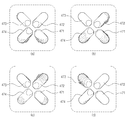
- FIG. 6A to 6D are structural diagrams of a multimode resonator corresponding to a bandpass filter according to a third embodiment of the present invention.
- FIG. 6A is a perspective structure
- FIG. 6B is a planar structure
- FIG. 6C is a side structure
- FIG. The back structure is shown.
- the resonator according to the third embodiment of the present invention shown in Figs. 6A to 6D has a cavity 400 in which a space is formed by a metal housing (bottom cover), similar to a conventional filter structure.
- illustrations of the input / output connector formed on the outside of the housing as well as the structure of the metal housing are omitted for convenience of description.
- the multi-mode resonator according to the third embodiment of the present invention similar to the first embodiment shown in FIGS. 2A to 2C, has a cavity 400 similar in shape to a square box.
- the structure of the cavity 400 may have various structures such as a polygonal pillar shape or a cylindrical shape in addition to the square box shape as described above.
- the cavity 400 is located within the cavity 400.
- the lower end is fixed to the bottom surface of the cavity 400 (that is, the inner bottom surface of the housing) and the upper end is installed facing each other, generating a resonance signal by the complex coupling between each other
- the four resonant ribs 441-444 that is, the first to fourth resonant ribs 441-444 may be disposed to have an 'x' shape as a whole (planarly).
- the arch shape of the resonant ribs 441-444 can be designed along the trajectory of a portion of an arc, for example.
- the input probe 431 and the output probe 432 may be connected to the first resonance rib 441 and the fourth resonance rib 444, respectively.
- the position at which the input probe 431 and the output probe 432 are installed may also affect the magnetic field (resonance characteristic) of the multimode resonator.
- the input probe 431 and the output probe 432 may be connected to any one of the first to fourth resonant ribs 441-444 according to the use conditions of the multimode resonator.
- the input probe 431 may be connected to the third resonant rib 443, and the output probe 432 may be connected to the first resonant rib 441.
- the resonant ribs 441-444 respectively replace the plurality of resonant arms and the resonant legs in the first and second embodiments, and the bottom surface of the cavity 400 in the resonant ribs 441-444. (I.e., an inner bottom surface of the housing) serves as a resonant leg in the first and second embodiments, and a portion facing each other serves as a resonant arm in the first and second embodiments.
- the resonant ribs 441-444 have a structure in which a plurality of resonant arms and resonant legs are integrally formed (to reduce the assembly tolerance) in the first and second embodiments, respectively.
- the resonant ribs 441-444 do not have a shape in which a portion corresponding to the resonance arm and a portion corresponding to the resonance leg are not distinguished from each other, as in the first and second embodiments. It has a rod-shaped bent in the shape of an arch.
- the resonant ribs 441-444 have a substantially circular cross-sectional shape.
- the filter has satisfactory filtering characteristics even through the resonant ribs in the shape as described above.
- Such a shape eliminates angled portions, so that signal (current) flowability can be improved to improve filtering characteristics.
- such a shape does not require a draft angle shape when manufacturing the resonant ribs by the die casting process, and it can be seen that the optimal structure does not require a R (Round) treatment on the edge of the product.
- the frequency of each resonant mode is shifted and the appropriate frequency is changed by changing the shape, length, and width of the first to fourth resonant ribs 441-444. It is possible to set and adjust the resonance mode.
- the resonant ribs 441-444 have a shape in which a part of the side surface of the edge portion of the (top) end facing each other is cut through processing such as chamfering, By such a structural change, coupling strength or notch generation can be controlled.
- FIGS. 6A to 6D some of the upper portions of the end portions of the resonant ribs 441-444 facing each other, that is, the upper end portion, are further cut.
- the capacitance component generated between the resonance rib and the cavity can be adjusted.
- the upper cut portions of the second and third resonant ribs 442 and 443 are larger than the upper cut portions of the first and fourth resonant ribs 441 and 444.
- the cut state is shown by way of example.
- FIG. 7 is a diagram illustrating an example of each multimode resonance characteristic of one modified structure of a multimode resonator corresponding to a bandpass filter according to a third embodiment of the present invention.
- FIGS. 6A to 6D Multimode resonance characteristics are shown when the cutting portions of the resonant ribs 441-444 shown in FIG. 4 are all the same (symmetrical to each other) structure.
- 7 (a) and 7 (b) show magnetic fields of the first and second resonance modes formed by, for example, the entire combination of the first to fourth resonant ribs 441'-444 '.
- the first resonant rib 441 ′ and the third resonant rib 443 ′ are paired to generate a magnetic field having the same polarity
- the second resonant rib 442 and the fourth resonant rib 444 Represents a case where a magnetic field having a polarity different from that of the first and third resonance ribs 441 ′ and 443 ′ is generated in pairs. They are combined (coupled) as a whole to form one resonant mode, in which case they may have a relatively minimal Q value of the four modes.
- FIG. 7B all of the first to fourth resonant ribs 441 ′ -444 ′ generate magnetic fields having the same polarity, and these are combined to form one resonance mode in which four modes are used. The largest Q value may appear.
- FIG. 7C and 7D illustrate, for example, a pair of first and third resonant ribs 441'-443 'and a pair of second and fourth resonant ribs 442'-444', respectively.
- the magnetic field of the third and fourth resonance modes formed by the combination is shown.
- FIG. 7D when the second and fourth resonant ribs 442 'and 444' each generate magnetic fields having different polarities, the resonance modes formed by these combinations are shown. In this case, a Q value similar to that of FIG. 7C may appear.
- various magnetic field distributions between symmetric resonant ribs can be made by changing physical set values and changing the strength and direction of the magnetic field.
- FIG. 8 is a diagram illustrating respective multimode resonance characteristics of another modified structure of the multimode resonator corresponding to the bandpass filter according to the third embodiment of the present invention.
- FIG. 6A to FIG. Multimode resonance characteristics are shown when the cutting portions of the resonant ribs 441-444 are asymmetrical with each other. That is, in FIG. 8, for example, the upper cut portions of the second and fourth resonant ribs 442 and 444 are more than the upper cut portions of the first and third resonant ribs 441 and 443.
- the resonance mode characteristic of the heavily cut state is shown.
- FIG. 8A and 8B show magnetic fields in the first and second resonant modes formed by, for example, a combination of pairs of second and fourth resonant ribs 442 " -444 " 8 (a) shows a resonance mode formed by these combinations when the second and fourth resonant ribs 442 ", 444 " generate magnetic fields of the same polarity.
- Fig. 8B when the second and fourth resonant ribs 442 “ and 444 " generate magnetic fields having different polarities, the resonance modes formed by these combinations are shown.
- FIG. 8C and 8D show magnetic fields in third and third resonant modes formed by, for example, a combination of a pair of first and third resonant ribs 441 “ -442 " 8 (c) shows a resonance mode formed by these combinations when the first and third resonant ribs 441 “ and 443 " generate magnetic fields of the same polarity.
- FIG. 8D when the first and third resonant ribs 441 " and 443 " generate magnetic fields having different polarities, the resonance modes formed by these combinations are shown.
- FIG. 9 is a graph illustrating frequency filtering characteristics of a multimode resonator corresponding to a bandpass filter according to a third embodiment of the present invention. Referring to FIG. 9, as shown in FIGS. 7A to 7D or 8A to 8D, it can be seen that frequency filtering characteristics appear according to four multi-mode characteristics. .
- FIGS. 10A to 10D illustrate another modified structural diagram of a multimode resonator corresponding to a bandpass filter according to a third embodiment of the present invention, a perspective structure in FIG. 10A, a planar structure in FIG. 10B, and a side structure in FIG. 10C, The back structure is shown in FIG. 10D.
- Another modified structure of the resonator according to the third embodiment of the present invention shown in FIGS. 10A to 10D is a cavity 400 in which a space is formed by a metal housing, as shown in FIGS. 6A to 6D. Equipped.
- the cavity 400 is disposed at predetermined intervals, and has four (first to fourth) resonant ribs 471, 472, 473, and 474 in the form of an arch.
- the input probe 431 and the output probe 432 are connected to the first resonance rib 471 and the fourth resonance rib 474, respectively.
- the resonant ribs 471-474 are all designed to have a slight difference (ie, asymmetrically) without having the same (or symmetrical) shape and size
- the cutting part at the top is also designed to have a difference.
- the installation intervals between each other can also be designed to have a fine difference. This configuration can be appropriately changed and adjusted the position of the resonance mode, thereby changing the shape of the cross coupling can change the position of the transmission zero.
- the second and fourth resonant ribs 472 and 474 have the same shape and size as each other, but the first and third resonant ribs 471 and 473 In comparison, the length is longer (or higher in height), and in particular, the first resonant rib 471 is formed with the longest (or highest in height).
- the first resonant rib 471 may be resonant ribs having different angles of the arc. 474 can be designed larger.
- FIG. 11 is a diagram illustrating respective multi-mode resonance characteristics of the multi-mode resonator illustrated in FIGS. 10A to 10D.
- the resonant ribs 471 to 474 may be formed. It represents the first to fourth resonance modes that can be formed by the magnetic field generated by a suitable combination of all or some selected pairs.
- FIG. 12 is a graph illustrating frequency filtering characteristics according to the multimode resonators of FIGS. 10A to 10D. Referring to FIG. 12, as shown in FIGS. 11A to 11D, four multimode characteristics are illustrated. It can be seen that according to the frequency filtering characteristics.
- the four resonant ribs (441-444) each of the cavity 400 It may be fixedly installed on the bottom surface (inner bottom surface of the housing) by welding, soldering or screwing.
- an assembly tolerance between the resonant ribs also occurs, and according to another embodiment of the present invention, the assembly tolerance of the resonant ribs 441-444 may be further increased.
- FIGS. 13A to 13D are structural diagrams of a multimode resonator corresponding to a bandpass filter according to a fourth embodiment of the present invention, which is a perspective structure in FIG. 13A, a planar structure in FIG. 13B, a side structure in FIG. 13C, and FIG. 13D. The back structure is shown.
- the resonator according to the fourth embodiment of the present invention shown in FIGS. 13A to 13D has a cavity 500 similar in shape to a square box, similar to the third embodiment shown in FIGS. 6A to 6D.
- the bottom is fixed to the bottom surface (inner bottom surface of the housing) of the cavity 500 and the top is installed facing each other, by a complex coupling between Four resonant ribs 541, 542, 543 and 544 in the form of an arc are provided.
- the resonant ribs 541-544 have one connecting auxiliary support 550 having a lower end thereof, for example, having a rectangular ring shape. It is manufactured in a state of being integrally connected by the whole. That is, the entire structure of the resonant ribs 541-544 together with the connection auxiliary support 550 may be manufactured in one piece through, for example, one die casting process. Such a structure can reduce the assembly tolerance since the spacing between the resonant ribs 541-544 and the like are manufactured in a fixed state in the design state (optimal state).
- FIGS. 13A to 13D are one modified structural diagrams of a multi-mode resonator corresponding to a bandpass filter according to the fourth embodiment of the present invention as shown in FIGS. 13A to 13D.
- FIG. 14A is a perspective structure
- FIG. 14B is a planar structure
- 14C shows one side structure
- FIG. 14D shows a back structure.
- the only difference in the structure of the resonator according to the fourth embodiment is that the auxiliary support 560 connecting the lower portions of the resonant ribs 541-544 is formed in a circular shape. It has the same structure as that of the fourth embodiment.
- resonant ribs 541-544 are provided for the auxiliary support 550.
- it may be fixedly installed on the bottom surface (lower surface of the housing) of the cavity 500 by welding, soldering, or screwing.
- an assembly tolerance occurs when the housing is assembled with the housing. Therefore, in another embodiment of the present invention, the assembly tolerance of the resonant ribs 541-544 is assembled.
- FIGS. 15A to 15D are structural diagrams of a multi-mode resonator corresponding to a bandpass filter according to a fifth embodiment of the present invention.
- FIGS. 15A and 15C are upper side perspective structures
- FIGS. 15B and 15D are lower side perspective structures. It is shown. 15C and 15D show the structure with the stopper 662 removed.
- the resonator according to the fifth embodiment of the present invention shown in FIGS. 15A to 15D is similar to the third embodiment shown in FIGS. 6A to 6D.
- the lower end is fixed to the housing 600 and the upper end is installed facing each other, generating a resonance signal by the complex coupling between each other And four resonant ribs 641, 642, 643, 644 in the form of an arch.
- the resonant ribs 641-644 have a form in which a lower end thereof extends to the bottom surface of the housing 600, that is, the housing 600. ) Is manufactured in a state of being integrally connected with the housing 600 as a whole. That is, the entire structure of the housing 600 and the resonant ribs 541-544 may be integrally manufactured through, for example, one die casting process. At this time, in the die casting process, as shown by A in FIGS. 15C and 15D, the product 600 (that is, the housing and the resonant ribs formed integrally therewith) can be separated from the mold. Hole areas of appropriate area and shape are formed.
- the hole portion is filled by a stopper 662 of the same material as the housing 600.
- the stopper 662 may have a shape corresponding to the hole portion A of the housing 600, and may be fixed to the hole portion A by welding, soldering, or screwing.
- various modification structures can be applied so that the frequency of each resonance mode can be moved and the resonance mode can be set and adjusted at an appropriate frequency.
- FIGS. 16A to 16C are structural diagrams of a multi-mode resonator corresponding to a bandpass filter according to a sixth embodiment of the present invention.
- FIG. 16A illustrates a perspective structure, a planar structure on FIG. 16B, and a side structure on FIG. 16C.
- the structure of the resonator according to the sixth embodiment of the present invention illustrated in FIGS. 16A through 16C is similar to the structure of the third embodiment illustrated in FIGS. 6A through 6D, and the cavity 700 having a space formed by a metal housing is provided. ).
- the cavity 400 includes a plurality of resonant ribs 741, 742, and 743 disposed at predetermined intervals from each other.
- the cavity 700 is formed in a cylindrical shape as a whole. This is shown.
- the plurality of resonant ribs 741-743 are first to third resonant ribs 741-743, and a total of three are arranged at equal intervals from each other.
- the structure of the resonator according to the sixth embodiment shown in FIGS. 16A to 16C is suitable for implementing three resonant modes as compared with the structure of the fourth embodiment, and a sufficiently satisfactory multimode characteristic can be obtained. .
- FIG. 17 is a diagram illustrating respective multimode resonance characteristics of a multimode resonator according to a sixth embodiment of the present invention.
- each of all or some selected pairs of resonant ribs is illustrated. It represents the first to third resonant modes that can be formed by the magnetic field generated by a suitable combination.
- FIG. 17A illustrates a first resonant mode that may be formed by the entire combination of the first to third resonant ribs 741-743, and in FIG. 17B, the first and the third resonance modes.
- a second resonance mode may be formed by a combination of pairs of two resonant ribs 741 and 742, and in FIG.
- the first and third resonant ribs 741 and 743 may be formed by a combination.
- FIG. 17 it can be seen that the multi-mode resonator according to the sixth embodiment of the present invention generates three resonance modes.
- FIGS. 18A to 18C are structural diagrams of a multi-mode resonator corresponding to a bandpass filter according to a seventh embodiment of the present invention.
- FIG. 18A illustrates a perspective structure in FIG. 18A, a planar structure in FIG. 18B, and a side structure in FIG. 18C.
- the structure of the resonator according to the seventh embodiment of the present invention illustrated in FIGS. 18A to 18C is similar to the structure of the sixth embodiment illustrated in FIGS. 16A to 16C, and the cavity 800 in which a space is formed by a metal housing is provided.
- a plurality of resonant ribs 841, 842, 843, 844, 845, and 846 arranged at predetermined intervals in the cavity 800.
- the plurality of resonant ribs 841-846 are first to sixth resonant ribs 841-846, and a total of six are equally spaced from each other. Is placed.
- the structure of the resonator according to the seventh exemplary embodiment illustrated in FIGS. 18A to 18C is suitable for implementing six resonance modes, and sufficient satisfactory multimode characteristics can be obtained.
- the resonator according to the sixth or seventh embodiment of the present invention shown in Figures 16a to 16c and 18a to 18c like the various modified examples of the third embodiment, the shape, length and width of the resonant ribs Various modification structures can be applied so that the frequency of each resonance mode can be moved and the resonance mode can be set and adjusted at an appropriate frequency by changing the size of the device or adjusting the installation interval.
- the resonant ribs may be manufactured integrally with each other or integrally with the housing. In particular, in this case, even in the case of installing a large number of resonant ribs as in the structure according to the seventh embodiment shown in Figs. 18A to 18C, it is not necessary to form the resonant ribs integrally through one die casting process. It can be seen that no additional work is required in the manufacturing process.
- a multi-mode resonator according to an exemplary embodiment of the present invention may be configured.
- specific embodiments have been described, but various modifications may be made without departing from the scope of the present invention. have.
- the above embodiments have been described using three, four, or six plural resonant arms or resonant ribs as an example, but in addition, a larger number of resonant arms may be installed in one cavity. have.
- two or more of the above-described multi-resonator structure may be provided in two or more, and two or more overlapping structures may be provided, and in the same manner, three or more structures of the embodiments may be connected in three or more stages to obtain desired characteristics. Filter structures can be designed.
- a diaphragm, a coupling structure, or the like may be further provided, similarly to the first and second embodiments or modified structures thereof.
- the structures of the third to fourth embodiments have a structure with less (or fewer) assembly tolerances than the structures of the first and second embodiments, but are tuned similarly to conventional filter structures for more precise frequency tuning.
- a screw may be further provided.
Landscapes
- Physics & Mathematics (AREA)
- Electromagnetism (AREA)
- Control Of Motors That Do Not Use Commutators (AREA)
Abstract
본 발명은 다중모드 공진기로서, 실질적으로 하나의 수용공간에 해당하는 캐비티가 마련된 하우징과; 캐비티 내에서 상호간에 미리 설정된 간격으로 배치되며, 하단이 하우징의 바닥면에 고정되며 상단이 서로 마주보게 설치되어, 상호간의 복합적인 커플링에 의해 공진 신호를 발생하는, 복수의 공진 리브를 구비한다.
Description
본 발명은 무선 주파수 필터를 구현하는 공진기에 관한 것으로서, 보다 상세하게는 다수의 공진 모드의 공진주파수를 출력하는 다중모드 공진기에 관한 것이다.
무선 주파수 필터와 같은 무선 주파수 장치는 통상 다수의 공진기의 연결 구조로 구성된다. 이러한 공진기는 등가 전자회로적으로 인덕터(L)와 커패시터(C)의 조합에 의해 특정한 주파수에서 공진하는 회로소자로서, 각 공진기는 도체로 둘러싸인 금속성 원통 또는 직육면체 등의 캐비티(cavity)의 내부에서 유전체 공진 소자(DR: Dielectric Resonance element) 또는 금속 공진소자가 설치되는 구조를 가진다. 이에 따라 각 공진기는 해당 캐비티 내에 처리 주파수 대역에 따른 고유 주파수의 전자기장만이 존재하게 함으로써, 초고주파의 공진이 가능하게 하는 구조를 가진다. 통상 다수의 캐비티별로 하나의 공진단을 형성하고, 다수의 공진단이 순차적으로 연결된 다단 구조를 가진다.
도 1은 종래의 6폴(pole)형 대역통과(bandpass) 필터(10)의 일 예를 도시한 도면이다. 도 1을 참조하면, 종래의 일 예시 구조에서, 대역통과 필터(10)는 육면체의 금속 내부에 소정의 간격으로 구획된 예를 들어, 6개의 캐비티를 갖는 하우징(Housing)(110)을 구비하며, 각각의 캐비티 내에는 8개의 높은 Q값을 갖는 유전체 또는 금속 공진소자(122)를 지지용 서포트를 사용하여 고정시킨 구조로 되어 있다. 또한, 하우징(110)의 일측면에 장착된 입출력 커넥터(Connector)(111, 113)와, 하우징(110)의 개방면을 차폐하는 덮개(Cover)(160)가 구비되어 있다. 여기서, 하우징(110)의 각 캐비티는 각각의 공진기간의 커플링 양을 조정하기 위해 소정 크기의 윈도우들(131-135)이 형성된 격벽(130)에 의해 구획되어 있으며, 하우징(110)의 내면은 전기적 성능을 안정화하고 전도성을 최대로 하기 위하여 은도금 처리된 구조로 되어 있다. 또한, 상기 커버(160) 또는 하우징(110)을 관통하여 윈도우(131-135)내로 삽입 가능한 커플링 나사(175)가 더 구비됨으로써, 커플링 양을 미세 조정하는 것이 가능하다.
그리고, 각 공진소자(122)는 바닥면에서 직립되게 구비된 지지용 서포트에 의해 지지되며, 각 공진소자(122)의 상면에는 주파수를 조절하기 위한 튜닝 나사(170)가 커버(160)를 관통하여 캐비티 내로 삽입되게 설치될 수 있으며, 이를 조절하여 공진 주파수에 대한 미세한 조정이 가능하게 한다.
하우징(110)의 일측에는 각각 입출력 커넥터(111, 113)가 구비되어 있으며, 이들은 각각 입출력 급전 라인(미도시)과 접속되는데, 입력측 급전 라인은 입력 커넥터로부터 들어오는 신호를 첫 번째 단의 공진소자에 전달하는 역할을 하고, 출력측 급전 라인은 마지막 단의 공진소자로부터의 신호를 출력 커넥터에 전달하는 역할을 한다.
상기한 바와 같은, 캐비티 구조를 가지는 무선 주파수 필터에 관한 예로는, 본원 출원인에 의해 선출원된 국내 공개특허공보 제10-2004-100084호(명칭: "무선 주파수 필터", 공개일: 2004년 12월 02일, 발명자: 박종규, 박상식, 정승택)에 개시된 바를 예로 들 수 있다.
그런데, 종래의 대역통과 필터(또는 대역 저지(band rejection) 필터)를 살펴보면, 다수 개의 폴을 갖는 필터를 구성하기 위해서 다수 개의 캐비티와 각 공진소자(122)간의 결합을 위한 결합수단이 필수적으로 요구된다. 즉, 종래의 필터는 하나의 공진소자(122)가 하나의 공진모드만을 구현하므로, 다수의 폴을 갖는 다중모드 필터를 구현하기 위해서는 다수의 공진기를 연결한 구조가 필요하게 된다. 이는 다중모드 필터를 구현하기 위해 상당한 공간이 필요하게 되며, 필터의 대형화, 중량화 및 제조비용의 상승을 가져오게 되는 문제점이 있다.
이와 같이, 다중모드 공진기 구조를 가지는 필터는 통신 장비들 중에서 가장 많은 공간을 차지하는 장비 중의 하나이며, 이러한 필터의 크기와 무게를 줄이기 위해 지속적으로 활발한 연구가 이루어지고 있다. 특히, 최근 이동통신 시장에서는 보다 빠른 처리 속도 및 향상된 품질에 부응하기 위하여, 각 기지국은 소형(또는 초소형)셀로 진화하고 있는 추세이므로, 이와 같은 추세에 맞추어 필터의 소형 및 경량화가 더욱 중요하게 요구되고 있다.
따라서, 본 발명의 목적은 다수개의 동일모드 공진주파수를 서로 양호하게 연결할 수 있는 다중모드 공진기를 제공함에 있다.
본 발명의 다른 목적은 소형화된 다중모드 공진기를 제공함에 있다.
본 발명의 또 다른 목적은 경량화된 다중모드 공진기를 제공함에 있다.
본 발명의 또 다른 목적은 제조비용을 절감할 수 있는 다중모드 공진기를 제공함에 있다.
본 발명의 또 다른 목적은 주파수 튜닝 작업이 간단하고 효율적으로 이루어질 수 있는 다중모드 공진기를 제공함에 있다.
상기한 목적을 달성하기 위하여 본 발명은 다중모드 공진기에 있어서; 실질적으로 하나의 수용공간에 해당하는 캐비티가 마련된 하우징과; 상기 캐비티 내에서 상호간에 미리 설정된 간격으로 배치되며, 하단이 상기 하우징의 바닥면에 고정되며 상단이 서로 마주보게 설치되어, 상호간의 복합적인 커플링에 의해 공진 신호를 발생하는, 복수의 공진 리브를 포함함을 특징으로 한다.
상기에서, 복수의 공진 리브는 전체적으로 아치 형태로 구부러진 막대 형상이며, 단면 형상은 실질적으로 원형일 수 있다.
상기에서, 복수의 공진 리브의 상단 중 적어도 일부는 절삭된 형태를 가질 수 있다.
상기에서, 복수의 공진 리브의 하단 부위는 고리 형태를 가지는 하나의 연결용 보조 지지물에 의해 전체적으로 일체형으로 연결된 상태로 제작될 수 있다.
상기에서, 복수의 공진 리브의 하단 부위는 상기 하우징의 하단면에 신장되는 형태로 상기 하우징과 전체적으로 일체형으로 연결된 상태로 제작될 수 있다.
상기한 바와 같이, 본 발명의 실시예들에 따른 다중모드 공진기는 하나의 공진기에 다수 모드의 공진주파수를 제공할 수 있는 이점이 있다. 또한, 이로 인해 필터의 소형화, 경량화 및 제조비용을 절감할 수 있는 이점이 있다. 특히, 본 발명의 실시예들에 따른 다중모드 공진기는 부품 간 조립 공차가 거의 발생하지 않으므로, 해당 필터의 주파수 튜닝 작업이 매우 간단하고 효율적으로 이루어질 수 있다.
도 1은 종래의 6폴형 대역통과 필터의 일 예시 일부 분해 사시도
도 2a 내지 도 2c는 본 발명의 제1실시예에 따른 대역통과 필터에 해당하는 다중모드 공진기의 구조도
도 3a 내지 도 3e는 본 발명의 제1실시예에 따른 대역통과 필터에 해당하는 다중모드 공진기의 각각의 다중모드 공진 특성을 나타낸 도면
도 4는 본 발명의 제1실시예에 따른 대역통과 필터에 해당하는 다중모드 공진기에 따른 주파수 필터링 특성을 나타낸 그래프
도 5a 내지 도 5c는 본 발명의 제2실시예에 따른 대역통과 필터에 해당하는 다중모드 공진기의 구조도
도 6a 내지 도 6d는 본 발명의 제3실시예에 따른 대역통과 필터에 해당하는 다중모드 공진기의 구조도
도 7은 본 발명의 제3실시예에 따른 대역통과 필터에 해당하는 다중모드 공진기의 일 변형 구조에 대한 각각의 다중모드 공진 특성을 나타낸 도면
도 8은 본 발명의 제3실시예에 따른 대역통과 필터에 해당하는 다중모드 공진기의 다른 변형 구조에 대한 각각의 다중모드 공진 특성을 나타낸 도면
도 9는 발명의 제3실시예에 따른 대역통과 필터에 해당하는 다중모드 공진기에 따른 주파수 필터링 특성을 나타낸 그래프
도 10a 내지 도 10d는 본 발명의 제3실시예에 따른 대역통과 필터에 해당하는 다중모드 공진기의 또다른 변형 구조도
도 11은 도 10a 내지 도 10d의 다중모드 공진기에 대한 각각의 다중모드 공진 특성을 나타낸 도면
도 12는 도 10a 내지 도 10d의 다중모드 공진기에 따른 주파수 필터링 특성을 나타낸 그래프
도 13a 내지 도 13d는 본 발명의 제4실시예에 따른 대역통과 필터에 해당하는 다중모드 공진기의 구조도
도 14a 내지 도 14d는 본 발명의 제4실시예에 따른 대역통과 필터에 해당하는 다중모드 공진기의 일 변형 구조도
도 15a 내지 도 15d는 본 발명의 제5실시예에 따른 대역통과 필터에 해당하는 다중모드 공진기의 구조도
도 16a 내지 도 16c는 본 발명의 제6실시예에 따른 대역통과 필터에 해당하는 다중모드 공진기의 구조도
도 17은 본 발명의 제6실시예에 따른 다중모드 공진기에 대한 각각의 다중모드 공진 특성을 나타낸 도면
도 18a 내지 도 18c는 본 발명의 제7실시예에 따른 대역통과 필터에 해당하는 다중모드 공진기의 구조도
이하 본 발명에 따른 바람직한 실시예를 첨부한 도면을 참조하여 상세히 설명한다. 하기 설명에서는 구체적인 구성 소자 등과 같은 특정 사항들이 나타나고 있는데 이는 본 발명의 보다 전반적인 이해를 돕기 위해서 제공된 것일 뿐 이러한 특정 사항들이 본 발명의 범위 내에서 소정의 변형이나 혹은 변경이 이루어질 수 있음은 이 기술분야에서 통상의 지식을 가진 자에게는 자명하다 할 것이다.
본 발명은 다수의 공진 모드를 제공하는 다중 공진 모드 필터를 제안한다. 종래에는 예를 들어, 4개의 공진 모드를 제공하기 위해서는 통상 4개의 캐비티와, 각 캐비티에 하나씩의 공진소자를 구비하는 것이 일반적이다. 하지만, 본 발명에 따른 다중 공진 모드 필터는 하나의 캐비티에서 4개의 공진모드(Quadruple mode)나, 5개의 공진모드(Quintuple mode) 등을 제공하는 것이 가능하다.
도 2a 내지 도 2c는 본 발명의 제1실시예에 따른 대역통과 필터에 해당하는 다중모드 공진기의 구조도로서, 도 2a에는 일부분(공진봉 부분) 투과 사시 구조, 도 2b에는 평면 구조, 도 2c에는 일 측면 구조를 나타내고 있다. 도 2a 내지 도 2c에 도시된 공진기는 통상적인 필터 구조와 마찬가지로, 금속 하우징(밑 덮개)에 의해 공간이 형성되는 캐비티(200)를 구비하는데, 도 2a 내지 도 2c에서는 설명의 편의를 위해 금속 하우징의 구조를 비롯하여, 해당 하우징의 외부에 형성되는 입출력 커넥터 등에 대한 도시는 생략하였다.
도 2a 내지 도 2c를 참조하면, 본 발명의 제1실시예에 따른 다중모드 공진기는 하우징(미도시)의 내부에 실질적으로 하나의 수용공간이 형성된 네모 상자 또는 네모 상자 형태와 유사한 형태의 캐비티(200)를 가진다. 물론, 이러한 캐비티(200) 구조는 상기와 같이 네모 상자 형태 외에도 다각 기둥 형태나 원기둥 형태 등 다양한 구조를 가질 수 있다.
상기 캐비티(200) 내에는 상호간의 미리 설정된 간격으로 배치되는 복수의 공진 암(arm)이 구비된다. 이때 복수의 공진 암은 금속성 재질로 구성될 수 있으며, 서로 등간격으로 설치될 수 있다. 또한, 이 경우에 복수의 공진 암은 각각 쌍을 이루어 일단이 서로 마주보게 배열되며, 각 쌍들은 상호간에 크로스되게 배열될 수 있다. 보다 상세히 설명하면, 도 2a 내지 도 2c의 제1실시예에서와 같이, 캐비티(200) 내에는, 예를 들어, 서로 인접하는 공진 암들이 서로 직교하는 배치 구조를 가지며, 각각 분리되게 개별적으로 설치되는 4개의 공진 암(211, 212, 213, 214)이 설치된다. 4개의 공진 암(211-214) 즉, 제1 내지 제4공진 암(211-214)은 전체적으로(평면적으로) '+'자 형태를 가지게 배치될 수 있는데, 즉, 4개의 공진 암(211-214)의 전체 배치 구조의 중심 위치는 캐비티(200)의 중심 위치에 해당할 수 있다. 4개의 공진 암(211-214)은 각각 길이방향으로 길게 형성된 직육면체의 막대 형상으로 구성될 수 있다. 또한, 4개의 공진 암(211-214)은 각각 캐비티(200)의 바닥면(하우징의 내부 하단면)에서 신장되는(또는 상기 바닥면에 고정되게 설치되는), 예를 들어, 금속성 재질로 구성될 수 있는, 원기둥 형태의 제1 내지 제4공진 레그(leg)(221, 222, 223, 224)에 의해 각각 고정되게 설치된다.
이러한 제1 내지 제4공진 레그(221-224)는 캐비티(200)를 형성하는 하우징의 하단면의 형성시에, 예를 들어 다이캐스팅 공정을 통해 하단면과 일체형으로 제작될 수 있으며, 또는, 이외에도 각각 별도로 제작되어, 용접이나 솔더링 또는 나사결합 등의 방식을 통해 하우징의 상기 하단면에 고정되게 부착될 수 있다. 마찬가지로, 상기 제1 내지 제4공진 암(211-214)은 각각 상기 제1 내지 제4공진 레그(221-224)의 형성시에 일체형으로 제작될 수 있으며, 이외에도 각각 별도로 제작되어, 각각 상기 제1 내지 제4공진 레그(221-224)에 고정되게 부착될 수 있다.
또한, 도 2a 내지 도 2c에 도시된 제1실시예에서는, 4개의 공진 암(211-214)의 전체 배치 구조의 중심 위치, 즉, 캐비티(200)의 중심 위치에 종래의 필터 구조에서 공진소자와 유사한 구조의 공진봉(215)이 추가로 더 설치된다. 4개의 공진 암(211-214)과 공진봉(215)은 서로 물리적으로는 이격되게 설치되지만, 이들간의 신호가 상호 복합적으로 커플링될 수 있도록 서로간의 적절한 이격 거리를 갖는다. 물론, 이러한 이격 거리의 조정에 따라 서로간의 신호 커플링 량이 조정된다. 이러한 4개의 공진 암(211-214)의 전체 구조는 종래의 공진기가 순차적으로 커플링되는 구조와는 달리, 4개의 공진 암(211-214)이 상호 복합적으로 커플링되는 구조임을 알 수 있다.
상기한 구조를 가지므로, 4개의 공진 암(211-214)과 공진봉(215)의 배치 구조를 해당 캐비티(200) 구조의 중심 위치를 중심으로 서로 직교하는 3축, 예를 들어, x, y, z축 상으로 대입해 볼 경우에, 예를 들어, 제1공진 암(211) 및 제3공진 암(213)은 x축 상에 배치되며, 제2공진 암(212) 및 제4공진 암(214)은 y축 상에 배치되며, 공진봉(215)은 z축 상에 배치되는 것으로 간주할 수 있다.
한편, 입력 커넥터(미도시) 및 출력 커넥터(미도시)는 각각 x축 및 y축의 일극에 형성될 수 있으며, x축의 일극에 형성되는 입력 커넥터와 연결되기 위한 입력 프로브(231) 및 y축의 일 극에 형성되는 출력 커넥터와 연결되기 위한 출력 프로브(223)가 구비되며, 입력 프로브(231)와 출력 프로브(232)는 복수의 공진 암(211-214) 중 어느 한 쌍의 공진 암과 입출력 신호를 주고받도록 구성된다. 도 2의 예에서는 입력 프로브(231)와 출력 프로브(232)가 각각 제3공진 레그(223) 및 제2공진 레그(222)와 직, 간접적으로 연결되어, 입출력 신호를 전달함으로써, 결론적으로 제3공진 암(213) 및 제2공진 암(212)과 입출력 신호를 주고받도록 구성된다.
상기한 구조를 가지는 공진기의 다중모드 공진 특성은 도 3a 내지 도 3e에 도시된다. 도3a는 공진 구조의 전체 조합(커플링)에 의해 형성되는 제1공진 모드의 자계(또는 전계)를 나타나며, 도 3b는 예를 들어, 제2 및 제4공진 암(212, 214)에 의해 y축 방향에 도미넌트(dominant) 공진이 형성되는 제2공진 모드의 자계(또는 전계)를 나타내며, 도 3c는 예를 들어, 제1 및 제3공진 암(211, 213)에 의해 x축 방향에 도미넌트 공진이 형성되는 제3공진 모드의 자계(또는 전계)를 나타내며, 도 3d는 제1 내지 제4공진 암(211-214)의 전체 조합에 의해 형성되는 제4공진 모드의 자계(또는 전계)를 나타내며, 도 3e는 예를 들어, 공진봉(215)에 의해 z축 방향에 도미넌트 공진이 형성되는 제5공진 모드의 자계(또는 전계)를 나타낸다. 상기 도 3a 내지 도 3e에서 각각의 (a)에는 E-field 특성이 도시되며, 각각의 (b)에는 H-field 특성이 도시된다.
도 4는 도 2a 내지 도 2c의 공진기에 따른 주파수 필터링 특성을 나타낸 일 예시 그래프이다. 도 4를 참조하면, 상기 도 3a 내지 도 3e에 도시된 바와 같은, 5개의 다중모드 특성에 따라 주파수 필터링 특성이 나타남을 알 수 있다.
이와 같이, 본 발명의 제1실시예에 따른 다중모드 공진기는, 하나의 캐비티(200)에서 5개의 공진모드를 구현할 수 있게 되는데, 이때 본 발명에 따른 구조의 다중모드 공진기는 동일한 크기의 일반적인 구조의 TEM 모드 공진기와 비교해볼 경우에, Q(Quality factor) 값이 동일한 크기에서 약 30~40% 개선된 특성을 갖거나, 동일한 Q값을 만족시킬 경우에 공진기의 물리적인 사이즈를 일반적인 구조에 비해 약 30~40%로 줄일 수 있다.
한편, 상기한 본 발명의 제1실시예에 따른 구조에서, 제1 내지 제4공진 암(211-214)의 형태, 길이 및 폭의 치수 변경과, 제1 내지 제4공진 레그(221-224)의 길이 및 폭의 치수 변경과, 캐비티(200)의 중심 위치를 기준으로 상기 제1 내지 제4공진 레그(221-224)의 배치 거리의 변경과, 캐비티의 사이즈 및 높이의 변경 등을 통해서, 각각의 공진 모드의 주파수가 이동 및 적절한 주파수의 공진 모드의 설정 및 조절이 가능하게 된다. 필요에 따라서는 4개 또는 3개의 공진 모드만을 가지도록 구현하는 것도 가능할 수 있다.
도 5a 내지 도 5c는 본 발명의 제2실시예에 따른 대역통과 필터에 해당하는 다중모드 공진기의 구조도로서, 도 5a에는 일부분 투과 사시 구조, 도 5b에는 평면 구조, 도 5c에는 일 측면 구조를 나타내고 있다. 도 5a 내지 도 5c에서는 상기 도2a 내지 도 2c에서와 마찬가지로 설명의 편의를 위해 캐비티(300)를 형성하는 하우징(미도시)에 대한 도시는 생략하였다.
도 5에 도시된 본 발명의 제2실시예에 따른 공진기는 상기 도 2a 내지 도 2c에 도시된 제1실시예의 구조와 다소 유사하게, 실질적으로 하나의 수용공간에 해당하는 캐비티(300)가 마련되는 하우징(미도시)과; 상기 캐비티(300) 내에서 상호간에 미리 설정된 간격으로 배치되며, 상호간의 복합적인 커플링에 의해 공진 신호를 발생하는 복수의 공진 암(311, 312, 313)과; 상기 복수의 공진 암(311-313)을 각각 지지하는 복수의 공진 레그(321, 322, 323)를 구비한다.
이러한 구조를 가지는 제2실시예에 따른 공진기에서는, 상기 도 2a 내지 도 2c에 도시된 제1실시예의 구조와는 다르게, 캐비티(300)가 예를 들어, 전체적으로 원기둥 형태로 형성됨이 도시되고 있다. 또한, 복수의 공진 암(311, 312, 313)은, 제1 내지 제3 공진 암(311-313)으로, 총 3개가 서로 등간격으로 배치된다. 즉, 도 3a 내지 도 3c의 제2실시예에서와 같이, 캐비티(200) 내에서 막대 형태의 3개의 공진 암(311-313)은 일단이 캐비티(300)의 중심을 향하게 놓여지며, 전체적으로 등간격으로 배치된다. 이와 대응하여 복수의 공진 레그(321-323)도 제1 내지 제3 공진 레그(321-323)로서, 3개의 공진 레그(321-323)가 각각 상기 제1 내지 제3 공진 암(311-313)을 지지하도록 설치된다. 이때, 입력 프로브(331)와 출력 프로브(332)는 각각 제1 공진 레그(321) 및 제3 공진 레그(323)와 연결될 수 있다.
또한, 도 5a 내지 도 5c에 도시된 제2실시예에 따른 공진기에서는, 상기 제1실시예의 구조에서 공진봉이 제거된(즉, 공진봉을 구비하지 않는) 구조를 가진다. 이러한 도 5a 내지 도 5c에 도시된 제2실시예에 따른 공진기의 구조는 상기 제1실시예의 구조와 비교하여, 4개 또는 3개의 공진모드를 구현하기에 적합하며, 충분히 만족할 만한 다중모드 특성을 얻을 수 있다.
또한, 도 5a 내지 도 5c에 도시된 제2실시예에 따른 공진기에서는, 각각의 직사각형 막대 형태의 3개의 공진 암(311-313)의 모서리 부분 중 적어도 일부가 모따기 등의 가공을 통해 절삭된 형태를 가지며, 이러한 구조 변경에 의해 커플링 세기 등의 특성이 조정된다. 도 5a 내지 도 5c의 예에서는 3개의 공진 암(311-313)의 서로 마주보는 단부의 모서리 부분 중 각각2부분이 절삭된 예를 도시하고 있다. 이와 같이, 공진 암의 모서리가 모따기 등과 같이 절삭된 구조의 변화를 통해, 서로간의 커플링 세기 또는 노치(notch) 발생 등을 조절할 수 있다.
또한, 제2실시예에 따른 구조는, 상기 제1실시예의 구조와 비교하여, 제1 내지 제3 공진 레그(321-323)가 서로 간에 최대한 이격되게 설치된다. 즉, 제1 내지 제3 공진 레그(321-323)는 캐비티(300)의 중심 위치를 기준으로 각각 제1 내지 제3 공진 암(311-313)의 외측 부위와 결합되어 해당 공진 암을 지지하도록 설치된다.
이와 같이, 제1 내지 제3 공진 레그(321-323)가 서로 간에 보다 더 이격되게 설치될 경우에는, 제1 내지 제3 공진 레그(321-323)의 전체적인 구조의 직경이 커지는 것과 유사한 영향이 발생하여, 처리 주파수 대역이 조절되는 영향을 발생한다.
또한, 제2실시예에 따른 구조는, B지점에서와 같이, 신호의 입력 및 출력측 사이를 비롯하여 적절한 위치에 격막이나 또는 튜닝 나사가 추가적으로 설치될 수 있다. 이는 각 공진 암 사이에 섭동(perturbation)을 일으키게 되며, 이에 따라 전송 영점(transmission zero)의 위치, 노치 형성 등을 조절할 수 있다.
상기 도 2a 내지 도 2c 및 도 5a 내지 도 5c에 도시된 바와 같이, 본 발명의 제1 및 제2실시예에 따른 다중모드 공진기가 구성될 수 있는데, 이러한 제1 및 제2실시예의 구조에서 다양한 변형이나 변경 및 응용이 있을 수 있다. 예를 들어, 공진 암들(211-214 또는 311-314)은 길이가 서로 동일하지 않을 수 있다. 예를 들어, 어느 한쌍의 길이가 다른 한쌍의 길이와 서로 달리 설정될 수도 있다. 또는, 그 직경이나, 형상 등에서도 일부 차이가 있을 수 있다. 이러한 구성은 전송 영점의 위치에 변화를 주기 위한 것으로서, 공진 암들간에 커플링되는 필드의 세기 및 방향에 변화를 주게 되어, 노치 포인트를 조정할 수 있게 된다. 마찬가지로, 공진 레그들(221-224 또는 321-323)의 직경, 길이 등에서 서로 차이가 있도록 설계할 수 있다. 그럴 경우에, 해당 공진 레그에 의해 지지되는 공진 암과 캐비티(200 또는 300)와의 간격을 좁히거나 넓힘으로써, 공진 암과 캐비티간에 발생하는 커패시턴스 성분의 조정이 가능할 수 있다.
또한, 이외에도, 공진 암들(211-214 또는 311-314)의 전체 구조의 중심 위치에, 전기적으로 플로팅(floating)되게 설치되며, 공진 암들 간의 신호 커플링 및 이에 따른 공진 모드간의 커플링 조정을 위해, 예를 들어 원기둥, 또는 디스크 형태의 금속성 커플링 구조물(미도시)이 더 구비될 수 있다. 이러한 커플링 구조물은 해당 커플링 구조물이 없는 경우와 비교하여 커플링 공진 암들 상호간의 커플링이 보다 잘 이루어지도록 하여 필터의 전체적인 대역폭을 보다 넓어지게 한다. 이러한 커플링 구조물은 Al2O3 및 테프론 등과 같은 재질의 지지부재(미도시)에 의해 캐비티 내에서 하우징 또는 커버의 내부 면, 또는 인접한 공진 암들에 고정 및 지지되게 설치될 수 있다.
또한, 이외에도, 공진 암들(211-214 또는 311-314)의 전체 구조의 중심 위치에, 하우징의 상단에서 종래와 유사하게 커버 등을 관통하는 방식으로 설치될 수 있는 튜닝 나사(미도시)를 구비할 수도 있다. 이러한 튜닝 나사를 통해 공진 암들 간의 신호 커플링 및 이에 따른 공진 모드간의 커플링 조정 및 공진 주파수 튜닝 작업을 수행할 수 있다.
또한, 이외에도, 상기 제1실시예에 따른 공진기 또는 제2실시예에 따른 공진기 이중으로 형성되는 구조를 가질 수도 있다. 또는 상기 제1 및 제2실시예에 따른 공진기들이 서로 결합되는 구조를 가질 수 있다. 예를 들어, 제1(또는 제2)실시예에 따른 제1공진기 및 제2공진기가 형성되며, 제1공진기)의 출력측과 제2공진기의 입력측이 커플링 창에 의해 서로 연결되게 구성될 수 있다. 커플링 창에는 커플링이 보다 잘 이루어지 지도록, 예를 들어 캐비티의 바닥면(즉 하우징의 내부 하단면)에서 신장되게 형성되는 적절한 구조의 전도성 커플링 구조물이 추가적으로 설치될 수 있다. 또한, 상기 제1(또는 제2)실시예에 따른 공진기의 구조에 일반적인 싱글 모드 구조의 공진기를 결합하는 것도 가능할 수 있다.
한편, 상기 도 2a 내지 도 2c 및 도 5a 내지 도 5c에 도시된 바와 같은 본 발명의 제1 및 제2실시예에 따른 다중모드 공진기의 구성을 살펴보면, 공진 암들(211-214 또는 311-314)간의 정밀한 간격 설정이 그 특성에서 매우 중요한 요소임을 알 수 있다. 그런데, 상기 제1 및 제2실시예에서는 공진 레그들(221-224 또는 321-323)에 공진 암들(211-214 또는 311-314)이 나사 결합 등에 의해 고정되게 설치되는 구조를 가지므로, 조립 공차에 의해 공진 암들(211-214 또는 311-314)간의 간격이 설계된 치수에 비해 미세하게 틀어지게 된다.
이러한 조립 공차가 누적되어 해당 필터의 특성에 상당한 영향을 주게 되며, 이러한 조립 공차는 해당 필터가 작은 사이즈로 구현할 경우에 필터링 특성에 더욱 심각한 영향을 일으킨다. 따라서, 해당 필터를 제작한 이후, 추가적으로 주파수 튜닝 작업을 필수적으로 수행하여야 한다. 주파수 튜닝 작업은 통상적으로, 고비용의 튜닝 장비를 이용하여 숙련된 작업자에 의한 수작업으로 진행되므로, 비교적 많은 작업 시간 및 비용이 요구된다. 이에, 본 발명의 또다른 실시예들에서는, 부품 간 조립 공차를 줄여서, 주파수 튜닝 작업이 매우 간단하고 효율적으로 이루어질 수 있으며, 나아가 주파수 튜닝 작업이 필요치 않을 수도 있는 공진기 구조를 제안한다.
도 6a 내지 도 6d는 본 발명의 제3실시예에 따른 대역통과 필터에 해당하는 다중모드 공진기의 구조도로서, 도 6a에는 사시 구조, 도 6b에는 평면 구조, 도 6c에는 일 측면 구조, 도 6d에는 배면 구조를 나타내고 있다. 도 6a 내지 도 6d에 도시된 본 발명의 제3실시예에 따른 공진기는 통상적인 필터 구조와 마찬가지로, 금속 하우징(밑 덮개)에 의해 공간이 형성되는 캐비티(400)를 구비한다. 도 6a 내지 도 6d에서는 설명의 편의를 위해 금속 하우징의 구조를 비롯하여, 해당 하우징의 외부에 형성되는 입출력 커넥터 등에 대한 도시는 생략하였다.
도 6a 내지 도 6d를 참조하면, 본 발명의 제3실시예에 따른 다중모드 공진기는 상기 도 2a 내지 도 2c에 도시된 제1실시예와 마찬가지로, 네모 상자 형태와 유사한 형태의 캐비티(400)를 가진다. 물론, 이러한 캐비티(400)의 구조는 상기와 같이 네모 상자 형태 외에도 다각 기둥 형태나 원기둥 형태 등 다양한 구조를 가질 수 있다.
그런데, 도 6a 내지 도 6d에 도시된 본 발명의 제3실시예에서는, 상기 제1 및 제2실시예에서 복수의 공진 암과 공진 레그를 설치하는 구조와는 달리, 상기 캐비티(400) 내에서 상호간에 미리 설정된 간격으로 배치되며, 하단이 캐비티(400)의 바닥면(즉, 하우징의 내부 하단면)에 고정되며 상단이 서로 마주보게 설치되어, 상호간의 복합적인 커플링에 의해 공진 신호를 발생하는, 아치(arch) 형태의 복수의(예를 들어, 4개의) 공진 리브(rib)(441, 442, 443, 444)를 구비한다. 4개의 공진 리브(441-444), 즉 제1 내지 제4 공진 리브(441-444)는 전체적으로(평면적으로) 'x'자 형태를 가지게 배치될 수 있다. 공진 리브들(441-444)의 아치 형태는 예를 들어, 원 호의 일부분의 궤적을 따라 설계될 수 있다.
이때, 입력 프로브(431)와 출력 프로브(432)는 각각 제1 공진 리브(441) 및 제4 공진 리브(444)와 연결될 수 있다. 이러한 입력 프로브(431)와 출력 프로브(432)가 설치되는 위치도 다중모드 공진기의 자계(공진 특성)에 영향을 줄 수 있다. 따라서 다중모드 공진기의 사용 조건에 따라 입력 프로브(431)와 출력 프로브(432)는 제1 내지 제4 공진 리브(441-444) 중 임의의 위치에 연결하여 구성할 수 있다. 예를 들어 입력 프로브(431)는 제3 공진 리브(443)에 연결하고 출력 프로브(432)는 제1 공진 리브(441)에 연결하도록 할 수도 있다.
이러한, 공진 리브들(441-444)은 각각 상기 제1 및 제2실시예에서 복수의 공진 암과 공진 레그를 대체하는 구조로서, 공진 리브들(441-444)에서 캐비티(400)의 바닥면(즉, 하우징의 내부 하단면)에 고정되는 부위는 상기 제1 및 제2실시예에서의 공진 레그의 역할을 하며, 사로 마주보는 부위는 상기 제1 및 제2실시예에서의 공진 암의 역할을 한다. 즉, 공진 리브들(441-444)은 각각 상기 제1 및 제2실시예에서 복수의 공진 암과 공진 레그가 (조립 공차를 줄이기 위해) 일체적으로 형성되는 구조임을 알 수 있다.
다만, 이 경우에 상기 공진 리브들(441-444)은 상기 제1 및 제2실시예에서와 같이, 공진 암에 해당하는 부위와 공진 레그에 해당하는 부위가 서로 구분되는 형상을 가지지 않고, 전체적으로 아치 형태로 구부러진 막대 형상으로 가진다. 또한, 공진 리브들(441-444)은 단면 형상이 실질적으로 원형이다. 본 발명에서는 이와 같이 형상의 공진 리브를 통해서도, 해당 필터가 충분히 만족할 만한 필터링 특성을 가짐을 발견하였다. 그러한 형상은 각진 부분을 없앰으로, 신호(전류) 흐름성을 좋게 하여 필터링 특성을 향상시킬 수 있다. 또한, 이러한 형상은 다이캐스팅 공정으로 해당 공진 리브를 제작할 경우에 발구배(Draft Angle) 형상이 필요치 않으며, 제품의 모서리 부분에 R(Round)처리가 필요치 않은 최적의 구조임을 알 수 있다.
상기한 본 발명의 제3실시예에 따른 구조에서, 제1 내지 제4 공진 리브(441-444)의 형태, 길이 및 폭의 치수 변경 등을 통해서, 각각의 공진 모드의 주파수가 이동 및 적절한 주파수의 공진 모드의 설정 및 조절이 가능하다. 또한, 도 6a 내지 도 6d에서는, 공진 리브들(441-444)이 서로 마주보는 (상단의) 단부의 모서리 부분 중 측면의 일부가 모따기 등의 가공을 통해 절삭된 형태를 가지는 것이 도시하고 있으며, 이러한 구조 변경에 의해 커플링 세기 또는 노치 발생 등을 조절할 수 있다.
또한, 도 6a 내지 도 6d에서는, 공진 리브들(441-444)이 서로 마주보는 단부 즉, 상단의 단부의 상부 부분 중 일부가 추가로 절삭된 형태를 가지며, 이러한 구조 변경에 의해 해당 공진 리브와 캐비티(400)와의 간격 및 커플링 면적을 조정함으로써, 해당 공진 리브와 캐비티간에 발생하는 커패시턴스 성분을 조정할 수 있다. 이때, 도 6a 내지 도 6d에서는, 제1 및 제4 공진 리브(441, 444)의 상부 절삭된 부위에 비해, 제2 및 제3 공진 리브(442, 443)의 상부 절삭된 부위가 보다 더 많이 절삭된 상태가 예로써 도시되고 있다.
상기한 구조를 가지는 본 발명의 제3실시예에 따른 공진기의 다중모드 공진 특성을 도 7 및 도 8을 참조하여 설명하기로 한다. 도 7은 본 발명의 제3실시예에 따른 대역통과 필터에 해당하는 다중모드 공진기의 일 변형 구조에 대한 각각의 다중모드 공진 특성의 일 예를 나타낸 도면으로서, 예를 들어, 도 6a 내지 도 6d에 도시된 공진 리브들(441-444)의 절삭 부위가 모두 동일한(서로 대칭인) 구조일 경우의 다중모드 공진 특성이 도시된다. 도 7의 (a) 및 (b)는 예를 들어, 제1 내지 제4 공진 리브(441'-444')의 전체 조합에 의해 형성되는 제1 및 제2공진 모드의 자계를 나타내는데, 먼저, 도 7의 (a)에서는 제1 공진 리브(441')와 제3공진 리브(443')가 쌍을 이루어 동일한 극성의 자계를 발생하고, 제2 공진 리브(442)와 제4공진 리브(444)는 쌍을 이루어 상기 제1 및 제3 공진 리브(441', 443')와는 다른 극성의 자계를 발생할 경우를 나타낸다. 이들은 전체적으로 조합(커플링)되어 하나의 공진 모드를 형성하며, 이 경우에는 4가지 모드 중 상대적으로 가장 작은 Q 값(minimum Q)을 가질 수 있다. 도 7의 (b)에서 제1내지 제4공진 리브(441'-444')가 모두 동일한 극성의 자계를 발생할 경우를 나타내며, 이들이 전체적으로 조합되어 하나의 공진 모드를 형성하고, 이 때 4가지 모드 가운데 가장 큰 Q값(maximum Q)이 나타날 수 있다.
도 7의 (c) 및 (d)는 예를 들어, 각각 제1 및 제3 공진 리브(441'-443')의 쌍과 제2 및 제4 공진 리브(442'-444')의 쌍의 조합에 의해 형성되는 제3 및 제4공진 모드의 자계를 나타내는데, 먼저, 도 7의 (c)에서 제1 및 제 3공진 리브(441', 443')가 서로 다른 극성의 자계를 발생할 경우에, 이들 조합에 의해 형성되는 공진 모드를 나타낸다. 이 경우에는, 도 7의 (a)의 제1 공진 모드보다는 크고 도 7 (b)의 제2공진 모드 보다는 작은 중간 크기의 Q값이 나타날 수 있다. 도 7의 (d)에서 제 2 및 제 4공진 리브(442', 444')가 각각 다른 극성의 자계를 발생할 경우에, 이들 조합에 의해 형성되는 공진 모드를 나타낸다. 이 경우에는 도 7의 (c)와 유사한 Q값이 나타날 수 있다.
도 7의 (a) 내지 (d)와 같이 대칭형 공진 리브들간에 다양한 자계 분포가 나타나는 것은 물리적인 설정값을 변화시켜 자계의 강도와 방향에 변화를 줌으로써 가능하다.
도 8은 본 발명의 제3실시예에 따른 대역통과 필터에 해당하는 다중모드 공진기의 다른 변형 구조에 대한 각각의 다중모드 공진 특성을 나타낸 도면으로서, 예를 들어, 도 6a 내지 도 6d에 도시된 공진 리브들(441-444)의 절삭 부위가 서로 비대칭 구조일 경우의 다중모드 공진 특성이 도시된다. 즉, 도 8에서는, 예를 들어, 제1 및 제3 공진 리브(441, 443)의 상부 절삭된 부위에 비해, 제2 및 제4 공진 리브(442, 444)의 상부 절삭된 부위가 보다 더 많이 절삭된 상태의 공진 모드 특성이 도시되고 있다.
도 8의 (a) 및 (b)는 예를 들어, 제2 및 제4 공진 리브(442"-444")의 쌍의 조합에 의해 형성되는 제1 및 제2공진 모드의 자계를 나타내는데, 도 8의 (a)에서는, 제2 및 제 4공진 리브(442", 444")가 동일 극성의 자계를 발생할 경우에, 이들 조합에 의해 형성되는 공진 모드를 나타낸다. 도 8의 (b)에서는, 제2 및 제 4공진 리브(442", 444")가 서로 다른 극성의 자계를 발생할 경우에, 이들 조합에 의해 형성되는 공진 모드를 나타낸다.
도 8의 (c) 및 (d)는 예를 들어, 제1 및 제3 공진 리브(441"-442")의 쌍의 조합에 의해 형성되는 제3 및 제3공진 모드의 자계를 나타내는데, 도 8의 (c)에서는, 제1 및 제 3공진 리브(441", 443")가 동일 극성의 자계를 발생할 경우에, 이들 조합에 의해 형성되는 공진 모드를 나타낸다. 도 8의 (d)에서는, 제1 및 제 3공진 리브(441", 443")가 서로 다른 극성의 자계를 발생할 경우에, 이들 조합에 의해 형성되는 공진 모드를 나타낸다.
도 9는 발명의 제3실시예에 따른 대역통과 필터에 해당하는 다중모드 공진기에 따른 주파수 필터링 특성을 나타낸 그래프이다. 도 9를 참조하면, 상기 도 7의 (a) 내지 (d) 또는 도 8의 (a) 내지 (d)에 도시된 바와 마찬가지로, 4개의 다중모드 특성에 따라 주파수 필터링 특성이 나타남을 알 수 있다.
도 10a 내지 도 10d는 본 발명의 제3실시예에 따른 대역통과 필터에 해당하는 다중모드 공진기의 또다른 변형 구조도로서, 도 10a에는 사시 구조, 도 10b에는 평면 구조, 도 10c에는 일 측면 구조, 도 10d에는 배면 구조를 나타내고 있다. 도 10a 내지 도 10d에 도시된 본 발명의 제3실시예에 따른 공진기의 또다른 변형 구조는, 상기 도 6a 내지 도 6d에 도시된 바와 마찬가지로, 금속 하우징에 의해 공간이 형성되는 캐비티(400)를 구비한다. 또한, 캐비티(400) 내에서 상호간에 미리 설정된 간격으로 배치되며, 아치 형태의 4개의(제1 내지 제4) 공진 리브(471, 472, 473, 474)를 구비한다. 또한, 입력 프로브(431)와 출력 프로브(432)는 각각 제1 공진 리브(471) 및 제4 공진 리브(474)와 연결된다.
그런데, 도 10a 내지 도 10d에 도시된 공진기에서, 공진 리브들(471-474)은 모두 동일한(또는 대칭적인) 형태 및 사이즈를 가지지 않고 약간의 차이를 갖도록(즉, 비대칭적으로) 설계되며, 상단의 절삭 부분도 차이를 갖도록 설계된다. 또한, 이와 더불어, 서로간의 설치 간격도 미세한 차이를 갖도록 설계될 수 있다. 이러한 구성을 통해 공진 모드의 위치를 적절히 변경 조정할 수 있으며, 이로 인해 크로스 커플링의 형태가 변경되어 전송 영점의 위치를 변화시킬 수 있다.
도 10a 내지 도 10d에 도시된 예에서는, 예를 들어, 제2 및 제4 공진 리브(472, 474)는 서로 동일한 형태 및 사이즈를 가지지만, 제1 및 제3 공진 리브(471, 473)는 이에 비해 그 길이가 좀더 길며(또는, 높이가 좀더 높으며), 특히 제1 공진 리브(471)는 그 길이가 가장 길게(또는 높이가 가장 높게) 형성된다. 예를 들어, 상기 공진 리브들(471-474)의 아치 형태가 원 호의 일부분의 궤적을 따러 설계될 경우에, 상기 제1 공진 리브(471)는 그 원 호의 각도가 다른 공진 리브들(472-474)에 비해 보다 크게 설계될 수 있다. 또한, 이때 제1 공진 리브(471)는 나머지 공진 리브들에 비해 그 상단의 상부 부분의 절삭 부위가 가장 적게 형성된다. 도 11은 상기 도 10a 내지 도10d에 도시된 다중모드 공진기에 대한 각각의 다중모드 공진 특성을 나타낸 도면으로서, 도 11의 (a) 내지 (d)에서는 각각, 공진 리브들(471-474)의 전체 또는 일부 선택된 쌍들의 적절한 조합에 의해 발생되는 자계에 의해 형성될 수 있는 제1 내지 제4공진 모드를 나타낸다.
도 12는 상기 도 10a 내지 도 10d의 다중모드 공진기에 따른 주파수 필터링 특성을 나타낸 그래프로서, 도 12를 참조하면, 상기 도 11의 (a) 내지(d) 도시된 바와 마찬가지로, 4개의 다중모드 특성에 따라 주파수 필터링 특성이 나타남을 알 수 있다.
한편, 상기 도 6a 내지 도 6d에 도시된 바와 같은 본 발명의 제3실시예에 따른 다중모드 공진기 또는 그 변형 예들의 구성에서, 4개의 공진 리브들(441-444)은 각각 캐비티(400)의 바닥면(하우징의 내부 하단면)에 용접이나 솔더링 또는 나사 결합에 의해 고정되게 설치될 수 있다. 그런데, 이와 같은 공진 리브들(441-444)의 설치 방식도 공진 리브들간의 조립 공차가 발생하므로, 본 발명의 또다른 실시예들에서는, 상기 공진 리브들(441-444)의 조립 공차를 더욱 줄일 수 있는 공진기 구조를 제안한다.
도 13a 내지 도 13d는 본 발명의 제4실시예에 따른 대역통과 필터에 해당하는 다중모드 공진기의 구조도로서, 도 13a에는 사시 구조, 도 13b에는 평면 구조, 도 13c에는 일 측면 구조, 도 13d에는 배면 구조를 나타내고 있다. 도 13a 내지 도 13d에 도시된 본 발명의 제4실시예에 따른 공진기는 상기 도 6a 내지 도 6d에 도시된 제3실시예와 마찬가지로, 네모 상자 형태와 유사한 형태의 캐비티(500)를 가지며, 또한 캐비티(500) 내에서 상호간에 미리 설정된 간격으로 배치되며, 하단이 캐비티(500)의 바닥면(하우징의 내부 하단면)에 고정되며 상단이 서로 마주보게 설치되어, 상호간의 복합적인 커플링에 의해 공진 신호를 발생하는, 아치 형태의 4개의 공진 리브(541, 542, 543, 544)를 구비한다.
다만, 본 발명의 제4실시예에서는, 상기 공진 리브들(541-544)은 상기 제3실시예에서와는 달리, 그 하단 부위가 예를 들어, 사각형 고리 형태를 가지는 하나의 연결용 보조 지지물(550)에 의해 전체적으로 일체형으로 연결된 상태로 제작된다. 즉, 이러한 연결용 보조 지지물(550)과 더불어 공진 리브들(541-544)의 전체 구조는 예를 들어, 한번의 다이캐스팅 공정을 통해 일체형으로 제작될 수 있다. 이러한 구조는, 공진 리브들(541-544) 간의 설치 간격 등이 설계 상태(최적의 상태)로 고정된 상태로 제작되므로, 조립 공차를 줄일 수 있게 된다.
도 14a 내지 도 14d는 상기 도 13a 내지 도 13d에 도시된 본 발명의 제4실시예에 따른 대역통과 필터에 해당하는 다중모드 공진기의 일 변형 구조도로서, 도 14a에는 사시 구조, 도 14b에는 평면 구조, 도 14c에는 일 측면 구조, 도 14d에는 배면 구조를 나타내고 있다. 도 14a 내지 도 14d에 도시된 본 발명의 제4실시예에 따른 공진기의 변형 구조는 공진 리브들(541-544)의 하단 부위를 연결하는 보조 지지물(560)이 원형으로 형성되는 점만 차이가 있으며, 상기 제4실시예의 구조와 동일한 구조를 가진다.
한편, 상기 도 13a 내지 도 13d 또는 도 14a 내지 도 14d에 도시된 바와 같은 본 발명의 제4실시예에 따른 다중모드 공진기의 구성에서, 4개의 공진 리브들(541-544)이 보조 지지물(550 또는 560)에 의해 일체형으로 제작된 후, 캐비티(500)의 바닥면(하우징의 하단면)에 용접이나 솔더링 또는 나사 결합에 의해 고정되게 설치될 수 있다. 그런데, 이와 같은 공진 리브들(541-544)의 설치 방식도 하우징과의 조립시에 조립 공차가 발생하므로, 본 발명의 또다른 실시예들에서는, 상기 공진 리브들(541-544)의 조립 공차를 더욱 줄일 수 있는 구조를 제안한다.
도 15a 내지 도 15d는 본 발명의 제5실시예에 따른 대역통과 필터에 해당하는 다중모드 공진기의 구조도로서, 도 15a 및 도 15c에는 상부측 사시 구조, 도 15b 및 도 15d에는 하부측 사시 구조를 나타내고 있다. 도 15c 및 도 15d에는 마개(662)가 제거된 구조를 나타낸다. 도 15a 내지 도 15d에 도시된 본 발명의 제5실시예에 따른 공진기는 상기 도 6a 내지 도 6d에 도시된 제3실시예와 마찬가지로, 하우징(600)에 의해 네모 상자 형태와 유사한 형태의 캐비티가 형성되며, 또한 하우징(600) 내에서 상호간에 미리 설정된 간격으로 배치되며, 하단이 하우징(600)의에 고정되며 상단이 서로 마주보게 설치되어, 상호간의 복합적인 커플링에 의해 공진 신호를 발생하는, 아치 형태의 4개의 공진 리브(641, 642, 643, 644)를 구비한다.
다만, 본 발명의 제5실시예에서는, 상기 공진 리브들(641-644)은 상기 제3실시예에서와는 달리, 그 하단 부위가 하우징(600)에 바닥면에 신장되는 형태로, 즉 하우징(600)의 제작시에 하우징(600)과 전체적으로 일체형으로 연결된 상태로 제작된다. 즉, 이러한 하우징600) 및 공진 리브들(541-544)의 전체 구조는 예를 들어, 한번의 다이캐스팅 공정을 통해 일체형으로 제작될 수 있다. 이때, 다이캐스팅 공정시에, 금형으로부터 제품(즉, 하우징 및 이와 일체형으로 형성되는 공진 리브들)을 분리 가능하도록, 도 15c 및 도 15d에서 A로 표시한 바와 같이, 하우징(600)의 바닥면에는 적절한 면적 및 형상의 홀 부위가 형성된다. 이후 해당 홀 부위는 하우징(600)과 동일한 재질의 마개(662)에 의해 메워지게 된다. 마개(662)는 하우징(600)의 홀 부위(A)와 대응되는 형상을 가져서, 용접이나 솔더링 또는 나사 결합 등에 의해 홀 부위(A)에 고정되게 설치될 수 있다.
한편, 상기 도 13a 내지 도 13d, 도 14a 내지 도 14d 및 도 15a 내지 도 15에 도시된 본 발명의 제4 또는 제5실시예에 따른 공진기는 상기 제3실시예의 다양한 변형 예와 마찬가지로, 공진 리브들의 형태, 길이 및 폭의 치수 변경, 또는 설치 간격 등의 조절 등을 통해서, 각각의 공진 모드의 주파수가 이동 및 적절한 주파수의 공진 모드의 설정 및 조절이 가능하도록, 다양한 변형 구조가 적용될 수 있음은 물론이다.
도 16a 내지 도 16c는 본 발명의 제6실시예에 따른 대역통과 필터에 해당하는 다중모드 공진기의 구조도로서, 도 16a에는 사시 구조, 도 16b에는 평면 구조, 도 16c에는 일 측면 구조를 나타내고 있다. 도 16a 내지 도 16c에 도시된 본 발명의 제6실시예에 따른 공진기의 구조는, 상기 도 6a 내지 도 6d에 도시된 제3실시예의 구조와 마찬가지로, 금속 하우징에 의해 공간이 형성되는 캐비티(700)를 구비한다. 또한, 캐비티(400) 내에서 상호간에 미리 설정된 간격으로 배치되는 복수의 공진 리브(741, 742, 743)를 구비한다.
그런데, 도 16a 내지 도 16c에 도시된 제6실시예에 따른 공진기에서는, 상기 도 6a 내지 도 6d에 도시된 제3실시예의 구조와는 다르게 캐비티(700)가 예를 들어, 전체적으로 원기둥 형태로 형성됨이 도시되고 있다. 또한, 복수의 공진 리브(741-743)는 제1 내지 제3 공진 리브(741-743)로서, 총 3개가 서로 등간격으로 배치된다. 이러한 도 16a 내지 도 16c에 도시된 제6실시예에 따른 공진기의 구조는 상기 제4실시예의 구조와 비교하여, 3개의 공진모드를 구현하기에 적합하며, 충분히 만족할 만한 다중모드 특성을 얻을 수 있다.
도 17은 본 발명의 제6실시예에 따른 다중모드 공진기에 대한 각각의 다중모드 공진 특성을 나타낸 도면으로서, 도 17의 (a) 내지 (c)에서는 각각, 공진 리브들의 전체 또는 일부 선택된 쌍들의 적절한 조합에 의해 발생되는 자계에 의해 형성될 수 있는 제1 내지 제3공진 모드를 나타낸다. 예를 들어, 도17의 (a)에서는 제1 내지 제3 공진 리브(741-743)의 전체 조합에 의해 형성될 수 있는 제1공진 모드를 나타내며, 도 17의 (b)에서는 제1 및 제2 공진 리브(741, 742)의 쌍의 조합에 의해 형성될 수 있는 제2 공진 모드를 나타내며, 도 17의 (c)에서는 제1 및 제3 공진 리브(741, 743)의 조합에 의해 형성될 수 있는 제3 공진 모드를 나타낸다. 도 17에 도시된 바와 같이, 본 발명의 제6실시예에 따른 다중모드 공진기는, 3개의 공진 모드가 발생함을 알 수 있다.
도 18a 내지 도 18c는 본 발명의 제7실시예에 따른 대역통과 필터에 해당하는 다중모드 공진기의 구조도로서, 도 18a에는 사시 구조, 도 18b에는 평면 구조, 도 18c에는 일 측면 구조를 나타내고 있다. 도 18a 내지 도 18c에 도시된 본 발명의 제7실시예에 따른 공진기의 구조는, 상기 도 16a 내지 도 16c에 도시된 제6실시예의 구조와 마찬가지로, 금속 하우징에 의해 공간이 형성되는 캐비티(800)와, 캐비티(800) 내에서 상호간에 미리 설정된 간격으로 배치되는 복수의 공진 리브(841, 842, 843, 844, 845, 846)를 구비한다.
그런데, 도 18a 내지 도 18c에 도시된 제7실시예에 따른 공진기에서는, 복수의 공진 리브(841-846)는 제1 내지 제6 공진 리브(841-846)로서, 총 6개가 서로 등간격으로 배치된다. 이러한 도 18a 내지 도 18c에 도시된 제7실시예에 따른 공진기의 구조는 6개의 공진모드를 구현하기에 적합하며, 충분히 만족할 만한 다중모드 특성을 얻을 수 있다.
한편, 상기 도 16a 내지 도 16c 및 도 18a 내지 도 18c에 도시된 본 발명의 제6 또는 제7실시예에 따른 공진기는 상기 제3실시예의 다양한 변형 예와 마찬가지로, 공진 리브들의 형태, 길이 및 폭의 치수 변경, 또는 설치 간격 등의 조절 등을 통해서, 각각의 공진 모드의 주파수가 이동 및 적절한 주파수의 공진 모드의 설정 및 조절이 가능하도록, 다양한 변형 구조가 적용될 수 있다. 또한, 상기 제4 또는 제5실시예와 마찬가지로, 공진 리브들이 서로 일체형으로, 또는 하우징과 일체형으로 제작될 수도 있음은 물론이다. 특히, 이 경우에, 상기 도 18a 내지 도 18c에 도시된 제7실시예에 따른 구조에서와 같은 많은 수의 공진 리브들을 설치할 경우에도, 공진 리브들을 한번의 다이캐스팅 공정을 통해 일체형으로 형성하는 것은 그 제작 공정에서 별다른 추가 작업을 요구하지 않음을 알 수 있다.
상기와 같이 본 발명의 일 실시예에 따른 다중모드 공진기가 구성될 수 있으며, 한편, 상기한 본 발명의 설명에서는 구체적인 실시예에 관해 설명하였으나 여러 가지 변형이 본 발명의 범위를 벗어나지 않고 실시될 수 있다. 예를 들어, 상기의 실시예들에서는 복수의 공진 암 또는 공진 리브들이 3개, 4개, 또는 6개인 것을 예로 들어 설명하였으나, 이외에 더 많은 수의 공진 암들이 하나의 캐비티 내에 설치되게 구성할 수도 있다.
또한, 상기 설명한 다중모두 공진기의 구조를 2개 이상 구비하여, 2중으로 중첩되게 연결할 수도 있으며, 마찬가지 방식으로 실시예들의 구조를 3개 이상 구비하여 3단 이상으로 다중으로 연결하여 원하는 특성을 얻도록 필터 구조를 설계할 수 있다.
또한, 상기 제3 내지 제4 실시예의 구조에서도 상기 제1 및 제2실시예 또는 이의 변형 구조와 마찬가지로, 격막이나 커플링 구조물 등이 더 구비될 수 있다. 또한, 상기 제3 내지 제4 실시예의 구조는 상기 제1 및 제2실시예 구조에 비해 조립 공차가 적은(또는 거의 없는) 구조이나, 더욱 정밀한 주파수 튜닝을 위하여, 종래의 필터 구조와 유사하게 튜닝 나사를 더 구비할 수도 있다.
이와 같이, 본 발명의 다양한 변형 및 변경이 있을 수 있으며, 따라서 본 발명의 범위는 설명된 실시예에 의하여 정할 것이 아니고 청구범위와 청구범위의 균등한 것에 의하여 정하여져야 할 것이다.
Claims (14)
- 다중모드 공진기로서,실질적으로 하나의 수용공간에 해당하는 캐비티가 마련된 하우징과;상기 캐비티 내에서 상호간에 미리 설정된 간격으로 배치되며, 하단이 상기 하우징의 바닥면에 고정되며 상단이 서로 마주보게 설치되어, 상호간의 복합적인 커플링에 의해 공진 신호를 발생하는, 복수의 공진 리브(rib)를 포함함을 특징으로 하는 다중모드 공진기.
- 제1항에 있어서,상기 복수의 공진 리브는 전체적으로 아치 형태로 구부러진 막대 형상임을 특징으로 하는 다중모드 공진기.
- 제2항에 있어서,상기 복수의 공진 리브의 단면 형상은 실질적으로 원형임을 특징으로 하는 다중모드 공진기.
- 제2항에 있어서,상기 복수의 공진 리브의 상단 중 적어도 일부는 절삭된 형태를 가짐을 특징으로 하는 다중모드 공진기.
- 제1항에 있어서,상기 복수의 공진 리브의 하단 부위는 고리 형태를 가지는 하나의 연결용 보조 지지물에 의해 전체적으로 일체형으로 연결된 것을 특징으로 하는 다중모드 공진기.
- 제1항에 있어서,복수의 공진 리브의 하단 부위는 상기 하우징의 하단면에 신장되는 형태로 상기 하우징과 전체적으로 일체형으로 연결되고, 상기 하우징의 하단면에는 상기 복수의 공진 리브와 일체형 제조를 위한 홀 부위가 형성되며, 상기 홀 부위를 막는 마개를 구비함을 특징으로 하는 다중모드 공진기.
- 제1항 내지 제6항 중 어느 한 항에 있어서,상기 복수의 공진 리브는 3개, 4개 또는 6개임을 특징으로 하는 다중모드 공진기.
- 제1항 내지 제6항 중 어느 한 항에 있어서,상기 복수의 공진 리브의 전체 배치 구조의 중심 부위에, 상기 하우징의 상단에서 관통하는 방식으로 설치되는 튜닝 나사를 더 포함함을 특징으로 하는 다중모드 공진기.
- 제1항 내지 제6항 어느 한 항에 있어서,상기 복수의 공진 리브 중 어느 한 쌍의 공진 리브와 입출력 신호를 주고받는 입력 및 출력 프로브를 포함하는 다중모드 공진기.
- 제1항 내지 제6항 중 어느 한 항에 있어서,상기 캐비티는 다면체 형상인 것을 특징으로 하는 다중모드 공진기.
- 제1항 내지 제6항 중 어느 한 항에 있어서,상기 복수의 공진 리브의 배치 간격은 등간격인 것을 특징으로 하는 다중모드 공진기.
- 제1항 내지 제6항 중 어느 한 항에 있어서,상기 복수의 공진 리브 사이에는 적어도 하나 이상의 격막이 설치됨을 특징으로 하는 다중모드 공진기.
- 제1항 내지 제6항 중 어느 한 항에 있어서,상기 복수의 공진 리브 중 적어도 하나 이상의 공진 리브의 길이가 서로 다른 것을 특징으로 하는 다중모드 공진기.
- 제1항 내지 제6항 중 어느 한 항에 있어서,상기 복수의 공진 리브 중 적어도 하나 이상의 공진 리브는 상기 하단으로부터 높이가 서로 다른 것을 특징으로 하는 다중모드 공진기.
Priority Applications (7)
| Application Number | Priority Date | Filing Date | Title |
|---|---|---|---|
| JP2017519648A JP6338771B2 (ja) | 2014-10-17 | 2015-10-07 | 多重モード共振器 |
| CN201580056442.0A CN107210509B (zh) | 2014-10-17 | 2015-10-07 | 多模谐振器 |
| EP15849974.9A EP3208885B1 (en) | 2014-10-17 | 2015-10-07 | Multi-mode resonator |
| US15/488,350 US10109905B2 (en) | 2014-10-17 | 2017-04-14 | Multi-mode resonator |
| US16/164,806 US10320050B2 (en) | 2014-10-17 | 2018-10-19 | Multi-mode resonator |
| US16/425,968 US10601102B2 (en) | 2014-10-17 | 2019-05-30 | Multi-mode resonator |
| US16/798,467 US10964998B2 (en) | 2014-10-17 | 2020-02-24 | Multi-mode resonator |
Applications Claiming Priority (2)
| Application Number | Priority Date | Filing Date | Title |
|---|---|---|---|
| KR10-2014-0140751 | 2014-10-17 | ||
| KR1020140140751A KR101584707B1 (ko) | 2014-10-17 | 2014-10-17 | 다중모드 공진기 |
Related Child Applications (1)
| Application Number | Title | Priority Date | Filing Date |
|---|---|---|---|
| US15/488,350 Continuation US10109905B2 (en) | 2014-10-17 | 2017-04-14 | Multi-mode resonator |
Publications (1)
| Publication Number | Publication Date |
|---|---|
| WO2016060401A1 true WO2016060401A1 (ko) | 2016-04-21 |
Family
ID=55170302
Family Applications (1)
| Application Number | Title | Priority Date | Filing Date |
|---|---|---|---|
| PCT/KR2015/010593 WO2016060401A1 (ko) | 2014-10-17 | 2015-10-07 | 다중모드 공진기 |
Country Status (6)
| Country | Link |
|---|---|
| US (4) | US10109905B2 (ko) |
| EP (1) | EP3208885B1 (ko) |
| JP (1) | JP6338771B2 (ko) |
| KR (1) | KR101584707B1 (ko) |
| CN (1) | CN107210509B (ko) |
| WO (1) | WO2016060401A1 (ko) |
Cited By (1)
| Publication number | Priority date | Publication date | Assignee | Title |
|---|---|---|---|---|
| JP2020504543A (ja) * | 2017-01-05 | 2020-02-06 | 中興通訊股▲ふん▼有限公司Zte Corporation | 減結合アンテナおよびその減結合方法 |
Families Citing this family (7)
| Publication number | Priority date | Publication date | Assignee | Title |
|---|---|---|---|---|
| KR101584707B1 (ko) * | 2014-10-17 | 2016-01-12 | 주식회사 케이엠더블유 | 다중모드 공진기 |
| EP3211712B1 (en) | 2014-10-21 | 2020-11-25 | KMW Inc. | Multimode resonator |
| CN109411852B (zh) * | 2018-09-04 | 2020-11-20 | 香港凡谷發展有限公司 | 一种空腔高q三模介质谐振结构及含有该谐振结构的滤波器 |
| CN109799398B (zh) * | 2018-11-30 | 2020-10-02 | 无锡市好达电子股份有限公司 | 一种滤波器探针测试方法 |
| US11635005B2 (en) * | 2020-08-21 | 2023-04-25 | RB Distribution, Inc. | Oil filter assembly |
| CN113314818B (zh) * | 2021-07-29 | 2021-11-05 | 中兴通讯股份有限公司 | 多模介质滤波器 |
| CN115275556A (zh) * | 2022-08-17 | 2022-11-01 | 昆山立讯射频科技有限公司 | 一种谐振杆及射频滤波器 |
Citations (5)
| Publication number | Priority date | Publication date | Assignee | Title |
|---|---|---|---|---|
| JP2001085908A (ja) * | 1999-09-10 | 2001-03-30 | Murata Mfg Co Ltd | 多重モード共振器装置、フィルタ、複合フィルタ装置、デュプレクサおよび通信装置 |
| US20040130412A1 (en) * | 2002-10-04 | 2004-07-08 | Takehiko Yamakawa | Resonator, filter, communication apparatus, resonator manufacturing method and filter manufacturing method |
| KR20060043849A (ko) * | 2004-03-12 | 2006-05-15 | 엠/에이-컴, 인크. | 유전체 공진기 회로 튜닝 방법 및 메커니즘 |
| KR20100104679A (ko) * | 2009-03-18 | 2010-09-29 | 주식회사 에이스테크놀로지 | 튜닝 볼트 접지 연결 구조 및 이를 포함하는 rf 캐비티 필터 |
| JP2014045389A (ja) * | 2012-08-27 | 2014-03-13 | Ryukoku Univ | マルチモード共振器、マルチモードフィルタ及び無線通信装置 |
Family Cites Families (12)
| Publication number | Priority date | Publication date | Assignee | Title |
|---|---|---|---|---|
| US3562677A (en) * | 1968-11-22 | 1971-02-09 | Corning Glass Works | Cylindrical band-pass interdigital and comb-line filters |
| US5746319A (en) * | 1990-09-25 | 1998-05-05 | R.H. Murphy Co., Inc. | Tray for integrated circuits |
| DE4319346C2 (de) * | 1993-06-11 | 1997-09-04 | Bosch Gmbh Robert | Leitungsresonator |
| US5914037A (en) * | 1997-11-24 | 1999-06-22 | Yen; Chiu-Sen | Filter device for a water filter |
| KR100489698B1 (ko) | 2003-05-21 | 2005-05-17 | 주식회사 케이엠더블유 | 무선 주파수 필터 |
| US8618894B2 (en) * | 2009-07-10 | 2013-12-31 | Kmw Inc. | Multi-mode resonant filter |
| CN201663219U (zh) * | 2010-04-23 | 2010-12-01 | 电子科技大学 | 一种圆柱形波导谐振腔 |
| US9190705B2 (en) * | 2012-03-26 | 2015-11-17 | The Chinese University Of Hong Kong | Dual mode dielectric resonator filter having plural holes formed therein for receiving tuning and coupling screws |
| CN203180026U (zh) * | 2013-01-24 | 2013-09-04 | 深圳市大富科技股份有限公司 | 一种腔体滤波器及通信射频器件 |
| JP6094329B2 (ja) * | 2013-03-29 | 2017-03-15 | 富士通株式会社 | 電子装置および電子装置用部品 |
| KR102165621B1 (ko) * | 2013-07-19 | 2020-10-14 | 주식회사 케이엠더블유 | 다중모드 공진기 |
| KR101584707B1 (ko) * | 2014-10-17 | 2016-01-12 | 주식회사 케이엠더블유 | 다중모드 공진기 |
-
2014
- 2014-10-17 KR KR1020140140751A patent/KR101584707B1/ko active IP Right Grant
-
2015
- 2015-10-07 JP JP2017519648A patent/JP6338771B2/ja active Active
- 2015-10-07 WO PCT/KR2015/010593 patent/WO2016060401A1/ko active Application Filing
- 2015-10-07 EP EP15849974.9A patent/EP3208885B1/en active Active
- 2015-10-07 CN CN201580056442.0A patent/CN107210509B/zh active Active
-
2017
- 2017-04-14 US US15/488,350 patent/US10109905B2/en active Active
-
2018
- 2018-10-19 US US16/164,806 patent/US10320050B2/en active Active
-
2019
- 2019-05-30 US US16/425,968 patent/US10601102B2/en active Active
-
2020
- 2020-02-24 US US16/798,467 patent/US10964998B2/en active Active
Patent Citations (5)
| Publication number | Priority date | Publication date | Assignee | Title |
|---|---|---|---|---|
| JP2001085908A (ja) * | 1999-09-10 | 2001-03-30 | Murata Mfg Co Ltd | 多重モード共振器装置、フィルタ、複合フィルタ装置、デュプレクサおよび通信装置 |
| US20040130412A1 (en) * | 2002-10-04 | 2004-07-08 | Takehiko Yamakawa | Resonator, filter, communication apparatus, resonator manufacturing method and filter manufacturing method |
| KR20060043849A (ko) * | 2004-03-12 | 2006-05-15 | 엠/에이-컴, 인크. | 유전체 공진기 회로 튜닝 방법 및 메커니즘 |
| KR20100104679A (ko) * | 2009-03-18 | 2010-09-29 | 주식회사 에이스테크놀로지 | 튜닝 볼트 접지 연결 구조 및 이를 포함하는 rf 캐비티 필터 |
| JP2014045389A (ja) * | 2012-08-27 | 2014-03-13 | Ryukoku Univ | マルチモード共振器、マルチモードフィルタ及び無線通信装置 |
Cited By (1)
| Publication number | Priority date | Publication date | Assignee | Title |
|---|---|---|---|---|
| JP2020504543A (ja) * | 2017-01-05 | 2020-02-06 | 中興通訊股▲ふん▼有限公司Zte Corporation | 減結合アンテナおよびその減結合方法 |
Also Published As
| Publication number | Publication date |
|---|---|
| JP6338771B2 (ja) | 2018-06-06 |
| US10109905B2 (en) | 2018-10-23 |
| EP3208885A1 (en) | 2017-08-23 |
| US20190280362A1 (en) | 2019-09-12 |
| US10964998B2 (en) | 2021-03-30 |
| EP3208885A4 (en) | 2018-06-27 |
| US20200194865A1 (en) | 2020-06-18 |
| CN107210509B (zh) | 2019-11-15 |
| US20190051965A1 (en) | 2019-02-14 |
| US20170279179A1 (en) | 2017-09-28 |
| US10601102B2 (en) | 2020-03-24 |
| CN107210509A (zh) | 2017-09-26 |
| KR101584707B1 (ko) | 2016-01-12 |
| US10320050B2 (en) | 2019-06-11 |
| JP2017531959A (ja) | 2017-10-26 |
| EP3208885B1 (en) | 2020-01-15 |
Similar Documents
| Publication | Publication Date | Title |
|---|---|---|
| WO2016060401A1 (ko) | 다중모드 공진기 | |
| KR102293900B1 (ko) | 다중모드 공진기 | |
| WO2017095035A1 (ko) | 크로스 커플링 노치 구조를 구비한 캐비티 타입의 무선 주파수 필터 | |
| US10847861B2 (en) | Multimode resonator | |
| WO2013022250A9 (ko) | 노치 구조를 채용한 무선 주파수 필터 | |
| KR102368161B1 (ko) | 무선 주파수 필터의 공진기 | |
| WO2010016745A2 (ko) | 튜닝 범위 확대를 위한 튜너블 필터 | |
| EP1465284B1 (en) | Dielectric resonator device, communication filter, and communication unit for mobile communication base station | |
| WO2013129817A1 (ko) | 캐비티 구조를 가진 무선 주파수 필터 | |
| KR20130059679A (ko) | 도체 면에 의한 거울 효과를 이용한 영상 HEM(11δ) 듀얼 모드(Dual mode) 세라믹 RF 필터 | |
| JPS58178602A (ja) | コムライン形帯域通過ろ波器 | |
| JPH0467361B2 (ko) | ||
| JP2002076710A (ja) | 高周波フィルタ | |
| JPH03117101A (ja) | アンテナ共用器 | |
| JP2008283335A (ja) | 半同軸型フィルタ |
Legal Events
| Date | Code | Title | Description |
|---|---|---|---|
| 121 | Ep: the epo has been informed by wipo that ep was designated in this application |
Ref document number: 15849974 Country of ref document: EP Kind code of ref document: A1 |
|
| ENP | Entry into the national phase |
Ref document number: 2017519648 Country of ref document: JP Kind code of ref document: A |
|
| NENP | Non-entry into the national phase |
Ref country code: DE |
|
| REEP | Request for entry into the european phase |
Ref document number: 2015849974 Country of ref document: EP |