WO2016042800A1 - 発光モジュール用基板、発光モジュール及び照明器具 - Google Patents
発光モジュール用基板、発光モジュール及び照明器具 Download PDFInfo
- Publication number
- WO2016042800A1 WO2016042800A1 PCT/JP2015/055944 JP2015055944W WO2016042800A1 WO 2016042800 A1 WO2016042800 A1 WO 2016042800A1 JP 2015055944 W JP2015055944 W JP 2015055944W WO 2016042800 A1 WO2016042800 A1 WO 2016042800A1
- Authority
- WO
- WIPO (PCT)
- Prior art keywords
- light emitting
- emitting module
- substrate
- base material
- layer
- Prior art date
- Legal status (The legal status is an assumption and is not a legal conclusion. Google has not performed a legal analysis and makes no representation as to the accuracy of the status listed.)
- Ceased
Links
Images




Classifications
-
- H—ELECTRICITY
- H10—SEMICONDUCTOR DEVICES; ELECTRIC SOLID-STATE DEVICES NOT OTHERWISE PROVIDED FOR
- H10H—INORGANIC LIGHT-EMITTING SEMICONDUCTOR DEVICES HAVING POTENTIAL BARRIERS
- H10H20/00—Individual inorganic light-emitting semiconductor devices having potential barriers, e.g. light-emitting diodes [LED]
- H10H20/80—Constructional details
- H10H20/85—Packages
- H10H20/852—Encapsulations
- H10H20/854—Encapsulations characterised by their material, e.g. epoxy or silicone resins
-
- H—ELECTRICITY
- H10—SEMICONDUCTOR DEVICES; ELECTRIC SOLID-STATE DEVICES NOT OTHERWISE PROVIDED FOR
- H10H—INORGANIC LIGHT-EMITTING SEMICONDUCTOR DEVICES HAVING POTENTIAL BARRIERS
- H10H20/00—Individual inorganic light-emitting semiconductor devices having potential barriers, e.g. light-emitting diodes [LED]
- H10H20/80—Constructional details
- H10H20/85—Packages
- H10H20/855—Optical field-shaping means, e.g. lenses
- H10H20/856—Reflecting means
-
- H—ELECTRICITY
- H10—SEMICONDUCTOR DEVICES; ELECTRIC SOLID-STATE DEVICES NOT OTHERWISE PROVIDED FOR
- H10H—INORGANIC LIGHT-EMITTING SEMICONDUCTOR DEVICES HAVING POTENTIAL BARRIERS
- H10H20/00—Individual inorganic light-emitting semiconductor devices having potential barriers, e.g. light-emitting diodes [LED]
- H10H20/80—Constructional details
- H10H20/85—Packages
- H10H20/857—Interconnections, e.g. lead-frames, bond wires or solder balls
-
- H—ELECTRICITY
- H10—SEMICONDUCTOR DEVICES; ELECTRIC SOLID-STATE DEVICES NOT OTHERWISE PROVIDED FOR
- H10H—INORGANIC LIGHT-EMITTING SEMICONDUCTOR DEVICES HAVING POTENTIAL BARRIERS
- H10H20/00—Individual inorganic light-emitting semiconductor devices having potential barriers, e.g. light-emitting diodes [LED]
- H10H20/80—Constructional details
- H10H20/85—Packages
- H10H20/858—Means for heat extraction or cooling
Definitions
- Embodiments of the present invention relate to a light emitting module substrate, a light emitting module, and a lighting fixture.
- LED module a light emitting device that emits white light by combining a semiconductor light emitting element that emits blue light and a phosphor that converts the wavelength of light.
- LED module a light emitting device
- Such a light emitting device can be applied to an illumination device such as a projector.
- improvement in efficiency is required.
- substrate used for an LED module improving efficiency is calculated
- Embodiment of this invention provides the board
- a substrate for a light emitting module including a base material, a reflective layer, and a wiring layer.
- the substrate is electrically insulating.
- the reflective layer is provided on at least a part of the base material, and includes a plurality of microstructures and a silicon oxide portion provided around at least a part of the plurality of microstructures.
- the wiring layer is provided on at least a part of the substrate.
- a light emitting module substrate a light emitting module, and a lighting fixture capable of improving efficiency are provided.
- FIG. 1A and FIG. 1B are schematic views illustrating the light emitting device and the lighting device according to the first embodiment.
- FIG. 2A to FIG. 2C are schematic plan views illustrating the light emitting device according to the first embodiment.
- FIG. 3A to FIG. 3C are plan views illustrating the light emitting device according to the first embodiment.
- 1 is a schematic cross-sectional view illustrating a light emitting device according to a first embodiment.
- FIG. 5A to FIG. 5C are schematic views illustrating the light emitting module substrate according to the first embodiment.
- FIG. 6A and FIG. 6B are schematic cross-sectional views illustrating the light emitting module substrate according to the second embodiment.
- FIG. 6 is a schematic plan view illustrating a light emitting device and a lighting device according to a second embodiment.
- FIG. 1A and FIG. 1B are schematic views illustrating the light emitting device and the lighting device according to the first embodiment.
- FIG. 1A is a plan view.
- FIG. 1B is a cross-sectional view illustrating a part of the cross section along line A1-A2 of FIG.
- the light emitting device 110 (light emitting module) according to the present embodiment includes a light emitting unit 40, a heat radiating member 51, and a heat conductive layer 52.
- the light emitting unit 40 is provided on the heat dissipation member 51.
- a heat conductive layer 52 is provided between the heat dissipation member 51 and the light emitting unit 40.
- the heat conductive layer 52 is provided on the heat radiating member 51, and the light emitting unit 40 is provided on the heat conductive layer 52.
- one light emitting unit 40 is provided on the heat dissipation member 51.
- a plurality of light emitting units 40 may be provided on one heat radiating member 51.
- the state provided above includes not only the state directly provided above but also the state in which another element is inserted therebetween.
- the direction from the heat radiation member 51 toward the light emitting unit 40 is defined as a stacking direction.
- the state of being stacked includes not only the state of being stacked in direct contact but also the state of being stacked with another element inserted therebetween.
- the stacking direction is the Z-axis direction.
- One axis perpendicular to the Z-axis direction is taken as the X-axis direction.
- a direction perpendicular to the Z-axis direction and perpendicular to the X-axis direction is taken as a Y-axis direction.
- the heat radiating member 51 has, for example, a plate shape.
- the main surface of the heat radiating member 51 is substantially parallel to the XY plane, for example.
- the planar shape of the heat dissipation member 51 is, for example, a rectangle.
- the heat radiating member 51 has, for example, first to fourth sides 55a to 55d.
- the second side 55b is separated from the first side 55a.
- the third side 55c connects one end of the first side 55a and one end of the second side 55b.
- the fourth side 55d is separated from the third side 55c, and connects the other end of the first side 55a and the other end of the second side 55b.
- the planar corner portion of the heat radiating member 51 may be curved.
- the planar shape of the heat dissipating member 51 does not have to be rectangular and is arbitrary.
- the edge part 51r of the heat radiating member 51 may be curved, for example.
- heat radiation member 51 for example, a substrate made of metal or the like is used.
- heat radiating member 51 for example, copper or aluminum is used.
- the light emitting unit 40 emits light. At the same time, the light emitting unit 40 generates heat.
- the heat conductive layer 52 efficiently conducts heat generated in the light emitting unit 40 to the heat radiating member 51.
- the heat conductive layer 52 for example, solder or the like is used. That is, the heat conductive layer 52 includes solder. In this case, the heat conductive layer 52 joins the light emitting unit 40 and the heat dissipation member 51.
- the thickness t52 of the heat conductive layer 52 is, for example, 10 ⁇ m (micrometer) or less.
- liquid or solid lubricating oil may be used for the heat conductive layer 52.
- a conductive lubricating oil in which a metal powder such as alumina is mixed with silicone may be used.
- the light emitting unit 40 includes a mounting substrate unit 15 (light emitting module substrate) and a light emitting element unit 35.
- the mounting substrate unit 15 includes a substrate 10, a first metal layer 11, and a second metal layer 12.
- the substrate 10 is electrically insulating.
- a ceramic substrate or the like is used.
- the substrate 10 includes at least one of aluminum oxide (for example, Al 2 O 3 ), aluminum nitride (for example, AlN), and silicon nitride (for example, Si 3 N 4 ).
- the substrate 10 has a first main surface 10a and a second main surface 10b.
- the 2nd main surface 10b is a surface on the opposite side to the 1st main surface 10a.
- the heat radiating member 51 faces the second main surface 10 b of the substrate 10. In other words, the second main surface 10b is a surface on the heat radiating member 51 side.
- the facing state includes not only the direct facing state but also a state in which another element is inserted therebetween.
- the first main surface 10a includes a mounting area 16.
- the mounting region 16 is separated from the outer edge 10r (edge portion 10ue) of the first main surface 10a.
- the mounting region 16 is provided in the central portion of the first main surface 10a.
- the first major surface 10a further includes a peripheral region 17.
- the peripheral area 17 is provided around the mounting area 16.
- the first metal layer 11 is provided on the mounting region 16 on the first main surface 10a side.
- the second metal layer 12 is provided on the second main surface 10b side. Details of the example of the mounting substrate unit 15 will be described later.
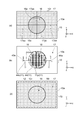
- FIG. 2A to FIG. 2C are schematic plan views illustrating the light emitting device according to the first embodiment.
- FIG. 2A is a plan view illustrating the first main surface 10 a of the substrate 10.
- FIG. 2B is a plan view illustrating the pattern of the first metal layer 11.
- FIG. 2C is a plan view illustrating the pattern of the second metal layer 12.
- FIG. 3A to FIG. 3C are plan views illustrating the light emitting device according to the first embodiment.
- FIG. 3A is a plan view illustrating the pattern of the first metal layer 11.
- FIG. 3B is a cross-sectional view illustrating a part of a cross section taken along line A1-A2 of FIG.
- FIG. 3C is a cross-sectional view illustrating a part of a cross section taken along line B1-B2 of FIG.
- the substrate 10 includes a reflective layer 81.
- the substrate 10 includes a first region R1 and a second region R2.
- the first metal layer 11 is provided on the second region R2.
- the second region R2 corresponds to a part of the mounting region 16.
- the first region R1 is included in the mounting region 16.
- the first region R1 may be included in the peripheral region 17.
- the reflective layer 81 is provided on the substrate 10 (on the first main surface 10a).
- the reflective layer 81 is provided on the first region R1 of the substrate 10.
- the reflective layer 81 may be provided not only on the mounting region 16 but also on the peripheral region 17.
- the wiring layer (first metal layer 11) is provided on the second region R2.
- a part of the reflective layer 81 may be located on a part of the wiring layer.
- a part of the wiring layer may be located on a part of the reflective layer 81.
- the substrate 10 and the reflective layer 81 may be chemically bonded through oxygen, for example. Thereby, high joint strength is obtained.
- the reflective layer 81 has glass (SiO 2 ) as a main component. That is, the reflective layer 81 includes a glass portion 81a. For this reason, the reflective layer 81 is not easily deteriorated by heat or light.
- the reflective layer 81 includes, for example, a ceramic filler 81b of zirconium oxide (for example, ZrO 2 ). Thereby, in the reflective layer 81, for example, a higher reflectance than that of a commonly used white ceramic substrate made of Al 2 O 3 can be obtained.
- the reflective layer 81 a highly stable glass (SiO 2 ) is used, and a ceramic filler 81 b having a refractive index different from that of the glass (SiO 2 ) is dispersed therein, thereby obtaining a high reflectance. It is done.
- the average value of the total light reflectance of the reflective layer 81 is, for example, 85% or more. More preferably, it is 92% or more.
- the total light reflectance is the sum of regular reflectance and diffuse reflectance. For example, a wavelength of 380 nm (nanometers) to 780 nm is targeted. In this way, a total light reflectance of 94% is obtained in the reflective layer 81.
- the thermal conductivity of the reflective layer 81 is 0.5 W / (m ⁇ K) or more and 3 W / (m ⁇ K) or less, for example, a total light reflectance of 94% is obtained in the reflective layer 81.
- the withstand voltage of the reflective layer 81 is, for example, not less than 0.2 kV and not more than 7 kV. More preferably, it is 0.5 kV or more and 5 kV or less. In the reflective layer 81, a total light reflectance of 94% is obtained.
- the thickness t81 of the reflective layer 81 is, for example, 20 ⁇ m or more and 120 ⁇ m or less. More preferably, it is 40 ⁇ m or more and 110 ⁇ m or less. In the reflective layer 81, a total light reflectance of 94% is obtained.
- the light emitting module substrate (mounting substrate portion 15) includes the base material (substrate 10) including at least one of aluminum oxide, aluminum nitride, and silicon nitride, and the first region R1 of the base material. It includes a reflective layer 81 provided on top and a wiring layer (such as the first metal layer 11) provided on the second region R2 of the base material.
- the substrate 10 high conductivity is obtained.
- the reflective layer 81 high reliability and high reflectance are obtained. According to the embodiment, a decrease in efficiency due to heat can be suppressed, and high light extraction efficiency can be obtained.
- a substrate for a light emitting module and a light emitting module capable of improving efficiency can be provided.
- a reflective layer 81 including a glass portion 81a and a ceramic filler 81b is used. Thereby, deterioration by heat and light can be suppressed, and high reliability can be obtained. In the embodiment, high light extraction efficiency due to high reflectance and high reliability are provided.
- the first metal layer 11 is provided on the first main surface 10a.
- the first metal layer 11 includes a plurality of mounting patterns 11p.
- the plurality of mounting patterns 11 p are provided in the mounting area 16. At least any two of the plurality of mounting patterns 11p are separated from each other. For example, at least one of the plurality of mounting patterns 11p has an island shape. Two of the plurality of mounting patterns 11p are independent of each other.
- the plurality of mounting patterns 11p include, for example, a first mounting pattern 11pa and a second mounting pattern 11pb.
- Each of the plurality of mounting patterns 11p includes, for example, a first mounting portion 11a and a second mounting portion 11b.
- the mounting pattern 11p further includes a third mounting portion 11c.
- the third mounting portion 11c is provided between the first mounting portion 11a and the second mounting portion 11b, and connects the first mounting portion 11a and the second mounting portion 11b. Examples of these mounting parts will be described later.
- the first metal layer 11 may further include a connection portion 44 that connects the plurality of mounting patterns 11p to each other.
- the first metal layer 11 further includes a first connector electrode portion 45e and a second connector electrode portion 46e.
- the first connector electrode portion 45e is electrically connected to one of the plurality of mounting patterns 11p.
- the second connector electrode portion 46e is electrically connected to one of the plurality of mounting patterns 11p other than the one.
- a semiconductor light emitting element is disposed on a part of one mounting pattern 11p. By this semiconductor light emitting element, the first connector electrode portion 45e is electrically connected to one of the mounting patterns 11p. Further, a semiconductor light emitting element is disposed on a part of another mounting pattern 11p. By this semiconductor light emitting element, the second connector electrode portion 46e is electrically connected to one of the other mounting patterns 11p.
- An example of the first metal layer 11 will be described later.
- the light emitting unit 40 further includes a first connector 45 and a second connector 46 provided on the first main surface 10a.
- the first connector 45 is electrically connected to the first connector electrode portion 45e.
- the second connector 46 is electrically connected to the second connector electrode portion 46e.
- the first connector 45 is provided on the first connector electrode portion 45e.
- a second connector 46 is provided on the second connector electrode portion 46e.
- the light emitting element portion 35 is disposed between the first connector 45 and the second connector 46. Electric power is supplied to the light emitting unit 40 via these connectors.
- the second metal layer 12 is provided on the second major surface 10b.
- the second metal layer 12 is electrically insulated from the first metal layer 11. At least a part of the second metal layer 12 overlaps the mounting region 16 when projected onto the XY plane (a first plane parallel to the first major surface 10a).
- the first metal layer 11 is provided on the upper surface (first main surface 10a) of the substrate 10
- the second metal layer 12 is provided on the lower surface (second main surface 10b) of the substrate 10.
- the light emitting element portion 35 is provided on the first main surface 10 a of the substrate 10.
- the light emitting element unit 35 includes a plurality of semiconductor light emitting elements 20 and a sealing layer 30.
- the upper surface 35u of the light emitting element unit 35 is, for example, a plane.
- a wavelength conversion layer 31 is used as the sealing layer 30.
- the plurality of semiconductor light emitting elements 20 are provided on the first major surface 10a. Each of the plurality of semiconductor light emitting elements 20 emits light.
- the semiconductor light emitting element 20 includes, for example, a nitride semiconductor.
- the semiconductor light emitting element 20 includes, for example, In y Al x Ga 1-xy N (0 ⁇ x ⁇ 1, 0 ⁇ y ⁇ 1, x + y ⁇ 1). However, in the embodiment, the semiconductor light emitting element is arbitrary.
- the plurality of semiconductor light emitting elements 20 include, for example, a first semiconductor light emitting element 20a and a second semiconductor light emitting element 20b. Each of the plurality of semiconductor light emitting elements 20 is electrically connected to any one of the plurality of mounting patterns 11p and another mounting pattern 11p adjacent to any one of the plurality of mounting patterns 11p. It is connected to the.
- the first semiconductor light emitting element 20a is electrically connected to the first mounting pattern 11pa and the second mounting pattern 11pb among the plurality of mounting patterns 11p.
- the second mounting pattern 11pb corresponds to another mounting pattern 11p adjacent to the first mounting pattern 11pa.
- each of the plurality of semiconductor light emitting elements 20 includes a first semiconductor layer 21 of a first conductivity type, a second semiconductor layer 22 of a second conductivity type, and a light emitting layer 23.
- the first conductivity type is n-type and the second conductivity type is p-type.
- the first conductivity type may be p-type and the second conductivity type may be n-type.
- the first semiconductor layer 21 includes a first portion (first semiconductor portion 21a) and a second portion (second semiconductor portion 21b).
- the second semiconductor portion 21b is aligned with the first semiconductor portion 21a in a direction (for example, the X-axis direction) intersecting with the stacking direction (Z-axis direction from the heat dissipation member 51 toward the light emitting unit 40).
- the second semiconductor layer 22 is provided between the second semiconductor portion 21 b and the mounting substrate unit 15.
- the light emitting layer 23 is provided between the second semiconductor portion 21 b and the second semiconductor layer 22.
- the semiconductor light emitting element 20 is, for example, a flip chip type light emitting element.
- the first semiconductor portion 21a of the first semiconductor layer 21 faces the first mounting portion 11a of the mounting pattern 11p.
- the second semiconductor layer 22 faces the second mounting portion 11b of the mounting pattern 11p.
- the first semiconductor portion 21a of the first semiconductor layer 21 is electrically connected to the first mounting portion 11a.
- the second semiconductor layer 22 is electrically connected to the second mounting portion 11b.
- solder or gold bumps are used. This connection is performed by, for example, metal fusion solder bonding. Alternatively, this connection is performed by, for example, an ultrasonic thermocompression method using gold bumps.
- the light emitting element unit 35 further includes a first bonding metal member 21e and a second bonding metal member 22e.
- the first bonding metal member 21e is provided between the first semiconductor portion 21a and one of the mounting patterns 11p (for example, the first mounting portion 11a).
- the second bonding metal member 22e is provided between the second semiconductor layer 22 and another mounting pattern 11p (for example, the second mounting pattern 11pb).
- At least one of the first bonding metal member 21e and the second bonding metal member 22e includes solder or gold bumps.
- the cross-sectional areas (the cross-sectional areas when cut along the XY plane) of the first bonding metal member 21e and the second bonding metal member 22e can be increased.
- heat can be efficiently transmitted to the mounting substrate portion 15 via the first bonding metal member 21e and the second bonding metal member 22e, and heat dissipation is improved.
- the wavelength conversion layer 31 covers at least a part of the plurality of semiconductor light emitting elements 20.
- the wavelength conversion layer 31 absorbs at least part of light (for example, first light) emitted from the plurality of semiconductor light emitting elements 20 and emits second light.
- the wavelength (for example, peak wavelength) of the second light is different from the wavelength (for example, peak wavelength) of the first light.
- the wavelength conversion layer 31 includes, for example, a plurality of wavelength conversion particles such as a phosphor and a light transmissive resin in which the plurality of wavelength conversion particles are dispersed.
- the first light includes, for example, blue light.
- the second light includes light having a longer wavelength than the first light.
- the second light includes, for example, at least one of yellow light and red light.
- the light transmissive resin of the wavelength conversion layer 31 for example, a silicone resin is used.
- a light transmissive inorganic material such as glass (SiO 2 ) may be used.
- the light emitting element portion 35 further includes a light reflective wall portion 32.
- the wall portion 32 surrounds the wavelength conversion layer 31 in the XY plane.
- the wall portion 32 includes, for example, a plurality of particles such as a metal oxide and a light transmissive resin in which the particles are dispersed. Particles such as metal oxides have light reflectivity. For example, at least one of TiO 2 and Al 2 O 3 can be used as the particles of the metal oxide.
- the light emitting unit 40 is, for example, a chip-on-board (COB) type LED module.
- COB chip-on-board
- the luminous flux divergence of the light emitted from the light emitting element unit 35 is not less than 10 lumen / square millimeter (lm / mm 2 ) and not more than 100 lumen / square millimeter. Desirably, it is 20 lumens / square millimeter or more. That is, in this embodiment, the ratio (light flux divergence) of the light emitted from the light emitting element portion 35 to the light emitting area is very high. In the present specification, the light emitting area substantially corresponds to the area of the mounting region 16.
- the light emitting device 110 is used for, for example, a projector.
- the light emitting device 110 is disposed on the lighting device member 71, for example.
- the illumination device member 71 is omitted.
- the lighting device member 71 is a part of the lighting device.
- a lighting device connection member 53 is provided between the lighting device member 71 and the light emitting device 110.
- solder or grease is used for the lighting device connecting member 53.
- the heat of the light emitting device 110 is conducted to the lighting device member 71 by the lighting device connecting member 53 to be radiated.
- FIGS. 1A and 1B also illustrate an example of a configuration of a lighting device 210 (lighting fixture) including the light-emitting device 110.
- the lighting device 210 includes a lighting device member 71 and a light emitting device 110.
- the light emitting device 110 is provided on the lighting device member 71.
- the lighting device 210 may further include a lighting device connection member 53.
- the lighting device connecting member 53 is provided between the lighting device member 71 and the light emitting device 110, and is in contact with the heat radiating member 51 of the light emitting device 110 and the lighting device member 71.
- the lighting device connection member 53 may be included in the light emitting device 110.
- the heat radiating member 51 when the heat radiating member 51 is projected on the XY plane (first plane), the heat radiating member 51 has an area that is five times or more the area of the mounting region 16.
- the area of the heat dissipation member 51 is set to be very large with respect to the area of the mounting region 16.
- the heat generated in the light emitting element portion 35 provided on the mounting region 16 is spread in the in-plane direction (XY in-plane direction) by the heat radiating member 51 having a large area.
- the heat which spread in the in-plane direction is transmitted toward the illuminating device member 71 to which the light-emitting device 110 is attached, for example, and is thermally radiated efficiently.
- the first main surface 10 a includes a mounting region 16 and a peripheral region 17.
- the pattern of the mounting area 16 is substantially circular.
- the center of the mounting region 16 is provided so as to substantially coincide with the center of the substrate 10.
- the peripheral area 17 is an area around the mounting area 16.
- the area of the peripheral region 17 is larger than the area of the mounting region 16.
- the area of the peripheral region 17 is four times or more the area of the mounting region 16.
- the area of the peripheral region 17 is preferably 9 times or less the area of the mounting region 16.
- the distance between them (shortest distance) is not less than 1 ⁇ 2 of the width of the mounting region 16 along the direction passing through the center (X-axis direction).
- the distance 17xa (shortest distance) between the outer edge 10r along the X-axis direction and the mounting region 16 is 1 ⁇ 2 or more of the width 16x of the mounting region 16.
- the distance 17xb (shortest distance) between the outer edge 10r along the X-axis direction and the mounting region 16 is 1 ⁇ 2 or more of the width 16x of the mounting region 16.
- the distance 17ya (shortest distance) between the outer edge 10r along the Y-axis direction and the mounting region 16 is 1 ⁇ 2 or more of the width 16y of the mounting region 16.
- the distance 17 yb (shortest distance) between the outer edge 10 r along the Y-axis direction and the mounting region 16 is 1 ⁇ 2 or more of the width 16 y of the mounting region 16.
- the area of the peripheral region 17 becomes larger than the area of the mounting region 16.
- the generated heat is efficiently spread along the in-plane direction. Thereby, heat dissipation increases.
- the plurality of mounting patterns 11 p that are part of the first metal layer 11 are provided in the mounting region 16.
- the plurality of mounting patterns 11p are provided in a circular area.
- the mounting area 16 is an area containing a plurality of mounting patterns 11p when projected onto the XY plane.
- a region between the plurality of mounting patterns 11 p is included in the mounting region 16.
- the inner side of the line connecting the outer edges of the mounting patterns 11p arranged on the outer side among the plurality of mounting patterns 11p is the mounting region 16.
- the plurality of mounting patterns 11p are arranged in a substantially circular region, for example.
- a substantially circular area containing a plurality of mounting patterns 11p may be practically used as the mounting area 16.
- the mounting area 16 includes an area where a plurality of mounting patterns 11p are provided when projected onto the XY plane.
- the mounting area 16 does not include an area where the connection portion 44, the first connector electrode portion 45e, and the second connector electrode portion 46e are provided when projected onto the XY plane. This area is included in the peripheral area 17.
- some of the plurality of mounting patterns 11p are independent of each other. Two independent mounting patterns 11p adjacent to each other are electrically connected by a semiconductor light emitting element 20 disposed thereon. Some of the plurality of semiconductor light emitting elements 20 are connected in series, for example. The plurality of semiconductor light emitting elements 20 connected in series are arranged, for example, along the X-axis direction.
- two of the plurality of mounting patterns 11p are connected by the connecting portion 44.
- the group of the several semiconductor light emitting element 20 connected in series is further connected.
- a group of a plurality of semiconductor light emitting elements arranged in series along the X axis are arranged in the Y axis direction.
- a group of a plurality of semiconductor light emitting elements connected in series are connected in parallel to each other.
- the mounting pattern 11p is electrically connected to the first connector electrode portion 45e or the second connector electrode portion 46e via the wiring pattern 44c.
- a current is supplied to the mounting pattern 11p via the first connector 45 provided on the first connector electrode portion 45e and the second connector 46 provided on the second connector electrode portion 46e. The The current is supplied to the semiconductor light emitting element 20, and light is generated.
- the area of the second metal layer 12 is designed to be large.
- the area of the second metal layer 12 is larger than the area of the mounting region 16.
- the area of the second metal layer 12 projected onto the XY plane (the first plane parallel to the stacking direction) is 95% or more of the area of the second major surface 10b. Increasing the area of the second metal layer 12 increases the efficiency of heat dissipation.
- the planar pattern of the heat conductive layer 52 is substantially along the pattern of the second metal layer 12.
- the area of the heat conductive layer 52 can be increased. Thereby, the efficiency of heat conduction through the heat conductive layer 52 can be improved.
- the outer edge 12r of the second metal layer 12 when projected onto the XY plane (first plane) is located outside the outer edge 16r of the mounting region 16.
- the area of the second metal layer 12 when projected onto the XY plane (first plane) may be smaller than the area of the mounting region 16. Also in this case, the area of the second metal layer 12 when projected onto the XY plane (first plane) is larger than 80% of the area of the mounting region 16. If it is smaller than this, the efficiency of heat dissipation becomes low.
- FIG. 4 is a schematic cross-sectional view illustrating the light emitting device according to the first embodiment.
- FIG. 4 illustrates a part of the light emitting unit 40.
- the first metal layer 11 includes a copper film 13a (Cu film).
- the first metal layer 11 may further include a metal film 13d (Rh layer).
- the copper film 13 a is provided between the metal film 13 d and the substrate 10.
- the first metal layer 11 includes a nickel film 13b (Ni film) provided between the copper film 13a and the metal film 13d, and a palladium film 13c provided between the nickel film 13b and the metal film 13d. (Pd film).
- the first metal layer 11 has a stacked structure of Cu / Ni / Pd / Rh.
- the first bonding metal member 21e and the second bonding metal member 22e are in contact with the metal film 13d.
- the metal film 13 d is located on the outermost surface of the first metal layer 11.
- Au may be used as the metal film 13d.
- the first metal layer 11 includes, for example, a metal film 13d containing at least one of gold (Au) and rhodium (Rh).
- Au gold
- Rh rhodium
- an alloy material including at least one of Au and rhodium (Rh) may be used for the metal film 13d. Thereby, the reflectance of the first metal layer 11 is improved.
- the thickness of the metal film 13d is preferably 0.15 ⁇ m or more and 0.25 ⁇ m. Thereby, a high reflectance is obtained.
- the second metal layer 12 includes a copper film 14a.
- the second metal layer 12 may further include a metal film 14d (gold film).
- the copper film 14 a is provided between the metal film 14 d and the substrate 10.
- the second metal layer 12 further includes a nickel film 14b provided between the copper film 14a and the metal film 14d, and a palladium film 14c provided between the nickel film 14b and the metal film 14d. Contains.
- the second metal layer 12 has a stacked structure of Cu / Ni / Pd / Au.
- the boundary between each of the copper film, nickel film, palladium film and metal film may not be clear.
- Some of these layers may have a mixed state (for example, an alloy state).
- the same material as that of the first metal layer 11 can be used.
- the same stacked structure as the stacked structure of the first metal layer 11 can be applied. Thereby, formation of these metal layers becomes easy.
- the configuration of the second metal layer 12 may be different from the configuration of the first metal layer 11.
- the thickness t11 of the first metal layer 11 is, for example, 30 ⁇ m or more and 100 ⁇ m or less, for example, 40 ⁇ m or more and 60 ⁇ m or less.
- the thickness t12 of the second metal layer 12 is, for example, 30 ⁇ m or more and 100 ⁇ m or less, for example, 40 ⁇ m or more and 60 ⁇ m or less.
- the copper film 13a of the first metal layer 11 and the copper film 14a of the second metal layer 12 can be formed by, for example, electrolytic plating.
- Each of the thickness of the copper film 13a and the thickness of the copper film 14a is, for example, 30 ⁇ m or more and 100 ⁇ m or less, for example, about 50 ⁇ m.
- the nickel film 13b, the palladium film 13c, and the metal film 13d are formed by, for example, electroless plating.
- the nickel film 14b, the palladium film 14c, and the metal film 14d are formed by, for example, electrolytic plating.
- Each of the thickness of the nickel film 13b and the thickness of the nickel film 14b is, for example, not less than 2 ⁇ m and not more than 8 ⁇ m, for example, about 4.5 ⁇ m.
- Each of the thickness of the palladium film 13c and the thickness of the palladium film 14c is, for example, not less than 0.075 ⁇ m and not more than 0.2 ⁇ m, for example, about 1 ⁇ m.
- the thickness of the metal film 13d is 0.15 ⁇ m or more and 0.25 ⁇ m or less when Rh is used.
- the thickness of the metal film 13d is 0.05 ⁇ m or more and 0.2 ⁇ m or less when Au is used.
- the thickness of the metal film 14d is, for example, about 0.1 ⁇ m.
- the side surface of the first metal layer 11 and the side surface of the second metal layer 12 are Can be substantially vertical.
- the side surface 11s of the first metal layer 11 when cut along a plane perpendicular to the first main surface 10a is in the stacking direction (Z-axis direction). Can be made almost parallel.
- the angle ⁇ between the side surface 11s of the first metal layer 11 and the first main surface 10a is, for example, not less than 80 degrees and not more than 95 degrees.
- the angle ⁇ is more preferably 85 degrees or more.
- the angle ⁇ is small, the area of the lower surface of the mounting pattern 11p is excessive with respect to the area for mounting the mounting pattern 11p that is a part of the first metal layer 11 (for example, the area of the upper surface). It gets bigger. For this reason, the ratio of the part covered with the mounting pattern 11p among the upper surfaces (the 1st main surface 10a) of the board
- first main surface 10a Mounting on the upper surface (first main surface 10a) of the substrate 10 by setting the angle ⁇ between the side surface 11s of the first metal layer 11 and the first main surface 10a to 80 degrees or more and 95 degrees or less.
- the ratio of the portion covered with the pattern 11p can be reduced. Thereby, the reflectance as the whole mounting region 16 can be made sufficiently high. Thereby, the luminous flux divergence can be improved.
- the curvature of the corner portion of the cross section of the first metal layer 11 is relatively high. That is, the radius of curvature is small.
- the cross section of the first metal layer 11 is close to a rectangle, that is, the side surface 11s is close to vertical.
- the first metal layer 11 further includes an upper surface 11u parallel to the XY plane (first plane).
- the radius of curvature of the corner portion 11su that connects the upper surface 11u of the first metal layer 11 and the side surface 11s of the first metal layer 11 is 10 ⁇ m or less.
- the area of the lower surface of the mounting pattern 11p can be made smaller than the area for mounting the mounting pattern 11p (for example, the area of the upper surface 11u of the mounting pattern 11p).
- region 16 can be made high, and luminous flux divergence can be improved.
- a part of the wavelength conversion layer 31 is disposed at a position 11g (space) between any one of the plurality of semiconductor light emitting elements 20 and the substrate 10.
- the position 11g is a position between any one of the mounting patterns 11p (for example, the first mounting pattern 11pa) and another mounting pattern 11p (for example, the second mounting pattern 11pb).
- the first light emitted from the semiconductor light emitting element 20 can be efficiently converted into the second light by the wavelength conversion layer 31.
- a wavelength conversion member containing a transparent resin or another phosphor material may be separately arranged.
- a space including the position 11g may be enlarged.
- the gap between the semiconductor light emitting element 20 and the substrate 10 is increased.
- the distance tg between any of the plurality of semiconductor light emitting elements 20 and the substrate 10 along the Z-axis direction is set to be relatively long.
- the distance tg is 1/10 or more of the thickness t20 (height) along the Z-axis direction of the plurality of semiconductor light emitting elements 20.
- the height of the semiconductor light emitting element 20 is, for example, not less than 50 ⁇ m and not more than 500 ⁇ m, for example, 300 ⁇ m.
- the distance tg is, for example, not less than 40 ⁇ m and not more than 110 ⁇ m, for example, 60 ⁇ m.
- the thickness t10 of the substrate 10 is, for example, not less than 0.3 mm and not more than 2 mm, for example, 0.635 mm. If the thickness t10 of the substrate 10 is less than 0.3 mm, for example, the mechanical strength of the substrate 10 becomes weak. When the thickness t10 of the substrate 10 exceeds 2 mm, for example, the efficiency of conduction of heat generated in the semiconductor light emitting element 20 (light emitting element portion 35) to the heat radiating member 51 becomes low.
- the wavelength conversion layer 31 includes a plurality of wavelength conversion particles 31a such as a phosphor, and a light transmissive resin 31b in which the plurality of wavelength conversion particles 31a are dispersed.
- the wavelength conversion particle 31a absorbs at least a part of the first light emitted from the plurality of semiconductor light emitting elements 20, and emits second light having a wavelength different from the wavelength of the first light.
- the light emitting device can be used as an illumination device such as a projector.
- FIG. 5A to FIG. 5C are schematic views illustrating the light emitting module substrate according to the first embodiment.
- the light emitting module substrate 15a according to this embodiment includes a base material 10S (for example, the substrate 10 described above), a reflective layer 81, and a wiring layer 11L (the first metal layer 11 described above). ) And.
- the base material 10S is electrically insulating.
- the reflective layer 81 is provided on at least a part of the base material 10S.
- the reflective layer 81 includes a plurality of fine structures 81c and a silicon oxide portion 81d.
- the silicon oxide portion 81d is provided around at least a part of the plurality of microstructures 81c.
- the wiring layer 11L is provided on at least a part of the base material 10S.
- the fine structure 81c includes, for example, zirconium oxide.
- the fine structure 81c may include, for example, aluminum oxide.
- Silicon oxide unit 81d includes, for example, SiO 2.
- the silicon oxide part 81d is, for example, a glass part 81a.
- the fine structure 81c is, for example, a ceramic filler 81b.
- At least a part of the reflective layer 81 is between at least a part of the base material 10S and at least a part of the wiring layer 11L. Located in.
- At least a part of the wiring layer 1L is between at least a part of the base material 10S and at least a part of the reflective layer 81. Located in.
- substrate for light emitting modules which can improve efficiency can be provided.
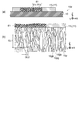
- FIG. 6A and FIG. 6B are schematic cross-sectional views illustrating the light emitting module substrate according to the second embodiment.
- FIG. 6B illustrates a part of the base material 10 ⁇ / b> S illustrated in FIG.
- the light emitting module substrate 15d also includes an electrically insulating base material 10S, a reflective layer 81, and a wiring layer 11L.
- the reflective layer 81 is provided on at least a part of the substrate 10S.
- the reflective layer 81 includes a plurality of microstructures 81c and a silicon oxide portion 81d provided around at least a part of the plurality of microstructures 81c.
- the wiring layer 11L is provided on at least a part of the base material 10S.
- the wiring layer 11L is, for example, the first metal layer 11.
- the base material 10S includes a polycrystal 10p.
- the polycrystal 10p includes a plurality of grains 10pg.
- the base material 10S includes a plurality of grain boundaries 10gb.
- Grains 10 pg are located between the plurality of grain boundaries 10 gb.
- Grain 10pg is divided by the grain boundary 10gb.
- the grain 10 pg has, for example, at least a partial structure of hexagonal crystal.
- the base material 10S includes at least one of aluminum oxide, aluminum nitride, and silicon nitride.
- the base material 10S includes, for example, silicon nitride.
- the orientation of the polycrystal 10p is along the Z-axis direction (first direction from the substrate 10S toward the reflective layer 81).
- the first length GL1 along one Z-axis direction (first direction) of the polycrystal 10p is polycrystal along the X-axis direction (second direction perpendicular to the first direction). It is longer than one second length GL2 of 10p.
- the first length GL1 along one Z-axis direction (first direction) of the plurality of grains 10pg included in the polycrystal 10p is, for example, in the X-axis direction (second direction perpendicular to the first direction). It is longer than one second length GL2 of the plurality of grains 10pg included along the polycrystalline 10p.
- the second length GL2 may be one length in the XY plane.
- 1st length GL1 of one grain 10pg is 0.3 micrometer or more and 30 micrometers or less, for example.
- the second length GL2 of one grain 10pg is, for example, not less than 0.3 ⁇ m and not more than 5 ⁇ m.
- the aspect ratio is 0.5 or more and 10 or less.
- the aspect ratio is a ratio of one first length GL1 of the plurality of grains 10pg included in the polycrystal 10p to one second length GL2 of the plurality of grains 10pg included in the polycrystal 10p.
- the first length GL1 is, for example, not less than 0.6 ⁇ m and not more than 30 ⁇ m
- the second length GL2 is, for example, not less than 0.3 ⁇ m and not more than 5 ⁇ m.
- the average of the second lengths GL2 of the plurality of grains 10pg is, for example, not less than 0.6 ⁇ m and not more than 3 ⁇ m.
- the second length GL2 of each of the plurality of grains 10pg is, for example, not less than 0.3 ⁇ m and not more than 24 ⁇ m.
- the standard deviation of the second length GL2 of each of the plurality of grains 10pg is 3 ⁇ m or less. The standard deviation may be 0.3 ⁇ m or more, for example.
- the base material 10S includes a portion of the polycrystal 10p, and the polycrystal 10p is substantially oriented along the Z-axis direction.
- the full width at half maximum of the polycrystal 10p is, for example, 10 degrees or less.
- the adhesion between the substrate 10S and the reflective layer 81 is increased.
- the polycrystal 10p is substantially oriented along the Z-axis direction, so that the size of the grains 10pg on the upper surface of the substrate 10S (the surface on the reflective layer 81 side of the substrate 10S) is This is considered to be because the length of GL2 becomes 2 and the size of the grains 10pg becomes uniform on the upper surface of the substrate 10S.
- the difference in thermal expansion coefficient is within 10% on the upper surface of the base material 10S. Thereby, it can suppress that the reflection layer 81 peels from the base material 10S by the stress resulting from the difference in size of the grain 10pg being large.
- Such a base material 10S can be obtained, for example, by applying a magnetic field to the material to be the base material 10S in the manufacturing process.
- a magnetic field for example, the orientation of the crystal grains of the material to be the base material 10S can be aligned by the magnetic field.
- the size of the grains 10pg is not uniform on the upper surface of the substrate 10S.
- the size of the grains 10pg is not uniform on the upper surface of the substrate 10S.
- the thermal expansion coefficient is different between the grain portion of 10 pg and the grain boundary portion of 10 gb.
- the bonding is performed at a portion where the difference in the thermal expansion coefficient is large when there is a temperature change. It is thought that stress is generated. For this reason, if the size of the grains 10pg is not uniform on the upper surface of the base material 10S, peeling may occur between the base material 10S and the reflective layer 81.
- the polycrystal 10p of the base material 10S is oriented substantially along the Z-axis direction. Therefore, on the upper surface of the base material 10S, the size of the grain 10pg is as described above. Uniform compared to the reference example. Thereby, it is considered that peeling is suppressed between the base material 10 ⁇ / b> S and the reflective layer 81.
- the reflective layer 81 when peeling occurs in the reflective layer 81, it is difficult to obtain desired reflection characteristics. Reliability is also reduced. According to the present embodiment, it is possible to provide a light emitting module substrate that can stably improve the efficiency.
- the polycrystal 10p of the base material 10S is substantially oriented along the Z-axis direction, heat conduction along the Z-axis direction is efficiently performed.
- the thermal conductivity is about 85 W / (m ⁇ K).
- the thermal conductivity is about 150 W / (m ⁇ K).
- FIG. 7 is a schematic plan view illustrating the light emitting device and the lighting device according to the second embodiment.
- the base material 10S has a hole 10Sh.
- the hole 10Sh extends, for example, in the Z-axis direction (first direction).
- the hole 10Sh penetrates the base material 10S, for example.
- the base 10S (that is, the light emitting module substrate 15d) can be separately fixed to the member using the hole 10Sh.
- the processing for forming the hole 10Sh along the Z-axis direction becomes easy. Thereby, the shape of the hole 10Sh is stabilized.
- the thickness of the base material 10S is not less than 0.3 mm and not more than 2 mm.
- a highly accurate hole 10Sh can be formed in the substrate 10S having such a thickness.
- the base material 10S preferably includes, for example, silicon nitride.
- the strength of silicon nitride is 600 MPa to 700 MPa, and the fracture toughness value indicating crack extension is 6 MPa (m) 1/2 to 7 MPa (m) 1/2, which is relatively high. Silicon nitride has a relatively high toughness. For this reason, it becomes easy to obtain the hole 10Sh with higher accuracy. Furthermore, the shape of the hole 10Sh can be prevented from changing during use.
- the reflective layer 81 is preferably separated from the hole 10Sh of the base material 10S. That is, it is preferable not to provide the reflective layer 81 around the hole 10Sh.
- the reflective layer 18 is close to the hole 10Sh, when a fixing member such as a screw is inserted into the hole 81Sh, the fixing member may crack in the reflective layer 81, and reliability may be reduced.
- the fixing member may crack in the reflective layer 81, and reliability may be reduced.
- a light emitting module substrate, a light emitting module, and a lighting fixture that can improve efficiency are provided.
- vertical and parallel include not only strictly vertical and strictly parallel, but also include, for example, variations in the manufacturing process, and may be substantially vertical and substantially parallel. is good.
- a light emitting part a mounting substrate part, a light emitting element part, a light emitting module substrate, a first metal layer, a second metal layer, a semiconductor light emitting element, a wavelength conversion layer, a wall part, a heat radiating member, a heat conduction layer included in the light emitting device
- the present invention is similarly implemented by appropriately selecting from a known range by those skilled in the art, and the same effect is obtained. As long as it can be obtained, it is included in the scope of the present invention.
Landscapes
- Led Device Packages (AREA)
Abstract
実施形態によれば、基材と、反射層と、配線層と、を含む発光モジュール用基板が提供される。前記基材は、電気絶縁性である。前記反射層は、前記基材の少なくとも一部の上に設けられ、複数の微細構造体と、前記複数の微細構造体の少なくとも一部の周りに設けられた酸化ケイ素部と、を含む。前記配線層は、前記基材の少なくとも一部の上に設けられる。
Description
本発明の実施形態は、発光モジュール用基板、発光モジュール及び照明器具に関する。
例えば、青色光を発光する半導体発光素子と、光の波長を変換する蛍光体と、を組み合わせて白色光を発光する発光装置(LEDモジュール)がある。このような発光装置は、投光器などの照明装置などに応用できる。発光装置において、効率の向上が求められる。LEDモジュールに用いられる基板において、効率を向上することが求められる。
本発明の実施形態は、効率を向上できる発光モジュール用基板、発光モジュール及び照明器具を提供する。
本発明の実施形態によれば、基材と、反射層と、配線層と、を含む発光モジュール用基板が提供される。前記基材は、電気絶縁性である。前記反射層は、前記基材の少なくとも一部の上に設けられ、複数の微細構造体と、前記複数の微細構造体の少なくとも一部の周りに設けられた酸化ケイ素部と、を含む。前記配線層は、前記基材の少なくとも一部の上に設けられる。
本発明の実施形態によれば、効率を向上できる発光モジュール用基板、発光モジュール及び照明器具が提供される。
以下に、本発明の各実施の形態について図面を参照しつつ説明する。
なお、図面は模式的または概念的なものであり、各部分の厚みと幅との関係、部分間の大きさの比率などは、必ずしも現実のものと同一とは限らない。また、同じ部分を表す場合であっても、図面により互いの寸法や比率が異なって表される場合もある。
なお、本願明細書と各図において、既出の図に関して前述したものと同様の要素には同一の符号を付して詳細な説明は適宜省略する。
なお、図面は模式的または概念的なものであり、各部分の厚みと幅との関係、部分間の大きさの比率などは、必ずしも現実のものと同一とは限らない。また、同じ部分を表す場合であっても、図面により互いの寸法や比率が異なって表される場合もある。
なお、本願明細書と各図において、既出の図に関して前述したものと同様の要素には同一の符号を付して詳細な説明は適宜省略する。
(第1の実施形態)
図1(a)及び図1(b)は、第1の実施形態に係る発光装置及び照明装置を例示する模式図である。
図1(a)は平面図である。図1(b)は、図1(a)のA1-A2線断面の一部を例示する断面図である。
図1(a)及び図1(b)に表したように、本実施形態に係る発光装置110(発光モジュール)は、発光部40と、放熱部材51と、熱伝導層52と、を含む。
図1(a)及び図1(b)は、第1の実施形態に係る発光装置及び照明装置を例示する模式図である。
図1(a)は平面図である。図1(b)は、図1(a)のA1-A2線断面の一部を例示する断面図である。
図1(a)及び図1(b)に表したように、本実施形態に係る発光装置110(発光モジュール)は、発光部40と、放熱部材51と、熱伝導層52と、を含む。
放熱部材51の上に、発光部40が設けられる。放熱部材51と発光部40との間に、熱伝導層52が設けられる。
すなわち、放熱部材51の上に熱伝導層52が設けられ、熱伝導層52の上に、発光部40が設けられる。この例では、放熱部材51の上に1つの発光部40が設けられる。後述するように、1つの放熱部材51の上に、複数の発光部40が設けられても良い。
本願明細書において、上に設けられる状態は、直接的に上に設けられる状態の他に、間に別の要素が挿入される状態も含む。
放熱部材51から発光部40に向かう方向を積層方向とする。本願明細書において、積層される状態は、直接接して重ねられる状態の他に、間に別の要素が挿入されて重ねられる状態も含む。
積層方向をZ軸方向とする。Z軸方向に対して垂直な1つの軸をX軸方向とする。Z軸方向に対して垂直で、X軸方向に対して垂直な方向をY軸方向とする。
図1(b)に表したように、放熱部材51は、例えば板状である。放熱部材51の主面は、例えば、X-Y平面に対して実質的に平行である。放熱部材51の平面形状は、例えば矩形である。放熱部材51は、例えば、第1~第4辺55a~55dを有する。第2辺55bは、第1辺55aから離間する。第3辺55cは、第1辺55aの一端と、第2辺55bの一端と、を接続する。第4辺55dは、第3辺55cと離間し、第1辺55aの他端と、第2辺55bの他端と、を接続する。放熱部材51の平面形状のコーナー部は、曲線状でも良い。放熱部材51の平面形状は、矩形でなくても良く、任意である。放熱部材51の縁部51rは、例えば、曲線状でも良い。
放熱部材51には、例えば、金属などの基板が用いられる。放熱部材51には、例えば、銅やアルミニウムなどが用いられる。
発光部40は、光を放出する。それと同時に、発光部40は熱を発生する。熱伝導層52は、発光部40で発生した熱を、放熱部材51に効率良く伝導する。熱伝導層52には、例えば、はんだなどが用いられる。すなわち、熱伝導層52は、はんだを含む。この場合、熱伝導層52は、発光部40と放熱部材51とを接合する。熱伝導層52の厚さt52は、例えば、10μm(マイクロメートル)以下である。
熱伝導層52には、液体状または固体状の潤滑油(グリース)などを用いても良い。熱伝導層52には、潤滑油(グリース)よりもさらに熱伝導率を高めるために、シリコーンにアルミナなどの金属粉末を混合した導電性を有する潤滑油(導電性グリース)などを用いても良い。
発光部40は、実装基板部15(発光モジュール用基板)と、発光素子部35と、を含む。
実装基板部15は、基板10と、第1金属層11と、第2金属層12と、を含む。
基板10は、電気的に絶縁性である。基板10には、例えば、セラミック基板などが用いられる。例えば、基板10は、酸化アルミニウム(例えばAl2O3)、窒化アルミニウム(例えば、AlN)及び窒化ケイ素(例えば、Si3N4)の少なくともいずれかを含む。基板10には、例えば、Al2O3、AlN、及びSi3N4の少なくともいずれかを主成分とするセラミック基板などが用いられる。
基板10は、第1主面10aと、第2主面10bと、を有する。第2主面10bは、第1主面10aとは反対側の面である。放熱部材51は、基板10の第2主面10bに対向している。換言すると、第2主面10bは、放熱部材51側の面である。
基板10は、電気的に絶縁性である。基板10には、例えば、セラミック基板などが用いられる。例えば、基板10は、酸化アルミニウム(例えばAl2O3)、窒化アルミニウム(例えば、AlN)及び窒化ケイ素(例えば、Si3N4)の少なくともいずれかを含む。基板10には、例えば、Al2O3、AlN、及びSi3N4の少なくともいずれかを主成分とするセラミック基板などが用いられる。
基板10は、第1主面10aと、第2主面10bと、を有する。第2主面10bは、第1主面10aとは反対側の面である。放熱部材51は、基板10の第2主面10bに対向している。換言すると、第2主面10bは、放熱部材51側の面である。
本願明細書において、対向している状態は、直接面している状態に加え、間に別の要素が挿入されている状態も含む。
第1主面10aは、実装領域16を含む。例えば、実装領域16は、第1主面10aの外縁10r(縁部10ue)から離間している。この例では、実装領域16は、第1主面10aの中央部分に設けられる。第1主面10aは、周辺領域17をさらに含む。周辺領域17は、実装領域16の周りに設けられる。
第1金属層11は、第1主面10aの側において、実装領域16の上に設けられる。一方、第2金属層12は、第2主面10bの側に設けられる。
実装基板部15の例の詳細は、後述する。
実装基板部15の例の詳細は、後述する。
図2(a)~図2(c)は、第1の実施形態に係る発光装置を例示する模式的平面図である。
図2(a)は、基板10の第1主面10aを例示する平面図である。図2(b)は、第1金属層11のパターンを例示する平面図である。図2(c)は、第2金属層12のパターンを例示する平面図である。
図2(a)は、基板10の第1主面10aを例示する平面図である。図2(b)は、第1金属層11のパターンを例示する平面図である。図2(c)は、第2金属層12のパターンを例示する平面図である。
図3(a)~図3(c)は、第1の実施形態に係る発光装置を例示する平面図である。
図3(a)は、第1金属層11のパターンを例示する平面図である。図3(b)は、図1(a)のA1-A2線断面の一部を例示す断面図である。図3(c)は、図3(a)のB1-B2線断面の一部を例示す断面図である。
図3(a)~図3(c)に表したように、基板10は、反射層81を含む。
図3(a)は、第1金属層11のパターンを例示する平面図である。図3(b)は、図1(a)のA1-A2線断面の一部を例示す断面図である。図3(c)は、図3(a)のB1-B2線断面の一部を例示す断面図である。
図3(a)~図3(c)に表したように、基板10は、反射層81を含む。
基板10は、第1領域R1と第2領域R2とを含む。第2領域R2の上に、第1金属層11が設けられる。第2領域R2は、実装領域16の一部に対応する。第1領域R1は、実装領域16に含まれる。第1領域R1は、周辺領域17に含まれても良い。
図3(a)~図3(c)に表したように、反射層81は、基板10の上(第1主面10aの上)に設けられる。例えば、反射層81は、基板10の第1領域R1の上に設けられる。反射層81は、実装領域16の上だけでなく、周辺領域17の上に設けられても良い。
一方、配線層(第1金属層11)は、第2領域R2の上に設けられる。配線層の一部の上に、反射層81の一部が位置しても良い。反射層81の一部の上に、配線層の一部が位置しても良い。
基板10と反射層81とは、例えば、酸素を介して化学結合されても良い。これにより、高い接合強度が得られる。
反射層81は、ガラス(SiO2)を主成分とする。すなわち、反射層81は、ガラス部81aを含む。このため、反射層81は、熱や光によって劣化しにくい。反射層81は、例えば、酸化ジルコニウム(例えば、ZrO2)のセラミックスフィラー81bを含む。これにより、反射層81において、例えば、一般的に使われるAl2O3からなる白色のセラミック基板よりも高い反射率が得られる。
反射層81において、安定性の高いガラス(SiO2)を用い、その中に、ガラス(SiO2)の屈折率とは異なる屈折率を有するセラミックスフィラー81bを分散することで、高い反射率が得られる。反射層81の全光線反射率の平均値は、例えば、85%以上である。92%以上であることが、さらに好ましい。全光線反射率は、正反射率と拡散反射率との和である。例えば、380nm(ナノメートル)以上780nm以下の波長を対象とする。このようにすることで、反射層81において、94%の全光線反射率が得られる。
反射層81の熱伝導率が、例えば、0.5W/(m・K)以上3W/(m・K)以下であるときに、反射層81において、94%の全光線反射率が得られる。
反射層81の耐電圧は、例えば、0.2kV以上7kV以下である。0.5kV以上5kV以下であることが、さらに好ましい。反射層81において、94%の全光線反射率が得られる。
反射層81の厚さt81は、例えば、20μm以上120μm以下である。40μm以上110μm以下であることが、さらに好ましい。反射層81において、94%の全光線反射率が得られる。
このように、実施形態に係る発光モジュール用基板(実装基板部15)は、酸化アルミニウム、窒化アルミニウム及び窒化ケイ素の少なくともいずれかを含む基材(基板10)と、基材の第1領域R1の上に設けられた反射層81と、基材の第2領域R2の上に設けられた配線層(第1金属層11など)と、を含む。基板10において、高い伝導率が得られる。反射層81において、高い信頼性と、高い反射率が得られる。実施形態によれば、熱による効率の低下が抑制でき、高い光取り出し効率が得られる。効率を向上できる発光モジュール用基板及び発光モジュールが提供できる。
近年、LEDの高効率化に伴い、光取り出し効率の向上が求められている。反射性のレジストを用いて基板表面の全光線反射率を向上させる技術がある。このレジストには例えば、ポリイミドなどの有機系レジストが用いられる。しかし、有機系レジストにおいては、熱や光による劣化が生じやすい。
実施形態においては、ガラス部81aとセラミックスフィラー81bとを含む反射層81を用いる。これにより、熱や光による劣化が抑制でき、高い信頼性が得られる。実施形態においては、高い反射率による高い光取り出し効率と、高い信頼性と、が提供される。
第1金属層11及び第2金属層12の例について説明する。
図1(b)に示したように、既に説明したように、第1金属層11は、第1主面10a上に設けられる。第1金属層11は、複数の実装パターン11pを含む。複数の実装パターン11pは、実装領域16に設けられる。複数の実装パターン11pの少なくともいずれか2つ以上は、互いに離間している。例えば、複数の実装パターン11pの少なくともいずれかは、島状である。複数の実装パターン11pの2つは、互いに独立している。複数の実装パターン11pは、例えば、第1実装パターン11pa及び第2実装パターン11pbなどを含む。
図1(b)に示したように、既に説明したように、第1金属層11は、第1主面10a上に設けられる。第1金属層11は、複数の実装パターン11pを含む。複数の実装パターン11pは、実装領域16に設けられる。複数の実装パターン11pの少なくともいずれか2つ以上は、互いに離間している。例えば、複数の実装パターン11pの少なくともいずれかは、島状である。複数の実装パターン11pの2つは、互いに独立している。複数の実装パターン11pは、例えば、第1実装パターン11pa及び第2実装パターン11pbなどを含む。
複数の実装パターン11pのそれぞれは、例えば、第1実装部分11aと、第2実装部分11bと、を含む。この例では、実装パターン11pは、第3実装部分11cをさらに含む。第3実装部分11cは、第1実装部分11aと第2実装部分11bとの間に設けられ、第1実装部分11aと第2実装部分11bとを繋ぐ。これらの実装部分の例については、後述する。
第1金属層11は、複数の実装パターン11pを互いに接続する接続部44をさらに含んでも良い。この例では、第1金属層11は、第1コネクタ用電極部45eと第2コネクタ用電極部46eとをさらに含む。第1コネクタ用電極部45eは、複数の実装パターン11pの1つと電気的に接続される。第2コネクタ用電極部46eは、複数の実装パターン11pのその1つとは別の1つと電気的に接続される。後述するように、1つの実装パターン11pの一部の上に半導体発光素子が配置される。この半導体発光素子により、第1コネクタ用電極部45eが、実装パターン11pの1つと電気的に接続される。さらに、別の1つの実装パターン11pの一部の上に半導体発光素子が配置される。この半導体発光素子により、第2コネクタ用電極部46eが、別の1つの実装パターン11pの1つと電気的に接続される。
第1金属層11の例については、後述する。
第1金属層11の例については、後述する。
この例では、発光部40は、第1主面10a上に設けられた第1コネクタ45と、第2コネクタ46と、をさらに含む。第1コネクタ45は、第1コネクタ用電極部45eと電気的に接続される。第2コネクタ46は、第2コネクタ用電極部46eと電気的に接続される。この例では、第1コネクタ用電極部45eの上に、第1コネクタ45が設けられている。第2コネクタ用電極部46eの上に、第2コネクタ46が設けられている。第1コネクタ45と、第2コネクタ46と、の間に発光素子部35が配置される。これらのコネクタを介して、発光部40に電力が供給される。
配線層(第1金属層11)及び第2金属層12の例について説明する。
図1(b)に示したように、第2金属層12は、第2主面10b上に設けられる。第2金属層12は、第1金属層11と電気的に絶縁されている。第2金属層12の少なくとも一部は、X-Y平面(第1主面10aに対して平行な第1平面)に投影したときに、実装領域16と重なる。
図1(b)に示したように、第2金属層12は、第2主面10b上に設けられる。第2金属層12は、第1金属層11と電気的に絶縁されている。第2金属層12の少なくとも一部は、X-Y平面(第1主面10aに対して平行な第1平面)に投影したときに、実装領域16と重なる。
このように、基板10の上面(第1主面10a)に第1金属層11が設けられ、基板10の下面(第2主面10b)に第2金属層12が設けられる。
発光素子部35は、基板10の第1主面10a上に設けられる。発光素子部35は、複数の半導体発光素子20と、封止層30と、を含む。発光素子部35の上面35uは、例えば、平面である。封止層30として、波長変換層31が用いられる。
複数の半導体発光素子20は、第1主面10a上に設けられる。複数の半導体発光素子20のそれぞれは、光を放出する。半導体発光素子20は、例えば窒化物半導体を含む。半導体発光素子20は、例えば、InyAlxGa1-x-yN(0≦x≦1,0≦y≦1,x+y≦1)を含む。ただし、実施形態において、半導体発光素子は任意である。
複数の半導体発光素子20は、例えば、第1半導体発光素子20a及び第2半導体発光素子20bなどを含む。複数の半導体発光素子20のそれぞれは、複数の実装パターン11pのうちのいずれかの実装パターン11pと、複数の実装パターン11pのうちの上記のいずれかの隣の別の実装パターン11pと、電気的に接続されている。
例えば、第1半導体発光素子20aは、複数の実装パターン11pのうちの第1実装パターン11paと、第2実装パターン11pbと、電気的に接続されている。第2実装パターン11pbは、第1実装パターン11paの隣の別の実装パターン11pに相当する。
例えば、複数の半導体発光素子20のそれぞれは、第1導電形の第1半導体層21と、第2導電形の第2半導体層22と、発光層23と、を含む。例えば、第1導電形はn形であり、第2導電形はp形である。第1導電形がp形であり、第2導電形がn形でも良い。
第1半導体層21は、第1の部分(第1半導体部分21a)と、第2の部分(第2半導体部分21b)と、を含む。第2半導体部分21bは、積層方向(放熱部材51から発光部40に向かうZ軸方向)に対して交差する方向(例えば、X軸方向)において、第1半導体部分21aと並ぶ。
第2半導体層22は、第2半導体部分21bと実装基板部15との間に設けられる。発光層23は、第2半導体部分21bと第2半導体層22との間に設けられる。
半導体発光素子20は、例えばフリップチップ型の発光素子である。
半導体発光素子20は、例えばフリップチップ型の発光素子である。
例えば、第1半導体層21の第1半導体部分21aが、実装パターン11pの第1実装部分11aと対向している。第2半導体層22が、実装パターン11pの第2実装部分11bと対向している。第1半導体層21の第1半導体部分21aが、第1実装部分11aと電気的に接続される。第2半導体層22が、第2実装部分11bと電気的に接続される。この接続には、例えば、はんだや金バンプなどが用いられる。この接続は、例えば、金属溶融はんだ接合により行われる。または、この接続は、例えば、金バンプを用いた超音波熱圧着法により行われる。
すなわち、例えば、発光素子部35は、第1接合金属部材21eと、第2接合金属部材22eと、をさらに含む。第1接合金属部材21eは、第1半導体部分21aと、いずれかの実装パターン11p(例えば第1実装部分11a)と、の間に設けられる。第2接合金属部材22eは、第2半導体層22と、別の実装パターン11p(例えば、第2実装パターン11pb)と、の間に設けられる。第1接合金属部材21e及び第2接合金属部材22eの少なくともいずれかは、はんだ、または、金バンプを含む。これにより、第1接合金属部材21e及び第2接合金属部材22eのそれぞれの断面積(X-Y平面で切断したときの断面積)を大きくできる。これにより、第1接合金属部材21e及び第2接合金属部材22eを介して、熱を効率良く、実装基板部15に伝えることができ、放熱性が高まる。
封止層30(波長変換層31)は、複数の半導体発光素子20の少なくとも一部を覆う。波長変換層31は、複数の半導体発光素子20から放出される光(例えば第1光)の少なくとも一部を吸収し、第2光を放出する。第2光の波長(例えばピーク波長)は、第1光の波長(例えばピーク波長)とは、異なる。波長変換層31には、例えば、蛍光体などの複数の波長変換粒子と、複数の波長変換粒子が分散された光透過性樹脂と、を含む。第1光は、例えば青色光を含む。第2光は、第1光よりも波長が長い光を含む。第2光は、例えば、黄色光及び赤色光の少なくともいずれかを含む。
波長変換層31の光透過性樹脂として、例えば、シリコーン樹脂が用いられる。
波長変換層31として、ガラス(SiO2)などの光透過性の無機材を用いてもよい。
波長変換層31として、ガラス(SiO2)などの光透過性の無機材を用いてもよい。
この例では、発光素子部35は、光反射性の壁部32をさらに含む。壁部32は、X-Y平面内で波長変換層31を囲む。壁部32は、例えば、金属酸化物などの複数の粒子と、その粒子が分散された光透過性樹脂と、を含む。金属酸化物などの粒子は、光反射性を有する。この金属酸化物などの粒子として、例えば、TiO2及びAl2O3の少なくともいずれか用いることができる。壁部32を設けることで、半導体発光素子20から放出された光が、積層方向に沿った方向(例えば上方向)に沿って効率良く出射できる。
発光部40は、例えば、チップオンボード(COB)型のLEDモジュールである。
本実施形態においては、発光素子部35から放出される光の光束発散度は、10ルーメン/平方ミリメートル(lm/mm2)以上、100ルーメン/平方ミリメートル以下である。望ましくは、20ルーメン/平方ミリメートル以上である。すなわち、本実施形態においては、発光素子部35から放出される光の発光面積に対する比(光束発散度)が、非常に高い。本願明細書においては、発光面積は、実質的に実装領域16の面積に対応する。
本実施形態に係る発光装置110は、例えば、投光器などに利用される。
図1(b)に表したように、発光装置110は、例えば、照明装置部材71の上に配置される。図1(a)では、この照明装置部材71は、省略されている。照明装置部材71は、照明装置の一部である。照明装置部材71と発光装置110との間に、照明装置用接続部材53が設けられる。照明装置用接続部材53には、例えば、はんだ、または、グリースなどが用いられる。例えば、発光装置110の熱は、照明装置用接続部材53により、照明装置部材71に伝導されて、放熱される。
図1(a)及び図1(b)は、発光装置110を含む照明装置210(照明器具)の構成の例も表している。照明装置210は、照明装置部材71と、発光装置110と、を含む。発光装置110は、照明装置部材71の上に設けられる。照明装置210は、照明装置用接続部材53をさらに含んでも良い。照明装置用接続部材53は、照明装置部材71と発光装置110との間に設けられ、発光装置110の放熱部材51と、照明装置部材71と、に接する。照明装置用接続部材53は、発光装置110に含めても良い。
本実施形態に係る発光装置110においては、放熱部材51をX-Y平面(第1平面)に投影したときに、放熱部材51は、実装領域16の面積の5倍以上の面積を有する。
本実施形態に係る発光装置110においては、放熱部材51をX-Y平面(第1平面)に投影したときに、放熱部材51は、実装領域16の面積の5倍以上の面積を有する。
すなわち、本実施形態においては、実装領域16の面積に対して、放熱部材51の面積が非常に大きく設定されている。これにより、実装領域16の上に設けられた発光素子部35で生じる熱を、面積の大きい放熱部材51により、面内方向(X-Y面内方向)に広げる。そして、面内方向に拡がった熱が、例えば、発光装置110が取り付けられる照明装置部材71に向けて、伝達され、効率良く放熱される。
実装領域16、第1金属層11及び第2金属層12の例について説明する。
図2(a)に表したように、第1主面10aは、実装領域16と、周辺領域17と、を有する。この例では、実装領域16のパターンは、実質的に円形である。実装領域16の中心は、基板10の中心に略一致するように設けられている。周辺領域17は、実装領域16の周辺の領域である。
図2(a)に表したように、第1主面10aは、実装領域16と、周辺領域17と、を有する。この例では、実装領域16のパターンは、実質的に円形である。実装領域16の中心は、基板10の中心に略一致するように設けられている。周辺領域17は、実装領域16の周辺の領域である。
周辺領域17の面積は、実装領域16の面積よりも大きい。周辺領域17の面積は、実装領域16の面積の4倍以上である。周辺領域17の面積は、実装領域16の面積の9倍以下であることが好ましい。
例えば、第1主面10aに対して平行で実装領域16の中心を通る1つの方向(例えばX軸方向)に沿った、第1主面10aの端(外縁10r)と、実装領域16との間の距離(最短距離)は、上記の中心を通る方向(X軸方向)に沿った実装領域16の幅の1/2以上である。例えば、X軸方向に沿った外縁10rと、実装領域16との間の距離17xa(最短距離)は、実装領域16の幅16xの1/2以上である。例えば、X軸方向に沿った外縁10rと、実装領域16との間の距離17xb(最短距離)は、実装領域16の幅16xの1/2以上である。例えば、Y軸方向に沿った外縁10rと、実装領域16との間の距離17ya(最短距離)は、実装領域16の幅16yの1/2以上である。例えば、Y軸方向に沿った外縁10rと、実装領域16との間の距離17yb(最短距離)は、実装領域16の幅16yの1/2以上である。
これにより、周辺領域17の面積は、実装領域16の面積よりも大きくなる。熱が発生する実装領域16の面積よりも、周辺領域17の面積を大きくすることで、発生した熱は、面内方向に沿って効率良く広がる。これにより放熱性が高まる。
図2(b)に表したように、第1金属層11の一部である複数の実装パターン11pは、実装領域16内に設けられる。この例では、複数の実装パターン11pは、円形の領域内に設けられている。換言すると、複数の実装パターン11pが設けられている領域が、実装領域16となる。実装領域16は、X-Y平面に投影したときの複数の実装パターン11pを内包する領域である。複数の実装パターン11pどうしの間の領域は、実装領域16に含まれる。複数の実装パターン11pのうちの外側に配置される実装パターン11pの外縁を最短距離で繋いだ線の内側が、実装領域16となる。
図2(b)に表したように、光束発散度を高めるために、複数の実装パターン11pは、例えば、略円形の領域内に配置される。この場合には、実用的には、複数の実装パターン11pを内包する略円形の領域を実装領域16として用いても良い。
実装領域16は、X-Y平面に投影したときの、複数に実装パターン11pが設けられる領域を含む。実装領域16は、X-Y平面に投影したときの、接続部44、第1コネクタ用電極部45e及び第2コネクタ用電極部46eが設けられる領域を含まない。この領域は、周辺領域17に含まれる。
既に説明したように、図2(b)に例示したように、複数の実装パターン11pの一部は、互いに独立している。互いに隣接する独立した2つの実装パターン11pは、それらの上に配置される半導体発光素子20により電気的に接続される。複数の半導体発光素子20の一部は、例えば、直列に接続される。直列に接続された複数の半導体発光素子20は、例えば、X軸方向に沿って並ぶ。
さらに、例えば、複数の実装パターン11pの2つは、接続部44により接続される。これにより、直列に接続された複数の半導体発光素子20の群が、さらに接続される。X軸に沿って並び直列に接続された複数の半導体発光素子の群が、Y軸方向に沿って並ぶ。
直列に接続された複数の半導体発光素子の群は、互いに並列に接続される。
直列に接続された複数の半導体発光素子の群は、互いに並列に接続される。
さらに、実装パターン11pは、配線パターン44cを介して、第1コネクタ用電極部45eまたは第2コネクタ用電極部46eと電気的に接続される。第1コネクタ用電極部45eの上に設けられた第1コネクタ45と、第2コネクタ用電極部46eの上に設けられた第2コネクタ46と、を介して、実装パターン11pに電流が供給される。その電流が半導体発光素子20に供給され、光が生じる。
図2(c)に表したように、第2金属層12の面積は、大きく設計される。第2金属層12の面積は、実装領域16の面積よりも大きい。例えば、X-Y平面(積層方向に対して平行な第1平面)に投影した第2金属層12の面積は、第2主面10bの面積の95%以上である。第2金属層12の面積を大きくすることで、熱の放熱の効率が高まる。
熱伝導層52の平面パターンは、実質的に第2金属層12のパターンに沿っている。第2金属層12の面積を大きくすることで、熱伝導層52の面積を広げることができる。これにより、熱伝導層52を介した熱伝導の効率が向上できる。
例えば、X-Y平面(第1平面)に投影したときの第2金属層12の外縁12rは、実装領域16の外縁16rの外側に位置する。
X-Y平面(第1平面)に投影したときの第2金属層12の面積は、実装領域16の面積より小さくても良い。この場合においても、X-Y平面(第1平面)に投影したときの第2金属層12の面積は、実装領域16の面積の80%よりも大きい。これよりも小さいと、放熱の効率が低くなる。
図4は、第1の実施形態に係る発光装置を例示する模式的断面図である。
図4は、発光部40の一部を例示している。
図4は、発光部40の一部を例示している。
図4に表したように、第1金属層11は、銅膜13a(Cu膜)を含む。第1金属層11は、金属膜13d(Rh層)をさらに含んでも良い。銅膜13aは、金属膜13dと基板10との間に設けられる。この例では、第1金属層11は、銅膜13aと金属膜13dの間に設けられたニッケル膜13b(Ni膜)と、ニッケル膜13bと金属膜13dとの間に設けられたパラジウム膜13c(Pd膜)と、をさらに含んでいる。このように、この例では、第1金属層11は、Cu/Ni/Pd/Rhの積層構造を有している。
第1接合金属部材21e及び第2接合金属部材22eは、金属膜13dと接する。
第1金属層11の最表面に、金属膜13dが位置する。金属膜13dとして、Rhの他にAuを用いても良い。すなわち、第1金属層11は、例えば、金(Au)及びロジウム(Rh)の少なくともいずれかを含む金属膜13dを含む。金属膜13dには、例えば、Au及びロジウム(Rh)の少なくともいずれかを含む合金材料を用いてもよい。これにより、第1金属層11の反射率が向上する。
Auを用いる場合に比べて、Rhを用いると、高い反射率が得られる。Rhを用いた場合は、ボンディングが容易でなくなる場合がある。一方、Auを用いる場合には、ボンディングが容易になる。
金属膜13d11がRhを含む場合、この金属膜13dの厚さは、0.15μm以上0.25μmであることが好ましい。これにより、高い反射率が得られる。
一方、第2金属層12は、銅膜14aを含む。第2金属層12は、金属膜14d(金膜)をさらに含んでも良い。銅膜14aは、金属膜14dと基板10との間に設けられる。この例では、第2金属層12は、銅膜14aと金属膜14dの間に設けられたニッケル膜14bと、ニッケル膜14bと金属膜14dとの間に設けられたパラジウム膜14cと、をさらに含んでいる。このように、この例では、第2金属層12は、Cu/Ni/Pd/Auの積層構造を有している。
上記において、銅膜、ニッケル膜、パラジウム膜及び金属膜(ロジウム膜または金膜)のそれぞれの間の境界が明確でない場合がある。これらの層の一部が、混合された状態(例えば合金状態)を有していても良い。
第2金属層12には、例えば、第1金属層11の材料と同じ材料を用いることができる。第2金属層12には、第1金属層11の積層構造と同じ積層構造を適用できる。これにより、これらの金属層の形成が容易になる。実施形態において、第2金属層12の構成は、第1金属層11の構成と異なっても良い。
第1金属層11の厚さt11は、例えば、30μm以上100μm以下であり、例えば、40μm以上60μm以下である。第2金属層12の厚さt12は、例えば、30μm以上100μm以下であり、例えば、40μm以上60μm以下である。
第1金属層11の銅膜13a及び第2金属層12の銅膜14aは、例えば、電解めっきにより形成できる。銅膜13aの厚さ、及び、銅膜14aの厚さのそれぞれは、例えば、30μm以上100μm以下であり、例えば、約50μmである。
ニッケル膜13b、パラジウム膜13c及び金属膜13dは、例えば、無電解めっきにより形成される。ニッケル膜14b、パラジウム膜14c及び金属膜14dは、例えば、電解めっきにより形成される。
ニッケル膜13bの厚さ及びニッケル膜14bの厚さのそれぞれは、例えば、2μm以上8μm以下であり、例えば、約4.5μmである。パラジウム膜13cの厚さ及びパラジウム膜14cの厚さのそれぞれは、例えば、0.075μm以上0.2μm以下であり、例えば、約1μmである。金属膜13dの厚さは、Rhを用いた場合は、0.15μm以上0.25μm以下である。金属膜13dの厚さは、Auを用いた場合は、0.05μm以上0.2μm以下である。金属膜14dの厚さは、例えば、約0.1μmである。
第1金属層11の少なくとも一部、及び、第2金属層12の少なくとも一部を無電解めっきにより形成することで、第1金属層11の側面、及び、第2金属層12の側面を、実質的に垂直にできる。
例えば、第1主面10aに対して垂直な平面(例えば、Y-Z平面などの第2平面)で切断したときの第1金属層11の側面11sは、積層方向(Z軸方向)に対してほぼ平行にできる。第1金属層11の側面11sと、第1主面10aと、の間の角度θは、例えば、80度以上95度以下である。角度θは、例えば、85度以上であることがさらに好ましい。
もし、この角度θが小さい場合は、第1金属層11の一部である実装パターン11pの実装のための面積(例えば上面の面積)に対して、実装パターン11pの下面の面積が、過度に大きくなってしまう。このため、基板10の上面(第1主面10a)のうちで、実装パターン11pで覆われてしまう部分の割合が高くなる。このため、実装領域16の全体としての反射率を高くすることが困難になる。
第1金属層11の側面11sと、第1主面10aと、の間の角度θを80度以上95度以下にすることで、基板10の上面(第1主面10a)のうちで、実装パターン11pで覆われてしまう部分の割合を低くできる。これにより、実装領域16の全体としての反射率を十分に高くすることができる。これにより、光束発散度を向上できる。
第1金属層11の断面のコーナー部の曲率は、比較的高い。すなわち、曲率半径が小さい。第1金属層11の断面は矩形に近く、すなわち、側面11sは垂直に近い。例えば、第1金属層11は、X-Y平面(第1平面)に対して平行な上面11uをさらに有する。第1金属層11の上面11uと、第1金属層11の側面11sと、を繋ぐコーナー部11suの曲率半径は、10μm以下である。これにより、実装パターン11pの実装のため面積(例えば実装パターン11pの上面11uの面積)に対して、実装パターン11pの下面の面積を小さくできる。これにより、実装領域16の全体としての反射率を高くして、光束発散度を向上できる。
この例では、波長変換層31の一部は、複数の半導体発光素子20のいずれかと、基板10と、の間の位置11g(スペース)に配置されている。位置11gは、いずれかの実装パターン11p(例えば第1実装パターン11pa)と、別の実装パターン11p(例えば、第2実装パターン11pb)と、の間の位置である。この位置11g(スペース)にも波長変換層31の一部が配置されることで、半導体発光素子20から放出される第1光を効率良く波長変換層31で第2光に変換できる。位置11g(スペース)には、透明の樹脂や、他の蛍光体材料を含む波長変換部材を、別途、配置してもよい。
波長変換層31の一部を上記の位置11g(スペース)に配置するために、位置11gを含む空間を大きくするようにしても良い。例えば、半導体発光素子20と基板10との間のギャップを大きくする。例えば、Z軸方向(放熱部材51から発光部40に向かう積層方向)に沿った、複数の半導体発光素子20のいずれかと、基板10と、の間の距離tgは、比較的長く設定される。例えば、距離tgは、複数の半導体発光素子20のZ軸方向に沿った厚さt20(高さ)の1/10以上である。
例えば、半導体発光素子20の高さ(Z軸方向に沿った厚さt20)は、例えば、50μm以上500μm以下であり、例えば300μmである。距離tgは、例えば、40μm以上110μm以下であり、例えば60μmである。第1金属層11の厚さt11を厚くすることで、距離tgを長くすることができる。
実施形態において、基板10の厚さt10は、例えば、0.3mm以上2mm以下であり、例えば0.635mmである。基板10の厚さt10が0.3mm未満だと、例えば、基板10の機械的強度が弱くなる。基板10の厚さt10が2mmを超えると、例えば、半導体発光素子20(発光素子部35)で発生する熱の、放熱部材51への伝導の効率が低くなる。
図4に例示したように、波長変換層31は、蛍光体などの複数の波長変換粒子31aと、複数の波長変換粒子31aが分散された光透過性樹脂31bと、を含む。波長変換粒子31aは、複数の半導体発光素子20から放出される第1光の少なくとも一部を吸収し第1光の波長とは異なる波長の第2光を放出する。
上記の各実施形態に係る発光装置は、例えば、投光器などの照明装置として利用することができる。
図5(a)~図5(c)は、第1の実施形態に係る発光モジュール用基板を例示する模式図である。
図5(a)に示すように、本実施形態に係る発光モジュール用基板15aは、基材10S(例えば上記の基板10)と、反射層81と、配線層11L(上記の第1金属層11)と、を含む。
図5(a)に示すように、本実施形態に係る発光モジュール用基板15aは、基材10S(例えば上記の基板10)と、反射層81と、配線層11L(上記の第1金属層11)と、を含む。
基材10Sは、電気絶縁性である。反射層81は、基材10Sの少なくとも一部の上に設けられる。反射層81は、複数の微細構造体81cと、酸化ケイ素部81dと、を含む。酸化ケイ素部81dは、複数の微細構造体81cの少なくとも一部の周りに設けられる。配線層11Lは、基材10Sの少なくとも一部の上に設けられる。
反射層81において、微細構造体81cは、例えば、酸化ジルコニウムを含む。微細構造体81cは、例えば、酸化アルミニウムを含んでもよい。酸化ケイ素部81dは、例えば、SiO2を含む。酸化ケイ素部81dは、例えば、ガラス部81aである。微細構造体81cは、例えば、セラミックスフィラー81bである。
図5(b)に示すように、本実施形態に係る発光モジュール用基板15bにおいては、反射層81の少なくとも一部は、基材10Sの少なくとも一部と、配線層11Lの少なくとも一部の間に位置する。
図5(c)に示すように、本実施形態に係る発光モジュール用基板15cにおいては、配線層1Lの少なくとも一部は、基材10Sの少なくとも一部と、反射層81の少なくとも一部の間に位置する。
発光モジュール用基板15a~15cにおいても、基板10において、高い伝導率が得られ、反射層81において、高い信頼性と、高い反射率が得られる。これにより、効率を向上できる発光モジュール用基板が提供できる。
(第2の実施形態)
図6(a)及び図6(b)は、第2の実施形態に係る発光モジュール用基板を例示する模式的断面図である。
図6(b)は、図6(a)に示す基材10Sの一部を例示している。
図6(a)及び図6(b)は、第2の実施形態に係る発光モジュール用基板を例示する模式的断面図である。
図6(b)は、図6(a)に示す基材10Sの一部を例示している。
図6(a)に示すように、本実施形態に係る発光モジュール用基板15dも、電気絶縁性の基材10Sと、反射層81と、配線層11Lと、を含む。この場合も、反射層81は、基材10Sの少なくとも一部の上に設けられる。反射層81は、複数の微細構造体81cと、複数の微細構造体81cの少なくとも一部の周りに設けられた酸化ケイ素部81dと、を含む。配線層11Lは、基材10Sの少なくとも一部の上に設けられる。配線層11Lは、例えば、第1金属層11である。
図6(b)に示すように、発光モジュール用基板15dにおいては、基材10Sは、多結晶10pを含む。多結晶10pは、複数のグレイン10pgを含む。基材10Sは、複数の粒界10gbを含む。複数の粒界10gbの間に、グレイン10pgが位置する。グレイン10pgは、粒界10gbにより分断される。グレイン10pgは、例えば、六方晶の少なくとも一部の構造を有する。基材10Sは、酸化アルミニウム、窒化アルミニウム及び窒化ケイ素の少なくともいずれかを含む。基材10Sは、例えば、窒化ケイ素を含む。
多結晶10pの配向は、Z軸方向(基材10Sから反射層81に向かう第1方向)に沿っている。
例えば、多結晶10pの1つのZ軸方向(第1方向)に方向に沿った第1長さGL1は、X軸方向(第1方向に対して垂直な第2方向)に沿った、多結晶10pの1つの第2長さGL2よりも長い。
多結晶10pに含まれる複数のグレイン10pgの1つのZ軸方向(第1方向)に沿った第1長さGL1は、例えば、X軸方向(第1方向に対して垂直な第2方向)に沿った、多結晶10pに含まれる複数のグレイン10pgの1つの第2長さGL2よりも長い。第2長さGL2は、X-Y平面内の1つの長さでも良い。
1つのグレイン10pgの第1長さGL1は、例えば、0.3μm以上30μm以下である。1つのグレイン10pgの第2長さGL2は、例えば、0.3μm以上5μm以下である。1つのグレイン10pgにおいて、アスペクト比は、0.5以上10以下である。アスペクト比は、多結晶10pに含まれる複数のグレイン10pgの1つの第1長さGL1の、多結晶10pに含まれる複数のグレイン10pgの1つの第2長さGL2に対する比である。1つのグレイン10pgにおいて、例えば、第1長さGL1が、例えば、0.6μm以上30μm以下であり、第2長さGL2が、例えば、0.3μm以上5μm以下である。
複数のグレイン10pgのそれぞれの第2長さGL2の平均は、例えば、0.6μm以上3μm以下である。複数のグレイン10pgのそれぞれの第2長さGL2は、例えば、0.3μm以上24μm以下である。複数のグレイン10pgのそれぞれの第2長さGL2の標準偏差は、3μm以下である。標準偏差は、例えば0.3μm以上でも良い。
このように、本実施形態においては、基材10Sは多結晶10pの部分を含み、多結晶10pは、実質的にZ軸方向に沿って配向している。多結晶10pの配向半値全幅は、例えば、10度以下である。
このように、基材10Sの多結晶10pが実質的にZ軸方向に沿って配向している場合、例えば、基材10Sと反射層81との間の密着性が高まる。これは、多結晶10pが実質的にZ軸方向に沿って配向していることにより、基材10Sの上面(基材10Sの反射層81の側の面)において、グレイン10pgのサイズは、第2長さGL2となり、基材10Sの上面において、グレイン10pgのサイズが均一になるからであると、考えられる。
グレイン10pgのサイズが均一化されることで、例えば、基材10Sの上面において熱膨張率差が、10%以内になる。これにより、グレイン10pgのサイズの差が大きいことに起因する応力によって、基材10Sから反射層81が剥離することを抑制できる。
このような基材10Sは、製造過程において、例えば、基材10Sとなる材料に磁場を加えることで得ることができる。例えば、磁場により基材10Sとなる材料の結晶粒の向きをそろえることができる。
一方、基材10Sが、配向性を実質的に有しない多結晶の参考例においては、基材10Sの上面において、グレイン10pgのサイズは、均一ではない。例えば、基材10Sの上面において、第2長さGL2のグレイン10pg、及び、第1長さGL1のグレイン10pgなどが存在する。このため、このような参考例においては、基材10Sの上面において、グレイン10pgのサイズは、均一ではない。
例えば、グレイン10pgの部分と、粒界10gbの部分と、で熱膨張係数が異なると考えられる。例えば、基材10Sと反射層81との積層体の界面において、X-Y平面内に熱膨張係数の差があると、温度変化があった場合に、熱膨張係数の差が大きい部分において接合応力が発生すると考えられる。このため、基材10Sの上面において、グレイン10pgのサイズが不均一な場合は、基材10Sと反射層81との間において、剥離が生じる場合がある。
これに対して、実施形態においては、基材10Sの多結晶10pが実質的にZ軸方向に沿って配向しており、このため、基材10Sの上面において、グレイン10pgのサイズは、上記の参考例に比べて均一化する。これにより、基材10Sと反射層81との間において、剥離が抑制されると、考えられる。
例えば、反射層81において、剥離が生じると、所望の反射特性が得ることが困難になる。信頼性も低下する。本実施形態によれば、安定して効率を向上できる発光モジュール用基板を提供することができる。
さらに、本実施形態によれば、基材10Sと配線層11Lとの間の剥離も抑制される。
さらに、基材10Sの多結晶10pが実質的にZ軸方向に沿って配向していることで、Z軸方向に沿った熱伝導が効率的に行われる。例えば、無配向の窒化ケイ素の基材の場合、熱伝導率は、約85W/(m・K)である。一方、配向性を有する窒化ケイ素の基材10Sの場合、熱伝導率(Z軸方向に沿った熱伝導率)は、約150W/(m・K)である。これにより、さらに高い放熱性が得られる。
図7は、第2の実施形態に係る発光装置及び照明装置を例示する模式的平面図である。
図7に示すように、本実施形態に係る発光装置及び照明装置に含まれる発光モジュール用基板15dにおいては、基材10Sは、孔10Shを有する。孔10Shは、例えば、Z軸方向(第1方向)に延在する。孔10Shは、例えば、基材10Sを貫通する。孔10Shを用いて、基材10S(すなわち、発光モジュール用基板15d)を別に部材に固定することができる。
図7に示すように、本実施形態に係る発光装置及び照明装置に含まれる発光モジュール用基板15dにおいては、基材10Sは、孔10Shを有する。孔10Shは、例えば、Z軸方向(第1方向)に延在する。孔10Shは、例えば、基材10Sを貫通する。孔10Shを用いて、基材10S(すなわち、発光モジュール用基板15d)を別に部材に固定することができる。
本実施形態においては、基材10Sの多結晶10pが実質的にZ軸方向に沿って配向していることで、Z軸方向に沿った孔10Shの形成のための加工が容易になる。これにより、孔10Shの形状が安定化する。
例えば、基材10Sの厚さ(厚さt10、図4参照)は、0.3mm以上2mm以下である。このような厚さの基材10Sに、精度の高い孔10Shを形成できる。この例において、基材10Sは、例えば、窒化ケイ素を含むことが好ましい。窒化ケイ素の強度は、600MPa~700MPaであり、対クラック伸展性を示す破壊靱性値は、6MPa(m)1/2~7MPa(m)1/2であり、比較的高い。窒化ケイ素の靱性は、比較的高い。このため、より高い精度の孔10Shが得やすくなる。さらに、使用中に、孔10Shの形状が変化することも抑制できる。
反射層81は、基材10Sの孔10Shから離間することが好ましい。すなわち、孔10Shの周辺には、反射層81を設けないことが好ましい。反射層18が孔10Shに近接している場合、孔81Shにねじなどの固定部材が挿入されたときに、固定部材により反射層81にクラックが生じ、信頼性が低下する場合がある。反射層81を孔10Shから離間させることで、クラックを抑制でき、高い信頼性が得られる。
実施形態によれば、効率を向上できる発光モジュール用基板、発光モジュール及び照明器具が提供される。
なお、本願明細書において、「垂直」及び「平行」は、厳密な垂直及び厳密な平行だけではなく、例えば製造工程におけるばらつきなどを含むものであり、実質的に垂直及び実質的に平行であれは良い。
以上、具体例を参照しつつ、本発明の実施の形態について説明した。しかし、本発明の実施形態は、これらの具体例に限定されるものではない。例えば、発光装置に含まれる発光部、実装基板部、発光素子部、発光モジュール用基板、第1金属層、第2金属層、半導体発光素子、波長変換層、壁部、放熱部材、熱伝導層及び反射層、並びに、照明装置に含まれる照明装置部材などの各要素の具体的な構成に関しては、当業者が公知の範囲から適宜選択することにより本発明を同様に実施し、同様の効果を得ることができる限り、本発明の範囲に包含される。
また、各具体例のいずれか2つ以上の要素を技術的に可能な範囲で組み合わせたものも、本発明の要旨を包含する限り本発明の範囲に含まれる。
その他、本発明の実施の形態として上述した発光モジュール用基板、発光モジュール及び照明器具を基にして、当業者が適宜設計変更して実施し得る全ての発光モジュール用基板、発光モジュール及び照明器具も、本発明の要旨を包含する限り、本発明の範囲に属する。
その他、本発明の思想の範疇において、当業者であれば、各種の変更例及び修正例に想到し得るものであり、それら変更例及び修正例についても本発明の範囲に属するものと了解される。
本発明のいくつかの実施形態を説明したが、これらの実施形態は、例として提示したものであり、発明の範囲を限定することは意図していない。これら新規な実施形態は、その他の様々な形態で実施されることが可能であり、発明の要旨を逸脱しない範囲で、種々の省略、置き換え、変更を行うことができる。これら実施形態やその変形は、発明の範囲や要旨に含まれるとともに、特許請求の範囲に記載された発明とその均等の範囲に含まれる。
Claims (20)
- 電気絶縁性の基材と、
前記基材の少なくとも一部の上に設けられ、複数の微細構造体と、前記複数の微細構造体の少なくとも一部の周りに設けられた酸化ケイ素部と、を含む反射層と、
前記基材の少なくとも一部の上に設けられた配線層と、
を備えた発光モジュール用基板。 - 前記基材は、多結晶を含み、
前記多結晶の配向は、前記基材から前記反射層に向かう第1方向に沿っている、請求項1記載の発光モジュール用基板。 - 前記多結晶の配向半値全幅は、10度以下である、請求項2記載の発光モジュール用基板。
- 前記多結晶に含まれる複数のグレインの1つの前記第1方向に沿った第1長さは、0.3μm以上30μm以下である、請求項2または3に記載の発光モジュール用基板。
- 前記第1方向に対して垂直な第2方向に沿った、前記多結晶に含まれる複数のグレインの1つの第2長さは、0.3μm以上5μm以下である、請求項2~4のいずれか1つに記載の発光モジュール用基板。
- 前記多結晶に含まれる複数のグレインの1つの前記第1方向に沿った第1長さの、前記第1方向に対して垂直な第2方向に沿った、前記多結晶に含まれる複数のグレインの1つの第2長さに対する比は、0.5以上10以下である、請求項2~5のいずれか1つに記載の発光モジュール用基板。
- 前記第1方向に対して垂直な第2方向に沿った、前記多結晶に含まれる複数のグレインのそれぞれの第2長さの平均は、0.6μm以上3μm以下である、請求項2記載の発光モジュール用基板。
- 前記第1方向に対して垂直な第2方向に沿った、前記多結晶に含まれる複数のグレインのそれぞれの第2長さは、0.3μm以上24μm以下である、請求項2記載の発光モジュール用基板。
- 前記第1方向に対して垂直な第2方向に沿った、前記多結晶に含まれる複数のグレインのそれぞれの第2長さの標準偏差は、3μm以下である、請求項2記載の発光モジュール用基板。
- 前記基材の厚さは、0.3mm以上2mm以下である、請求項1~9のいずれか1つに記載の発光モジュール用基板。
- 前記基材は、酸化アルミニウム、窒化アルミニウム及び窒化ケイ素の少なくともいずれかを含む請求項1~10のいずれか1つに記載の発光モジュール用基板。
- 前記基材は、窒化ケイ素含む請求項1~10のいずれか1つに記載の発光モジュール用基板。
- 前記基材は、前記基材を貫通する孔を有する請求項12記載の発光モジュール用基板。
- 前記反射層の少なくとも一部は、前記基材の前記少なくとも一部と、前記配線層の少なくとも一部の間に位置する、請求項1~13のいずれか1つに記載の発光モジュール用基板。
- 前記配線層の少なくとも一部は、前記基材の前記少なくとも一部と、前記反射層の少なくとも一部の間に位置する、請求項1~13のいずれか1つに記載の発光モジュール用基板。
- 前記反射層の厚さは、30マイクロメートル以上100マイクロメートル以下である請求項1~15のいずれか1つに記載の発光モジュール用基板。
- 前記反射層の熱伝導率は、0.5W/(m・K)以上3W/(m・K)以下である請求項1~16のいずれか1つに記載の発光モジュール用基板。
- 前記微細構造体は、酸化ジルコニウムを含み、
前記配線層は、ロジウムを含む請求項1~17のいずれか1つに記載の発光モジュール用基板。 - 請求項1~18のいずれか1つに記載の発光モジュール用基板と、
前記配線層と電気的に接続された発光素子と、
前記発光素子を覆う封止層と、
を備え、
前記封止層は、シリコーン樹脂及びガラスの少なくともいずれかを含む発光モジュール。 - 請求項19に記載の発光モジュールと、
前記発光モジュールが搭載された照明装置部材と、
を備えた照明器具。
Priority Applications (1)
| Application Number | Priority Date | Filing Date | Title |
|---|---|---|---|
| JP2016548568A JPWO2016042800A1 (ja) | 2014-09-18 | 2015-02-27 | 発光モジュール用基板、発光モジュール及び照明器具 |
Applications Claiming Priority (2)
| Application Number | Priority Date | Filing Date | Title |
|---|---|---|---|
| JP2014-189827 | 2014-09-18 | ||
| JP2014189827 | 2014-09-18 |
Publications (1)
| Publication Number | Publication Date |
|---|---|
| WO2016042800A1 true WO2016042800A1 (ja) | 2016-03-24 |
Family
ID=55532849
Family Applications (1)
| Application Number | Title | Priority Date | Filing Date |
|---|---|---|---|
| PCT/JP2015/055944 Ceased WO2016042800A1 (ja) | 2014-09-18 | 2015-02-27 | 発光モジュール用基板、発光モジュール及び照明器具 |
Country Status (2)
| Country | Link |
|---|---|
| JP (1) | JPWO2016042800A1 (ja) |
| WO (1) | WO2016042800A1 (ja) |
Cited By (3)
| Publication number | Priority date | Publication date | Assignee | Title |
|---|---|---|---|---|
| JP2019125683A (ja) * | 2018-01-16 | 2019-07-25 | 東芝マテリアル株式会社 | Ledモジュール |
| US10367129B2 (en) | 2016-06-14 | 2019-07-30 | Nichia Corporation | Light emitting device |
| US12142715B2 (en) * | 2019-08-30 | 2024-11-12 | Nichia Corporation | Light-emitting device |
Citations (4)
| Publication number | Priority date | Publication date | Assignee | Title |
|---|---|---|---|---|
| JP2007121613A (ja) * | 2005-10-27 | 2007-05-17 | Kyocera Corp | 光反射体、発光素子搭載用配線基板、および発光装置 |
| JP2008053564A (ja) * | 2006-08-25 | 2008-03-06 | Matsushita Electric Ind Co Ltd | 光半導体装置およびその製造方法 |
| JP2010034395A (ja) * | 2008-07-30 | 2010-02-12 | Toyoda Gosei Co Ltd | 発光装置 |
| JP2011181910A (ja) * | 2010-02-26 | 2011-09-15 | Advanced Optoelectronic Technology Inc | 発光ダイオード収納用パッケージ及びその製造方法 |
-
2015
- 2015-02-27 JP JP2016548568A patent/JPWO2016042800A1/ja not_active Abandoned
- 2015-02-27 WO PCT/JP2015/055944 patent/WO2016042800A1/ja not_active Ceased
Patent Citations (4)
| Publication number | Priority date | Publication date | Assignee | Title |
|---|---|---|---|---|
| JP2007121613A (ja) * | 2005-10-27 | 2007-05-17 | Kyocera Corp | 光反射体、発光素子搭載用配線基板、および発光装置 |
| JP2008053564A (ja) * | 2006-08-25 | 2008-03-06 | Matsushita Electric Ind Co Ltd | 光半導体装置およびその製造方法 |
| JP2010034395A (ja) * | 2008-07-30 | 2010-02-12 | Toyoda Gosei Co Ltd | 発光装置 |
| JP2011181910A (ja) * | 2010-02-26 | 2011-09-15 | Advanced Optoelectronic Technology Inc | 発光ダイオード収納用パッケージ及びその製造方法 |
Cited By (3)
| Publication number | Priority date | Publication date | Assignee | Title |
|---|---|---|---|---|
| US10367129B2 (en) | 2016-06-14 | 2019-07-30 | Nichia Corporation | Light emitting device |
| JP2019125683A (ja) * | 2018-01-16 | 2019-07-25 | 東芝マテリアル株式会社 | Ledモジュール |
| US12142715B2 (en) * | 2019-08-30 | 2024-11-12 | Nichia Corporation | Light-emitting device |
Also Published As
| Publication number | Publication date |
|---|---|
| JPWO2016042800A1 (ja) | 2017-04-27 |
Similar Documents
| Publication | Publication Date | Title |
|---|---|---|
| JP7252483B2 (ja) | 発光装置、集積型発光装置および発光モジュール | |
| EP3415807B1 (en) | Illumination device | |
| TWI578583B (zh) | 發光裝置及照明裝置 | |
| TWI725028B (zh) | 發光模組 | |
| TW201635599A (zh) | 發光裝置 | |
| JP2015050303A (ja) | 発光装置 | |
| US12021172B2 (en) | Light-emitting element and image displaying apparatus | |
| JP6575507B2 (ja) | 発光装置および集積型発光装置 | |
| CN203836646U (zh) | 发光装置 | |
| WO2016042800A1 (ja) | 発光モジュール用基板、発光モジュール及び照明器具 | |
| CN204067362U (zh) | 发光装置 | |
| JP2016115745A (ja) | 発光装置用基板及び発光装置 | |
| CN107845715A (zh) | 发光装置 | |
| CN203857299U (zh) | 发光装置以及照明装置 | |
| WO2016042788A1 (ja) | 発光モジュール用基板、発光モジュール及び照明器具 | |
| JP2014120502A (ja) | 発光装置 | |
| JP2020098910A (ja) | 発光装置および集積型発光装置 | |
| JP6402890B2 (ja) | 発光装置およびその製造方法 | |
| JP2013201380A (ja) | 反射材及び照明装置 | |
| JP2016122814A (ja) | 発光装置用基板及び発光装置 | |
| JP2016115812A (ja) | 発光装置用基板及び発光装置 |
Legal Events
| Date | Code | Title | Description |
|---|---|---|---|
| 121 | Ep: the epo has been informed by wipo that ep was designated in this application |
Ref document number: 15841231 Country of ref document: EP Kind code of ref document: A1 |
|
| ENP | Entry into the national phase |
Ref document number: 2016548568 Country of ref document: JP Kind code of ref document: A |
|
| 122 | Ep: pct application non-entry in european phase |
Ref document number: 15841231 Country of ref document: EP Kind code of ref document: A1 |