WO2016006580A1 - セラミック焼結体、セラミック焼結体の製造方法及び圧電セラミック電子部品 - Google Patents
セラミック焼結体、セラミック焼結体の製造方法及び圧電セラミック電子部品 Download PDFInfo
- Publication number
- WO2016006580A1 WO2016006580A1 PCT/JP2015/069445 JP2015069445W WO2016006580A1 WO 2016006580 A1 WO2016006580 A1 WO 2016006580A1 JP 2015069445 W JP2015069445 W JP 2015069445W WO 2016006580 A1 WO2016006580 A1 WO 2016006580A1
- Authority
- WO
- WIPO (PCT)
- Prior art keywords
- ceramic
- sintered body
- subcomponent
- magnetic field
- ceramic sintered
- Prior art date
- Legal status (The legal status is an assumption and is not a legal conclusion. Google has not performed a legal analysis and makes no representation as to the accuracy of the status listed.)
- Ceased
Links
Images




Classifications
-
- B—PERFORMING OPERATIONS; TRANSPORTING
- B28—WORKING CEMENT, CLAY, OR STONE
- B28B—SHAPING CLAY OR OTHER CERAMIC COMPOSITIONS; SHAPING SLAG; SHAPING MIXTURES CONTAINING CEMENTITIOUS MATERIAL, e.g. PLASTER
- B28B1/00—Producing shaped prefabricated articles from the material
-
- C—CHEMISTRY; METALLURGY
- C04—CEMENTS; CONCRETE; ARTIFICIAL STONE; CERAMICS; REFRACTORIES
- C04B—LIME, MAGNESIA; SLAG; CEMENTS; COMPOSITIONS THEREOF, e.g. MORTARS, CONCRETE OR LIKE BUILDING MATERIALS; ARTIFICIAL STONE; CERAMICS; REFRACTORIES; TREATMENT OF NATURAL STONE
- C04B35/00—Shaped ceramic products characterised by their composition; Ceramics compositions; Processing powders of inorganic compounds preparatory to the manufacturing of ceramic products
- C04B35/01—Shaped ceramic products characterised by their composition; Ceramics compositions; Processing powders of inorganic compounds preparatory to the manufacturing of ceramic products based on oxide ceramics
- C04B35/48—Shaped ceramic products characterised by their composition; Ceramics compositions; Processing powders of inorganic compounds preparatory to the manufacturing of ceramic products based on oxide ceramics based on zirconium or hafnium oxides, zirconates, zircon or hafnates
- C04B35/49—Shaped ceramic products characterised by their composition; Ceramics compositions; Processing powders of inorganic compounds preparatory to the manufacturing of ceramic products based on oxide ceramics based on zirconium or hafnium oxides, zirconates, zircon or hafnates containing also titanium oxides or titanates
- C04B35/491—Shaped ceramic products characterised by their composition; Ceramics compositions; Processing powders of inorganic compounds preparatory to the manufacturing of ceramic products based on oxide ceramics based on zirconium or hafnium oxides, zirconates, zircon or hafnates containing also titanium oxides or titanates based on lead zirconates and lead titanates, e.g. PZT
-
- H—ELECTRICITY
- H10—SEMICONDUCTOR DEVICES; ELECTRIC SOLID-STATE DEVICES NOT OTHERWISE PROVIDED FOR
- H10N—ELECTRIC SOLID-STATE DEVICES NOT OTHERWISE PROVIDED FOR
- H10N30/00—Piezoelectric or electrostrictive devices
- H10N30/20—Piezoelectric or electrostrictive devices with electrical input and mechanical output, e.g. functioning as actuators or vibrators
-
- H—ELECTRICITY
- H10—SEMICONDUCTOR DEVICES; ELECTRIC SOLID-STATE DEVICES NOT OTHERWISE PROVIDED FOR
- H10N—ELECTRIC SOLID-STATE DEVICES NOT OTHERWISE PROVIDED FOR
- H10N30/00—Piezoelectric or electrostrictive devices
- H10N30/50—Piezoelectric or electrostrictive devices having a stacked or multilayer structure
-
- H—ELECTRICITY
- H10—SEMICONDUCTOR DEVICES; ELECTRIC SOLID-STATE DEVICES NOT OTHERWISE PROVIDED FOR
- H10N—ELECTRIC SOLID-STATE DEVICES NOT OTHERWISE PROVIDED FOR
- H10N30/00—Piezoelectric or electrostrictive devices
- H10N30/80—Constructional details
- H10N30/85—Piezoelectric or electrostrictive active materials
- H10N30/853—Ceramic compositions
Definitions
- the present invention relates to a ceramic sintered body, a method for producing a ceramic sintered body, and a piezoelectric ceramic electronic component, and more specifically, a ceramic sintered body in which specific crystal planes of crystal grains are oriented in a predetermined direction, and a method for producing the same.
- the present invention relates to a piezoelectric ceramic electronic component such as a laminated piezoelectric actuator using a ceramic sintered body.
- piezoelectric ceramic electronic components are mounted on various electronic devices.
- ceramic sintered bodies mainly composed of various ceramic materials are widely used.
- This type of ceramic sintered body is known to improve various characteristics such as piezoelectric characteristics by controlling the orientation of specific crystal planes of crystal grains, and by applying a magnetic field to the crystal grains Orientation is possible.
- Conventionally known methods for forming a magnetic field include a method using a permanent magnet and a method using an electromagnet.
- the electromagnet a normal electromagnet in which a coil is formed by winding a conducting wire such as Cu around a hollow cylindrical bore made of a nonmagnetic material or a columnar magnetic core made of a magnetic material, and Cu etc.
- a superconducting electromagnet using a superconducting wire instead of the conducting wire, and the magnetic flux density can be increased by controlling the current and the number of turns to be energized, and a strong magnetic field can be realized.
- the superconducting electromagnet has no electrical resistance and does not generate Joule heat. Therefore, it is possible to energize a large current and realize a strong magnetic field having a magnetic flux density of 10 T or more. .
- Patent Document 1 and Patent Document 2 are known as techniques for orienting crystal grains by applying a strong magnetic field of 10 T or more.
- Patent Document 1 discloses an orientation having a step of obtaining a ceramic slurry containing polycrystalline ceramic powder, a step of forming the ceramic slurry in a magnetic field to obtain a ceramic formed body, and a step of firing the ceramic formed body.
- the method for producing ceramics wherein the polycrystalline ceramic powder is contained in a proportion of 5 mol parts or less (excluding 0 mol parts) with respect to a main component having a perovskite structure and 100 mol parts of the main components.
- the subcomponent is at least one selected from the group consisting of 3d transition metal ions whose magnetic moment is not zero or rare earth transition metal ions whose magnetic moment is not zero. Has been proposed.
- BaTiO 3 or Pb (Zr 0.5 Ti 0.5 ) O 3 is used as a main component, and Md 2+ , Fe 3+ , Fe 3+ , 3d transition metal ions or rare earth transition metal ions whose magnetic moment is not zero.
- Patent Document 1 does not describe a means for generating a magnetic field, but it is considered that a superconducting electromagnet is used because a strong magnetic field with a magnetic flux density exceeding 10 T is realized.
- Patent Document 2 discloses a step of placing a first slurry in which a metal oxide powder containing at least a metal element constituting ceramics is dispersed on a substrate, and a magnetic field applied to the first slurry. Applying and solidifying to form an undercoat layer made of a first molded body; and placing a second slurry containing metal oxide powder constituting the ceramic on the undercoat layer; Applying a magnetic field to the second slurry to solidify it to form a second molded body to obtain a laminate of the second molded body and the undercoat layer; and the second molded body.
- 0.05-10 wt% of a magnetic metal such as Fe, Co, Ni, Gd, Tb, Dy, Ho, Er, and Tm is contained in a metal oxide powder having a tungsten bronze structure or a perovskite structure. Or containing Mn oxide and orienting crystal grains in a strong magnetic field of 10T.
- Patent Document 2 a superconducting electromagnet is used as a magnetic field forming means, and a magnetic field of 10 T is applied to a slurry in which manganese oxide is contained in BaTiO 3 having a perovskite structure, whereby orientation by the Lotgering method is performed. Ceramics with a degree of 29% are obtained.
- JP 2008-37064 A (Claim 1, Table 1, Table 2, etc.)
- JP 2011-230373 A (Claim 1, paragraph numbers [0026], [0027], [0066] to [0081], etc.)
- Patent Document 1 and Patent Document 2 although a superconducting electromagnet is used to generate a strong magnetic field of 10 T or more and crystal grains are oriented, a strong magnetic field is generated in a large space for the following reasons. It is difficult.
- the superconducting material that is the main component of the superconducting electromagnet has a critical magnetic field, and when a specific magnetic field is exceeded, the superconducting state is broken and returns to the normal conducting state. For this reason, there is a limit to the magnitude of the magnetic field generated in the vicinity of the coil.
- the magnetic flux density decreases in inverse proportion to the square of the distance from the coil to be energized, so when using the magnetic field generated inside the bore, when the bore diameter increases, The magnetic field weakens rapidly.
- the superconducting electromagnet has a limit in increasing the magnetic field because of the presence of a critical magnetic field, and the magnetic field generated inside rapidly decreases as the bore diameter increases. For this reason, commercially available superconducting electromagnets have a bore diameter of about 100 mm when the central magnetic field is about 10 T, and a bore diameter of about 50 mm when the central magnetic field is about 15 T. Therefore, it is difficult to use superconducting electromagnets for applications that require industrial mass productivity.
- Patent Document 2 even when a 10T magnetic field is applied, the degree of orientation is only 29%. Therefore, in order to obtain a larger electromechanical coupling factor k 31 is realized in the sintered ceramic body is desired to have a greater degree of orientation.
- the present invention has been made in view of such circumstances, and an object thereof is to provide a ceramic sintered body having sufficient crystal orientation even when a weak magnetic field is applied, and a method for producing the ceramic sintered body.
- An object of the present invention is to provide a piezoelectric ceramic electronic component capable of obtaining a better electromechanical coupling coefficient by using a ceramic sintered body.
- a composite oxide having a perovskite crystal structure such as lead titanate (hereinafter referred to as “PT”) or lead zirconate titanate (hereinafter referred to as “PZT”) ( Hereinafter, “perovskite type compounds”) are widely used.
- PT lead titanate
- PZT lead zirconate titanate
- the present inventors conducted extensive research using PZT, and as a result, contained at least one element of Nb and Sb in an amount of 0.6 wt% or more, and Ce, Tb, Dy from rare earth elements.
- a ceramic sintered body having good crystal orientation can be obtained even when a 3T weak magnetic field is applied by selecting at least one element selected from Ni, Ho, and Er and containing 0.05 wt% or more. I got the knowledge that I can.
- PZT has a small magnetocrystalline anisotropy and no ions having a large magnetic moment, it is difficult to impart orientation by applying a magnetic field. However, even if PZT is difficult to impart orientation, as described above, by refining the additive element and its content, remarkably superior orientation can be obtained by applying a weak magnetic field. It is considered that the present invention can also be applied to other perovskite type compounds such as PT which have a small magnetocrystalline anisotropy and do not have a large magnetic moment.
- the ceramic sintered body according to the present invention contains, as a main component, a composite oxide having a perovskite crystal structure represented by the general formula A m BO 3. , Nb and Sb, the first subcomponent containing at least one element is contained in an amount of 0.6 wt% or more, and at least one selected from Ce, Tb, Dy, Ho, and Er
- the second subcomponent including the element is contained in an amount of 0.05 wt% or more, and a specific crystal plane of the crystal grain is oriented in a predetermined direction.
- the ceramic sintered body of the present invention includes at least the first and second subcomponents and includes at least one element selected from Ni, Fe, Co, Mn, Mg, and Zn. It is also preferable that the third subcomponent is contained in an amount of 0.29 wt% or more.
- the third subcomponent has a large magnetic moment and dissolves in the B site as an acceptor. Therefore, in combination with the first subcomponent dissolved in the B site as a donor, the third subcomponent has a large magnetic moment or a large magnetic moment.
- the amount of solid solution at the B site of the element having the magnetocrystalline anisotropy can be increased, which makes it possible to impart further orientation to a specific crystal plane of the crystal grain.
- the content of the third subcomponent with respect to the content of the first subcomponent is preferably 0.45 to 0.54 in terms of molar ratio.
- the total content of the subcomponents other than the main component is preferably 5 mol parts or more with respect to 100 mol parts of the main components.
- the specific crystal plane is preferably a ⁇ 100 ⁇ plane.
- the specific crystal plane is preferably a ⁇ 100 ⁇ plane, and the degree of orientation by the Lotgering method is preferably 0.5 or more.
- the specific crystal plane is a ⁇ 100 ⁇ plane
- the crystal grains are oriented by applying a magnetic field and within a range of 20 ° or less with respect to the direction of the magnetic field application.
- the abundance ratio of the crystal grains in which the ⁇ 100 ⁇ planes of the crystal grains are oriented in the predetermined direction is preferably 50% or more in terms of a cross-sectional area ratio.
- the abundance ratio is calculated based on the analysis result based on the electron beam backscatter diffraction method.
- the composite oxide is preferably a PZT compound.
- the ceramic sintered body of the present invention has an average particle diameter of 0.5 to 0.5 when the width of a field of view in which 100 or more of the crystal particles are included in one field of view is observed with a scanning electron microscope. It is preferably 5 ⁇ m.
- the method for producing a ceramic sintered body according to the present invention includes a composite oxide having a perovskite crystal structure represented by the general formula A m BO 3 as a main component, and a ceramic sintered body containing a plurality of subcomponents.
- the ceramic slurry is subjected to a forming process while applying a magnetic field to produce a ceramic molded body, and a firing step of firing the ceramic molded body, and the weighing step includes the first subcomponent
- the ceramic raw material is weighed so that the respective contents of the second subcomponent are 0.05 wt% or more and 0.6 wt% or more after firing, respectively,
- the magnetic field applied to is not more than 9T.
- the magnetic field applied to the ceramic slurry is preferably 3 to 5T.
- a superconducting electromagnet that generates a magnetic field of 3 to 5 T can have a larger bore diameter than a superconducting electromagnet that generates a strong magnetic field of 9 T or more. Therefore, by using the production method of the present invention, a desired orientation can be obtained by applying a relatively weak magnetic field of 3 to 5 T. Therefore, a molded body oriented using a superconducting electromagnet having a large bore diameter. Can be produced. As a result, productivity is greatly improved, and a desired ceramic sintered body can be easily manufactured at low cost.
- the weighing step may include a third subcomponent containing at least one element selected from Ni, Fe, Co, Mn, Mg, and Zn. It is preferable to weigh the contained raw material so that the content of the third subcomponent after firing is 0.29 wt% or more.
- a hollow electromagnet having an axial direction as a conveying direction of the ceramic slurry is arranged, and a magnetic field is provided in an in-plane direction of the ceramic slurry. It is preferable to apply an orientation treatment while passing the ceramic slurry through the hollow portion of the electromagnet.
- the magnetic field lines extend over a wide range in the axial direction of the electromagnet. Therefore, since the magnetic field application area becomes wide in the axial direction, a magnetic field is applied to the ceramic slurry moving in the conveying direction for a long time, enabling mass production of the oriented ceramic slurry, and mass production. A suitable manufacturing method can be realized.
- the piezoelectric ceramic electronic component according to the present invention is a piezoelectric ceramic electronic component in which an external electrode is formed on the surface of a ceramic body having a piezoelectric ceramic layer, wherein the piezoelectric ceramic layer is the ceramic sintered body according to any one of the above. It is characterized by being formed.
- the above-mentioned predetermined amount of the first subcomponent is contained, the predetermined amount of the second subcomponent having a large magnetic moment is contained, and the crystal grains are specified. Since the crystal plane is oriented in a predetermined direction, it is possible to obtain a ceramic sintered body having excellent orientation that is remarkably superior to conventional ones only by devising the component composition.
- the contents of the first subcomponent and the second subcomponent in the weighing step are 0.05 wt% or more and 0.6 wt% or more, respectively, after firing.
- the magnetic field applied to the ceramic slurry is 9 T or less (preferably 3 to 5 T).
- the piezoelectric ceramic layer is any one of the ceramic firing described above. Piezoelectric ceramic electronic components with good piezoelectric characteristics with high electromechanical coupling coefficient at low cost because it is possible to obtain good orientation by simply devising the composition of the ceramic sintered body. Can be obtained.
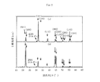
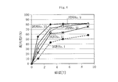
- FIG. 1 is a cross-sectional view showing an embodiment of a multilayer piezoelectric actuator as a piezoelectric ceramic electronic component according to the present invention. It is the figure which showed an example of the measurement result of a X-ray diffraction spectrum, (a) is the same composition as the sample number 9, Comprising: The figure which showed the X-ray diffraction spectrum of the non-orientated sample, (b) is the sample number 9 It is the figure which showed X-ray diffraction spectrum of. It is a figure which shows the relationship between the various rare earth elements which used the magnetic field in Example 1 as a parameter, and orientation. It is a figure which shows the relationship between the magnetic field about each sample of Example 3, and orientation degree. It is a mapping image which shows the EBSD analysis result of the sample number 31. It is a mapping image which shows the EBSD analysis result of the non-oriented sample which has the same component composition as the sample number 31, and did not apply a magnetic field.
- the ceramic sintered body according to the present invention contains a perovskite type compound represented by the general formula A m BO 3 as a main component.
- the ceramic sintered body contains 0.6 wt% or more of the first subcomponent containing at least one element of Nb and Sb, and is made of Ce, Tb, Dy, Ho, and Er.
- the second subcomponent containing at least one element selected from the inside is contained in an amount of 0.05 wt% or more, and specific crystal planes of the crystal grains are oriented in a predetermined direction.
- the specific crystal plane refers to a plane whose normal is the direction of easy magnetization of crystal grains, and in the present embodiment, it means any one of (100), (010), and (001). As described later, ⁇ 100 ⁇ plane is used.
- the predetermined direction refers to the magnetic field application direction.
- the ceramic sintered body in which the magnetic field application direction is unknown, the ceramic sintered body is cut in an appropriate cross section, and pole figure measurement by X-ray diffraction method (XRD) or crystal particle orientation by electron beam backscatter diffraction method
- XRD X-ray diffraction method
- crystal particle orientation by electron beam backscatter diffraction method By analyzing the distribution in the crystal orientation direction by analysis and fitting the distribution with a Gaussian distribution or the like, the center direction of the distribution can be set as a predetermined direction.
- a perovskite compound having a small crystal magnetic anisotropy is used. Even in such a case, a ceramic sintered body having high orientation can be obtained by applying a weak magnetic field of about 3T, and a piezoelectric ceramic electronic component having good piezoelectric characteristics having a large electromechanical coupling coefficient can be obtained at low cost. it can.
- the main component is not particularly limited as long as it is a perovskite type compound, but in the present embodiment, a PZT system or a PT system having good piezoelectric characteristics is preferred although the magnetocrystalline anisotropy is small. Can be used.
- Nb and / or Sb as the first subcomponent in the ceramic sintered body together with the second subcomponent, high orientation is imparted even when a weak magnetic field of about 3 T is applied. can do.
- Nb and Sb have the effect of increasing the crystal magnetic anisotropy of the perovskite type compound.
- Nb and Sb have an ionic radius close to that of Ti or Zr. For this reason, when an Nb compound or an Sb compound is added to the main component, these elements act as donors in the synthesis process, and a part of Ti and Zr is substituted to form a solid solution at the B site. Nb and Sb form an oxygen octahedral structure and strongly bond with oxygen ions surrounding Ti ions and Zr ions.
- the total content of Nb and / or Sb as the first subcomponent is required to be at least 0.06 wt% or more in total.
- the content of the first subcomponent is too small, and even if the second subcomponent is contained, it is sufficient for a specific crystal plane of the crystal grain. It is not possible to impart a proper orientation.
- the upper limit of the content of the first subcomponent is not particularly limited, but considering piezoelectricity, sinterability and the like, Nb is 25 wt% or less, and Sb is 4.5 wt% or less. preferable.
- the rare earth element when the rare earth element is dissolved in the A site, the rare earth element strengthens the interaction of the magnetic moments between nearby unit lattices, so the magnetic moments of the ions existing at the B site are uniform even in a weak magnetic field of about 3T. As a result, sufficient orientation can be imparted to the crystal grains even in a weak magnetic field of about 3T.
- rare earth elements it is preferable to use Ce, Tb, Dy, Ho, Er.
- Other rare earth elements for example, rare earth elements such as La, Pr, Nd, Eu, Gd, Tm, Yb, and Lu, have a smaller magnetic moment of ions than the magnetic moment of ions of Tb, Dy, Ho, and Er. . Therefore, it is considered that these rare earth elements having a small magnetic moment lack a function of strengthening the interaction of magnetic moments between adjacent unit lattices. Therefore, in order to obtain a desired orientation, a strong magnetic field of about 5 to 9 T is required. It is necessary to apply.
- Ce ions described above have an effect of effectively strengthening the interaction of magnetic moments between adjacent unit lattices, although the magnetic moment is smaller than those of Pr, Nd, Eu, Gd, or Tm. Since it contributes to the provision of orientation, it is suitable for use as the second subcomponent.
- Ce, Tb, Dy, Ho, and Er have a large magnetic moment and / or can effectively enhance the interaction of magnetic moments between adjacent unit lattices. It is possible to impart sufficient orientation.
- Ce, Tb, Dy, Ho, Er are used as the second subcomponent among the rare earth elements.
- the content of the second subcomponent is required to be at least 0.05 wt%.
- the content of the second subcomponent is less than 0.05 wt%, even if the first subcomponent is contained, it is difficult to align the magnetic moment in a weak magnetic field of about 3 T, and the crystal grains are not aligned with a specific crystal plane. Sufficient orientation cannot be imparted.
- the upper limit of the content of the second subcomponent is not particularly limited, but is preferably about 3.5 to 4.5 wt% from the viewpoint of piezoelectricity, sinterability, heat resistance, and the like. .
- orientation of crystal grains can be evaluated by, for example, the Lotgering method using an X-ray diffraction spectrum.
- the degree of orientation F can be expressed by Equation (1).
- ⁇ I (HKL) is the sum of X-ray peak intensities of a specific crystal plane (HKL) of the oriented sample
- ⁇ I (hkl) is the X-ray peak intensities of all crystal planes (hkl) of the oriented sample. It is the sum.
- ⁇ I 0 (HKL) is the sum of X-ray peak intensities of a specific crystal plane (HKL) of a reference sample, for example, a non-oriented sample
- ⁇ I 0 (hkl) is the total crystal plane (hkl) of the reference sample. Is the sum of the X-ray peak intensities.
- the X-ray peak intensity at each crystal plane can be calculated from the X-ray diffraction spectrum, and the degree of orientation F can be obtained based on Equation (1).
- a ceramic sintered body having the orientation degree F of 0.5 or more is obtained by applying a magnetic field of about 3T.
- the notation ⁇ 100 ⁇ plane does not indicate only the (100) plane, but includes the (010) plane and the (001) plane in addition to the (100) plane.
- a magnetic field is applied at the stage of the ceramic molded body, and even if the (100) plane, (010) plane, or (001) plane of crystal grains are oriented in a predetermined direction, the temperature rises during the firing process.
- the crystal system changes from the tetragonal system to the cubic system, the (100) plane, (010) plane, and (001) plane are not distinguished.
- the crystal plane facing in a predetermined direction is randomly determined as one of the (100) plane, (010) plane, and (001) plane.
- the specific crystal plane used for the ⁇ 100 ⁇ plane is randomly determined as one of the (100) plane, (010) plane, and (001) plane.
- the ceramic sintered body When measuring the X-ray diffraction spectrum using an XRD apparatus, if the area on the X-ray irradiation surface is small, the ceramic sintered body is further cut in a plane parallel to the cut surface, and the cut surface is the surface.
- the ceramic sintered bodies may be arranged so that the observation area is substantially expanded. Moreover, you may observe using the micro X-ray apparatus which can narrow down and observe the area irradiated with X-rays to a small spot. However, if the spot is extremely small and the number of ceramic particles contained in the X-ray irradiation range is extremely small, the possibility that the ceramic particles are accidentally oriented in the orientation direction cannot be denied.
- the diameter is preferably 10 times or more the average particle size of the ceramic particles.
- the crystal structure of the ceramic sintered body is a perovskite type structure. That is, the ceramic sintered body is ground into a powder, the powder is analyzed by XRD, and the obtained XRD chart is compared with a Powder Diffraction File (PDF).
- PDF Powder Diffraction File
- the crystal orientation of the crystal particles can be analyzed by using an EBSD (Electron Back Scattering Diffraction) method.
- a ceramic sintered body is cut by a suitable cross section and polished, and an electron beam narrowly focused on the cut surface is irradiated from an oblique direction, thereby diffracting the electron beam scattered backward.
- Get the pattern Kikuchi pattern the pattern Kikuchi pattern.
- SEM scanning electron microscope
- the abundance ratio of the crystal grains in which the ⁇ 100 ⁇ planes of the crystal grains are oriented in a predetermined direction within a range of 20 ° or less with respect to the magnetic field application direction is a cross-sectional area ratio of 50. It can be seen that the ⁇ 100 ⁇ plane of each crystal grain is concentrated and distributed in the magnetic field application direction. Hereinafter, in such a case, it is defined that the crystal grains are ⁇ 100 ⁇ oriented.
- a ceramic raw material a plurality of raw materials containing elements constituting the main component, for example, a Pb compound, a Ti compound, a Zr compound, etc. are prepared if the main component is PZT. Furthermore, as the ceramic raw material, a compound containing a first subcomponent containing Nb and / or Sb and a compound containing a second subcomponent containing Ce, Tb, Dy, Ho and / or Er are prepared.
- each ceramic raw material may be a simple substance or any compound such as an oxide, carbonate or hydroxide. Moreover, these mixtures may be sufficient and it does not specifically limit.
- the ceramic raw material is weighed so that the content of the first subcomponent is 0.05 wt% or more and the content of the second subcomponent is 0.6 wt% or more after firing. To do.
- these weighed ceramic raw materials are put into a ball mill containing a grinding medium such as PSZ (partially stabilized zirconia) balls, and sufficiently wet-stirred in a solvent such as pure water to obtain a mixture.
- a grinding medium such as PSZ (partially stabilized zirconia) balls
- the ceramic raw material powder thus obtained is wet mixed in a ball mill using an organic binder and a dispersant and pure water or the like as a solvent to produce a ceramic slurry.
- a normal conducting magnet or a superconducting electromagnet having a bore is used, and a forming process is performed while applying a magnetic field of 9T or less, preferably 3 to 5T in a magnetic field, thereby obtaining a ceramic compact.
- a hollow electromagnet having a bore formed with the conveying direction of the ceramic slurry as an axial direction is arranged to apply a magnetic field in the in-plane direction of the ceramic slurry, and the ceramic slurry is formed into a bore (hollow part).
- the alignment treatment can be performed while passing through.
- the magnetic field lines can be wide in the axial direction of the electromagnet, and the magnetic field application region can be widened.
- a magnetic field can be applied to the ceramic slurry for a relatively long time.
- the thickness of the ceramic molded body is preferably about 12 to 100 ⁇ m. Further, the average particle diameter of the crystal particles constituting the ceramic molded body is 0.5 to 0.5 when a wide field of view including 100 or more crystal particles in one field of view is observed with a scanning electron microscope (SEM). About 5.0 ⁇ m is preferable.
- the average particle size can be defined as follows. That is, using a SEM, the polished surface of the cross section of the ceramic molded body is observed at a magnification that includes 100 or more crystal particles within one field of view and each particle is visible. For each crystal grain to be observed, the maximum value of the width in the direction in which the width is maximum is the major axis diameter, the maximum value in the direction orthogonal to the direction in which the width is maximum is the diagonal length, and the major axis The average of the diameter and the diagonal length is defined as the particle diameter. The particle diameter of each particle thus obtained is calculated for the particles observed in the field of view, and the average of these can be defined as the average particle diameter.
- the grain boundary of the polished surface may be chemically etched using an acid or the like.
- the boundary may be clarified by heat treatment.
- this ceramic molded body is fired to produce a ceramic sintered body.
- the contents of the first subcomponent and the second subcomponent in the weighing step are 0.05 wt% or more and 0.6 wt% or more, respectively, after firing.
- the magnetic field applied to the ceramic slurry is 9 T or less (preferably 3 to 5 T). Therefore, even if a strong magnetic field of 10 T or more is not applied as in the prior art, sufficient orientation can be imparted with a weak magnetic field, and a ceramic sintered body having good orientation can be obtained at low cost. Become.
- the crystal particles are ⁇ 100 ⁇ oriented, and the degree of orientation F by the Lotgering method is 0.5 or more.
- a ceramic sintered body to which a significantly higher orientation is imparted can be obtained.
- a superconducting electromagnet that generates a magnetic field of 3 to 5 T can have a larger bore diameter than a superconducting electromagnet that generates a strong magnetic field of 9 T or more. Therefore, when a magnetic field of 3 to 5 T is applied, crystal grains can be oriented using a superconducting electromagnet with a large bore diameter, which greatly improves productivity and reduces the cost of desired ceramic sintering. The body can be manufactured easily.
- the main component contains the first and second subcomponents, but at least one element selected from Ni, Co, Fe, Mn, Mg, and Zn is used as the third component.
- Inclusion as a subcomponent is preferable for further improving the orientation, and inclusion of such a third subcomponent makes it possible to obtain a larger electromechanical coupling coefficient.
- Ni, Co, Fe, Mn, Mg, and Zn as the third subcomponent are similar to the first subcomponent Nb and Sb in terms of the elements existing at the B site such as Ti and Zr and the ion radius. Nearly, it dissolves in the B site as an acceptor.
- These third subcomponents have a large magnetic moment or an effect of increasing the magnetocrystalline anisotropy, which contributes to improving the orientation.
- the first subcomponent that acts as an acceptor is added to the first subcomponent. It is possible to facilitate the solid solution of the subcomponent of B to the B site, thereby further improving the orientation.
- the total amount of the subcomponent is 5 mol parts with respect to 100 mol parts of the main component. Even if it does above, deterioration of an electrical property does not occur, but since the responsiveness with respect to a magnetic field increases, the ceramic sintered compact to which the desired big orientation was provided with the magnetic field of 3-5T can be obtained easily.
- Pb, Ti, and Zr measured by the composition analysis form Pb a (Ti, Zr) b O c .
- the content of each element thus measured is divided by the atomic weight of each element and converted to a molar amount.
- the molar amount of Pb is compared with the sum of the molar amounts of Ti and Zr, the larger one is regarded as the molar amount of the main component, and the molar amount of each element is set so that the molar amount of the main component is 100 mol parts. The amount is normalized and this is defined as 100 mole parts of the main component.
- the total mole part of the subcomponents with respect to 100 mole parts of the main component is defined as follows. First, the molar amounts of elements other than Pb, Ti, and Zr are summed, and the molar amount is normalized by the same method as described above. Next, the molar amount of elements other than the standardized Pb, Ti, and Zr is divided by 100 mole parts of the main component, and this is multiplied by 100, and this is the total mole portion of subcomponents relative to 100 mole parts of the main component. Define.
- the composition of the ceramic sintered body is, for example, the XRF method (X-ray fluorescence analysis) and the ICP-AES method (Inductively Coupled Plasma-Atomic Emission Spectroscopy). Can be obtained by using together.
- XRF method X-ray fluorescence analysis
- ICP-AES method Inductively Coupled Plasma-Atomic Emission Spectroscopy
- the XRF method detects the fluorescent X-rays that are excited by the irradiation of primary X-rays, and qualifies and quantifies the elements. That is, by using the XRF method, it is possible to specify the element type from the detected fluorescent X-ray wavelength or the amount of the element from the intensity of the fluorescent X-ray wavelength.
- the XRF method since the X-ray intensity of the detected fluorescent X-ray slightly changes depending on the particle size, surface state, etc. of the ceramic sintered body, the content of the constituent elements of the ceramic sintered body is highly accurate. It is difficult to measure. Further, since the XRF method is a surface analysis, it is not suitable for the case where it is assumed that a gradient distribution or segregation of the composition exists between the surface and the inside, such as a ceramic sintered body. For this reason, first, the XRF method is used to identify the element type contained in the ceramic sintered body and measure the approximate content. Next, the ceramic powder obtained by pulverizing the ceramic sintered body is dissolved in nitric acid to form a solution, and the content of the element is determined using the ICP-AES method.
- the ceramic powder is made into a solution and the composition in the solution sample is analyzed. Therefore, an element that does not cause quantitative fluctuation in the solution process can be quantitatively analyzed.
- the amount of gaseous oxygen cannot be quantified. Therefore, although it is necessary to confirm that the oxygen component is contained in the ceramic sintered body, this can be confirmed by the following method.
- EDX Electronic dispersive X-ray spectroscopy
- WDX Widelength dispersive X-ray spectroscopy
- XRD method X- There is a method of checking the crystal structure by using a ray (Diffraction: X-ray diffraction) method and confirming that it is an oxide crystal structure.
- the ceramic sintered body is heated in an oxygen atmosphere to check whether or not gas is generated, and by checking the generated gas species, it is confirmed whether or not the sintered body before heating is an oxide. can do. If the ceramic sintered body can be confirmed to be an oxide by these methods, it can be considered that the components other than the element species determined by the XRF method and the ICP-AES method are oxygen.
- the piezoelectric ceramic electronic component is a laminated type having an internal electrode as will be described later
- the internal electrode component may be eluted in the process of making the sample into solution. Therefore, if the piezoelectric ceramic body, which is a ceramic sintered body, is dissolved as it is to form a solution, the content of the metal element in the piezoelectric ceramic cannot be determined. For this reason, it is preferable to measure by the ICP-AES method after peeling or polishing and removing the internal electrode.
- each content of the first component, the second component, and the third component described above is set such that the weight of the ceramic sintered body immediately before being converted into a solution for analysis is 100 wt%, and the content of each element relative to the weight is 100 wt%.
- the value is obtained as the atomic weight ratio.
- the polished surface may be quantitatively analyzed by the EDX method or the WDX method, and the element content may be obtained by comparing with a quantitative analysis value of a ceramic whose composition is known.
- the contents of the first component, the second component, and the third component are such that the weight of the ceramic sintered body at the analysis stage is 100 wt%, and the weight ratio of the atoms of each element to that The value obtained as
- FIG. 1 is a cross-sectional view showing an embodiment of a multilayer piezoelectric actuator as a piezoelectric ceramic electronic component according to the present invention.
- the multilayer piezoelectric actuator includes a piezoelectric ceramic body 1 and piezoelectric ceramic body 1. External electrodes 2a and 2b made of a conductive material such as Ag or Ni are provided at both ends.
- the piezoelectric ceramic body 1 is formed by alternately laminating piezoelectric ceramic layers made of the ceramic sintered body of the present invention and internal electrodes 3a to 3g formed of a conductive material mainly composed of Ag, Pd, Pt, or the like. It is tied.
- one end of the internal electrodes 3a, 3c, 3e, and 3g is electrically connected to one external electrode 2a, and one end of the internal electrodes 3b, 3d, and 3f is electrically connected to the other external electrode 2b.
- the laminated piezoelectric actuator when a voltage is applied between the external electrode 2a and the external electrode 2b, the laminated piezoelectric actuator is displaced in the laminating direction indicated by the arrow X due to the piezoelectric longitudinal effect, and is laminated as indicated by the arrow Y due to the piezoelectric lateral effect. Displacement in the direction perpendicular to the direction.
- a ceramic raw material powder is produced by the same method and procedure as described above.
- the ceramic raw material powder obtained in this way is crushed, and then an organic binder and a dispersant are added and wet-mixed in a ball mill using pure water as a solvent to obtain a ceramic slurry. Thereafter, a forming process is performed using a doctor blade method or the like while applying a magnetic field of 3 to 9 T, thereby producing a ceramic green sheet.
- a conductive layer for a predetermined shape is formed on the ceramic green sheet by screen printing using a conductive paste for internal electrodes mainly composed of Ag, Pd, Pt or the like.
- the ceramic green sheets on which these conductive layers are formed are sandwiched and pressure-bonded.
- a ceramic laminate in which conductive layers and ceramic green sheets are alternately laminated is produced.
- the ceramic laminate is cut into a predetermined size and accommodated in an alumina pod (sheath), subjected to a binder removal treatment at a predetermined temperature (for example, 250 to 500 ° C.), and then in a predetermined atmosphere (for example, Firing in a reducing atmosphere) and a predetermined temperature (for example, 1000 to 1200 ° C.) to form the piezoelectric ceramic body 1 in which the internal electrodes are embedded.
- a predetermined temperature for example, 250 to 500 ° C.
- a predetermined atmosphere for example, Firing in a reducing atmosphere
- a predetermined temperature for example, 1000 to 1200 ° C.
- a conductive paste for an external electrode made of Ni—Cu alloy, Ag, or the like is applied to both main surfaces of the piezoelectric ceramic body 1 and subjected to a baking process at a predetermined temperature (for example, 750 ° C. to 850 ° C.). 2a and 2b are formed.
- polarization treatment is performed by applying a predetermined electric field for a predetermined time in an insulating oil such as silicon oil heated to a predetermined temperature (for example, 80 ° C.), whereby a laminated piezoelectric actuator is manufactured.
- the external electrodes 2a and 2b may be formed by a thin film forming method such as a sputtering method or a vacuum evaporation method as long as the adhesion is good.
- the laminated piezoelectric actuator has a high orientation because the piezoelectric ceramic layer is formed of the ceramic sintered body. Therefore, the laminated piezoelectric actuator has a large electromechanical coupling coefficient and a good electrical characteristic compared to the conventional one. A piezoelectric actuator can be obtained.
- the ceramic sintered body may contain a trace amount of inevitable impurities such as Hf, Ca, Al, and Si in the manufacturing process, but it does not affect the orientation and piezoelectric characteristics.
- the multilayer piezoelectric actuator described above is an example, and it goes without saying that the piezoelectric ceramic electronic component can be widely applied to a single plate type piezoelectric component and other piezoelectric components using piezoelectricity other than the multilayer piezoelectric actuator.
- Pb 3 O 4 , TiO 2 , ZrO 2 , Nb 2 O 5 containing Nb (first subcomponent), NiO containing Ni (third subcomponent) are prepared, Furthermore, La 2 O 3 , CeO 2 , Pr 6 O 11 , Nd 2 O 3 , Eu 2 O 3 , Gd 2 O 3 , Tb 2 O 3 , Dy 2 O 3 , Ho 2 O 3 as rare earth oxides, Er 2 O 3 , Tm 2 O 3 , Yb 2 O 3 , and Lu 2 O 3 were prepared.
- these ceramic raw materials are weighed so that the element content after sintering is as shown in Table 1, and such a weighed product is put into a ball mill together with pure water as a solvent and PSZ balls as a grinding medium, Mix and stir for 15 hours in a ball mill.
- this mixture was dried, calcined at a temperature of 1000 ° C., and then dry-pulverized to obtain a ceramic raw material powder (composite).
- these ceramic slurries were subjected to a forming process while applying a magnetic field of 1 to 9 T, thereby producing a ceramic formed body.
- this ceramic molded body was fired in an oxygen atmosphere at a maximum firing temperature of 1100 ° C. for 3 hours to produce samples Nos. 1 to 14 (ceramic sintered bodies).
- the element contained in the sample was identified using the XRF method, and the approximate content was measured.
- each sample was pulverized in a mortar, and the obtained powder was dissolved in nitric acid to form a solution, and the content of the element contained in the solution sample was determined using the ICP-AES method.
- FIG. 2 is a diagram showing an example of the measurement result of the X-ray diffraction spectrum, and shows the case of sample number 9.
- FIG. 2A is an X-ray diffraction spectrum of a non-oriented sample to which no magnetic field is applied
- FIG. 2B is an X-ray diffraction spectrum when a 3T magnetic field is applied.
- the horizontal axis represents the diffraction angle 2 ⁇ (°)
- the vertical axis represents the X-ray intensity (a.u.).
- X-ray peak intensities of the (001) plane and (100) plane appear when the diffraction angle 2 ⁇ is 21 to 23 °, and (101) when the diffraction angle 2 ⁇ is 30 to 32 °.
- the X-ray peak intensity of the (110) plane appears, and the X-ray peak intensity of the (111) plane appears when the diffraction angle 2 ⁇ is 38 to 39 °.
- these X-ray peak intensities were set to I (001), I (100), I (101), I (110), and I (111) in order.
- the X-ray peak intensities are sequentially set to I 0 (001), I 0 (100), I 0 (101), I 0 (110), I 0 ( 111).
- Table 1 shows the content (wt%) of the elements detected by the ICP-AES method and the degree of orientation F of each sample Nos. 1 to 14. As described above, since each sample was confirmed to have an oxide structure, it was assumed that the contained component other than the elements detected by the ICP-AES method was oxygen. The degree of orientation F is shown in terms of “%”.
- Sample Nos. 2, 4 to 7, and 12 to 14 contain La, Pr, Nd, Eu, Gd, Tm, Yb, Lu and rare earth elements outside the scope of the present invention as the second subcomponent.
- the content was 0.05 wt% or more, but even when a 3T magnetic field was applied, the degree of orientation F was 19 to 49% and less than 50%, indicating that the crystal orientation was poor.
- Sample Nos. 3 and 8 to 11 contain Ce, Tb, Dy, Ho, and Er within the range of the present invention in the range of 1.31 to 1.58 wt%. That is, since the rare earth element within the range of the present invention is contained in an amount of 0.05 wt% or more, the orientation degree F is 58 to 82% when a magnetic field of 3 T is applied, and it has been found that the film has good orientation.
- FIG. 3 shows the relationship between the rare earth elements and the degree of orientation.
- the horizontal axis represents the element type of the rare earth element, and the vertical axis represents the orientation degree F (%).
- a case is shown in which magnetic fields of 1T for ⁇ , 3T for ⁇ , 5T for ⁇ , and 9T for ⁇ are applied.
- Ce, Tb, Dy, Ho, and Er within the scope of the present invention have a good degree of orientation F, and an extremely large degree of orientation F of 74 to 82% is obtained when a 9T magnetic field is applied. It has gained.
- Dy and Tb have an orientation degree F of 50% or more even when the applied magnetic field is 1 T, and it was found that they are more preferable.
- La, Pr, Nd, Eu, Gd, Tm, Yb, and Lu outside the scope of the present invention are inferior in orientation.
- samples Nos. 21 to 26 were prepared by the same method and procedure as in Example 1, and subjected to composition analysis, and the degree of orientation was obtained.
- Table 2 shows the element content (wt%) and the orientation degree F of each sample Nos. 21 to 26.
- Example 1 the components other than the elements detected by the ICP-AES method are regarded as oxygen, and the orientation degree F is converted to “%”.
- Sample Nos. 21 and 25 have low Nb contents of 0.036 wt% and 0.041 wt% and do not contain the second subcomponent, so that the applied magnetic field is not oriented at 1 T, and a 3 T magnetic field is applied. Even when applied, the degree of orientation F was 17% and 8%, indicating that the crystal orientation was extremely inferior.
- the content of Dy as the second subcomponent is 1.54 wt%, but the content of Nb is as small as 0.041 wt%, so the degree of orientation is not limited even when a magnetic field of 3 to 9 T is applied. F was 24 to 30%, and it was found that the crystal orientation was inferior.
- the Nb contents are 0.613 wt% and 0.6 wt% or more, but the second subcomponent is not contained, so the orientation degree F does not increase even when a magnetic field of 3 to 5 T is applied. It was 12 to 30%, and it was found that the crystal orientation was inferior.
- Sample No. 24 has a Nb content of 0.628 wt%
- Sample No. 26 has a total content of Nb and Sb of 0.756 wt%, both containing 0.6 wt% or more.
- the Dy content is 1.50 wt% for sample number 24 and 1.44 wt% for sample number 26, both of which are 0.05 wt% or more, so even when a 3T magnetic field is applied, The degree was 56 to 63%, and it was found that good orientation was imparted.
- the content of the first subcomponent (Nb, Sb) needs to be 0.6 wt% or more, but even if only the first subcomponent is contained, the desired orientation cannot be imparted, It has been found that by including both the first subcomponent and the second subcomponent, good orientation can be imparted by these synergistic effects.
- sample number 24 containing Ni as the third subcomponent could increase the degree of orientation F compared to the sample number 26 not containing Ni. That is, it has been found that the orientation can be further improved by containing the third subcomponent.
- samples Nos. 31 to 33 were prepared by the same method and procedure as in Example 1, subjected to composition analysis, and the degree of orientation was determined.
- Table 3 shows the element content (wt%) and the degree of orientation F of each sample Nos. 31 to 33.
- Sample No. 1 not containing Dy and Sample No. 9 having a Dy content of 1.50 wt% are shown again.
- Example 1 the components other than the elements detected by the ICP-AES method are regarded as oxygen, and the orientation degree F is converted to “%”.
- Sample Nos. 31 to 33 have a Dy content of 0.05 to 0.50 wt%, and all have a degree of orientation of 62 to 72% when a 3T magnetic field is applied. I understood.
- the second subcomponent such as Dy is contained in an amount of 0.05 wt% or more, a ceramic sintered body imparted with a high orientation in combination with the effect of adding a predetermined amount of the first subcomponent. It turns out that it is obtained.
- FIG. 4 is a diagram showing the relationship between the magnitude of the applied magnetic field and the degree of orientation.
- the horizontal axis represents the magnetic field (T), and the vertical axis represents the orientation degree F (%).
- the ⁇ mark indicates the sample number 1
- the x mark indicates the sample number 31
- the ⁇ mark indicates the sample number 32
- the ⁇ mark indicates the sample number 33
- the ⁇ mark indicates the sample number 9.
- Sample No. 31 was cut and its cross section was polished, and an electron beam narrowly focused on this cut surface was irradiated from an oblique direction, and an electron beam Kikuchi pattern was obtained by backward scattering. And this Kikuchi pattern was analyzed and the crystal orientation of the location where the electron beam collided with the sample was specified. This was observed with a SEM over a wide range including a large number of crystal grains of 100 to 1000, analyzed using the EBSD method, and the crystal orientation distribution state of each crystal grain was examined.
- FIG. 5 is a mapping diagram showing a distribution state of ⁇ 100 ⁇ orientation included in a range of 20 ° or less with respect to the application direction of the magnetic field for Sample No. 31.
- FIG. 6 is a mapping diagram showing the analysis result, and shows a distribution state of ⁇ 100 ⁇ orientation included in a range of 20 ° or less with respect to the magnetic field application direction for the non-oriented sample.
- crystal grains are shown in white, gray, and black shading, and a crystal in which the portion from black to gray is ⁇ 100 ⁇ oriented within a range of 20 ° or less with respect to the magnetic field application direction. Shows particles.
- sample No. 31 has a large number of crystal particles displayed in black to gray and the presence of ⁇ 100 ⁇ oriented crystal particles included in a range within 20 ° with respect to the direction of application of the magnetic field.
- the ratio was 57.4% in terms of the cross-sectional area ratio, and it was confirmed that Sample No. 31 was ⁇ 100 ⁇ oriented.
- the characteristics were evaluated by varying the element type and content of the third subcomponent.
- Pb 3 O 4 , TiO 2 , ZrO 2 , Nb 2 O 5 containing Nb, Sb 2 O 3 containing Sb, and Dy 2 O 3 containing Dy were prepared as ceramic raw materials.
- NiO, CoO, Fe 2 O 3 , MnO 2 , MgO, and ZnO containing the subcomponents were prepared.
- the molar content of the subcomponent with respect to 100 mol parts of the main component and the molar ratio of the third subcomponent with respect to the first subcomponent were calculated based on the results of the composition analysis.
- the molar amount of each element was calculated by dividing the content of each element obtained by composition analysis by the respective atomic weight.
- the total amount of the molar amount of Ti element and the molar amount of Zr element was compared with the molar amount of Pb element, and the larger one was defined as the molar amount of the main component.
- the sum of the molar amount of elements other than the main component elements (Pb, Ti, Zr) is divided by the molar amount of the main component, multiplied by 100, and the molar content of subcomponents relative to 100 mol parts of the main component was calculated.
- the molar amount of the third subcomponent was divided by the molar amount of the first subcomponent to calculate the molar ratio of the third subcomponent to the first subcomponent.
- Table 4 shows the element content of each sample of sample numbers 41 to 55
- Table 5 shows the molar ratio of the third subcomponent and the first subcomponent of each sample of sample numbers 41 to 55, the main component 100.
- the total amount of subcomponents (mole part) and the degree of orientation F relative to the mole part are shown.
- the components other than the elements detected by the ICP-AES method are regarded as oxygen, and the degree of orientation F is converted to “%”.
- the Nb content is 0.594 wt% and 0.6 wt% or less
- the Ni content is 0.185 wt% and 0.29 wt% or less
- the second subcomponent is Since it was not contained, the applied magnetic field was not oriented at 1T, and even when a 3T magnetic field was applied, the orientation degree F was 17%, indicating that the crystal orientation was poor.
- the Dy content is 0.15 wt% and 0.05 wt% or more, but the Nb content is 0.591 wt% and 0.6 wt% or less, and the Ni content is also 0.161 wt%. Therefore, even when a magnetic field of 3 to 9 T was applied, the degree of orientation F was as low as 24 to 30%, indicating that the crystal orientation was inferior.
- Sample No. 44 has Nb contents of 0.613 wt% and 0.6 wt% or more, but does not contain the second subcomponent, and the content of Co as the third subcomponent is also 0. Therefore, in order to obtain an orientation degree of 50% or more, it was necessary to apply a 9T magnetic field. With an applied magnetic field of 3 to 5T, only an orientation degree F of less than 50% was obtained.
- the Nb content is 2.88 wt% and 0.6 wt% or more
- the Fe content as the third subcomponent is 0.86 wt% and 0.29 wt% or more.
- Sample No. 48 has Nb contents of 2.95 wt% and 0.6 wt% or more, and the content of Mn as the third subcomponent is 0.86 wt% and 0.29 wt% or more. 2 was not contained, so that it was not oriented when a magnetic field of 5 T or less was applied, and even when a strong magnetic field of 9 T was applied, the degree of orientation F was 2%, indicating that the orientation was significantly inferior. .
- Sample No. 50 has Nb contents of 2.96 wt% and 0.6 wt% or more, and Mg content as the third subcomponent is 0.86 wt% and 0.29 wt% or more. 2 subcomponents are not contained, and therefore, when the applied magnetic field is 3T or less, the orientation degree F is 40% or less, and in order to obtain the orientation degree F of 50% or more, it is necessary to apply a magnetic field of 5T or more. I found out.
- Sample No. 52 has Nb contents of 2.88 wt% and 0.6 wt% or more, and Zn content as the third subcomponent is also 1.00 wt% and 0.29 wt% or more. 2 is not contained, and therefore when the applied magnetic field is 5T or less, the orientation degree F is less than 50%, and in order to obtain the orientation degree F of 50% or more, it is necessary to apply a magnetic field of 9T or more. I understood that.
- the total content of Nb and Sb as the first subcomponent is 3.858 wt% and 0.6 wt% or more, and the content of Ni as the third subcomponent is also 0.916 wt%. 0.29 wt% or more, but the second subcomponent is not contained. Therefore, when the applied magnetic field is 5 T or less, the orientation degree F is less than 50%, and an orientation degree F of 50% or more is obtained. It was found that it was necessary to apply a strong magnetic field of 9 T or more.
- Sample Nos. 43, 45, 47, 49, 51, 53, and 55 have a content of the first subcomponent of 0.994 to 3.745 wt%, 0.6 wt% or more, and contain Dy.
- the amount is 0.15 to 1.54 wt%, which is 0.15 wt% or more, and the content of the third subcomponent (Ni, Co, Fe, Mn, Mg, Zn) is 0.29 wt% or more in the present invention.
- the degree of orientation F was as high as 50% or more with an applied magnetic field of 3T.
- Sample Nos. 45 and 51 can obtain a high orientation having an orientation degree F of 57 to 63% even when a weak magnetic field of 1T is applied.
- Sample numbers 43, 45, 47, 49, 51, 53, and 55 described above have a molar ratio of the third subcomponent to the first subcomponent of 0.45 to 0.54. It was found that good orientation could be obtained even when the component contained 5 mol parts or more of subcomponents with respect to 100 mol parts of the main component.
- Example 3 Using the sample number 9 of Example 1 and the sample number 32 of Example 3, a piezoelectric ceramic electronic component was produced.
- an electromechanical coupling factor k 31 was measured using a resonance-antiresonance method using an impedance analyzer (manufactured by Agilent Technologies, 4294A).
- Table 6 shows the electromechanical coupling coefficient k 31 of sample numbers 9 and 32 together with the non-oriented samples (9 ′, 32 ′).
- the increase factor is for a non-oriented sample.
- Sample numbers 9 ′ and 32 ′ which are non-oriented samples, had electromechanical coupling coefficients k 31 of 25.5% and 32.2%, respectively.
- Sample Nos. 9 and 32 to which a 3T magnetic field was applied had high orientation degrees F of 87% and 67%, respectively, so that the electromechanical coupling coefficient k 31 was 29.2% and 36.4%.
- the increasing magnifications were 1.15 times and 1.13 times, respectively.
- a ceramic sintered body having sufficient crystal orientation can be obtained even when a weak magnetic field is applied compared to the prior art, and a piezoelectric ceramic having a better electromechanical coupling coefficient can be obtained by using this ceramic sintered body.
- An electronic component can be obtained.
Landscapes
- Engineering & Computer Science (AREA)
- Chemical & Material Sciences (AREA)
- Ceramic Engineering (AREA)
- Manufacturing & Machinery (AREA)
- Mechanical Engineering (AREA)
- Composite Materials (AREA)
- Materials Engineering (AREA)
- Structural Engineering (AREA)
- Organic Chemistry (AREA)
- Compositions Of Oxide Ceramics (AREA)
Abstract
圧電セラミックは、主成分が、PZT等のペロブスカイト型化合物で形成されている。Nb及び/又はSbが0.6wt%以上含有され、Ce、Tb、Dy、Ho、及び/又はErが、0.05wt%以上含有されている。Ni、Fe、Co、Mn、Mg、及び/又はZnを0.29wt%以上含有するのも好ましい。結晶粒子の結晶軸は、{100}配向し、3Tの磁場印加で、ロットゲーリング法による配向度が0.5以上の配向性を有する。この圧電セラミックを使用してセラミック素体1を形成する。これにより弱い磁場印加でも十分な結晶配向性を有する圧電セラミックと該圧電セラミックの製造方法を実現し、この圧電セラミックを使用することにより、より良好な電気機械結合係数を得ることができる圧電セラミック電子部品を実現する。
Description
本発明はセラミック焼結体、セラミック焼結体の製造方法及び圧電セラミック電子部品に関し、より詳しくは結晶粒子の特定の結晶面を所定方向に配向させたセラミック焼結体とその製造方法、及びこのセラミック焼結体を使用した積層圧電アクチュエータ等の圧電セラミック電子部品に関する。
今日、様々な電子機器に圧電セラミック電子部品が搭載されているが、これらの圧電セラミック電子部品では、各種のセラミック材料を主成分とするセラミック焼結体が広く使用されている。
この種のセラミック焼結体では、結晶粒子の特定の結晶面の配向性を制御することにより、圧電特性等の各種特性が向上することが知られており、結晶粒子に磁場を印加することにより配向化が可能である。
磁場を形成する方法としては、従来より、永久磁石を用いる方法と電磁石を用いる方法とが知られている。
しかし、永久磁石を用いる場合、現時点で最も強い磁場が得られるネオジム磁石でも、最大となる磁石表面で数百mT程度の磁束密度しか得られない。しかも実際に結晶粒子に付与される磁場は、磁石表面からの距離の2乗~3乗に反比例するため、印加磁場は更に低くなる。したがって、永久磁石では所望の圧電特性を得る程度に結晶粒子の特定の結晶面を配向させるのは困難である。
一方、電磁石については、非磁性材料からなる中空円筒状のボア(bore)や磁性材料からなる円柱状の磁芯にCu等の導線を巻回させてコイルを形成した常伝導電磁石と、Cu等の導線に代えて超伝導線を用いた超伝導電磁石とがあり、通電される電流と巻き数を制御することにより磁束密度を高めることができ、強磁場の実現が可能である。
しかしながら、常伝導電磁石は、過剰な大電流を通電させると、ジュール熱が発生し、コイルが焼損するおそれがある。このジュール熱を冷却装置で除去する水冷式の常伝導電磁石も知られているが、一般的な常伝導電磁石では、磁束密度が1T程度の弱磁場しか得られていないのが現状である。
これに対し超伝導電磁石は、電気抵抗を有さず、ジュール熱が発生しないことから、大電流を通電することが可能であり、磁束密度が10T以上の強磁場を実現することが可能である。
そして、このような10T以上の強磁場を印加して結晶粒子を配向させた技術として、例えば特許文献1や特許文献2が知られている。
特許文献1には、多結晶セラミック粉末を含むセラミックスラリーを得る工程と、前記セラミックスラリーを磁場中で成形してセラミック成形体を得る工程と、前記セラミック成形体を焼成する工程とを有する配向性セラミックスの製造方法であって、前記多結晶セラミック粉末は、ペロブスカイト構造を有する主成分と前記主成分100モル部に対して5モル部以下(ただし、0モル部を除く。)の割合で含有される副成分とを含み、前記副成分は磁気モーメントが0ではない3d遷移金属イオンまたは磁気モーメントが0ではない希土類遷移金属イオンからなる群より選択される少なくとも1種である配向性セラミックスの製造方法が提案されている。
この特許文献1では、主成分としてBaTiO3やPb(Zr0.5Ti0.5)O3を使用し、さらに磁気モーメントが0ではない3d遷移金属イオンまたは希土類遷移金属イオンとしてMn2+,Fe3+,Ce3+,Nd3+,Sm3+及びDy3+を前記主成分に含有させ、12Tの磁場を印加することにより、ロットゲーリング法による配向度が10.4~85.4%の配向性セラミックを得ている。
特許文献1には、磁場を生成する手段については記載されていないが、磁束密度が10Tを超える強磁場を実現していることから、超伝導電磁石を使用しているものと考えられる。
また、特許文献2には、セラミックスを構成する金属元素を少なくとも含む金属酸化物粉体を分散させた第1のスラリーを基材上に設置する工程と、前記第1のスラリーに対して磁場を印加し凝固させて第1の成形体からなる下引き層を形成する工程と、前記下引き層の上に、前記セラミックスを構成する金属酸化物粉体を含む第2のスラリーを設置する工程と、前記第2のスラリーに対して磁場を印加し凝固させて第2の成形体を形成して前記第2の成形体と前記下引き層の積層体を得る工程と、前記第2の成形体と前記下引き層の積層体から前記下引き層を除去した後に焼成するか、又は前記第2の成形体と前記下引き層の積層体を焼成した後に前記下引き層を除去して、前記第2の成形体からなるセラミックスを得る工程を有するセラミックスの製造方法が提案されている。
この特許文献2では、タングステンブロンズ構造やペロブスカイト構造等の金属酸化物粉体にFe、Co、Ni、Gd、Tb、Dy、Ho、Er、Tm等の磁性金属を0.05~10wt%含有させたり、Mn酸化物を含有させ、10Tの強磁場で結晶粒子を配向させたりしている。
そして、この特許文献2では、磁場の形成手段として超伝導電磁石を使用し、ペロブスカイト構造のBaTiO3に酸化マンガンを含有させたスラリーに対し、10Tの磁場を印加し、これによりロットゲーリング法による配向度が29%のセラミックスを得ている。
しかしながら、特許文献1や特許文献2では、超伝導電磁石を使用して10T以上の強磁場を発生させ、結晶粒子を配向させているものの、以下の理由により、大きな空間に強磁場を生成するのは困難である。
すなわち、超伝導電磁石の主体となる超伝導材料には、臨界磁場が存在し、特定の磁場を超えると超伝導状態が壊れて常伝導状態に戻ってしまう。このためコイル近傍に発生する磁場の大きさには限界がある。
しかも、超伝導電磁石では、磁束密度は、通電されるコイルからの距離の2乗に反比例して低下することから、ボアの内部に発生する磁場を利用する場合は、ボアの直径が大きくなると、磁場が急速に弱くなる。
このように超伝導電磁石は、臨界磁場が存在することから磁場を強くするには限界があり、さらにボアの直径が大きくなると内部に発生する磁場が急速に弱くなる。このため市販されている超伝導電磁石は、中心磁場が10T程度の場合でボアの直径が100mm程度であり、中心磁場が15T程度の場合でボアの直径が50mm程度であり、いずれも小さく、このため超伝導電磁石を工業的な量産性が要求される用途に使用するのは困難な状況にある。
また、強磁性を有さない結晶粒子を主成分とする物質を磁場印加により配向させる場合、結晶粒子に作用する回転モーメントは印加磁場の2乗に比例する。このため磁場の大きさを弱くすると、大きな配向度を有する配向セラミックスを得るのが益々困難になる。例えば、磁場を12Tから3Tに低下させた場合、回転モーメントは1/16に低下し、したがって所望の大きな配向度を有する配向セラミックスを得るのは極めて困難になる。
さらに、特許文献2では、10Tの磁場を印加したとしても、配向度は29%しか得られていない。したがって、より大きな電気機械結合係数k31を得るためには、より大きな配向度を有するセラミック焼結体の実現が望まれる。
本発明はこのような事情に鑑みなされたものであって、弱い磁場印加でも十分な結晶配向性を有するセラミック焼結体と該セラミック焼結体の製造方法を提供することを目的とし、またこのセラミック焼結体を使用することにより、より良好な電気機械結合係数を得ることができる圧電セラミック電子部品を提供することを目的とする。
圧電体に使用されるセラミック材料としては、チタン酸鉛(以下、「PT」という。)やチタン酸ジルコン酸鉛(以下、「PZT」という。)等のペロブスカイト型結晶構造を有する複合酸化物(以下、「ペロブスカイト型化合物」という。)が広く使用されている。
そこで、本発明者らは、PZTを使用して鋭意研究を行ったところ、Nb及びSbのうちの少なくとも一方の元素を0.6wt%以上含有させ、かつ希土類元素の中からCe、Tb、Dy、Ho、及びErのうちの少なくとも1種の元素を選択して0.05wt%以上含有させることにより、3Tの弱磁場を印加しても良好な結晶配向性を有するセラミック焼結体を得ることができるという知見を得た。
PZTは結晶磁気異方性が小さく、大きな磁気モーメントを有するイオンが存在しないことから、磁場の印加による配向性の付与が困難とされている。しかしながら、上述したように配向性付与が困難とされるPZTであっても、添加元素とその含有量を工夫することにより、弱磁場の印加で格段に優れた配向性が得られることから、同様に結晶磁気異方性が小さく、大きな磁気モーメントを有さないPT等の他のペロブスカイト型化合物にも適用可能と考えられる。
本発明はこのような知見に基づきなされたものであって、本発明に係るセラミック焼結体は、一般式AmBO3で表されるペロブスカイト型結晶構造を有する複合酸化物を主成分として含み、Nb及びSbのうちの少なくとも一方の元素を含む第1の副成分が、0.6wt%以上含有されると共に、Ce、Tb、Dy、Ho、及びErの中から選択された少なくとも1種の元素を含む第2の副成分が、0.05wt%以上含有され、結晶粒子の特定の結晶面が、所定方向に配向されていることを特徴としている。
また、本発明のセラミック焼結体は、少なくとも前記第1及び前記第2の副成分を含み、Ni、Fe、Co、Mn、Mg、及びZnの中から選択された少なくとも1種の元素を含む第3の副成分が、0.29wt%以上含有されているのも好ましい。
上記第3の副成分は、大きな磁気モーメントを有し、しかもアクセプタとしてBサイトに固溶することから、ドナーとしてBサイトに固溶する第1の副成分と相俟って大きな磁気モーメント或いは大きな結晶磁気異方性を有する元素のBサイトへの固溶量を増加させることができ、これにより結晶粒子の特定の結晶面に対して更なる配向性付与が可能となる。
また、本発明のセラミック焼結体は、前記第1の副成分の含有量に対する前記第3の副成分の含有量は、モル比で0.45~0.54であるのが好ましい。
さらに、本発明のセラミック焼結体は、前記主成分以外の前記副成分の含有量総計が、主成分100モル部に対し5モル部以上とするのも好ましい。
このように第1の副成分と第3の副成分の含有割合を調整することにより、副成分の含有量総計を主成分100モル部に対し5モル部以上としても電気特性の劣化を招くことなく、従来よりも弱い磁場であっても、より大きな配向度を有するセラミック焼結体を容易に得ることができる。
また、本発明のセラミック焼結体は、前記特定の結晶面は{100}面であるのが好ましい。
さらに、本発明のセラミック焼結体は、前記特定の結晶面は{100}面であり、ロットゲーリング法による配向度が、0.5以上であるのが好ましい。
また、本発明のセラミック焼結体は、前記特定の結晶面は{100}面であり、前記結晶粒子の配向は磁場印加によってなされると共に、前記磁場印加の方向に対し20°以内の範囲で前記結晶粒子の{100}面が前記所定方向に配向している前記結晶粒子の存在比率は、断面積比で50%以上であるのが好ましい。
また、本発明のセラミック焼結体は、前記存在比率が、電子線後方散乱回折法に依拠した解析結果に基づいて算出される。
また、本発明のセラミック焼結体は、前記複合酸化物が、PZT系化合物であるのが好ましい。
また、本発明のセラミック焼結体は、1視野内に前記結晶粒子が100個以上含まれる視野の広さを走査型電子顕微鏡で観察した場合の前記結晶粒子の平均粒子径が0.5~5μmであるのが好ましい。
また、本発明に係るセラミック焼結体の製造方法は、一般式AmBO3で表されるペロブスカイト型結晶構造を有する複合酸化物を主成分として含み、複数の副成分を含むセラミック焼結体の製造方法であって、セラミック素原料として、前記主成分である元素を含有した複数の原料と、Nb及びSbのうちの少なくとも一方の元素を含む第1の副成分を含有した原料と、Ce、Tb、Dy、Ho、及びErの中から選択された少なくとも1種の元素を含む第2の副成分を含有した原料とを用意し、これらセラミック素原料を秤量する秤量工程と、前記セラミック素原料と、前記第1及び第2の副成分とを合成した合成物を作製する合成工程と、前記合成物をスラリー化し、セラミックスラリーを作製するセラミックスラリー作製工程と、前記セラミックスラリーに磁場を印加しながら成形加工を施し、セラミック成形体を作製する成形体作製工程と、前記セラミック成形体を焼成する焼成工程とを含み、前記秤量工程は、前記第1の副成分及び前記第2の副成分の各含有量が焼成後にそれぞれ0.05wt%以上、及び0.6wt%以上となるように、前記セラミック素原料を秤量し、前記成形体作製工程は、前記セラミックスラリーに印加される磁場が、9T以下であることを特徴としている。
また、本発明のセラミック焼結体の製造方法は、前記セラミックスラリーに印加される磁場は、3~5Tであるのが好ましい。
すなわち、3~5Tの磁場を発生させる超伝導電磁石は、9T以上の強い磁場を発生させる超伝導電磁石に比べ、ボア径を大きくすることが可能である。したがって、本発明の製造方法を使用することにより、3~5Tの比較的弱い磁場の印加で所望の配向性を得ることができることから、ボア径の大きな超伝導電磁石を使用して配向した成形体を作製することが可能となる。そしてこれにより生産性が大幅に向上し、低コストで所望のセラミック焼結体を容易に製造することができる。
また、本発明のセラミック焼結体の製造方法は、前記秤量工程は、Ni、Fe、Co、Mn、Mg、及びZnの中から選択された少なくとも1種の元素を含む第3の副成分を含有した原料を、焼成後における前記第3の副成分の含有量が0.29wt%以上となるように秤量するのが好ましい。
また、本発明のセラミック焼結体の製造方法は、前記成形体作製工程が、前記セラミックスラリーの搬送方向を軸芯方向とする中空状の電磁石を配して前記セラミックスラリーの面内方向に磁場を印加し、前記セラミックスラリーを前記電磁石の中空部を通過させながら配向処理を施すのが好ましい。
すなわち、コイルは、中空状の電磁石の軸芯の外周に巻回されることから、磁力線は電磁石の軸芯方向の広範囲に及ぶ。したがって、磁場印加領域が軸芯方向に広範囲になることから、搬送方向に移動するセラミックスラリーに長時間、磁場が印加されることとなり、配向処理されたセラミックスラリーの大量生産が可能となり、量産に適した製造方法を実現することが可能となる。
本発明に係る圧電セラミック電子部品は、圧電セラミック層を有するセラミック素体の表面に外部電極が形成された圧電セラミック電子部品において、前記圧電セラミック層は、上記いずれかに記載のセラミック焼結体で形成されていることを特徴としている。
本発明のセラミック焼結体によれば、上述した所定量の第1の副成分を含有すると共に、大きな磁気モーメントを有する上記所定量の第2の副成分を含有し、かつ結晶粒子の特定の結晶面が、所定方向に配向されているので、成分組成を工夫するのみで従来に比べ格段に優れた良好な配向性を有するセラミック焼結体を得ることができる。
また、本発明のセラミック焼結体の製造方法によれば、秤量工程で第1の副成分及び第2の副成分の各含有量が焼成後にそれぞれ0.05wt%以上、及び0.6wt%以上となるように、セラミック素原料を秤量し、合成工程及びセラミックスラリー作製工程を経て実施される成形体作製工程では、セラミックスラリーに印加される磁場が、9T以下(好ましくは、3~5T)であるので、従来のように10T以上の強磁場を印加しなくても、弱磁場で十分な配向性の付与が可能となり、低コストで良好な配向性を有するセラミック焼結体を得ることが可能となる。
また、本発明の圧電セラミック電子部品によれば、圧電セラミック層を有するセラミック素体の表面に外部電極が形成された圧電セラミック電子部品において、前記圧電セラミック層が、上記いずれかに記載のセラミック焼結体で形成されているので、セラミック焼結体の組成を工夫するのみで良好な配向性を得ることができることから、低コストで高い電気機械結合係数を有する圧電特性の良好な圧電セラミック電子部品を得ることができる。
次に、本発明の実施の形態を詳説する。
本発明に係るセラミック焼結体は、一般式AmBO3で表されるペロブスカイト型化合物を主成分として含んでいる。そして、このセラミック焼結体には、Nb及びSbのうちの少なくとも一方の元素を含む第1の副成分が、0.6wt%以上含有されると共に、Ce、Tb、Dy、Ho、及びErの中から選択された少なくとも1種の元素を含む第2の副成分が、0.05wt%以上含有されており、さらに結晶粒子の特定の結晶面が、所定方向に配向されている。
ここで、特定の結晶面とは、結晶粒子の磁化容易方向を法線とする面をいい、本実施の形態では、(100)、(010)、(001)のいずれかの面を意味し、後述するように{100}面と表記される。
また、所定方向とは、磁場印加方向をいう。ここで、磁場印加方向が不明なセラミック焼結体の場合、セラミック焼結体を適当な断面で切断し、X線回折法(XRD)による極点図測定あるいは電子線後方散乱回折法による結晶粒子方位解析によって結晶の配向方向の分布を測定し、その分布をガウス分布などでフィッティングし、分布の中心となる方向を所定方向とすることができる。
このように本実施の形態では、セラミック焼結体に含有される成分組成を工夫し、結晶粒子の特定の結晶面を所定方向に配向させることにより、結晶磁気異方性の小さいペロブスカイト型化合物であっても、3T程度の弱磁場の印加で高い配向性を有するセラミック焼結体を得ることができ、低コストで大きな電気機械結合係数を有する圧電特性の良好な圧電セラミック電子部品を得ることができる。
尚、主成分は、ペロブスカイト型化合物であれば特に限定されるものではないが、本実施の形態では、結晶磁気異方性は小さいが、良好な圧電特性を有するPZT系やPT系等を好んで使用することができる。
また、上記一般式AmBO3で表されるペロブスカイト型化合物において、Aサイトに固溶する元素とBサイトに固溶する元素とのモル比m(=A/B)は、化学量論組成では1.000であるが、特性に影響を与えない範囲で変更可能である。
以下、第1及び第2の副成分の元素種と含有量を上述のように限定した理由を詳述する。
(1)第1の副成分
PZTやPTは、結晶磁気異方性が小さいことから、それ自体では磁場を印加しても結晶粒子を配向させることは困難である。
PZTやPTは、結晶磁気異方性が小さいことから、それ自体では磁場を印加しても結晶粒子を配向させることは困難である。
しかしながら、第1の副成分としてのNb及び/又はSbを上記第2の副成分と共に、セラミック焼結体中に含有させることにより、3T程度の弱磁場を印加しても、高い配向性を付与することができる。
すなわち、NbやSbは、ペロブスカイト型化合物の結晶磁気異方性を大きくする作用を奏する。
一方、NbやSbは、イオン半径がTiやZrのイオン半径と近い。このため、Nb化合物やSb化合物を主成分に添加すると、これらの元素は合成過程でドナーとして作用し、TiやZrの一部を置換してBサイトに固溶する。そして、Nb及びSbは、Tiイオン及びZrイオンを取り囲む酸素イオンと酸素八面体構造を形成して強く結合する。
このようにNb及び/又はSbをBサイトに固溶させることにより、第2の副成分の添加効果と相俟って3T程度の弱磁場中であっても配向性の向上に寄与する。
そして、そのためには第1の副成分であるNb及び/又はSbの含有量は、総計で少なくとも0.06wt%以上が必要である。
第1の副成分が0.06wt%未満の場合は、該第1の副成分の含有量が少なすぎるため、第2の副成分を含有させたとしても、結晶粒子の特定の結晶面に十分な配向性を付与することができない。
尚、第1の副成分の含有量の上限は、特に限定されるものではないが、圧電性や焼結性等を考慮すると、Nbについては25wt%以下、Sbについては4.5wt%以下が好ましい。
(2)第2の副成分
希土類元素のイオン半径は、Pbのイオン半径に近いことから、希土類元素を含有した希土類化合物を主成分に添加すると、前記希土類元素は合成過程でPbの一部を置換してAサイトに固溶し、さらに該希土類元素の一部はBサイトに存在する元素を取り囲む酸素八面体構造の隙間に入り込む。
希土類元素のイオン半径は、Pbのイオン半径に近いことから、希土類元素を含有した希土類化合物を主成分に添加すると、前記希土類元素は合成過程でPbの一部を置換してAサイトに固溶し、さらに該希土類元素の一部はBサイトに存在する元素を取り囲む酸素八面体構造の隙間に入り込む。
多くの希土類元素は大きな磁気モーメントを有するが、主成分と強く共有結合していないため、結晶粒子の特定の結晶面に配向性を付与する駆動力は弱いと考えられる。
しかしながら、Aサイトに希土類元素を固溶させることにより、希土類元素が近傍の単位格子間の磁気モーメントの相互作用を強めることから、3T程度の弱磁場でもBサイトに存在するイオンの磁気モーメントが揃いやすくなり、結果として結晶粒子に対し3T程度の弱磁場でも十分な配向性を付与することが可能となる。
すなわち、第1の副成分のみでは、近傍の単位格子間の相互作用が十分に生じず、磁気モーメントが整列し難くなる。このため磁気モーメントを強制的に配列させる必要が生じる。
しかしながら、大きな磁気モーメントを有する希土類元素を第2の副成分として添加し、Aサイトに固溶させることにより、近傍の単位格子間の磁気モーメントの相互作用を強めることができ、その結果弱磁場を印加した場合であってもBサイトの磁気モーメントが揃いやすくなり、これにより弱磁場の印加でも十分な配向性を付与することが可能となる。
そして、このような希土類元素としては、Ce、Tb、Dy、Ho、Erを使用するのが好ましい。その他の希土類元素、例えば、La、Pr、Nd、Eu、Gd、Tm、Yb、Lu等の希土類元素は、イオンの磁気モーメントが、Tb、Dy、Ho、Erのイオンの磁気モーメントに比べて小さい。したがって、これら磁気モーメントの小さい希土類元素は、近傍の単位格子間の磁気モーメントの相互作用を強める作用に欠けると考えられることから、所望の配向性を得るためには5~9T程度の強い磁場を印加する必要がある。
尚、上述したCeイオンは、Pr、Nd、Eu、Gd、或いはTmの各イオンに比べて磁気モーメントは小さいものの、近傍の単位格子間の磁気モーメントの相互作用を効果的に強める作用を有し、配向性の付与に寄与することから、第2の副成分として使用するのに適している。
このようにCe、Tb、Dy、Ho、Erは、大きな磁気モーメントを有し、及び/又は近傍の単位格子間の磁気モーメントの相互作用を効果的に強めることができることから、3T程度の弱磁場で十分な配向性を付与することが可能である。
そこで、本実施の形態では、第2の副成分として、希土類元素の中でもCe、Tb、Dy、Ho、Erを使用している。
また、このような第2の副成分の含有量としては、少なくとも0.05wt%は必要である。第2の副成分の含有量が0.05wt%未満の場合は、第1の副成分を含有させても、3T程度の弱磁場では磁気モーメントを整列させにくく、結晶粒子の特定の結晶面に十分な配向性を付与することができない。
尚、第2の副成分の含有量の上限は、特に限定されるものではないが、圧電性や焼結性、或いは耐熱性等の観点からは、3.5~4.5wt%程度が好ましい。
このように本実施の形態では、上述した所定量の第1の第2の副成分を含有させることにより、結晶粒子に3T程度の弱磁場を印加しても十分に高い配向性が付与されたセラミック焼結体を得ることができる。
そして、結晶粒子の配向性は、例えばX線回折スペクトルを利用したロットゲーリング法で評価することができる。
すなわち、ロットゲーリング法によれば配向度Fを数式(1)で表すことができる。

ここで、ΣI(HKL)は、配向試料の特定の結晶面(HKL)のX線ピーク強度の総和であり、ΣI(hkl)は、配向試料の全結晶面(hkl)のX線ピーク強度の総和である。また、ΣI0(HKL)は、基準試料、例えば無配向試料の特定の結晶面(HKL)のX線ピーク強度の総和であり、ΣI0(hkl)は、基準試料の全結晶面(hkl)のX線ピーク強度の総和である。
したがって、各結晶面におけるX線ピーク強度をX線回折スペクトルから算出し、数式(1)に基づいて配向度Fを求めることができる。
そして、十分な電気機械結合係数を得るためには、結晶粒子の特定の結晶面、例えば、{100}面が所定方向に配向し、配向度Fが、ロットゲーリング法で0.5以上であることが好ましい。本実施の形態では、3T程度の磁場印加で、前記配向度Fが0.5以上のセラミック焼結体を得ている。
ここで、{100}面という表記は、(100)面のみを示すものではなく、(100)面に加えて(010)面及び(001)面も含む。セラミック焼結体では、セラミック成形体の段階で磁場印加され、結晶粒子の(100)面、(010)面、又は(001)面が所定方向にそれぞれ配向していても、焼成過程において昇温し、結晶系は正方晶系から立方晶系に変化することから、(100)面、(010)面、及び(001)面の区別がなくなる。そして、この状態で室温に降温させると、所定方向に向く結晶面は(100)面、(010)面、及び(001)面のいずれかにランダムに定まることから、配向度Fを算出する際に用いる特定の結晶面を{100}面としている。
尚、XRD装置を使用してX線回折スペクトルを測定する場合、X線の照射面における面積が小さい場合は、更に切断面に平行な面でセラミック焼結体を切断し、切断面が表面となるようにセラミック焼結体を並べ、観察面積を実質的に広げてもよい。また、X線を照射する面積を小さなスポットに絞って観察できるマイクロX線装置を用いて観察してもよい。ただし、前記スポットが極端に小さく、X線照射範囲に含まれるセラミック粒子の数が極端に少ない場合は、前記セラミック粒子が配向方向に偶然向いている可能性も否定できなくなるため、X線照射範囲の直径はセラミック粒子の平均粒子径の10倍以上であるのが望ましい。
セラミックス焼結体の結晶構造が、ペロブスカイト型構造であることは次のようにして確認することができる。すなわち、セラミックス焼結体をすりつぶして粉末にし、この粉末をXRDにて分析し、 得られたXRDのチャートをPowder Diffraction File(PDF)と比較する。具体的には、例えばPTやPZTの場合はMActa Crystallographica,Section b,Volume 34,pp.1065-1070(1993)に記載されているPTの粉末X線回折データ(PDFカード#70-0746) や、Journal of Physics: Condensed Matter, Volume 10, No.28, pp.6241-6269に記載されているPb(Zr0.601Ti0.399)O3(PDFカード#89-1280)の粉末X線回折データと比較する。そして、各ピークの強度比、面間隔dに対するピーク位置が類似していれば、PTやPZTを含むペロブスカイト型化合物であると判断することができる。この場合、分析対象となるセラミック焼結体に類似した組成のPDFカードを用いるのが望ましいが、類似した組成のPDFカードが無い場合はXRDデータから結晶構造解析により結晶構造を特定してもよい。
また、結晶粒子の結晶方位は、EBSD(Electron back scattering diffraction:電子線後方散乱回折)法を使用することによっても解析することができる。
このEBSD法では、まず、セラミック焼結体を適当な断面で切断して研磨し、この切断面に対し細く絞った電子線を斜め方向から照射し、これにより後方に散乱された電子線の回折パターンである菊池パターンを得る。そして、この菊池パターンを解析することにより、電子線が切断面に照射された箇所の結晶方位を特定することができる。したがって、走査型電子顕微鏡(SEM)で観察し、100~1000個以上の結晶粒子が含まれる広い範囲について、EBSD法を使用して解析することにより、各結晶粒子の{100}面の分布状態を求め、分布が集中している方位を配向方位とすることができる。
そして、本セラミック焼結体は、前記磁場印加の方向に対し20°以内の範囲で結晶粒子の{100}面が所定方向に配向している前記結晶粒子の存在比率が、断面積比で50%以上であり、これにより各結晶粒子の{100}面が磁場印加方向に集中して分布していることが分かる。以下、このような場合において、結晶粒子は、{100}配向していると定義する。
次に、本セラミック焼結体の製造方法を説明する。
まず、セラミック素原料として、主成分を構成する元素を含有した複数の原料、例えば主成分がPZTの場合であれば、Pb化合物、Ti化合物、Zr化合物等を用意する。さらに、セラミック素原料として、Nb及び/又はSbを含む第1の副成分を含有した化合物、Ce、Tb、Dy、Ho及び/又はErを含む第2の副成分を含有した化合物を用意する。
尚、各セラミック素原料の形態は、単体であってもよいし、酸化物、炭酸塩、水酸化物等のいずれの化合物であってもよい。また、これらの混合物であってもよく、特に限定されるものではない。
次いで、このセラミック素原料を、焼成後に第1の副成分の含有量が0.05wt%以上、及び第2の副成分の含有量が0.6wt%以上となるように上記セラミック素原料を秤量する。
次に、これら秤量されたセラミック素原料をPSZ(部分安定化ジルコニア)ボール等の粉砕媒体が内有されたボールミルに投入し、純水等の溶媒下、十分に湿式撹拌し、混合物を得る。
そして、この混合物を乾燥させた後、仮焼して合成し、乾式粉砕してセラミック原料粉末(合成物)を得る。
次いで、このようにして得られたセラミック原料粉末を、有機バインダ、分散剤を加え、純水等を溶媒としてボールミル中で湿式混合し、セラミックスラリーを作製する。
この後、ボアを有する常伝導電磁石や超伝導電磁石を使用し、磁場中で9T以下、好ましくは3~5Tの磁場を印加しながら成形加工を施し、これによりセラミック成形体を得る。
例えば、前記セラミックスラリーの搬送方向を軸芯方向とするボアが形成された中空状の電磁石を配して前記セラミックスラリーの面内方向に磁場を印加し、前記セラミックスラリーをボア(中空部)を通過させながら配向処理を施すことができる。
すなわち、コイルは、中空状の電磁石の軸芯の外周に巻回されることから、磁力線は電磁石の軸芯方向の広範囲に及び、磁場印加領域を広範囲なものにすることができ、これにより、比較的長時間に亙ってセラミックスラリーには磁場を印加することができる。
セラミック成形体の厚みは、12~100μm程度が好ましい。さらに、セラミック成形体を構成する結晶粒子の平均粒子径は、1視野内に結晶粒子が100個以上含まれる視野の広さを走査型電子顕微鏡(SEM)で観察した場合に、0.5~5.0μm程度が好ましい。
平均粒子径は以下のように定義することができる。すなわち、SEMを使用し、セラミックス成形体の断面の研磨面を、1視野内で結晶粒子を100個以上含み、かつ各々の粒子が視認可能な倍率で観察する。そして、観察される各々の結晶粒子について、幅が最大となる方向での幅の最大値を長軸径とし、幅が最大となる方向と直交する方向の最大値を対角長とし、長軸径と対角長の平均を粒子径とする。こうして得られた各々の粒子の粒子径を前記視野において観察される粒子について算出し、それを平均したものを平均粒子径と定義することができる。
尚、セラミック成形体の断面の研磨面をSEMで観察する場合に粒子の境界線が明瞭に観察できない場合は、前記研磨した面の粒界を、酸などを用いて化学的にエッチングしてもよいし、あるいは熱処理により境界を明瞭化してもよい。
そして、このセラミック成形体を焼成し、これによりセラミック焼結体が製造される。
このように本セラミック焼結体の製造方法によれば、秤量工程で第1の副成分及び第2の副成分の各含有量が焼成後にそれぞれ0.05wt%以上、及び0.6wt%以上となるように、セラミック素原料を秤量し、合成工程及びセラミックスラリー作製工程を経て実施される成形体作製工程では、セラミックスラリーに印加される磁場が、9T以下(好ましくは、3~5T)であるので、従来のように10T以上の強磁場を印加しなくても、弱磁場で十分な配向性の付与が可能となり、低コストで良好な配向性を有するセラミック焼結体を得ることが可能となる。
具体的には、9T以下、好ましくは3~5Tの弱磁場を結晶粒子に印加することにより、該結晶粒子は{100}配向し、ロットゲーリング法による配向度Fが0.5以上の従来に比べ格段に高い配向性が付与されたセラミック焼結体を得ることができる。
しかも、3~5Tの磁場を発生させる超伝導電磁石は、9T以上の強磁場を発生させる超伝導電磁石に比べ、ボア径を大きくすることが可能である。したがって、3~5Tの磁場を印加させる場合は、ボア径の大きな超伝導電磁石を使用して結晶粒子を配向させることができることから、生産性が大幅に向上し、低コストで所望のセラミック焼結体を容易に製造することができる。
また、上記実施の形態では、主成分に第1及び第2の副成分を含有されているが、Ni、Co、Fe、Mn、Mg、Znから選択される少なくとも1種の元素を第3の副成分として含有させるのも、より一層の配向性向上を図る上で好ましく、このような第3の副成分を含有させることにより、より一層の大きな電気機械結合係数を得ることが可能となる。
すなわち、第3の副成分としてのNi、Co、Fe、Mn、Mg、Znは、第1の副成分であるNb及びSbと同様、Ti、Zr等のBサイトに存在する元素とイオン半径が近く、アクセプタとしてBサイトに固溶する。そして、これら第3の副成分は磁気モーメントが大きく、或いは結晶磁気異方性を大きくする作用があることから、配向性向上に寄与する。特に、ドナーとしてBサイトに固溶する第1の副成分の含有量を、圧電性や焼結性の観点から制限した場合、アクセプタとして作用する第3の副成分を添加することにより、第1の副成分のBサイトへの固溶を容易にし、これによりより一層の配向性向上を図ることができる。
特に、第1の副成分の含有量に対する第3の副成分の含有量をモル比で0.45~0.54とした場合は、副成分の総量を主成分100モル部に対し5モル部以上にしても電気特性の劣化が起こらず、かつ磁場に対する応答性が高まるため、3~5Tの磁場で所望の大きな配向性が付与されたセラミック焼結体を容易に得ることができる。
ここで、主成分100モル部は、以下のように定義する。
まず、上記組成分析で測定されたPb、Ti、Zrが、Pba(Ti,Zr)bOcを形成していると仮定する。次に、これら測定された各元素の含有量を各元素の原子量で除算し、モル量に換算する。次いで、Pbのモル量と、TiとZrのモル量の合計を比較し、多い方を主成分のモル量と見做し、主成分のモル量が100モル部となるように各元素のモル量を規格化し、これを主成分100モル部と定義する。
また、主成分100モル部に対する副成分の総モル部は、以下のように定義する。まず、Pb、Ti、Zr以外の元素のモル量を合計し、上述と同様の手法でモル量を規格化する。次に、規格化されたPb、Ti、Zr以外の元素のモル量を主成分100モル部で除算し、これに100を乗算し、これを主成分100モル部に対する副成分の総モル部と定義する。
尚、セラミック焼結体の組成は、例えばXRF法(X-ray fluorescence analysis:蛍光X線分析法)とICP-AES法(Inductively Coupled Plasma-Atomic Emission Spectroscopy:誘導結合プラズマ-発光分光分析法)とを併用することにより求めることができる。
XRF法では、一次X線の照射によって励起され、発生する蛍光X線を検出し、元素の定性、定量を行う。すなわち、XRF法を使用することにより、検出された蛍光X線の波長から元素の種類、又は蛍光X線の波長の強度から元素の量を特定することができる。
しかしながら、XRF法では、検出される蛍光X線のX線強度がセラミック焼結体の粒径や表面状態等によって僅かに変化することから、セラミック焼結体の構成元素の含有量を高精度に測定するのは困難である。また、XRF法は表面分析であるため、セラミック焼結体のように表面と内部とで組成の傾斜分布や偏析が存在すると想定される場合には適さない。このため、まず、XRF法を使用し、セラミック焼結体に含有される元素種を特定し、大凡の含有量を測定する。次いで、セラミック焼結体を粉砕して得られたセラミック粉末を硝酸で溶解して溶液化し、この溶液をICP-AES法を使用して元素の含有量を求める。
また、セラミック焼結体の構成元素をXRF法で特定することが困難と考えられる場合は、XRF法を使用せずに分析可能な元素種についてICP-AES法を使用して定量分析を行ってもよい。
ところで、ICP-AES法では、上述したようにセラミック粉末を溶液化して溶液試料中の組成を分析しているため、溶液化の過程で量的変動の生じない元素は定量分析することができるが、気体である酸素の量は定量できない。したがって、セラミック焼結体中に酸素成分が含有されていることを確認する必要があるが、これは以下の方法で確認することができる。
すなわち、EDX(Energy dispersive X-ray spectroscopy:エネルギー分散型X線分析)法やWDX(Wavelength dispersive X-ray spectroscopy:波長分散型X線分析)法で軽元素量を調べる方法、XRD法(X-ray Diffraction:X線回折)法を使用して結晶構造を調べ、酸化物の結晶構造になっていることを確認する方法等がある。また、酸素雰囲気中でセラミック焼結体を加熱し、ガスが発生するか否かを調べることや、発生したガス種を調べることで加熱前の焼結体が酸化物であるか否かを確認することができる。そして、これらの方法でセラミック焼結体が酸化物であることを確認できれば、XRF法及びICP-AES法で定量された元素種以外の成分は酸素であると見做すことができる。
また、圧電セラミック電子部品が、後述するように内部電極を有する積層型の場合、ICP-AES法を使用する際に、試料を溶液化する過程で、内部電極成分が溶出するおそれがある。したがってセラミック焼結体である圧電セラミック素体をそのまま溶解させて溶液化したのでは圧電セラミック中の金属元素の含有量を求めることはできない。このため、内部電極を剥離又は研磨除去してから溶液化し、ICP-AES法で測定するのが好ましい。尚、上述した第1の成分、第2の成分、及び第3の成分の各含有量は、分析のために溶液化する直前のセラミック焼結体の重量を100wt%とし、それに対する各元素の原子の重量比として求められる値とする。また研磨面をEDX法やWDX法で定量分析し、組成が既知のセラミックの定量分析値と比較することで元素の含有量を求めてもよい。この場合についても前記第1の成分、第2の成分、及び第3の成分の各含有量は、分析段階でのセラミック焼結体の重量を100wt%とし、それに対する各元素の原子の重量比として求められる値とする。
次に、上記セラミック焼結体を使用して製造された圧電セラミック電子部品について説明する。
図1は、本発明に係る圧電セラミック電子部品としての積層圧電アクチュエータの一実施の形態を示す断面図であって、該積層圧電アクチュエータは、圧電セラミック素体1と、該圧電セラミック素体1の両端部に形成されたAgやNi等の導電性材料からなる外部電極2a、2bとを備えている。圧電セラミック素体1は、本発明のセラミック焼結体からなる圧電セラミック層とAg、Pd、Pt等を主成分とする導電性材料で形成された内部電極3a~3gとが交互に積層され焼結されてなる。
該積層圧電アクチュエータは、内部電極3a、3c、3e、3gの一端が一方の外部電極2aと電気的に接続され、内部電極3b、3d、3fの一端は他方の外部電極2bと電気的に接続されている。そして、該積層圧電アクチュエータでは、外部電極2aと外部電極2bとの間に電圧が印加されると、圧電縦効果により矢印Xで示す積層方向に変位し、また圧電横効果により矢印Yで示す積層方向と垂直方向に変位する。
尚、上記積層圧電アクチュエータの製造方法を詳述する。
まず、上述と同様の方法・手順でセラミック原料粉末を作製する。
次に、このようにして得られたセラミック原料粉末を解砕し、その後、有機バインダ、分散剤を加え、純水等を溶媒としてボールミル中で湿式混合し、セラミックスラリーを得る。そしてその後、3~9Tの磁場を印加しながらドクターブレード法等を使用して成形加工を施し、これによりセラミックグリーンシートを作製する。
次いで、Ag、Pd、Pt等を主成分とした内部電極用導電性ペーストを使用し、上記セラミックグリーンシート上にスクリーン印刷によって所定形状の導電層を形成する。
次に、これら導電層が形成されたセラミックグリーンシートを積層した後、導電層が形成されていないセラミックグリーンシートで挟持し、圧着する。そしてこれにより導電層とセラミックグリーンシートが交互に積層されたセラミック積層体を作製する。次いで、このセラミック積層体を所定寸法に切断してアルミナ製の匣(さや)に収容し、所定温度(例えば、250~500℃)で脱バインダ処理を行った後、所定の雰囲気下(例えば、還元雰囲気)、所定温度(例えば、1000~1200℃))で焼成し、内部電極が埋設された圧電セラミック素体1を形成する。
次いで、圧電セラミック素体1の両主面にNi-Cu合金やAg等からなる外部電極用導電性ペーストを塗布し、所定温度(例えば、750℃~850℃)で焼付け処理を行って外部電極2a、2bを形成する。
そしてこの後、所定温度(例えば、80℃)に加温したシリコンオイル等の絶縁油中で所定の電界を所定時間印加して分極処理を行い、これにより積層圧電アクチュエータが製造される。
尚、外部電極2a、2bは、密着性が良好であればよく、例えばスパッタリング法や真空蒸着法等の薄膜形成方法で形成してもよい。
このように上記積層圧電アクチュエータは、圧電セラミック層が上記セラミック焼結体で形成されているので、高い配向性を有することから、従来に比べて大きな電気機械結合係数を有する電気特性の良好な積層圧電アクチュエータを得ることができる。
尚、本発明は上記実施の形態に限定されるものではない。例えば、本セラミック焼結体は製造過程でHf、Ca、Al、Si等の極微量の不可避不純物が含有される場合があるが、配向性や圧電特性に影響を与えるものではない。
また、圧電セラミック電子部品についても、上述した積層圧電アクチュエータは例示であり、積層圧電アクチュエータ以外の圧電性を利用した単板型圧電部品その他の圧電部品に広く適用できるのはいうまでもない。
次に、本発明の実施例を具体的に説明する。
〔試料の作製〕
第2の副成分に使用される各種希土類元素について、元素種と配向度との関係を調べた。
第2の副成分に使用される各種希土類元素について、元素種と配向度との関係を調べた。
まず、セラミック素原料として、Pb3O4、TiO2、ZrO2、Nb(第1の副成分)を含有したNb2O5、Ni(第3の副成分)を含有したNiOを用意し、さらに、希土類酸化物としてのLa2O3、CeO2、Pr6O11、Nd2O3、Eu2O3、Gd2O3、Tb2O3、Dy2O3、Ho2O3、Er2O3、Tm2O3、Yb2O3、及びLu2O3を用意した。
そして、これらセラミック素原料を焼結後の元素の含有量が表1となるように秤量し、斯かる秤量物を、溶媒としての純水及び粉砕媒体としてのPSZボールと共にボールミルに投入し、該ボールミル内で15時間混合し撹拌した。
次いで、この混合物を乾燥した後、1000℃の温度で仮焼し、その後、乾式粉砕し、セラミック原料粉末(合成物)を得た。
次に、セラミック原料粉末25gに対し、分散剤1.5重量部、純水40重量部を添加し、PSZボールの存在下、ボールミルで8時間混合粉砕し、セラミックスラリーを得た。
次に、これらのセラミックスラリーを、1~9Tの磁場を印加しながら成形加工を施し、これによりセラミック成形体を作製した。
次いで、このセラミック成形体を酸素雰囲気中にて最高焼成温度1100℃で3時間保持して焼成し、試料番号1~14の試料(セラミック焼結体)を作製した。
〔試料の評価〕
<組成分析>
試料番号1~14の各試料の元素分析を行い、各試料中の元素の含有量を求めた。
<組成分析>
試料番号1~14の各試料の元素分析を行い、各試料中の元素の含有量を求めた。
まず、XRF法を使用して試料中に含有されている元素を特定し、大凡の含有量を測定した。次いで、各試料を乳鉢で粉砕し、得られた粉末を硝酸で溶解させて溶液化し、ICP-AES法を使用して前記溶液試料に含有される元素の含有量を求めた。
尚、XRD装置を使用して各試料の結晶構造を調べたところ、試料は酸化物構造を有することが確認されたことから、試料中のICP-AES法で検出された元素以外の成分は酸素と見做した。
<配向度>
試料番号1~14について、磁場の印加方向を法線とする面で切断した。次いで、XRD装置(特性X線:CuKα線)を使用し、前記切断面に対して垂直面(T面)のX線回折スペクトルを回折角2θが15~65°の範囲で測定した。
試料番号1~14について、磁場の印加方向を法線とする面で切断した。次いで、XRD装置(特性X線:CuKα線)を使用し、前記切断面に対して垂直面(T面)のX線回折スペクトルを回折角2θが15~65°の範囲で測定した。
図2は、X線回折スペクトルの測定結果の一例を示した図であり、試料番号9の場合を示している。図2(a)が磁場を印加しなかった無配向試料のX線回折スペクトルであり、図2(b)が3Tの磁場を印加した場合のX線回折スペクトルである。図中、横軸が回折角2θ(°)、縦軸はX線強度(a.u.)である。
この図2(b)から明らかなように、回折角2θが21~23°で(001)面及び(100)面のX線ピーク強度が現れ、回折角2θが30~32°で(101)面及び(110)面のX線ピーク強度が現れ、さらに回折角2θが38~39°で(111)面のX線ピーク強度が現れている。そして、これらのX線ピーク強度を順番にI(001)、I(100)、I(101)、I(110)、I(111)とした。同様に、図2(a)に示す無配向試料についても、X線ピーク強度を順番にI0(001)、I0(100)、I0(101)、I0(110)、I0(111)とした。
そして、〔発明を実施するための形態〕の項でも述べたように、ロットゲーリング法による配向度Fは、数式(1)で示されることから、数式(1′)に示すように、これらX線ピーク強度を数式(1)に代入し、配向度Fを求めた。

<測定結果>
表1は、試料番号1~14の各試料のICP-AES法で検出された元素の含有量(wt%)、及び配向度Fを示している。上述したように各試料は酸化物構造を有していることが確認されていることから、ICP-AES法で検出された元素以外の含有成分は、酸素と見做した。また、配向度Fは「%」に換算して示している。
表1は、試料番号1~14の各試料のICP-AES法で検出された元素の含有量(wt%)、及び配向度Fを示している。上述したように各試料は酸化物構造を有していることが確認されていることから、ICP-AES法で検出された元素以外の含有成分は、酸素と見做した。また、配向度Fは「%」に換算して示している。
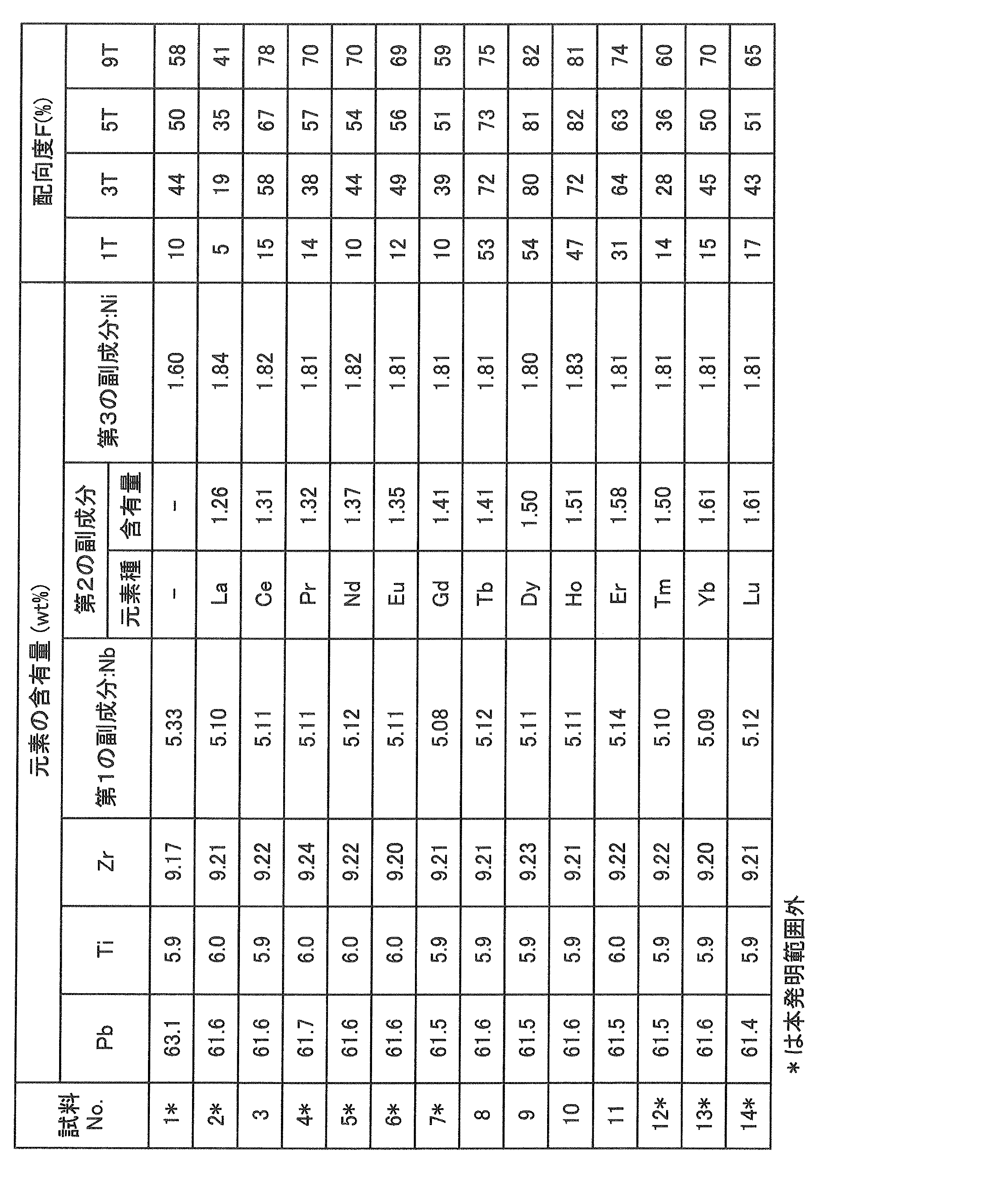
試料番号1は、第2の副成分が含有されていないため、3Tの磁場を印加しても配向度Fは44%であり、結晶配向性に劣っていることが分かった。
試料番号2、4~7、12~14は、第2の副成分としてLa、Pr、Nd、Eu、Gd、Tm、Yb、Luと本発明範囲外の希土類元素が含有されているため、その含有量は0.05wt%以上であるが、3Tの磁場を印加しても配向度Fは19~49%と50%未満であり、結晶配向性に劣ることが分かった。
これに対し試料番号3、8~11は、本発明範囲内のCe、Tb、Dy、Ho、Erを1.31~1.58wt%の範囲で含有している。すなわち、本発明範囲内の希土類元素を0.05wt%以上含有しているので、3Tの磁場印加で配向度Fは58~82%となり、良好な配向性を有することが分かった。
図3は、希土類元素と配向度との関係を示している。横軸は希土類元素の元素種、縦軸は配向度F(%)である。図中、◆印が1T、□印が3T、△印が5T、●印が9Tの各磁場を印加した場合を示している。
この図3から明らかなように本発明範囲内のCe、Tb、Dy、Ho、Erは良好な配向度Fを有しており、9Tの磁場印加では74~82%と極めて大きな配向度Fを得ている。特に、これら本発明範囲内の希土類元素のうちDy、Tbは、印加磁場が1Tであっても50%以上の配向度Fを有しており、より好ましいことが分かった。
これに対し本発明範囲外のLa、Pr、Nd、Eu、Gd、Tm、Yb、Luは配向性に劣ることが分かる。
以上より第2の副成分としては、希土類元素であればよいというのではなく、希土類元素のうち、Ce、Tb、Dy、Ho、Erを選択して使用するのが好ましいことが分かった。
第1の副成分としてのNb、Sbの含有量を異ならせて特性を評価し、また第2及び第3の副成分の添加効果についても調べた。
まず、セラミック素原料として、Pb3O4、TiO2、ZrO2、Nbを含有したNb2O5、Sbを含有したSb2O3、Dy(第2の副成分)を含有したDy2O3、Niを含有したNiO(第3の副成分)を用意した。次いで、これらセラミック素原料を焼結後の元素の含有量が表2となるように秤量した。
そしてその後は、実施例1と同様の方法・手順で、試料番号21~26の試料を作製し、組成分析し、さらに配向度を求めた。
表2は、試料番号21~26の各試料の元素の含有量(wt%)、及び配向度Fを示している。
尚、実施例1と同様、ICP-AES法で検出された元素以外の成分は酸素と見做し、配向度Fは「%」に換算して示している。

試料番号21、25は、Nbの含有量が0.036wt%、0.041wt%と少なく、しかも第2の副成分が含有されていないため、印加磁場が1Tでは配向せず、3Tの磁場を印加しても配向度Fは17%、8%であり、結晶配向性が極端に劣ることが分かった。
試料番号22は、第2の副成分としてのDyの含有量は1.54wt%であるが、Nbの含有量が0.041wt%と少ないため、3~9Tの磁場を印加しても配向度Fは24~30%であり、結晶配向性に劣ることが分かった。
試料番号23は、Nbの含有量は0.613wt%と0.6wt%以上であるが、第2の副成分が含有されていないため、3~5Tの磁場を印加しても配向度Fは12~30%であり、結晶配向性に劣ることが分かった。
これに対し試料番号24は、Nbの含有量は0.628wt%であり、試料番号26は、Nb及びSbの含有量は総計で0.756wt%であり、いずれも0.6wt%以上含有し、また、Dyの含有量も、試料番号24が1.50wt%、試料番号26が1.44wt%であり、いずれも0.05wt%以上であるので、3Tの磁場を印加した場合でも、配向度は56~63%となり、良好な配向性が付与されることが分かった。
以上より、第1の副成分(Nb、Sb)の含有量は0.6wt%以上必要であるが、第1の副成分のみを含有させても所望の配向性を付与することはできず、第1の副成分と第2の副成分の双方を含有させることにより、これらの相乗効果により良好な配向性を付与できることが分かった。
また、第3の副成分であるNiを含有した試料番号24は、Niを含有していない試料番号26に比べて配向度Fを高めることができた。すなわち、第3の副成分を含有させることにより、より一層の配向性向上が可能であることができることが分かった。
第2の副成分としてDyを使用し、Dyの含有量を種々異ならせて特性を評価した。
すなわち、セラミック素原料として、Pb3O4、TiO2、ZrO2、Nb2O5、Dy2O3、NiOを用意した。次いで、これらセラミック素原料を焼結後の元素の含有量が表3となるように秤量した。
そしてその後は、実施例1と同様の方法・手順で、試料番号31~33の試料を作製し、組成分析し、及び配向度を求めた。
表3は、試料番号31~33の各試料の元素の含有量(wt%)、及び配向度Fを示している。また、この表3ではDyを含有していない試料番号1及びDyの含有量が1.50wt%の試料番号9を再掲している。
尚、実施例1と同様、ICP-AES法で検出された元素以外の成分は酸素と見做し、配向度Fは「%」に換算して示している。
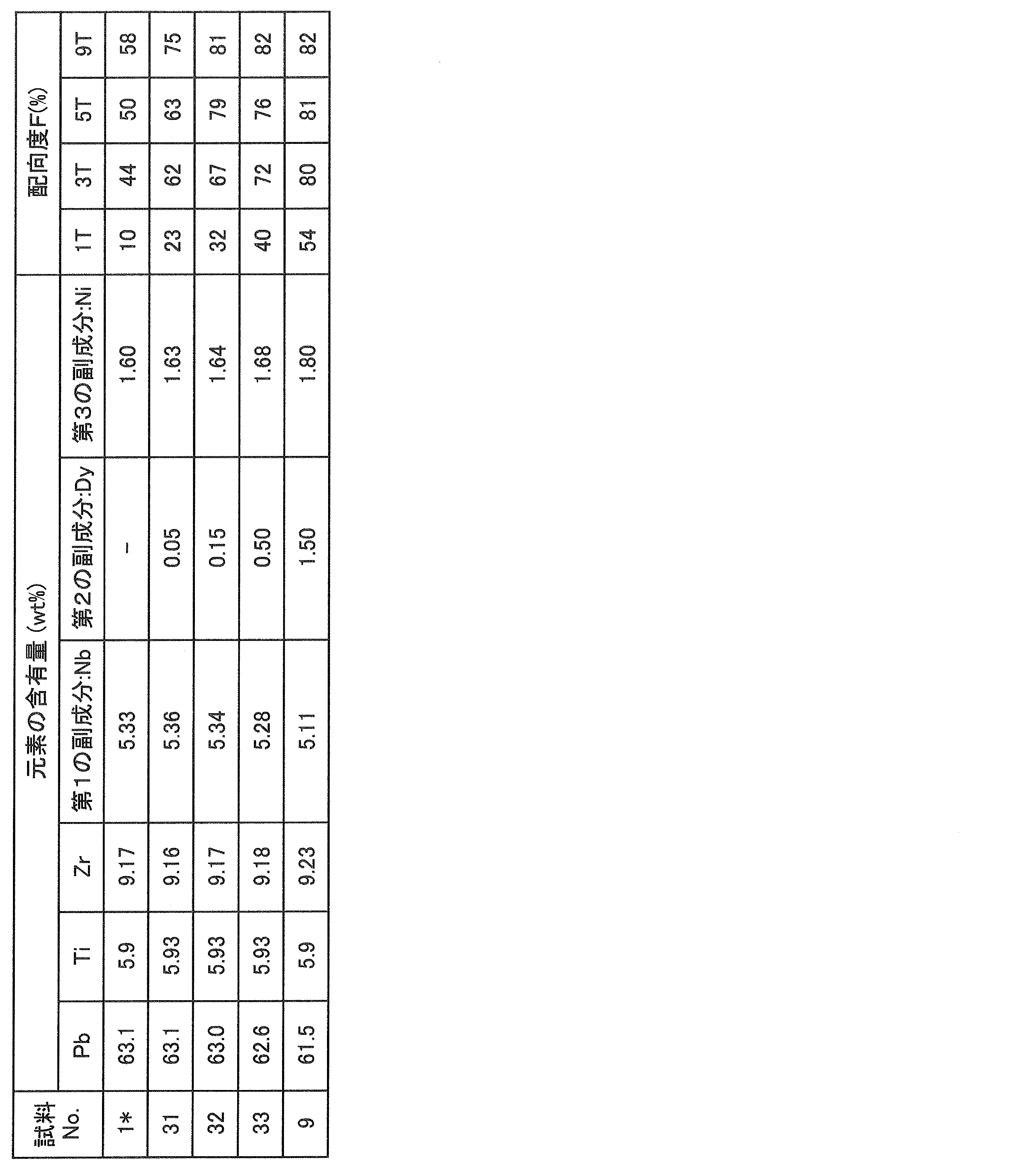
試料番号31~33は、Dyの含有量が0.05~0.50wt%であり、いずれも3Tの磁場を印加した場合に、配向度は62~72%となり、良好な配向性を付与できることが分かった。
すなわち、Dy等の第2の副成分を0.05wt%以上含有していれば、所定量の第1の副成分の添加効果と相俟って高い配向性が付与されたセラミック焼結体が得られることが分かった。
図4は、印加される磁場の大きさと配向度との関係を示す図である。横軸は磁場(T)、縦軸が配向度F(%)である。図中、●印が試料番号1、×印が試料番号31、△印が試料番号32、□印が試料番号33、◆印が試料番号9を示している。
この図4から明らかなように、Dyの含有量が増加するのに伴い、配向度Fも上昇することが分かる。
次に、試料番号31について、EBSD法を使用して配向方位を解析した。
すなわち、試料番号31を切断してその断面を研磨し、この切断面に対し細く絞った電子線を斜め方向から照射し、後方の散乱により電子線の菊池パターンを得た。そして、この菊池パターンを解析して電子線が試料に衝突した箇所の結晶方位を特定した。これを100~1000個の多数の結晶粒子が含まれる広い範囲についてSEMで観察し、EBSD法を使用して解析し、各結晶粒子の結晶方位の分布状態を調べた。
図5は、試料番号31について、磁場の印加方向に対し20°以内の範囲に含まれる{100}配向の分布状態を示すマッピング図である。
また、試料番号31と同一の組成成分の無配向試料についても、上述と同様、EBSD解析を行った。
図6は、その解析結果を示すマッピング図であり、無配向試料について、磁場の印加方向に対し20°以内の範囲に含まれる{100}配向の分布状態を示している。
この図5及び図6では、結晶粒子を白色、灰色、黒色の濃淡で示しており、黒色から灰色にかけての部分が磁場の印加方向に対し20°以内の範囲に{100}配向している結晶粒子を示している。
無配向試料では、図6に示すように、{100}配向している結晶粒子は少なく、磁場の印加方向に対し20°以内の範囲に含まれる{100}配向した結晶粒子の存在比率は、断面積比で16.9%であった。
これに対し試料番号31は、図5に示すように、黒色から灰色で表示される結晶粒子が多く、磁場の印加方向に対し20°以内の範囲に含まれる{100}配向した結晶粒子の存在比率は、断面積比で57.4%であり、試料番号31は、{100}配向していることが確認された。
第3の副成分の元素種及び含有量を種々異ならせて特性を評価した。
すなわち、セラミック素原料として、Pb3O4、TiO2、ZrO2、Nbを含有したNb2O5、Sbを含有したSb2O3、Dyを含有したDy2O3を用意し、第3の副成分を含有したNiO、CoO、Fe2O3、MnO2、MgO、及びZnOをそれぞれ用意した。
そして、これらセラミック素原料を焼結後の元素の含有量が表4となるように秤量し、その後は実施例1と同様の方法・手順で試料番号41~55の試料を作製し、組成分析を行った。
また、主成分100モル部に対する副成分の含有モル量、及び第1の副成分に対する第3の副成分のモル比を組成分析の結果に基づいて算出した。
まず、組成分析で得られた各元素の含有量をそれぞれの原子量で除算して各元素のモル量を算出した。次に、各元素のモル量のうち、Ti元素のモル量とZr元素のモル量との総量と、Pb元素のモル量とを比較し、多い方を主成分のモル量とした。そして、主成分元素(Pb、Ti、Zr)以外の元素のモル量の総計を前記主成分のモル量で除算し、これに100を乗算し、主成分100モル部に対する副成分の含有モル量を算出した。
また、第3の副成分のモル量を、第1の副成分のモル量で除算し、第3の副成分と第1の副成分とのモル比を算出した。
次いで、実施例1と同様の方法・手順で配向度Fを求めた。
表4は、試料番号41~55の各試料の元素の含有量、表5は、試料番号41~55の各試料の第3の副成分と第1の副成分とのモル比、主成分100モル部に対する副成分の含有量総計(モル部)、及び配向度Fを示している。尚、実施例1と同様、ICP-AES法で検出された元素以外の成分は酸素と見做し、配向度Fは「%」に換算して示している。
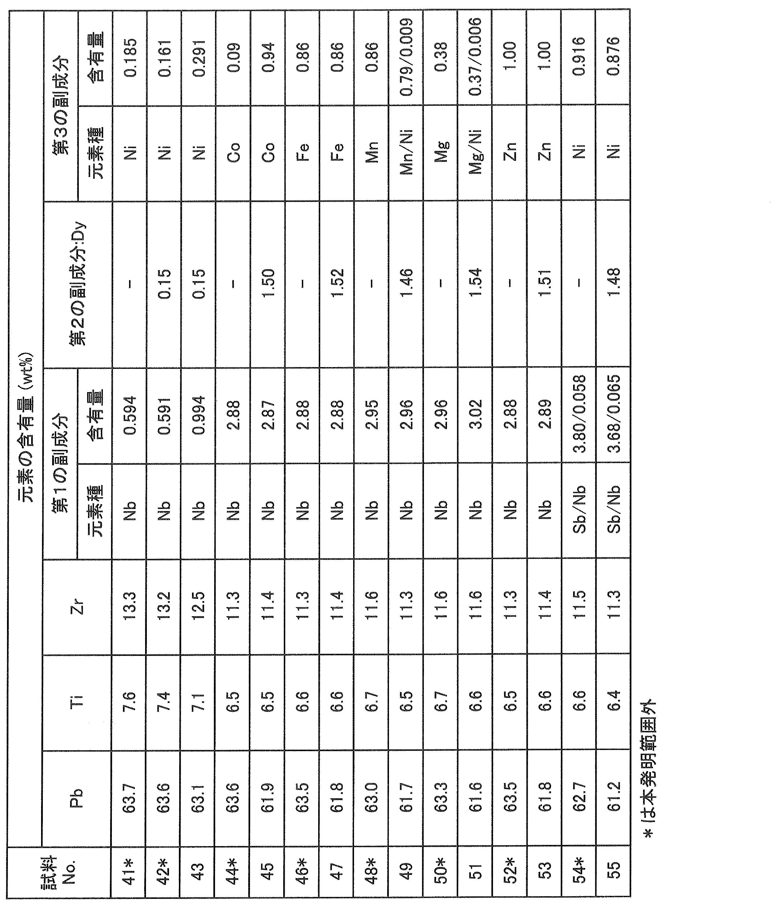
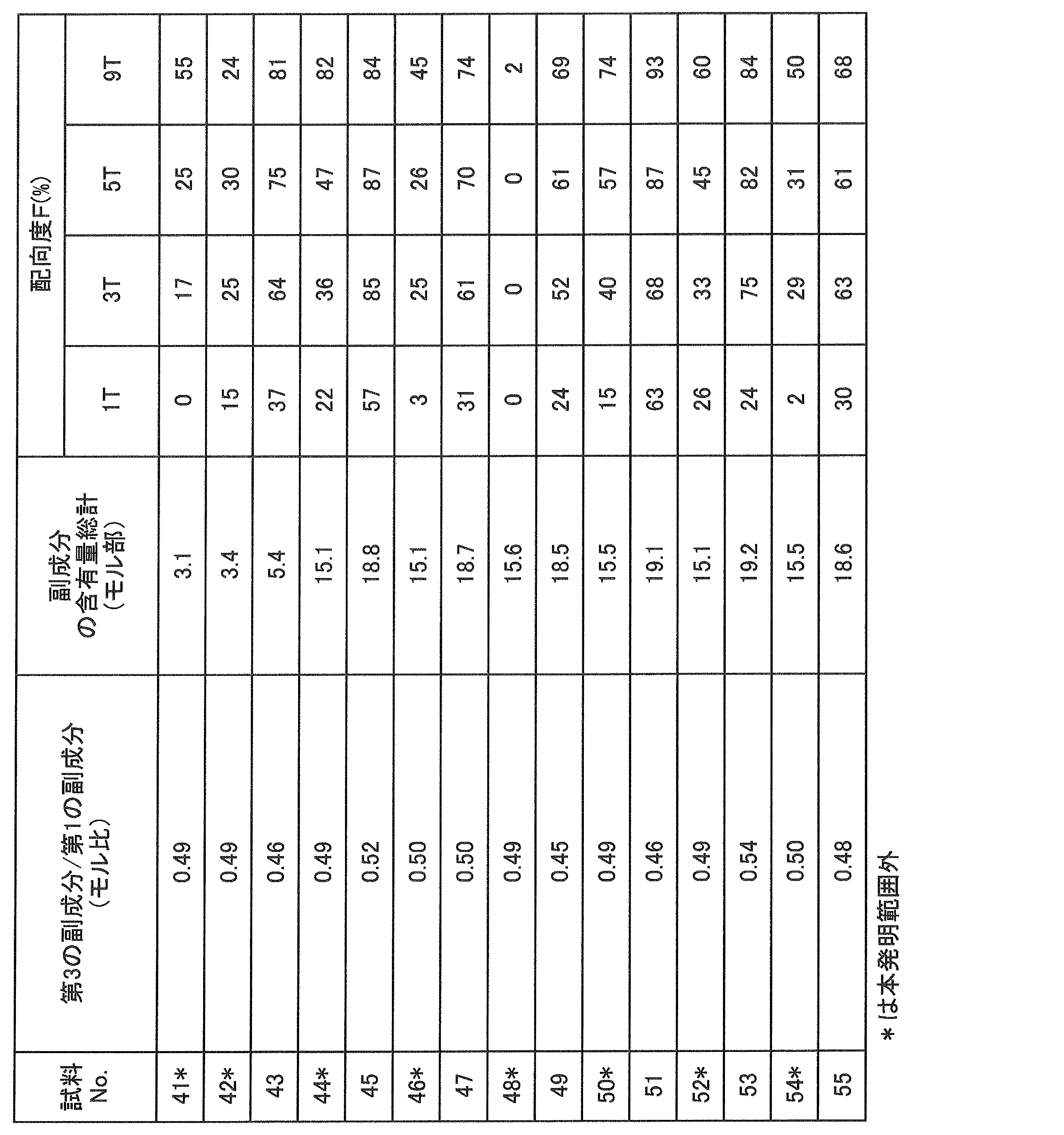
試料番号41は、Nbの含有量は0.594wt%と0.6wt%以下である上に、Niの含有量が0.185wt%と0.29wt%以下であり、しかも第2の副成分が含有されていないため、印加磁場が1Tでは配向せず、3Tの磁場を印加しても配向度Fは17%であり、結晶配向性に劣ることが分かった。
試料番号42は、Dyの含有量は0.15wt%と0.05wt%以上であるが、Nbの含有量が0.591wt%と0.6wt%以下であり、Niの含有量も0.161wt%も少なく、このため3~9Tの磁場を印加しても配向度Fは24~30%と低く、結晶配向性に劣ることが分かった。
試料番号44は、Nbの含有量は0.613wt%と0.6wt%以上であるが、第2の副成分が含有されておらず、第3の副成分としてのCoの含有量も0.09wt%と少なく、このため50%以上の配向度を得るためには9Tの磁場を印加する必要があり、3~5Tの印加磁場では50%未満の配向度Fしか得られなかった。
試料番号46も、Nbの含有量は2.88wt%と0.6wt%以上であり、第3の副成分としてのFeの含有量も0.86wt%と0.29wt%以上であるが、第2の副成分が含有されておらず、このため9Tの磁場を印加しても配向度Fが45%であり、配向性に劣ることが分かった。
試料番号48は、Nbの含有量は2.95wt%と0.6wt%以上であり、第3の副成分としてのMnの含有量も0.86wt%と0.29wt%以上であるが、第2の副成分が含有されておらず、このため5T以下の磁場印加では配向せず、9Tの強磁場を印加しても配向度Fが2%であり、配向性に著しく劣ることが分かった。
試料番号50は、Nbの含有量は2.96wt%と0.6wt%以上であり、第3の副成分としてのMgの含有量も0.86wt%と0.29wt%以上であるが、第2の副成分が含有されておらず、このため印加磁場が3T以下では配向度Fは40%以下であり、50%以上の配向度Fを得るためには5T以上の磁場を印加する必要があることが分かった。
試料番号52は、Nbの含有量は2.88wt%と0.6wt%以上であり、第3の副成分としてのZnの含有量も1.00wt%と0.29wt%以上であるが、第2の副成分が含有されておらず、このため印加磁場が5T以下では配向度Fは50%未満であり、50%以上の配向度Fを得るために9T以上の磁場を印加する必要があることが分かった。
試料番号54は、第1の副成分としてのNb及びSbの含有量の総計は3.858wt%と0.6wt%以上であり、第3の副成分としてのNiの含有量も0.916wt%と0.29wt%以上であるが、第2の副成分が含有されておらず、このため印加磁場が5T以下では配向度Fは50%未満であり、50%以上の配向度Fを得るためには9T以上の強磁場を印加する必要があることが分かった。
これに対し試料番号43、45、47、49、51、53、及び55は、第1の副成分の含有量は0.994~3.745wt%と0.6wt%以上であり、Dyの含有量は0.15~1.54wt%と0.15wt%以上であり、しかも第3の副成分(Ni、Co、Fe、Mn、Mg、Zn)の含有量が0.29wt%以上と本発明の好ましい範囲内であるので、3Tの印加磁場で配向度Fは50%以上と高い配向性を有することが分かった。
特に、試料番号45、51は、1Tの弱磁場を印加した場合であっても57~63%の配向度Fを有する高い配向性を得ることができることが分かった。
また、上述した試料番号43、45、47、49、51、53、及び55は、第3の副成分と第1の副成分とのモル比が0.45~0.54であり、斯かる範囲で主成分100モル部に対し5モル部以上の副成分を含有しても良好な配向性が得られることが分かった。
実施例1の試料番号9及び実施例3の試料番号32を使用し、圧電セラミック電子部品を作製した。
すなわち、試料番号9及び試料番号32について、成形時に磁場を印加した方向を法線とする面で、0.85mm間隔で切断し、厚みが0.85mmで厚み方向に配向したセラミック素体を作製した。
次に、このセラミック素体の両主面にAg電極を形成した後、縦:5mm、横:2.2mmの矩形状に切り出した。このセラミック素体を80℃のシリコンオイル中で厚み方向に2.3kVの電圧を印加し、10分間保持して分極処理を施した。その後、シリコンオイルを洗浄・除去し、圧電セラミック電子部品を得た。
次いで、この圧電セラミック電子部品について、インピーダンスアナライザ(アジレント・テクノロジー社製、4294A)を用い、共振-反共振法を使用して電気機械結合係数k31を測定した。
表6は、試料番号9及び32の電気機械結合係数k31を無配向試料(9′、32′)と共に示している。増加倍率は無配向試料に対するものである。
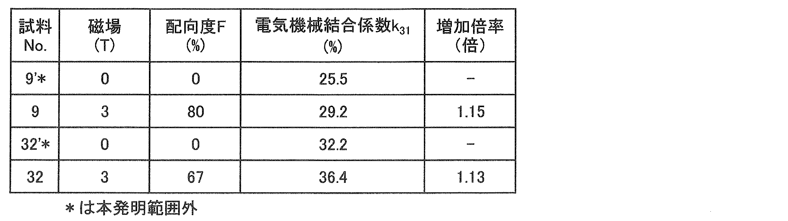
無配向試料である試料番号9′、32′は、電気機械結合係数k31が、それぞれ25.5%、32.2%であった。
これに対し3Tの磁場が印加された試料番号9、32は、配向度Fがそれぞれ87%、67%と高く、このため電気機械結合係数k31は、29.2%、36.4%に上昇し、磁場が印加されなかった無配向試料に比べ、それぞれ増加倍率は1.15倍、1.13倍となった。
このように配向性を高めることにより、より大きな電気機械結合係数k31を有する圧電セラミック電子部品が得られることが分かった。
従来に比べ弱磁場を印加しても十分な結晶配向性を有するセラミック焼結体を得ることができ、またこのセラミック焼結体を使用することにより、より良好な電気機械結合係数を有する圧電セラミック電子部品を得ることができる。
1 圧電セラミック素体
2a、2b 外部電極
3a~3g 内部電極
2a、2b 外部電極
3a~3g 内部電極
Claims (15)
- 一般式AmBO3で表されるペロブスカイト型結晶構造を有する複合酸化物を主成分として含み、
Nb及びSbのうちの少なくとも一方の元素を含む第1の副成分が、0.6wt%以上含有されると共に、
Ce、Tb、Dy、Ho、及びErの中から選択された少なくとも1種の元素を含む第2の副成分が、0.05wt%以上含有され、
結晶粒子の特定の結晶面が、所定方向に配向されていることを特徴とするセラミック焼結体。 - 少なくとも前記第1及び前記第2の副成分を含み、かつ、Ni、Fe、Co、Mn、Mg、及びZnの中から選択された少なくとも1種の元素を含む第3の副成分が、0.29wt%以上含有されていることを特徴とする請求項1記載のセラミック焼結体。
- 前記第1の副成分の含有量に対する前記第3の副成分の含有量は、モル比で0.45~0.54であることを特徴とする請求項2記載のセラミック焼結体。
- 前記主成分以外の副成分の含有量総計は、前記主成分100モル部に対し5モル部以上であることを特徴とする請求項1乃至請求項3のいずれかに記載のセラミック焼結体。
- 前記特定の結晶面は、{100}面であることを特徴とする請求項1乃至請求項4のいずれかに記載のセラミック焼結体。
- 前記特定の結晶面は{100}面であり、ロットゲーリング法による配向度が0.5以上であることを特徴とする請求項1乃至請求項4のいずれかに記載のセラミック焼結体。
- 前記特定の結晶面は{100}面であり、前記結晶粒子の配向は磁場印加によってなされると共に、
前記磁場印加の方向に対し20°以内の範囲で前記結晶粒子の{100}面が前記所定方向に配向している前記結晶粒子の存在比率は、断面積比で50%以上であることを特徴とする請求項1乃至請求項4又は請求項6のいずれかに記載のセラミック焼結体。 - 前記存在比率は、電子線後方散乱回折法に依拠した解析結果に基づいて算出されることを特徴とする請求項7記載のセラミック焼結体。
- 前記複合酸化物は、チタン酸ジルコン酸鉛系化合物であることを特徴とする請求項1乃至請求項8のいずれかに記載のセラミック焼結体。
- 1視野内に前記結晶粒子が100個以上含まれる視野の広さを走査型電子顕微鏡で観察した場合の前記結晶粒子の平均粒子径は、0.5~5μmである請求項1乃至請求項9のいずれかに記載のセラミック焼結体。
- 一般式AmBO3で表されるペロブスカイト型結晶構造を有する複合酸化物を主成分として含み、複数の副成分を含むセラミック焼結体の製造方法であって、
セラミック素原料として、少なくとも前記主成分である元素を含有した複数の原料と、Nb及びSbのうちの少なくとも一方の元素を含む第1の副成分を含有した原料と、Ce、Tb、Dy、Ho、及びErの中から選択された少なくとも1種の元素を含む第2の副成分を含有した原料とを用意し、これらセラミック素原料を秤量する秤量工程と、
前記セラミック素原料と、前記第1及び第2の副成分とを合成した合成物を作製する合成工程と、
前記合成物をスラリー化し、セラミックスラリーを作製するセラミックスラリー作製工程と、
前記セラミックスラリーに磁場を印加しながら成形加工を施し、セラミック成形体を作製する成形体作製工程と、
前記セラミック成形体を焼成する焼成工程とを含み、
前記秤量工程は、前記第1の副成分及び前記第2の副成分の各含有量が焼成後にそれぞれ0.05wt%以上、及び0.6wt%以上となるように、前記セラミック素原料を秤量し、
前記成形体作製工程は、前記セラミックスラリーに印加される磁場が、9T以下であることを特徴とするセラミック焼結体の製造方法。 - 前記セラミックスラリーに印加される磁場は、3~5Tであることを特徴とする請求項11記載のセラミック焼結体の製造方法。
- 前記秤量工程は、Ni、Fe、Co、Mn、Mg、及びZnの中から選択された少なくとも1種の元素を含む第3の副成分を含有した原料を、焼成後における前記第3の副成分の含有量が0.29wt%以上となるように秤量することを特徴とする請求項11又は請求項12記載のセラミック焼結体の製造方法。
- 前記成形体作製工程が、前記セラミックスラリーの搬送方向を軸芯方向とする中空状の電磁石を配して前記セラミックスラリーの面内方向に磁場を印加し、前記セラミックスラリーを前記電磁石の中空部を通過させながら配向処理を施すことを特徴とする請求項11乃至請求項13のいずれかに記載のセラミック焼結体の製造方法。
- 圧電セラミック層を有するセラミック素体の表面に外部電極が形成された圧電セラミック電子部品において、
前記圧電セラミック層は、請求項1乃至請求項10のいずれかに記載のセラミック焼結体で形成されていることを特徴とする圧電セラミック電子部品。
Priority Applications (1)
| Application Number | Priority Date | Filing Date | Title |
|---|---|---|---|
| JP2016532930A JP6264588B2 (ja) | 2014-07-08 | 2015-07-06 | セラミック焼結体の製造方法 |
Applications Claiming Priority (2)
| Application Number | Priority Date | Filing Date | Title |
|---|---|---|---|
| JP2014-140822 | 2014-07-08 | ||
| JP2014140822 | 2014-07-08 |
Publications (1)
| Publication Number | Publication Date |
|---|---|
| WO2016006580A1 true WO2016006580A1 (ja) | 2016-01-14 |
Family
ID=55064211
Family Applications (1)
| Application Number | Title | Priority Date | Filing Date |
|---|---|---|---|
| PCT/JP2015/069445 Ceased WO2016006580A1 (ja) | 2014-07-08 | 2015-07-06 | セラミック焼結体、セラミック焼結体の製造方法及び圧電セラミック電子部品 |
Country Status (2)
| Country | Link |
|---|---|
| JP (1) | JP6264588B2 (ja) |
| WO (1) | WO2016006580A1 (ja) |
Cited By (4)
| Publication number | Priority date | Publication date | Assignee | Title |
|---|---|---|---|---|
| JP2017212399A (ja) * | 2016-05-27 | 2017-11-30 | 京セラ株式会社 | セラミック焼結板および電子部品 |
| JP2020055704A (ja) * | 2018-10-01 | 2020-04-09 | Dowaエレクトロニクス株式会社 | 複合酸化物粉末 |
| JPWO2021039379A1 (ja) * | 2019-08-30 | 2021-03-04 | ||
| WO2024062863A1 (ja) * | 2022-09-22 | 2024-03-28 | 富士フイルム株式会社 | 圧電フィルム |
Citations (4)
| Publication number | Priority date | Publication date | Assignee | Title |
|---|---|---|---|---|
| JP2005100660A (ja) * | 2002-10-24 | 2005-04-14 | Seiko Epson Corp | 強誘電体膜、強誘電体メモリ装置、圧電素子、半導体素子、圧電アクチュエータ、液体噴射ヘッド及びプリンタ |
| JP2008037064A (ja) * | 2006-08-10 | 2008-02-21 | Murata Mfg Co Ltd | 配向性セラミックスの製造方法 |
| JP2012009678A (ja) * | 2010-06-25 | 2012-01-12 | Fujifilm Corp | 圧電体膜、圧電素子および液体吐出装置 |
| WO2013088927A1 (ja) * | 2011-12-12 | 2013-06-20 | 株式会社村田製作所 | 圧電配向セラミックスおよび圧電アクチュエータ |
Family Cites Families (1)
| Publication number | Priority date | Publication date | Assignee | Title |
|---|---|---|---|---|
| JP5676910B2 (ja) * | 2010-04-27 | 2015-02-25 | キヤノン株式会社 | セラミクスの製造方法および圧電材料 |
-
2015
- 2015-07-06 JP JP2016532930A patent/JP6264588B2/ja active Active
- 2015-07-06 WO PCT/JP2015/069445 patent/WO2016006580A1/ja not_active Ceased
Patent Citations (4)
| Publication number | Priority date | Publication date | Assignee | Title |
|---|---|---|---|---|
| JP2005100660A (ja) * | 2002-10-24 | 2005-04-14 | Seiko Epson Corp | 強誘電体膜、強誘電体メモリ装置、圧電素子、半導体素子、圧電アクチュエータ、液体噴射ヘッド及びプリンタ |
| JP2008037064A (ja) * | 2006-08-10 | 2008-02-21 | Murata Mfg Co Ltd | 配向性セラミックスの製造方法 |
| JP2012009678A (ja) * | 2010-06-25 | 2012-01-12 | Fujifilm Corp | 圧電体膜、圧電素子および液体吐出装置 |
| WO2013088927A1 (ja) * | 2011-12-12 | 2013-06-20 | 株式会社村田製作所 | 圧電配向セラミックスおよび圧電アクチュエータ |
Cited By (7)
| Publication number | Priority date | Publication date | Assignee | Title |
|---|---|---|---|---|
| JP2017212399A (ja) * | 2016-05-27 | 2017-11-30 | 京セラ株式会社 | セラミック焼結板および電子部品 |
| JP2020055704A (ja) * | 2018-10-01 | 2020-04-09 | Dowaエレクトロニクス株式会社 | 複合酸化物粉末 |
| JP7194547B2 (ja) | 2018-10-01 | 2022-12-22 | Dowaエレクトロニクス株式会社 | 複合酸化物粉末 |
| JPWO2021039379A1 (ja) * | 2019-08-30 | 2021-03-04 | ||
| WO2021039379A1 (ja) * | 2019-08-30 | 2021-03-04 | 国立研究開発法人産業技術総合研究所 | 配向度分布計算方法、配向度分布解析装置および配向度分布解析プログラム |
| JP7460180B2 (ja) | 2019-08-30 | 2024-04-02 | 国立研究開発法人産業技術総合研究所 | 配向度分布計算方法、配向度分布解析装置および配向度分布解析プログラム |
| WO2024062863A1 (ja) * | 2022-09-22 | 2024-03-28 | 富士フイルム株式会社 | 圧電フィルム |
Also Published As
| Publication number | Publication date |
|---|---|
| JPWO2016006580A1 (ja) | 2017-04-27 |
| JP6264588B2 (ja) | 2018-01-24 |
Similar Documents
| Publication | Publication Date | Title |
|---|---|---|
| Huang et al. | Giant electrostrictive effect in lead-free barium titanate-based ceramics via A-site ion-pairs engineering | |
| Hou et al. | Effect of Li2CO3 addition on the dielectric and piezoelectric responses in the low-temperature sintered 0.5 PZN–0.5 PZT systems | |
| Zhang et al. | Improved Electrical Properties of Low-Temperature Sintered Cu Doped BaCaZrTiO Ceramics. | |
| Kushvaha et al. | Structural, piezoelectric and highdensity energy storage properties of lead-free BNKT-BCZT solid solution | |
| Cheng et al. | Enhanced piezoelectric properties and thermal stability of Bi0. 5Na0. 5TiO3 modified BiFeO3BaTiO3 ceramics with morphotropic phase boundary | |
| US10964878B2 (en) | Piezoelectric composition and piezoelectric device | |
| JP6264588B2 (ja) | セラミック焼結体の製造方法 | |
| EP3085678B1 (en) | Piezoelectric ceramic, manufacturing method therefor, and electronic component | |
| Yang et al. | Acceptor doping and actuation mechanisms in Sr-doped BiFeO3BaTiO3 ceramics | |
| Cen et al. | Improving the piezoelectric strain and anti-reduction properties of K 0.5 Na 0.5 NbO 3-based ceramics sintered in a reducing atmosphere | |
| Peng et al. | Effect of doping Mn/Fe/Co on the ferroelectric properties and depolarization behavior of BNT ceramics | |
| Bochenek et al. | Strengthening the ferroelectric properties in the three-component multiferroic ceramic composites | |
| WO2023112661A1 (ja) | 圧電/誘電体セラミックス、圧電素子及び発音体 | |
| US10811591B2 (en) | Piezoelectric composition and piezoelectric device | |
| Kumar et al. | Sol–gel synthesis and characterization of a new four-layer K0. 5Gd0. 5Bi4Ti4O15 Aurivillius phase | |
| Pahuja et al. | Novel method of synthesis of multiferroic nickel cobalt ferrite–barium strontium titanate composite system | |
| JP6094951B2 (ja) | 強磁性誘電体材料、強磁性誘電体材料の製造方法、及びセラミック電子部品 | |
| Wu et al. | Optimization of piezoelectric properties of 0.7 BiFeCo0. 004O3-0.3 BaTiO3 ceramics by adjusting dwell time during the sintering process | |
| Zhang et al. | Improved electrical properties of low-temperature sintered Cu doped Ba0. 99Ca0. 01Zr0. 02Ti0. 98O3 ceramics | |
| JPWO2015025589A1 (ja) | 酸化物セラミックス、及びセラミック電子部品 | |
| Zeng et al. | Structure, dielectric, and multiferroic properties of Bi0. 85Nd0. 15Fe0. 98Zr0. 02O3 in Ba and Ti co-doping | |
| Wang | Preparation of barium titanate-based ferroelectric ceramics by solid-phase sintering and its energy storage performance | |
| CN109809493A (zh) | 新型铋铁氧室温多铁磁电耦合材料及制备方法、电子器件 | |
| WO2023063007A1 (ja) | 積層型圧電素子 | |
| CN113402274B (zh) | 压电组合物及电子部件 |
Legal Events
| Date | Code | Title | Description |
|---|---|---|---|
| 121 | Ep: the epo has been informed by wipo that ep was designated in this application |
Ref document number: 15818864 Country of ref document: EP Kind code of ref document: A1 |
|
| ENP | Entry into the national phase |
Ref document number: 2016532930 Country of ref document: JP Kind code of ref document: A |
|
| NENP | Non-entry into the national phase |
Ref country code: DE |
|
| 122 | Ep: pct application non-entry in european phase |
Ref document number: 15818864 Country of ref document: EP Kind code of ref document: A1 |