WO2016006277A1 - 端子部材、電気コネクタ、及び電磁クラッチ - Google Patents
端子部材、電気コネクタ、及び電磁クラッチ Download PDFInfo
- Publication number
- WO2016006277A1 WO2016006277A1 PCT/JP2015/057791 JP2015057791W WO2016006277A1 WO 2016006277 A1 WO2016006277 A1 WO 2016006277A1 JP 2015057791 W JP2015057791 W JP 2015057791W WO 2016006277 A1 WO2016006277 A1 WO 2016006277A1
- Authority
- WO
- WIPO (PCT)
- Prior art keywords
- slit
- press
- terminal member
- connection piece
- electrical connector
- Prior art date
- Legal status (The legal status is an assumption and is not a legal conclusion. Google has not performed a legal analysis and makes no representation as to the accuracy of the status listed.)
- Ceased
Links
Images







Classifications
-
- B—PERFORMING OPERATIONS; TRANSPORTING
- B60—VEHICLES IN GENERAL
- B60H—ARRANGEMENTS OF HEATING, COOLING, VENTILATING OR OTHER AIR-TREATING DEVICES SPECIALLY ADAPTED FOR PASSENGER OR GOODS SPACES OF VEHICLES
- B60H1/00—Heating, cooling or ventilating devices
- B60H1/32—Cooling devices
-
- F—MECHANICAL ENGINEERING; LIGHTING; HEATING; WEAPONS; BLASTING
- F16—ENGINEERING ELEMENTS AND UNITS; GENERAL MEASURES FOR PRODUCING AND MAINTAINING EFFECTIVE FUNCTIONING OF MACHINES OR INSTALLATIONS; THERMAL INSULATION IN GENERAL
- F16D—COUPLINGS FOR TRANSMITTING ROTATION; CLUTCHES; BRAKES
- F16D27/00—Magnetically- or electrically- actuated clutches; Control or electric circuits therefor
- F16D27/10—Magnetically- or electrically- actuated clutches; Control or electric circuits therefor with an electromagnet not rotating with a clutching member, i.e. without collecting rings
-
- H—ELECTRICITY
- H01—ELECTRIC ELEMENTS
- H01R—ELECTRICALLY-CONDUCTIVE CONNECTIONS; STRUCTURAL ASSOCIATIONS OF A PLURALITY OF MUTUALLY-INSULATED ELECTRICAL CONNECTING ELEMENTS; COUPLING DEVICES; CURRENT COLLECTORS
- H01R4/00—Electrically-conductive connections between two or more conductive members in direct contact, i.e. touching one another; Means for effecting or maintaining such contact; Electrically-conductive connections having two or more spaced connecting locations for conductors and using contact members penetrating insulation
- H01R4/24—Connections using contact members penetrating or cutting insulation or cable strands
Definitions
- the present invention relates to a terminal member having a slit into which a lead is press-fitted, an electric connector including the terminal member, and an electromagnetic clutch including the terminal member or the electric connector.
- a conducting wire connecting terminal member As an example of a terminal member having a slit into which a conducting wire is press-fitted, a conducting wire connecting terminal member described in Patent Document 1 is known.
- the conductor connecting terminal member has a connecting piece in which a plurality of slits are formed, and after the conducting wire is arranged in the case of the upper surface opening, the connecting piece is press-fitted into the mounting groove of the case.
- the conductive wire is press-fitted and connected to the plurality of slits.
- the width of the connecting piece in the longitudinal direction is larger than the width of the mounting groove. Therefore, when the connection piece is mounted in the mounting groove, the width of the slit is reduced, for example, the width of the connection piece is formed larger and / or the width of the mounting groove is formed smaller. In such a case, the conductor may be damaged more than necessary or disconnected.
- an object of the present invention is to provide a terminal member that can be reliably connected to a conductive wire without damaging or breaking the conductive wire more than necessary, and an electrical connector including the terminal member.
- a terminal member having a connection piece portion formed with at least one first slit into which a conducting wire is press-fitted and having the connection piece portion mounted in a concave attachment portion.
- a width dimension between both side edges of the connection piece portion sandwiching the at least one first slit is set larger than a corresponding inner dimension of the attachment portion, and the connection piece portion includes A suppressing portion is formed that suppresses the width of the at least one first slit from being narrowed when the connecting piece is mounted in the mounting portion.
- the connection includes a resin-made housing having a recess, and a connection piece portion in which at least one first slit into which a conducting wire is press-fitted is formed, and sandwiches the at least one first slit.
- an electrical connector having both ends of one part fixed to a pair of opposing wall portions forming the concave portion of the housing, and the housing is inserted into a predetermined insertion hole.
- a dimension between outer surfaces of the pair of opposing wall portions of the housing is set larger than a corresponding inner dimension of the insertion hole, and the housing is inserted into the insertion hole in the connection piece portion.
- a suppressing portion that suppresses the width of the at least one first slit from being narrowed is formed.
- the terminal member while being held in the mounting portion without rattling, it is suppressed that the width of the at least one first slit is narrowed when the connection piece portion is mounted in the mounting portion. .
- the said connection piece part can be reliably connected to a conducting wire, without damaging a conducting wire more than necessary or making it break.
- the insertion hole is smoothly inserted, and the width of the at least one first slit is suppressed from being narrowed when the housing is inserted into the insertion hole. For this reason, it can connect reliably to a conducting wire via the said connection piece part, without damaging a conducting wire more than necessary, or making it break.
- FIG. 1 is an overall schematic diagram of an electromagnetic coil unit according to a first embodiment. It is a principal part disassembled perspective view of the electromagnetic coil unit by the said 1st Embodiment. It is a figure which shows the cable for electric power feeding. It is a figure which shows the inside of the case made from insulating resin. It is a perspective view which shows the state by which the connection piece part of the terminal member attached to the said cable was mounted
- FIG. 1 and 2 show a first embodiment of an electromagnetic coil unit (field core / coil assembly) of an electromagnetic clutch to which the present invention is applied.
- the electromagnetic clutch is incorporated in, for example, a compressor constituting a vehicle air conditioner, and intermittently transmits the power of a vehicle engine or motor as a drive source to the compressor as a driven device. That is, the electromagnetic clutch is an electromagnetic clutch of a vehicle compressor.
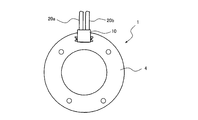
- FIG. 1 is an overall schematic view of an electromagnetic coil unit 1 according to the first embodiment
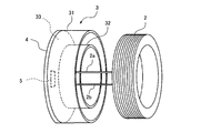
- FIG. 2 is an exploded perspective view of a main part of the electromagnetic coil unit 1.
- the electromagnetic coil unit 1 includes an electromagnetic coil 2 wound in a ring shape and a cylindrical ring body (field core) 3 that accommodates the electromagnetic coil 2.
- the ring body 3 includes an outer cylindrical portion 31, an inner cylindrical portion 32 arranged concentrically with the outer cylindrical portion 31, and a ring that connects the outer cylindrical portion 31 and the inner cylindrical portion 32 at one end side.
- the ring body 3 accommodates the electromagnetic coil 2 wound in a ring shape in a space formed by the outer cylindrical portion 31, the inner cylindrical portion 32, and the connecting portion 33.
- the space is filled with a resin material (not shown) after the electromagnetic coil 2 is accommodated, and the electromagnetic coil 2 is sealed by the filled resin material, and the electromagnetic coil 2 and the ring body 3 are integrated. It becomes.
- a mounting plate 4 for attaching the electromagnetic coil unit 1 to a predetermined place is fixed to the outer surface of the connecting portion 33 of the ring body 3, and the connecting portion 33 and the mounting plate 4 have through holes penetrating them. 5 is formed (see FIG. 2).
- An insulating resin case 10 is fixed to the outer surface of the mounting plate 4 (the surface opposite to the connecting portion 33) so as to cover the through hole 5 (see FIG. 1).
- Both end portions 2b and 2b of the electromagnetic coil 2 accommodated in the space are led to the outside through the through hole 5 and are introduced into the case 10 through the bottom of the case 10. Are connected to cables 20a and 20b.
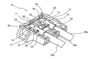
- FIG. 3 shows the cables 20a and 20b.
- a conductive terminal member 21 is attached to the ends of the cables 20a and 20b.
- the terminal member 21 includes a crimping portion 22 that is caulked and connected to the cable 20a (20b), and a connection piece portion 23 that is connected to a conducting wire.
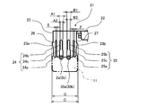
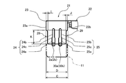
- the connection piece portion 23 is formed in a substantially U-shaped cross section downward, and a slit (hereinafter referred to as “press-fit slit”) 24 into which a conducting wire is press-fitted into each of a pair of opposed flat portions. 25, and slits 26 and 27 (hereinafter referred to as “non-press-fit slits”) into which the conducting wire is not press-fitted are formed.
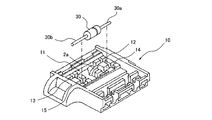
- FIG. 4 is a view showing the inside of the case 10.
- the case 10 is formed in a box shape whose upper surface is open, and has a concave attachment portion 11 to which the connection piece portion 23 of the terminal member 21 attached to the cables 20a and 20b is attached.
- first to fourth groove portions 12 to 15 into which conductive wires are fitted are provided.
- one end 2 a of the electromagnetic coil 2 extending through the bottom surface of the case 10 is fitted into the first groove 12.
- the other end 2 b of the electromagnetic coil 2 extending through the bottom surface of the case 10 is fitted into the second groove 13.
- one lead wire 30 a of the back surge absorbing diode 30 is fitted into the third groove portion 14, and the other lead wire 30 b of the diode 30 is fitted into the fourth groove portion 15.
- connection piece 23 of the terminal member 21 attached to the cable 20 a is mounted in the attachment portion 11 of the case 10, so that one end of the cable 20 a and the electromagnetic coil 2 is obtained. 2 a and one lead wire 30 a of the diode 30 are connected via the terminal member 21.
- connection piece portion 23 of the terminal member 21 attached to the cable 20b is attached to the attachment portion 62 of the case 6, so that the other end portion 2b of the electromagnetic coil 2 and the other end of the diode 30 are connected.
- the lead wire 30 b is connected via the terminal member 21.
- the case 10 is filled with a resin material after the terminal members 21 of the cables 20a and 20b are mounted, and the terminal member 21 is sealed with the filled resin material.
- the electromagnetic coil 2 is accommodated in the space of the ring body 3, and then the space is filled with a resin material. At this time, both end portions 2 a and 2 b of the electromagnetic coil 2 are drawn out from the through hole 5 to the outside of the ring body 3, and are inserted into an insertion hole (not shown) formed in the bottom surface of the case 10 and guided into the case 10.
- one end 2 a of the electromagnetic coil 2 is fitted into the first groove 12, and the other end 2 b of the electromagnetic coil 2 is fitted into the second groove 13.
- both end portions 2a and 2b of the electromagnetic coil 2 are bent in opposite directions after passing through the bottom surface of the case 10.
- one lead wire 30 a of the diode 30 is fitted into the third groove portion 14, and the other lead wire 20 b of the diode 30 is fitted into the fourth groove portion 15.
- connection piece portion 23 of the terminal member 21 attached to the cables 20 a and 20 b is set on the upper portion of the attachment portion 11 of the case 10.
- one press-fit slit 24 formed in the connection piece 23 is arranged on the end 2 a or 2 b of the electromagnetic coil 2, and the other press-fit slit 25 is arranged on the lead wire 30 a or 30 b of the diode 30. .
- one press-fit slit 24 includes a wide portion 24a on the opening end side, a narrow portion 24b on the back side, and a taper portion 24c that connects them. It is formed.
- the width A1 of the wide portion 24a is set slightly smaller than the wire diameter of the electromagnetic coil 2, and the width A2 of the narrow portion 242 is set to be smaller than the width A1 of the wide portion 24a.
- the other press-fit slit 25 has a wide portion 25a on the opening end side, a narrow portion 25b on the back side, and a tapered portion 25c that connects them.
- the width B1 of the wide portion 25a is set slightly smaller than the lead wire diameter of the diode 30, and the width B2 of the narrow portion 25b is set to be smaller than the width B1 of the wide portion 25a.
- the width C between the side edges 23a and 23b of the connection piece 23 sandwiching the press-fit slits 24 and 25 is larger than the corresponding inner dimension (distance between inner walls) D of the mounting portion 11 provided in the case 10. Is set.
- the non-press-fit slits 26 and 27 are arranged with the press-fit slits 24 and 25 interposed therebetween, that is, arranged outside the press-fit slits 24 and 25.
- one non-press-fit slit 26 is formed at a position closer to the side edge portion 23a adjacent to the adjacent press-fit slit 24, and the other non-press-fit slit 27 is adjacent to the press-fit slit 24. It is formed at a position closer to the side edge 23 b adjacent to the slit 25.
- connection piece 23 set on the upper part of the attachment part 11 of the case 10 is pushed down, the connection piece 23 is mounted (fitted) in the attachment part 11 as shown in FIG.
- the end 2a (2b) of the electromagnetic coil 2 is press-fitted into the narrow portion 24b of one press-fit slit 24 formed in the connection piece 23, and the diode 30 is inserted into the narrow portion 25b of the other press-fit slit 25.
- the lead wire 30a (30b) is press-fitted.
- the cable 20a is connected to one end 2a of the electromagnetic coil 2 and one lead wire 30a of the diode 30 via the terminal member 21.
- the cable 20b and the other end of the electromagnetic coil 2 are connected.
- the part 2 b and the other lead wire 30 b of the diode 30 are connected via the terminal member 21.
- the depth (length) G of the non-press-fit slits 26 and 27 is the press-fit slit 24 of the conducting wire (the end portions 2a and 2b of the electromagnetic coil 2 and the lead wires 30a and 30b of the diode 30).
- the case 10 is filled with a resin material, the terminal member 21 is sealed, and the opening of the upper surface of the case 10 is covered with a lid member (not shown) to complete the assembly of the electromagnetic coil unit 1.
- the width C between the side edges 23a and 23b of the connection piece 23 is set to be larger than the corresponding inner dimension D of the concave mounting portion 11 provided in the case 10. For this reason, the connecting piece 23 is press-fitted into the mounting portion 11, and the connecting piece 23 and thus the terminal member 21 are held in the case 10 without rattling.
- the end portions 2a and 2b of the electromagnetic coil 2 are press-fitted into one press-fitting slit 24 (more specifically, the narrow portion 24b) formed in the connection piece 23, and the lead wires 30a and 30b of the diode 30 are Since the other press-fitting slit 25 (more specifically, the narrow portion 25b) formed in the connection piece 23 is press-fitted, the terminal member 21, the electromagnetic coil 2 and the diode 30 are securely connected. .
- non-press-fit slits 26 and 27 are formed in the connection piece 23 so as to sandwich them.
- the widths of the press-fit slits 24, 25 are reduced by the force that the side edges 23 a, 23 b of the connecting piece 23 receive from the inner wall of the mounting portion 11. Narrowing is suppressed. That is, when the side edge portions 23a and 23b of the connection piece 23 receive a force from the inner wall of the mounting portion 11, first, the portion of the connection piece 23 located outside the non-press-fit slits 26 and 27 is deformed (bends).
- the width of the press-fit slits 24 and 25 is suppressed from being narrowed. Thereby, the possibility that the ends 2a and 2b of the electromagnetic coil 2 and the lead wires 30a and 30b of the diode 30 are damaged more than necessary or disconnected is greatly reduced. Therefore, in this embodiment, the non-press-fit slits 26 and 27 correspond to the “suppressing part” of the present invention.
- the total value (E + F) of the width E of the non-press-fit slit 26 and the width F of the non-press-fit slit 27 is determined from the width C between the side edges 23a and 23b of the connecting piece 23. 11 is set to a value (C ⁇ D) or more obtained by subtracting the corresponding inner dimension D. For this reason, it is more reliably prevented that the ends 2a and 2b of the electromagnetic coil 2 and the lead wires 30a and 30b of the diode 30 are damaged more than necessary or disconnected.
- connection piece 23 has two non-press-fit slits 26 and 27 arranged so as to sandwich the two press-fit slits 24 and 25.
- the connection piece 23 may be configured to have only one of the non-press-fit slits 26 and 27.
- the non-press-fit slit is formed at the side edge 23a or the portion of the connecting piece 23 closer to the side edge 23b than the two press-fit slits 24, 25, and the width of the non-press-fit slit is equal to the side edges 23a.
- connection piece portion 23 is preferably set to be equal to or greater than a value obtained by subtracting the corresponding inner dimension D of the mounting portion 11 from the width dimension C (C ⁇ D).
- the connection piece portion 23 has two press-fit slits 24 and 25.
- the connection piece portion 23 may have one press-fit slit, or three or more. It may be.
- both side edge portions 23a and 23b of the connection piece portion 23 protrude outward, but as shown in FIG. 9, both side edge portions 23a and 23b of the connection piece portion 23. May have a shape without protrusions.
- the connecting piece portion 23 is formed by notching the portions corresponding to the press-fit slits 24, 25 of the side edge portions 23 a, 23 b, instead of the non-press-fit slits 26, 27. 29 may be included.
- the total value (I + J) of the width I of the notch 28 and the width J of the notch 29 is determined from the width C between the side edges 23a and 23b of the connecting piece 23.
- FIG. 11 and 12 show a second embodiment of an electromagnetic coil unit (field core / coil assembly) of an electromagnetic clutch to which the present invention is applied.
- FIG. 11 is a cross-sectional view of the electromagnetic coil unit 50 according to the second embodiment
- FIG. 12 is an exploded perspective view of the electromagnetic coil unit 50.
- the electromagnetic coil unit 50 includes a bobbin 52 around which the electromagnetic coil 51 is wound, an electrical connector 53 attached to the bobbin 52, and a cylindrical ring body (field core) 54 that houses the bobbin 52.
- the bobbin 52 includes a cylindrical portion 521 around which the electromagnetic coil 51 is wound, and flange portions 522a and 522b provided at both ends of the cylindrical portion 521.
- a cutout portion 523 is formed on a part of the outer periphery of the one flange portion 522a, and a connector mounting portion 524 to which the electric connector 53 is attached is formed on the outer surface of the one flange portion 522a. 523 is provided therebetween.
- Connector mounting portion 524 has a left side portion located on the left side of notch portion 523 when viewed from the outside of flange portion 522a, and a right side portion located on the right side of notch portion 523.
- FIG. 13 is an enlarged view of the connector mounting portion 524.
- the connector mounting portion 524 is provided with first to fourth groove portions 525 to 528 into which the conductive wires are fitted.
- the first groove portion 525 and the third groove portion 527 are provided in the left portion of the connector attachment portion 524, and the second groove portion 526 and the fourth groove portion 528 are provided in the right portion of the connector attachment portion 524.
- one end of the electromagnetic coil 51 wound around the bobbin 52 (the outer peripheral surface of the cylindrical portion 521 thereof) is fitted in the first groove portion 525, and the second groove portion 526 has the cylindrical portion 521 of the cylindrical portion 521.
- the other end of the electromagnetic coil 51 wound around the outer peripheral surface is fitted.
- the one end portion of the electromagnetic coil 51 wound around the bobbin 52 is pulled out to the outside of the flange portion 522 a through the notch portion 523, fitted into the first groove portion 525, and wound around the bobbin 52.
- the other end of the electromagnetic coil 51 is pulled out to the outside of the flange portion 522a through the notch portion 523 and fitted into the second groove portion 526.
- one lead wire of a back surge absorbing diode (not shown) is fitted into the third groove portion 527, and the other lead wire of the diode is fitted into the fourth groove portion 528.
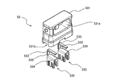
- FIG. 14 and 15 show the electrical connector 53.
- FIG. 14 is an exploded perspective view of the electrical connector 53
- FIG. 15 is an enlarged cross-sectional view of the electrical connector 53.
- the electrical connector 53 is formed by insert molding, and includes a resin housing 531 and a pair of terminal members 532 and 532.
- the housing 531 has an outer peripheral surface in a predetermined range on the bottom side that is formed one step higher than the outer peripheral surface of the other part.
- the housing 531 has a first recess 531a formed on one side surface and a second recess 531b formed on the bottom surface.
- the terminal member 532 has a first connection piece portion 533 connected to a power supply cable terminal or the like, a second connection piece portion 534 to which a conducting wire is connected, and a connection portion 535 for connecting them.
- the first connection piece 533 is formed in a flat plate shape, and protrudes from the bottom of the first recess 531 a toward the side of the housing 531 in the first recess 531 a of the housing 531.
- the second connection piece 534 is formed in a substantially U shape with the cross section downward.
- the second connection piece portion 534 is fixed (buried) to the inner surfaces 531c and 531d of the pair of opposing wall portions that form the second concave portion 531b of the housing 531 between the both end portions.
- the intermediate part is exposed in the second recess 531b.
- the connecting portion 535 is also buried in the housing 531.
- press-fitting slits 536 and 537 into which a lead is press-fitted and non-press-fit slits 538 and 539 into which the lead is not press-fitted are formed.
- One press-fitting slit 536 is formed to have a wide portion 536a on the opening end side, a narrow portion 536b on the back side, and a tapered portion 536c connecting them.
- the width A1 'of the wide portion 536a is set slightly smaller than the wire diameter of the electromagnetic coil 51, and the width A2' of the narrow portion 536b is set smaller than the width A1 'of the wide portion 536a.
- the other press-fit slit 537 has a wide portion 537a on the opening end side, a narrow portion 537b on the back side, and a tapered portion 537c connecting them.
- the width B1 'of the wide portion 537a is set slightly smaller than the lead wire diameter of the diode, and the width B2' of the narrow portion 537b is set smaller than the width B1 'of the wide portion 537a.
- the non-press-fit slits 538 and 539 are arranged with the press-fit slits 536 and 537 interposed therebetween, that is, arranged outside the press-fit slits 536 and 537. More specifically, one non-press-fit slit 538 is formed at a position closer to the inner surface 531 c of the opposing wall portion adjacent to the adjacent press-fit slit 536, and the other non-press-fit slit 539 is formed from the adjacent press-fit slit 537. Is also formed at a position close to the inner surface 531d of the adjacent opposing wall portion.
- the electrical connector 53 is attached to the connector attachment portion 524 provided on the bobbin 52 from the bottom surface side. Specifically, the electrical connector 53 is attached to the bobbin 52 by fitting the second recess 531b of the housing 531 of the electrical connector 53 into the connector attachment portion 524 (the outer periphery thereof). By attaching the electrical connector 53 to the bobbin 52, one terminal member 532 of the electrical connector 53 is connected to one end of the electromagnetic coil 51 and one lead wire of the diode, and the other terminal member 532 is connected to the electromagnetic coil. 51 is connected to the other end of 51 and the other lead of the diode.
- the ring body 54 includes an outer cylindrical portion 541, an inner cylindrical portion 542 disposed concentrically with the outer cylindrical portion 541, an outer cylindrical portion 541 and an inner cylindrical portion 542. And an annular plate-like connecting portion 543 connected at one end side.
- a through hole 544 having a size corresponding to the electrical connector 53 is formed in the connecting portion 543.
- the through hole 544 has an opening area that is larger than the cross-sectional area on the upper surface side of the electrical connector 53 (housing 531) and smaller than the cross-sectional area of the predetermined range on the bottom surface side.
- An attachment plate 55 for attaching the electromagnetic coil unit 50 to a predetermined place is fixed to the outer surface of the connecting portion 543.
- the ring body 54 accommodates the bobbin 52 to which the electrical connector 53 is attached in a ring-shaped space formed by the outer cylindrical portion 541, the inner cylindrical portion 542, and the connecting portion 543. Specifically, the ring body 54 has the bobbin 52 in the space in a state where the upper surface side of the electrical connector 53 is exposed to the outside through the through hole 544, that is, in a state where the electrical connector 53 is inserted into the through hole 544. Accommodate. The space is filled with a resin material (not shown) after the bobbin 52 is accommodated.
- the electromagnetic coil 51 is wound around and fixed to the outer peripheral surface of the cylindrical portion 521 of the bobbin 52, and both ends of the electromagnetic coil 51 are moved from the notch portion 523 formed in the flange portion 522a of the bobbin 52 to the outside of the flange portion 522a. Pull out.
- one end of the electromagnetic coil 51 is fitted into the first groove 525 provided in the left portion of the connector mounting portion 524, and the other end of the electromagnetic coil 51 is connected to the right portion of the connector mounting portion 524. It fits into the second groove 526 provided. At this time, both end portions of the electromagnetic coil 51 are bent in opposite directions.
- one lead wire of the diode is fitted into a third groove portion 527 provided in the left side portion of the connector mounting portion 524, and the other lead wire of the diode is provided in the right side portion of the connector mounting portion 524. Fit into the fourth groove 528.
- the electrical connector 53 is set on the upper part of the connector mounting portion 524 provided on the outer surface of the flange portion 522a of the bobbin 52.
- one press-fit slit 536 formed in the second connection piece 534 is connected to one end 51 a of the electromagnetic coil 51 fitted in the first groove 525 of the connector attachment 524 or the second of the connector attachment 524.
- the other press-fit slit 537 is arranged on the other end 51b of the electromagnetic coil 51 fitted in the groove 526, and the other lead-in slit La of the diode fitted in the third groove 527 of the connector mounting portion 524 or the connector It is disposed on the other lead wire Lb fitted in the fourth groove portion 528 of the attachment portion 524.
- the electrical connector 53 set in the connector mounting portion 524 is pushed down toward the flange portion 522a of the bobbin 52.
- the second recess 531 b formed on the bottom surface of the housing 531 of the electrical connector 53 is fitted and attached to the outer peripheral surface of the connector mounting portion 524.
- the end 51a (51b) of the electromagnetic coil 51 is press-fitted into the narrow part 536b of one press-fit slit 536 formed in the second connection piece 534, and the narrow part 537b of the other press-fit slit 537 is inserted into the narrow part 537b.
- a lead wire La (Lb) of the diode is press-fitted.
- the second connection piece 534 of one terminal member 532 of the electrical connector 53 is connected to one end 51a of the electromagnetic coil 51 and one lead wire La of the diode, and the second terminal piece 532 of the other terminal member 532 is connected.
- the two connection pieces 534 are connected to the other end 51b of the electromagnetic coil 51 and the other lead wire Lb of the diode.
- the depth (length) M of the non-press-fit slits 538 and 539 is the press-fit slit of the conducting wires (the end portions 51a and 51b of the electromagnetic coil 51 and the lead wires La and Lb of the diode).
- the press-fit depth N to 536, 537 that is, the distance from the opening end of the press-fit slits 536, 537 of the lead wires press-fitted into the press-fit slits 536, 537 is set.
- the bobbin 52 to which the electrical connector 53 is attached is accommodated in the space of the ring body 54.
- the electrical connector 53 is inserted through the through hole 544 formed in the connecting portion 543 of the ring body 54.
- the opening area of the through hole 544 is smaller than the cross-sectional area of the predetermined range on the bottom surface side of the electrical connector 53.
- the width dimension O between the outer surfaces 531e and 531f of the pair of opposing wall portions forming the second recess 531b of the housing 531 of the electrical connector 53 is determined by the connecting portion 543 of the ring body 54.
- the inner dimension (distance between the inner walls) P corresponding to the formed through-hole 544 is set larger.
- the total value (E ′ + F ′) of the width E ′ of the non-pressing slit 538 and the width F ′ of the non-pressing slit 539 is It is set to be equal to or greater than a value obtained by subtracting the corresponding inner dimension P of the through hole 544 from the width dimension O of the housing 531 (OP).
- the space formed by the outer cylindrical portion 541, the inner cylindrical portion 542, and the connecting portion 543 of the ring body 54 is filled with a resin material, and the electromagnetic coil 51 is sealed and the electromagnetic coil 51 and the bobbin 52 are sealed.
- the electrical connector 53 and the ring body 54 are integrated. Thereby, the assembly of the electromagnetic coil unit 50 is completed.
- the electrical connector 53 is attached to the connector attachment portion 524 of the bobbin 52, so that the press-fit slits 536 and 537 (specifically, the second connection piece portion 534 of the terminal member 532 of the electrical connector 53)
- the narrow portions 536b and 537b) are press-fitted with the end portions 51a and 51b of the electromagnetic coil 51 and the lead wires La and Lb of the diode. For this reason, the electrical connector 53, the electromagnetic coil 51, and the said diode can be connected easily and reliably.
- the width dimension O of the housing 531 of the electrical connector 53 is set to be larger than the corresponding inner dimension P of the through hole 544 formed in the connecting portion 543 of the ring body 54, and the electrical connector 53 is connected to the through hole 544. It will be press-fitted. For this reason, the electrical connector 53 is held on the ring body 54 without rattling, and the resin material does not leak from the through-hole 544 when the space of the ring body 54 is filled with the resin material.
- non-press-fit slits 538 and 539 are formed in the second connection piece portion 534 of the terminal member 532 of the electrical connector 53 so as to sandwich them. For this reason, when the electrical connector 53 is inserted (press-fitted) into the through hole 544, the deformation of the second connection piece 534 of the terminal member 532 caused by the force received by the housing 531 of the electrical connector 53 from the inner wall of the through hole 544 is deformed. And are absorbed by the non-press-fit slits 538 and 539.
- the width of the press-fit slits 536 and 537 is suppressed from being narrowed, and the end portions 51a and 51b of the electromagnetic coil 51 and the lead wires La and Lb of the diode may be damaged more than necessary or disconnected. It is greatly reduced. Therefore, in this embodiment, the non-press-fit slits 538 and 539 correspond to the “suppressing part” of the present invention.
- the total value (E ′ + F ′) of the width E ′ of the non-pressing slit 528 and the width F ′ of the non-pressing slit 529 is calculated from the width dimension O of the housing 531 of the electrical connector 53 through the through hole 544. Is set to a value (OP) or more obtained by subtracting the corresponding inner dimension P. For this reason, it is more reliably prevented that the end portions 51a and 52b of the electromagnetic coil 51 and the lead wires La and Lb of the diode are damaged or disconnected more than necessary.
- the second connection piece 534 has two non-press-fit slits 538 and 539 arranged so as to sandwich the two press-fit slits 536 and 537.
- the present invention is not limited to this, and the second connection piece portion 534 may be configured to have only one of the non-press-fit slits 538 and 539, similarly to the connection piece portion 23 in the first embodiment.
- the width of the non-pressing slit is preferably set to be equal to or larger than the value (OP) obtained by subtracting the corresponding inner dimension P of the through hole 544 from the width dimension O of the housing 531 of the electrical connector 53.
- the second connection piece 534 has two press-fit slits 536 and 537, but the number of press-fit slits included in the second connection piece 534 may be one. And three or more.
- the second connection piece 534 may have notches 61 and 62 instead of the non-press-fit slits 538 and 539.
- the notches 61 and 62 are formed on the sides of the press-fit slits 536 and 537, and the inner surfaces 531c and 531d of the pair of opposing wall portions that form the second connection piece 534 and the second recess 531b of the housing 531 of the electrical connector 53. Gaps g1 and g2 having a predetermined width are formed.
- the total value (Q + R) of the width Q of the gap g1 and the width R of the gap g2 is a value obtained by subtracting the corresponding inner dimension P of the through hole 544 from the width dimension O of the housing 531 of the electrical connector 53.
- the length (longitudinal dimension) S of the gaps g1 and g2 is set to be larger than the press-fit depth N of the lead wires into the press-fit slits 536 and 537.
- Q R.
- the second connection piece 534 may be configured to have a notch that forms only one of the gaps g1 and g2.
- the width of the gap is (OP). It is preferable to set as described above.
- Electromagnetic coil unit 2 ... Electromagnetic coil, 2a, 2b ... End part (conductive wire) of an electromagnetic coil, 3 ... Ring body, 10 ... Case, 11 ... Recessed attachment part, 21 ... Terminal member, 23 ... Connection piece part 23a, 23b ... side edges of the connecting piece, 24, 25 ... press-fit slit (first slit), 27, 27 ... non-press-fit slit (second slit), 28, 29 ... notch, 30 ... diode, 30a, 30b ... Diode lead wire (conductor), 50 ... Electromagnetic coil unit, 51 ... Electromagnetic coil, 51a, 51b ...
Landscapes
- Engineering & Computer Science (AREA)
- Physics & Mathematics (AREA)
- General Engineering & Computer Science (AREA)
- Mechanical Engineering (AREA)
- Electromagnetism (AREA)
- Thermal Sciences (AREA)
- Air-Conditioning For Vehicles (AREA)
- Connector Housings Or Holding Contact Members (AREA)
- Electromagnets (AREA)
Abstract
導線を必要以上に傷つけたり、断線させたりすることなく、導線に確実に接続され得る端子部材及びこれを含む電気コネクタ並びに前記端子部材又は前記電気コネクタを含む車両用圧縮機の電磁クラッチを提供する。 端子部材(21)、は、導線(2a(2b)、30a(30b))が圧入される圧入スリット(24,25)が形成された接続片部(23)を有しており、接続片部(23)が凹状の取付部(11)内に装着される。接続片部(23)の両側縁部(23a,23b)間の幅寸法(C)は、取付部(11)の対応する内寸Dよりも大きく設定されている。接続片部(23)において、非圧入スリット(26,27)は、圧入スリット(24,25)を挟んで配置され、非圧入スリット(26,27)の幅の合算値(E+F)は、接続片部(23)の両側縁部(23a,23b)間の幅寸法(C)から取付部(11)の対応する内寸(D)を引いた値(C-D)以上に設定されている。
Description
本発明は、導線が圧入されるスリットを有する端子部材及びこれを含む電気コネクタ並びに前記端子部材又は前記電気コネクタを含む電磁クラッチに関する。
導線が圧入されるスリットを有する端子部材の一例として、特許文献1に記載された導線接続用端子部材が知られている。この導線接続用端子部材は、複数のスリットが形成された接続片を有しており、上面開口のケース内に導線が配置された後に、前記接続片が前記ケースの装着溝に圧入されることによって、前記複数のスリットに前記導線が圧入・接続されるようになっている。
ところで、前記導線接続用端子部材において、前記接続片の長手方向の幅は、前記装着溝の幅よりも大きくなっている。したがって、前記接続片が前記装着溝に装着されると、前記スリットの幅が狭まることとなり、例えば前記接続片の幅が大きめに形成されたり、及び/又は、前記装着溝の幅が小さめに形成されたりした場合に、前記導線を必要以上に傷つけたり、断線させたりするおそれがあった。
そこで、本発明は、導線を必要以上に傷つけたり、断線させたりすることなく、導線に確実に接続され得る端子部材及びこれを含む電気コネクタを提供することを目的とする。
本発明の一側面によると、導線が圧入される少なくとも一つの第1スリットが形成された接続片部を有すると共に当該接続片部が凹状の取付部内に装着される端子部材が提供される。この端子部材において、前記少なくとも一つの第1スリットを挟む前記接続片部の両側縁部間の幅寸法は、前記取付部の対応する内寸よりも大きく設定され、前記接続片部には、前記接続片部が前記取付部内に装着される際に前記少なくとも一つの第1スリットの幅が狭まることを抑制する抑制部が形成されている。
本発明の他の側面によると、凹部を有する樹脂製のハウジングと、導線が圧入される少なくとも一つの第1スリットが形成された接続片部を有すると共に前記少なくとも一つの第1スリットを挟む前記接続片部の両端が前記ハウジングの前記凹部を形成する一対の対向壁部に固定された端子部材と、を有し、前記ハウジングが所定の挿通孔に挿通される電気コネクタが提供される。この電気コネクタにおいて、前記ハウジングの前記一対の対向壁部の外面間寸法は、前記挿通孔の対応する内寸よりも大きく設定され、前記接続片部には、前記ハウジングが前記挿通孔に挿通される際に前記少なくとも一つの第1スリットの幅が狭まることを抑制する抑制部が形成されている。
前記端子部材によれば、前記取付部内にがたつきなく保持されると共に、前記接続片部が前記取付部内に装着される際に前記少なくとも一つの第1スリットの幅が狭まることが抑制される。このため、導線を必要以上に傷つけたり、断線させたりすることなく、前記接続片部が導線に確実に接続され得る。
前記電気コネクタによれば、前記挿通孔にがたつきなく挿通されると共に、前記ハウジングが前記挿通孔に挿通される際に前記少なくとも一つの第1スリットの幅が狭まることが抑制される。このため、導線を必要以上に傷つけたり、断線させたりすることなく、前記接続片部を介して導線に確実に接続され得る。
以下、添付図面を参照して本発明の実施形態について説明する。
図1、2は、本発明が適用された電磁クラッチの電磁コイルユニット(フィールドコア・コイル組立)の第1実施形態を示している。前記電磁クラッチは、例えば車両用空調装置を構成する圧縮機に組み込まれ、駆動源としての車両のエンジンやモータの動力を従動機器としての前記圧縮機に断続的に伝達する。すなわち、前記電磁クラッチは、車両用圧縮機の電磁クラッチである。図1は、第1実施形態による電磁コイルユニット1の全体概略図であり、図2は、電磁コイルユニット1の要部分解斜視図である。電磁コイルユニット1は、図2に示すように、リング状に巻かれた電磁コイル2と、電磁コイル2を収容する筒形状のリング体(フィールドコア)3と、を含む。
図1、2は、本発明が適用された電磁クラッチの電磁コイルユニット(フィールドコア・コイル組立)の第1実施形態を示している。前記電磁クラッチは、例えば車両用空調装置を構成する圧縮機に組み込まれ、駆動源としての車両のエンジンやモータの動力を従動機器としての前記圧縮機に断続的に伝達する。すなわち、前記電磁クラッチは、車両用圧縮機の電磁クラッチである。図1は、第1実施形態による電磁コイルユニット1の全体概略図であり、図2は、電磁コイルユニット1の要部分解斜視図である。電磁コイルユニット1は、図2に示すように、リング状に巻かれた電磁コイル2と、電磁コイル2を収容する筒形状のリング体(フィールドコア)3と、を含む。
リング体3は、外側筒状部31と、外側筒状部31と同心に配置された内側筒状部32と、外側筒状部31と内側筒状部32とを一端側で連結する円環板状の連結部33と、を有する。リング体3は、外側筒状部31、内側筒状部32、及び連結部33によって形成される空間内に、リング状に巻かれた電磁コイル2を収容する。前記空間内には、電磁コイル2が収容された後に樹脂材(図示省略)が充填され、充填された樹脂材によって、電磁コイル2が封止されると共に電磁コイル2とリング体3とが一体化される。
リング体3の連結部33の外側面には、電磁コイルユニット1を所定の場所に取り付けるための取付板4が固定されており、連結部33及び取付板4には、これらを貫通する貫通孔5が形成されている(図2参照)。また、取付板4の外側面(連結部33とは反対側の面)には、貫通孔5を覆うように、絶縁樹脂製のケース10が固定されている(図1参照)。
前記空間内に収容された電磁コイル2の両端部2b,2bは、貫通孔5を介して外部に導出されると共にケース10の底部を貫通してケース10内に導入され、ケース10内において給電用のケーブル20a,20bと接続される。
図3は、ケーブル20a,20bを示す図である。
ケーブル20a,20bの先端には、導電性の端子部材21が取り付けられている。端子部材21は、ケーブル20a(20b)にかしめ接続される圧着部22と、導線に接続される接続片部23と、を有する。本実施形態において、接続片部23は、断面下向き略U字状に形成されており、対向する一対の平坦部のそれぞれには、導線が圧入されるスリット(以下「圧入スリット」という)24,25と、導線が圧入されないスリット(以下「非圧入スリット」という)26,27と、が形成されている。
ケーブル20a,20bの先端には、導電性の端子部材21が取り付けられている。端子部材21は、ケーブル20a(20b)にかしめ接続される圧着部22と、導線に接続される接続片部23と、を有する。本実施形態において、接続片部23は、断面下向き略U字状に形成されており、対向する一対の平坦部のそれぞれには、導線が圧入されるスリット(以下「圧入スリット」という)24,25と、導線が圧入されないスリット(以下「非圧入スリット」という)26,27と、が形成されている。
図4は、ケース10の内部を示す図である。
ケース10は、上面が開口した箱状に形成されており、ケーブル20a,20bに取り付けられた端子部材21の接続片部23が装着される凹状の取付部11を有する。取付部11内には、導線が嵌め込まれる第1~第4溝部12~15が設けられている。本実施形態において、第1溝部12には、ケース10の底面を貫通して延びる電磁コイル2の一方の端部2aが嵌め込まれる。また、図4には示されていないが、第2溝部13には、ケース10の底面を貫通して延びる電磁コイル2の他方の端部2bが嵌め込まれる。さらに、第3溝部14には、バックサージ吸収用のダイオード30の一方のリード線30aが嵌め込まれ、第4溝部15には、ダイオード30の他方のリード線30bが嵌め込まれる。
ケース10は、上面が開口した箱状に形成されており、ケーブル20a,20bに取り付けられた端子部材21の接続片部23が装着される凹状の取付部11を有する。取付部11内には、導線が嵌め込まれる第1~第4溝部12~15が設けられている。本実施形態において、第1溝部12には、ケース10の底面を貫通して延びる電磁コイル2の一方の端部2aが嵌め込まれる。また、図4には示されていないが、第2溝部13には、ケース10の底面を貫通して延びる電磁コイル2の他方の端部2bが嵌め込まれる。さらに、第3溝部14には、バックサージ吸収用のダイオード30の一方のリード線30aが嵌め込まれ、第4溝部15には、ダイオード30の他方のリード線30bが嵌め込まれる。
そして、図5に示すように、ケーブル20aに取り付けられた端子部材21の接続片部23がケース10の取付部11内に装着されることにより、ケーブル20aと、電磁コイル2の一方の端部2a及びダイオード30の一方のリード線30aとが、端子部材21を介して接続される。同様に、ケーブル20bに取り付けられた端子部材21の接続片部23がケース6の取付部62に装着されることにより、ケーブル20bと、電磁コイル2の他方の端部2b及びダイオード30の他方のリード線30bとが端子部材21を介して接続される。なお、ケース10内には、各ケーブル20a,20bの端子部材21が装着された後に樹脂材が充填され、この充填された樹脂材によって端子部材21が封止される。
次に、本実施形態における電磁コイルユニット1の組立手順を説明する。
まず、電磁コイル2をリング体3の前記空間内に収容し、その後、前記空間内に樹脂材を充填する。このとき、電磁コイル2の両端部2a,2bを貫通孔5からリング体3の外側に引き出すと共に、ケース10の底面に形成された挿通孔(図示省略)に挿通させてケース10内に導く。
まず、電磁コイル2をリング体3の前記空間内に収容し、その後、前記空間内に樹脂材を充填する。このとき、電磁コイル2の両端部2a,2bを貫通孔5からリング体3の外側に引き出すと共に、ケース10の底面に形成された挿通孔(図示省略)に挿通させてケース10内に導く。
次いで、ケース10内において、電磁コイル2の一方の端部2aを第1溝部12に嵌め込み、電磁コイル2の他方の端部2bを第2溝部13に嵌め込む。このとき、電磁コイル2の両端部2a,2bは、ケース10の底面を貫通した後、互いに逆向きに曲げられることになる。また、ダイオード30の一方のリード線30aを第3溝部14に嵌め込み、ダイオード30の他方のリード線20bを第4溝部15に嵌め込む。
次いで、図6に示すように、ケーブル20a,20bに取り付けられた端子部材21の接続片部23をケース10の取付部11の上部にセットする。これにより、接続片部23に形成された一方の圧入スリット24は電磁コイル2の端部2a又は2b上に配置され、他方の圧入スリット25はダイオード30のリード線30a又は30b上に配置される。
ここで、図7に示すように、接続片部23において、一方の圧入スリット24は、開口端側の幅広部24aと、奥側の幅狭部24bと、これらを接続するテーパ部24cと、を有して形成されている。幅広部24aの幅A1は、電磁コイル2の線径よりも僅かに小さく設定され、幅狭部242の幅A2は、幅広部24aの幅A1よりもさらに小さく設定されている。同様に、他方の圧入スリット25は、開口端側の幅広部25aと、奥側の幅狭部25bと、これらを接続するテーパ部25cと、を有して形成されている。幅広部25aの幅B1は、ダイオード30のリード線径よりも僅かに小さく設定され、幅狭部25bの幅B2は、幅広部25aの幅B1よりもさらに小さく設定されている。なお、電磁コイル2の線径とダイオード30のリード線径とが同じである場合には、A1=B1、A2=B2とすることができる。
また、圧入スリット24,25を挟む接続片部23の両側縁部23a,23b間の幅寸法Cは、ケース10に設けられた取付部11の対応する内寸(内壁間距離)Dよりも大きく設定されている。また、接続片部23において、非圧入スリット26,27は、圧入スリット24,25を挟んで配置、すなわち、圧入スリット24,25よりも外側に配置されている。具体的には、接続片部23において、一方の非圧入スリット26は、隣接する圧入スリット24よりも隣接する側縁部23aに近い位置に形成され、他方の非圧入スリット27は、隣接する圧入スリット25よりも隣接する側縁部23bに近い位置に形成されている。
さらに、非圧入スリット26の幅Eと非圧入スリット27の幅Fとの合算値(E+F)は、接続片部23の両側縁部23a,23b間の幅寸法Cから取付部11の対応する内寸Dを引いた値(C-D)以上に設定されている。なお、E=Fとしてもよい。
次いで、ケース10の取付部11の上部にセットされた接続片部23を押し下げると、図8に示すように、接続片部23が取付部11内に装着(嵌装)される。このとき、接続片部23に形成された一方の圧入スリット24の幅狭部24bに電磁コイル2の端部2a(2b)が圧入され、他方の圧入スリット25の幅狭部25bにダイオード30のリード線30a(30b)が圧入される。これにより、ケーブル20aと、電磁コイル2の一方の端部2a及びダイオード30の一方のリード線30aとが端子部材21を介して接続され、同様に、ケーブル20bと、電磁コイル2の他方の端部2b及びダイオード30の他方のリード線30bとが端子部材21を介して接続される。なお、図8に示すように、非圧入スリット26,27の深さ(長さ)Gは、導線(電磁コイル2の端部2a,2b、ダイオード30のリード線30a,30b)の圧入スリット24,25への圧入深さH、すなわち、圧入スリット24,25に圧入された前記導線の圧入スリット24,25の開口端からの距離よりも大きく設定されている。
その後、ケース10内に樹脂材を充填して端子部材21を封止し、蓋部材(図示省略)によってケース10の上面の開口を覆って電磁コイルユニット1の組立が完成する。
上述の構成によると、接続片部23の両側縁部23a,23b間の幅寸法Cが、ケース10に設けられた凹状の取付部11の対応する内寸Dよりも大きく設定されている。このため、接続片部23は取付部11内に圧入装着されることとなり、接続片部23ひいては端子部材21がケース10内にがたつきなく保持される。また、電磁コイル2の端部2a,2bは、接続片部23に形成された一方の圧入スリット24(さらに言えば、その幅狭部24b)に圧入され、ダイオード30のリード線30a,30bは、接続片部23に形成された他方の圧入スリット25(さらに言えば、その幅狭部25b)が圧入されるので、端子部材21と、電磁コイル2及びダイオード30と、が確実に接続される。
ここで、接続片部23には、圧入スリット24,25に加えて、これらを挟んで非圧入スリット26,27が形成されている。このため、接続片部23が取付部11内に圧入装着される際に、接続片部23の両側縁部23a,23bが取付部11の内壁から受ける力によって、圧入スリット24,25の幅が狭まることが抑制される。すなわち、接続片部23の両側縁部23a,23bが取付部11の内壁から力を受けると、まず非圧入スリット26,27よりも外側に位置する接続片部23の部位が変形する(撓む)ので、圧入スリット24,25の幅が狭まることが抑制される。これにより、電磁コイル2の端部2a,2bやダイオード30のリード線30a,30bを必要以上に傷つけたり、断線させたりするおそれが大幅に低減される。したがって、本実施形態において、非圧入スリット26,27が本発明の「抑制部」に相当する。
特に、本実施形態においては、非圧入スリット26の幅Eと非圧入スリット27の幅Fの合算値(E+F)が、接続片部23の両側縁部23a,23b間の幅寸法Cから取付部11の対応する内寸Dを引いた値(C-D)以上に設定されている。このため、電磁コイル2の端部2a,2bやダイオード30のリード線30a,30bを必要以上に傷つけたり、断線させたりすることがより確実に防止される。
なお、本実施形態において、接続片部23は、二つの圧入スリット24,25を挟むように配置された二つの非圧入スリット26,27を有している。しかし、これに限るものではなく、接続片部23は、非圧入スリット26,27のいずれか一方のみを有するように構成されてもよい。この場合、非圧入スリットは、二つの圧入スリット24,25よりも側縁部23a又は側縁部23bに近い接続片部23の部位に形成され、当該非圧入スリットの幅は、両側縁部23a,23b間の幅寸法Cから取付部11の対応する内寸Dを引いた値(C-D)以上に設定されるのが好ましい。また、本実施形態において、接続片部23は、二つの圧入スリット24,25を有しているが、接続片部23が有する圧入スリットの個数は一つであってもよいし、三つ以上であってもよい。
また、本実施形態において、接続片部23の両側縁部23a,23bは、その一部が外方に突出しているが、図9に示すように、接続片部23の両側縁部23a,23bは、突出のない形状としてもよい。さらに、接続片部23は、図10に示すように、非圧入スリット26,27に代えて、両側縁部23a,23bの圧入スリット24,25に対応する部分を切り欠いた切欠き部28,29を有してもよい。この場合、好ましくは、切欠き部28の幅Iと切欠き部29の幅Jとの合算値(I+J)は、接続片部23の両側縁部23a,23b間の幅寸法Cから取付部11の対応する内寸Dを引いた値(C-D)以上に設定され、切欠き部28,29の長さ(長手方向の寸法)Kは、導線の圧入スリット24,25への圧入深さHよりも大きく設定される。なお、I=Jとすることができる。さらにまた、接続片部23は、切欠き部28,29のいずれか一方のみを有するように構成されてもよく、この場合には、当該切欠き部の幅が(C-D)以上に設定される。
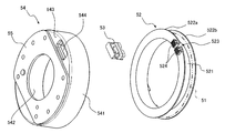
図11,12は、本発明が適用された電磁クラッチの電磁コイルユニット(フィールドコア・コイル組立)の第2実施形態を示している。図11は、第2実施形態による電磁コイルユニット50の断面図であり、図12は、電磁コイルユニット50の分解斜視図である。電磁コイルユニット50は、電磁コイル51が巻かれたボビン52と、ボビン52に取り付けられた電気コネクタ53と、ボビン52を収容する筒形状のリング体(フィールドコア)54と、を含む。
ボビン52は、外周面に電磁コイル51が巻かれる円筒部521と、円筒部521の両端部に設けられたフランジ部522a,522bと、を有する。一方のフランジ部522aの外周の一部には、切欠部523が形成されており、また、当該一方のフランジ部522aの外側面には、電気コネクタ53が装着されるコネクタ取付部524が切欠部523を挟んで設けられている。コネクタ取付部524は、フランジ部522aの外側から見て切欠部523の左側に位置する左側部分と、切欠部523の右側に位置する右側部分とを有する。
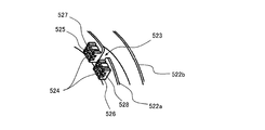
図13は、コネクタ取付部524の拡大図である。
図13に示すように、コネクタ取付部524には、導線が嵌め込まれる第1~第4溝部525~528が設けられている。第1溝部525及び第3溝部527は、コネクタ取付部524の前記左側部分に設けられ、第2溝部526及び第4溝部528は、コネクタ取付部524の前記右側部分に設けられている。
図13に示すように、コネクタ取付部524には、導線が嵌め込まれる第1~第4溝部525~528が設けられている。第1溝部525及び第3溝部527は、コネクタ取付部524の前記左側部分に設けられ、第2溝部526及び第4溝部528は、コネクタ取付部524の前記右側部分に設けられている。
本実施形態において、第1溝部525には、ボビン52(の円筒部521の外周面)に巻かれた電磁コイル51の一方の端部が嵌め込まれ、第2溝部526には、円筒部521の外周面に巻かれた電磁コイル51の他方の端部が嵌め込まれる。具体的には、ボビン52に巻かれた電磁コイル51の前記一方の端部は、切欠部523を介してフランジ部522aの外側に引き出されて第1溝部525に嵌め込まれ、ボビン52に巻かれた電磁コイル51の前記他方の端部は、切欠部523を介してフランジ部522aの外側に引き出されて第2溝部526に嵌め込まれる。また、第3溝部527には、バックサージ吸収用のダイオード(図示省略)の一方のリード線が嵌め込まれ、第4溝部528には、前記ダイオードの他方のリード線が嵌め込まれる。
図14,15は、電気コネクタ53を示している。図14は、電気コネクタ53の分解斜視図であり、図15は、電気コネクタ53の拡大断面図である。本実施形態において、電気コネクタ53は、インサート成形によって形成されており、樹脂製のハウジング531と、一対の端子部材532,532と、を有する。
ハウジング531は、底面側の所定範囲の外周面が他の部分の外周面よりも一段高く形成されている。また、ハウジング531は、一側面に形成された第1凹部531aと、底面に形成された第2凹部531bと、を有する。
端子部材532は、給電用のケーブル端子等に接続される第1接続片部533と、導線が接続される第2接続片部534と、これらを連結する連結部535と、を有する。第1接続片部533は、平板状に形成されており、ハウジング531の第1凹部531a内において、第1凹部531aの底部からハウジング531の側方に向かって突出している。第2接続片部534は、断面下向き略U字状に形成されている。第2接続片部534は、その両端部がハウジング531の第2凹部531bを形成する一対の対向壁部の内面531c,531dに固定されており(埋没しており)、前記両端部の間の中間部分が第2凹部531b内に露出している。なお、連結部535もハウジング531に埋没している。
第2凹部531b内に露出する第2接続片部534の前記中間部分には、導線が圧入される圧入スリット536,537と、導線が圧入されない非圧入スリット538,539と、が形成されている。
一方の圧入スリット536は、開口端側の幅広部536aと、奥側の幅狭部536bと、これらを接続するテーパ部536cと、を有して形成されている。幅広部536aの幅A1’は、電磁コイル51の線径よりも僅かに小さく設定され、幅狭部536bの幅A2’は、幅広部536aの幅A1’よりもさらに小さく設定されている。同様に、他方の圧入スリット537は、開口端側の幅広部537aと、奥側の幅狭部537bと、これらを接続するテーパ部537cと、を有して形成されている。幅広部537aの幅B1’は、前記ダイオードのリード線径よりも僅かに小さく設定され、幅狭部537bの幅B2’は、幅広部537aの幅B1’よりもさらに小さく設定されている。なお、電磁コイル51の線径と前記ダイオードのリード線径とが同じである場合には、A1’=B1’、A2’=B2’とすることができる。
また、第2接続片部534において、非圧入スリット538,539は、圧入スリット536,537を挟んで配置、すなわち、圧入スリット536,537よりも外側に配置されている。より具体的には、一方の非圧入スリット538は、隣接する圧入スリット536よりも隣接する対向壁部の内面531cに近い位置に形成され、他方の非圧入スリット539は、隣接する圧入スリット537よりも隣接する対向壁部の内面531dに近い位置に形成されている。
そして、電気コネクタ53は、その底面側からボビン52に設けられたコネクタ取付部524に取り付けられる。具体的には、電気コネクタ53のハウジング531の第2凹部531bがコネクタ取付部524(の外周)に嵌め込まれることにより、電気コネクタ53がボビン52に取り付けられる。電気コネクタ53がボビン52に取り付けられることにより、電気コネクタ53の一方の端子部材532が電磁コイル51の一方の端部及び前記ダイオードの一方のリード線に接続され、他方の端子部材532が電磁コイル51の他方の端部及び前記ダイオードの他方のリード線に接続される。
図11、12に戻り、リング体54は、外側筒状部541と、外側筒状部541と同心に配置された内側筒状部542と、外側筒状部541と内側筒状部542とを一端側で連結する円環板状の連結部543と、を有する。連結部543には、電気コネクタ53に対応する大きさを有した貫通孔544が形成されている。具体的には、貫通孔544は、電気コネクタ53(のハウジング531)の上面側の断面積よりも大きく、底面側の前記所定範囲の断面積よりも小さい開口面積を有している。また、連結部543の外側面には、電磁コイルユニット50を所定の場所に取り付けるための取付板55が固定されている。
リング体54は、外側筒状部541、内側筒状部542、及び連結部543で形成されるリング状の空間内に、電気コネクタ53が取り付けられたボビン52を収容する。具体的には、リング体54は、電気コネクタ53の上面側が貫通孔544を介して外部に露出した状態、すなわち、電気コネクタ53が貫通孔544に挿通された状態でボビン52を前記空間内に収容する。なお、前記空間内には、ボビン52が収容された後に樹脂材(図示省略)が充填されている。
次に、本実施形態における電磁コイルユニット50の組立手順を説明する。
まず、電磁コイル51をボビン52の円筒部521の外周面に巻き付けて固定すると共に、電磁コイル51の両端部を、ボビン52のフランジ部522aに形成された切欠部523からフランジ部522aの外側に引き出す。
まず、電磁コイル51をボビン52の円筒部521の外周面に巻き付けて固定すると共に、電磁コイル51の両端部を、ボビン52のフランジ部522aに形成された切欠部523からフランジ部522aの外側に引き出す。
次いで、電磁コイル51の一方の端部を、コネクタ取付部524の前記左側部分に設けられた第1溝部525に嵌め込み、電磁コイル51の他方の端部を、コネクタ取付部524の前記右側部分に設けられた第2溝部526に嵌め込む。このとき、電磁コイル51の両端部は、互いに逆向きに曲げられることになる。また、前記ダイオードの一方のリード線を、コネクタ取付部524の左側部分に設けられた第3溝部527に嵌め込み、前記ダイオードの他方のリード線を、コネクタ取付部524の前記右側部分に設けられた第4溝部528に嵌め込む。
次いで、図16に示すように、電気コネクタ53をボビン52のフランジ部522aの外側面に設けられたコネクタ取付部524の上部にセットする。このとき、第2接続片部534に形成された一方の圧入スリット536は、コネクタ取付部524の第1溝部525に嵌め込まれた電磁コイル51の一方の端部51a又はコネクタ取付部524の第2溝部526に嵌め込まれた電磁コイル51の他方の端部51b上に配置され、他方の圧入スリット537は、コネクタ取付部524の第3溝部527に嵌め込まれた前記ダイオードの一方のリード線La又はコネクタ取付部524の第4溝部528に嵌め込まれた他方のリード線Lb上に配置される。
次いで、コネクタ取付部524にセットされた電気コネクタ53を、ボビン52のフランジ部522aに向かって押し下げる。すると、図17に示すように、電気コネクタ53のハウジング531の底面に形成された第2凹部531bが、コネクタ取付部524の外周面に嵌合されて取り付けられる。このとき、第2接続片部534に形成された一方の圧入スリット536の幅狭部536bに電磁コイル51の端部51a(51b)が圧入され、他方の圧入スリット537の幅狭部537bに前記ダイオードのリード線La(Lb)が圧入される。これにより、電気コネクタ53の一方の端子部材532の第2接続片部534が、電磁コイル51の一方の端部51a及び前記ダイオードの一方のリード線Laに接続され、他方の端子部材532の第2接続片部534が、電磁コイル51の他方の端部51b及び前記ダイオードの他方のリード線Lbに接続される。ここで、図17に示すように、非圧入スリット538,539の深さ(長さ)Mは、導線(電磁コイル51の端部51a,51b、前記ダイオードのリード線La,Lb)の圧入スリット536,537への圧入深さN、すなわち、圧入スリット536,537に圧入された導線の圧入スリット536,537の開口端からの距離よりも大きく設定されている。
次いで、電気コネクタ53が取り付けられたボビン52を、リング体54の前記空間内に収容する。このとき、電気コネクタ53が、リング体54の連結部543に形成された貫通孔544に挿通される。
ここで、上述したように、貫通孔544の開口面積は、電気コネクタ53の底面側の前記所定範囲の断面積よりも小さい。換言すれば、図18に示すように、電気コネクタ53のハウジング531の第2凹部531bを形成する一対の対向壁部の外面531e,531f間の幅寸法Oは、リング体54の連結部543に形成された貫通孔544の対応する内寸(内壁間の距離)Pよりも大きく設定されている。また、電気コネクタ53の端子部材532の第2接続片部534において、非圧入スリット538の幅E’と非圧入スリット539の幅F’の合算値(E’+F’)は、電気コネクタ53のハウジング531の幅寸法Oから貫通孔544の対応する内寸Pを引いた値(O-P)以上に設定されている。
その後、リング体54の外側筒状部541、内側筒状部542、及び連結部543によって形成される前記空間内に樹脂材を充填し、電磁コイル51を封止すると共に電磁コイル51、ボビン52、電気コネクタ53、及びリング体54を一体化する。これにより、電磁コイルユニット50の組立が完成する。
上述の構成によれば、電気コネクタ53をボビン52のコネクタ取付部524に取り付けることにより、電気コネクタ53の端子部材532の第2接続片部534に形成された圧入スリット536,537(具体的には、幅狭部536b,537b)に、電磁コイル51の端部51a,51b及び前記ダイオードのリード線La,Lbが圧入される。このため、電気コネクタ53と、電磁コイル51及び前記ダイオードとを容易かつ確実に接続することができる。
また、電気コネクタ53のハウジング531の幅寸法Oが、リング体54の連結部543に形成された貫通孔544の対応する内寸Pよりも大きく設定されており、電気コネクタ53は貫通孔544に圧入されることとなる。このため、電気コネクタ53がリング体54にがたつきなく保持され、また、リング体54の前記空間内に樹脂材を充填する際に、貫通孔544から樹脂材が漏れ出ることもない。
ここで、電気コネクタ53の端子部材532の第2接続片部534には、圧入スリット536,537に加えて、これらを挟んで非圧入スリット538,539が形成されている。このため、電気コネクタ53を貫通孔544に挿通させる(圧入する)際に、電気コネクタ53のハウジング531が貫通孔544の内壁から受ける力によって生じる端子部材532の第2接続片部534の変形が、非圧入スリット538,539によって吸収される。これにより、圧入スリット536,537の幅が狭まってしまうことが抑制され、電磁コイル51の端部51a,51bや前記ダイオードのリード線La,Lbを必要以上に傷つけたり、断線させたりするおそれが大幅に低減される。したがって、本実施形態において、非圧入スリット538,539が本発明の「抑制部」に相当する。
特に、本実施形態においては、非圧入スリット528の幅E’と非圧入スリット529の幅F’の合算値(E’+F’)が、電気コネクタ53のハウジング531の幅寸法Oから貫通孔544の対応する内寸Pを引いた値(O-P)以上に設定されている。このため、電磁コイル51の端部51a,52bや前記ダイオードのリード線La,Lbを必要以上に傷つけたり、断線させたりすることがより確実に防止される。
なお、本実施形態において、第2接続片部534は、二つの圧入スリット536,537を挟むように配置された二つの非圧入スリット538,539を有している。しかし、これに限るものではなく、第2接続片部534は、第1実施形態における接続片部23と同様に、非圧入スリット538,539の一方だけを有するように構成されてもよい。この場合、当該非圧入スリットの幅は、電気コネクタ53のハウジング531の幅寸法Oから貫通孔544の対応する内寸Pを引いた値(O-P)以上に設定されるのが好ましい。また、本実施形態において、第2接続片部534は、二つの圧入スリット536,537を有しているが、第2接続片部534が有する圧入スリットの個数は、一つであってもよいし、三つ以上であってもよい。
さらに、第2接続片部534は、図19に示すように、非圧入スリット538,539に代えて、切欠き部61,62を有してもよい。切欠き部61,62は、圧入スリット536,537の側方において、第2接続片部534と、電気コネクタ53のハウジング531の第2凹部531bを形成する一対の対向壁部の内面531c,531dとの間に所定幅の隙間g1,g2を形成する。この場合、好ましくは、隙間g1の幅Qと隙間g2の幅Rとの合算値(Q+R)は、電気コネクタ53のハウジング531の幅寸法Oから貫通孔544の対応する内寸Pを引いた値(O-P)以上に設定され、隙間g1,g2の長さ(長手方向の寸法)Sは、導線の圧入スリット536,537への圧入深さNよりも大きく設定される。なお、Q=Rとすることができる。さらに、第2接続片部534は、隙間g1,g2のいずれか一方のみを形成する切欠き部を有して構成されてもよく、この場合には、当該隙間の幅が(O-P)以上に設定されるのが好ましい。
以上、本発明の好ましい実施形態について説明したが、本発明は上記実施形態に制限されるものではなく、本発明の技術的思想に基づいて種々の変形及び変更が可能である。
1…電磁コイルユニット、2…電磁コイル、2a,2b…電磁コイルの端部(導線)、3…リング体、10…ケース、11…凹状の取付部、21…端子部材、23…接続片部、23a,23b…接続片部の側縁部、24,25…圧入スリット(第1スリット)、27,27…非圧入スリット(第2スリット)、28,29…切欠き部、30…ダイオード、30a,30b…ダイオードのリード線(導線)、50…電磁コイルユニット、51…電磁コイル、51a,51b…電磁コイルの端部(導線)、52…ボビン、53…電気コネクタ、54…リング体、61,62…切欠き部、524…コネクタ取付部、531…電気コネクタのハウジング、531a…第1凹部、531b…第2凹部、531c,531d…対向壁部の内面、531e,531f…対向壁部の外面、532…端子部材、533…第1接続片部、534…第2接続片部、536,537…圧入スリット(第1スリット)、538,539…非圧入スリット(第2スリット)、544…貫通孔(挿通孔)、La,Lb…ダイオードのリード線(導線)
Claims (9)
- 導線が圧入される少なくとも一つの第1スリットが形成された接続片部を有すると共に当該接続片部が凹状の取付部内に装着される端子部材であって、
前記少なくとも一つの第1スリットを挟む前記接続片部の両側縁部間の幅寸法は、前記取付部の対応する内寸よりも大きく設定され、
前記接続片部には、前記接続片部が前記取付部内に装着される際に前記少なくとも一つの第1スリットの幅が狭まることを抑制する抑制部が形成されている、端子部材。 - 前記接続片部には、前記抑制部として、前記少なくとも一つの第1スリットよりも前記両側縁部の少なくとも一方に近い前記接続片部の部位に導線が圧入されない第2スリットが形成されており、
前記第2スリットの幅の合算値が、前記接続片部の前記両側縁部間の幅寸法から前記取付部の対応する内寸を引いた値以上に設定されている、請求項1に記載の端子部材。 - 前記第2スリットは、隣接する第1スリットよりも隣接する側縁部に近い位置に形成されている、請求項2に記載の端子部材。
- 前記取付部内の所定位置に前記導線が配置された後に前記接続片部が前記取付部内に嵌装着される、請求項1~3のいずれか一つに記載の端子部材。
- 凹部を有する樹脂製のハウジングと、
導線が圧入される少なくとも一つの第1スリットが形成された接続片部を有すると共に前記少なくとも一つの第1スリットを挟む前記接続片部の両端が前記ハウジングの前記凹部を形成する一対の対向壁部に固定された端子部材と、
を有し、前記ハウジングが所定の挿通孔に挿通される電気コネクタであって、
前記ハウジングの前記一対の対向壁部の外面間寸法は、前記挿通孔の対応する内寸よりも大きく設定され、
前記接続片部には、前記ハウジングが前記挿通孔に挿通される際に前記少なくとも一つの第1スリットの幅が狭まることを抑制する抑制部が形成されている、電気コネクタ。 - 前記接続片部には、前記抑制部として、前記少なくとも一つの第1スリットよりも前記ハウジングの前記一対の対向壁部の少なくとも一方の内面に近い前記接続片部の部位に導線が圧入されない第2スリットが形成されており、
前記第2スリットの幅の合算値が、前記ハウジングの前記一対の対向壁部の外面間寸法から前記取付部の対応する内寸を引いた値以上に設定されている、請求項5に記載の電気コネクタ。 - 前記第2スリットは、隣接する第1スリットよりも隣接する前記対向壁部の内面に近い位置に形成されている、請求項6に記載の電気コネクタ。
- 前記少なくとも一つの第1スリットに導線が圧入された後に前記ハウジングが前記挿通孔に挿通される、請求項5~7のいずれか一つに記載の電気コネクタ。
- 請求項1~4のいずれか一つに記載の端子部材、又は、請求項5~8のいずれか一つに記載の電気コネクタを含む車両用圧縮機の電磁クラッチ。
Applications Claiming Priority (2)
| Application Number | Priority Date | Filing Date | Title |
|---|---|---|---|
| JP2014-140844 | 2014-07-08 | ||
| JP2014140844A JP2016018676A (ja) | 2014-07-08 | 2014-07-08 | 端子部材、電気コネクタ、及び電磁クラッチ |
Publications (1)
| Publication Number | Publication Date |
|---|---|
| WO2016006277A1 true WO2016006277A1 (ja) | 2016-01-14 |
Family
ID=55063923
Family Applications (1)
| Application Number | Title | Priority Date | Filing Date |
|---|---|---|---|
| PCT/JP2015/057791 Ceased WO2016006277A1 (ja) | 2014-07-08 | 2015-03-17 | 端子部材、電気コネクタ、及び電磁クラッチ |
Country Status (2)
| Country | Link |
|---|---|
| JP (1) | JP2016018676A (ja) |
| WO (1) | WO2016006277A1 (ja) |
Families Citing this family (1)
| Publication number | Priority date | Publication date | Assignee | Title |
|---|---|---|---|---|
| KR102349151B1 (ko) * | 2020-03-24 | 2022-01-11 | 두원중공업(주) | 전동압축기의 모터용 커넥터 |
Citations (3)
| Publication number | Priority date | Publication date | Assignee | Title |
|---|---|---|---|---|
| JP2000266083A (ja) * | 1999-03-18 | 2000-09-26 | Sanden Corp | 導線接続用端子部材 |
| JP3346521B2 (ja) * | 1995-07-26 | 2002-11-18 | 住友電装株式会社 | 圧接コネクタ |
| JP4157383B2 (ja) * | 2001-04-25 | 2008-10-01 | ミラコ インコーポレイテッド | フラットフレキシブルケーブルコネクタの使用方法及び装置 |
-
2014
- 2014-07-08 JP JP2014140844A patent/JP2016018676A/ja active Pending
-
2015
- 2015-03-17 WO PCT/JP2015/057791 patent/WO2016006277A1/ja not_active Ceased
Patent Citations (3)
| Publication number | Priority date | Publication date | Assignee | Title |
|---|---|---|---|---|
| JP3346521B2 (ja) * | 1995-07-26 | 2002-11-18 | 住友電装株式会社 | 圧接コネクタ |
| JP2000266083A (ja) * | 1999-03-18 | 2000-09-26 | Sanden Corp | 導線接続用端子部材 |
| JP4157383B2 (ja) * | 2001-04-25 | 2008-10-01 | ミラコ インコーポレイテッド | フラットフレキシブルケーブルコネクタの使用方法及び装置 |
Also Published As
| Publication number | Publication date |
|---|---|
| JP2016018676A (ja) | 2016-02-01 |
Similar Documents
| Publication | Publication Date | Title |
|---|---|---|
| US5812044A (en) | Electromagnetic clutch | |
| KR101659298B1 (ko) | 내부 쉴딩 배열을 가진 동축 커넥터 및 이를 조립하는 방법 | |
| US9277658B2 (en) | Electronic controller and method of manufacturing the electronic controller | |
| US11508499B2 (en) | Grommet with groove portion between pair of contact portions, and wire harness | |
| JP5951110B2 (ja) | 電動機の固定子、電動機、空気調和機、及び電動機の固定子の製造方法 | |
| US10236634B2 (en) | Electromagnetic shield member and electromagnetic shield member-equipped wiring device | |
| JP6691072B2 (ja) | コネクタ | |
| JP5600034B2 (ja) | 電磁連結装置 | |
| JP6291463B2 (ja) | ノイズフィルタ及びワイヤハーネス | |
| US9592775B2 (en) | Wiring harness protector fixing structure | |
| CN103403975A (zh) | 具有小壳体的连接器 | |
| US11153689B2 (en) | Loudspeaker and method of manufacturing loudspeaker | |
| US10411387B2 (en) | Terminal | |
| EP3974261A1 (en) | Grommet and wire harness | |
| JPWO2015166571A1 (ja) | 車両用制御装置 | |
| CN111902890B (zh) | 线束 | |
| US20160053829A1 (en) | Electromagnetic Clutch | |
| JP2016018676A (ja) | 端子部材、電気コネクタ、及び電磁クラッチ | |
| US10431938B2 (en) | Shield shell and shield connector | |
| CN111210984A (zh) | 点火线圈单元 | |
| CN106329840A (zh) | Dc电动机 | |
| CN114006201B (zh) | 连接器 | |
| JP4783042B2 (ja) | シールド固定部 | |
| WO2024162033A1 (ja) | コネクタおよびワイヤハーネス | |
| JP2020056362A (ja) | 内燃機関用点火コイル |
Legal Events
| Date | Code | Title | Description |
|---|---|---|---|
| 121 | Ep: the epo has been informed by wipo that ep was designated in this application |
Ref document number: 15818166 Country of ref document: EP Kind code of ref document: A1 |
|
| NENP | Non-entry into the national phase |
Ref country code: DE |
|
| 122 | Ep: pct application non-entry in european phase |
Ref document number: 15818166 Country of ref document: EP Kind code of ref document: A1 |