WO2015199210A1 - チップオン基板及びそれを用いた電子装置の製造方法 - Google Patents
チップオン基板及びそれを用いた電子装置の製造方法 Download PDFInfo
- Publication number
- WO2015199210A1 WO2015199210A1 PCT/JP2015/068484 JP2015068484W WO2015199210A1 WO 2015199210 A1 WO2015199210 A1 WO 2015199210A1 JP 2015068484 W JP2015068484 W JP 2015068484W WO 2015199210 A1 WO2015199210 A1 WO 2015199210A1
- Authority
- WO
- WIPO (PCT)
- Prior art keywords
- substrate
- chip
- resin
- mass
- parts
- Prior art date
- Legal status (The legal status is an assumption and is not a legal conclusion. Google has not performed a legal analysis and makes no representation as to the accuracy of the status listed.)
- Ceased
Links
Images

Classifications
-
- B—PERFORMING OPERATIONS; TRANSPORTING
- B32—LAYERED PRODUCTS
- B32B—LAYERED PRODUCTS, i.e. PRODUCTS BUILT-UP OF STRATA OF FLAT OR NON-FLAT, e.g. CELLULAR OR HONEYCOMB, FORM
- B32B15/00—Layered products comprising a layer of metal
- B32B15/04—Layered products comprising a layer of metal comprising metal as the main or only constituent of a layer, which is next to another layer of the same or of a different material
- B32B15/08—Layered products comprising a layer of metal comprising metal as the main or only constituent of a layer, which is next to another layer of the same or of a different material of synthetic resin
-
- B—PERFORMING OPERATIONS; TRANSPORTING
- B32—LAYERED PRODUCTS
- B32B—LAYERED PRODUCTS, i.e. PRODUCTS BUILT-UP OF STRATA OF FLAT OR NON-FLAT, e.g. CELLULAR OR HONEYCOMB, FORM
- B32B15/00—Layered products comprising a layer of metal
- B32B15/04—Layered products comprising a layer of metal comprising metal as the main or only constituent of a layer, which is next to another layer of the same or of a different material
- B32B15/08—Layered products comprising a layer of metal comprising metal as the main or only constituent of a layer, which is next to another layer of the same or of a different material of synthetic resin
- B32B15/09—Layered products comprising a layer of metal comprising metal as the main or only constituent of a layer, which is next to another layer of the same or of a different material of synthetic resin comprising polyesters
-
- H—ELECTRICITY
- H10—SEMICONDUCTOR DEVICES; ELECTRIC SOLID-STATE DEVICES NOT OTHERWISE PROVIDED FOR
- H10W—GENERIC PACKAGES, INTERCONNECTIONS, CONNECTORS OR OTHER CONSTRUCTIONAL DETAILS OF DEVICES COVERED BY CLASS H10
- H10W70/00—Package substrates; Interposers; Redistribution layers [RDL]
- H10W70/60—Insulating or insulated package substrates; Interposers; Redistribution layers
-
- H—ELECTRICITY
- H10—SEMICONDUCTOR DEVICES; ELECTRIC SOLID-STATE DEVICES NOT OTHERWISE PROVIDED FOR
- H10W—GENERIC PACKAGES, INTERCONNECTIONS, CONNECTORS OR OTHER CONSTRUCTIONAL DETAILS OF DEVICES COVERED BY CLASS H10
- H10W70/00—Package substrates; Interposers; Redistribution layers [RDL]
- H10W70/60—Insulating or insulated package substrates; Interposers; Redistribution layers
- H10W70/67—Insulating or insulated package substrates; Interposers; Redistribution layers characterised by their insulating layers or insulating parts
- H10W70/69—Insulating materials thereof
Definitions
- the present invention relates to a chip-on-substrate and an electronic device manufacturing method using the chip-on-substrate.
- COF Chip on Film
- PI polyimide
- the COF substrate has an insulating protective film (resist film) 15 made of a thermosetting resin in addition to the basic configuration described above, and a part of the film substrate 11 and the metal wiring portion 13. (Refer to patent document 2).
- the COF substrate 1 of the present invention has the insulating protective film 15 as an essential constituent element.
- the migration resistance of the COF substrate can be remarkably improved.
- the insulating protective film 15 also functions as a reflector for incident light, and the brightness of the LED light emitting device can be improved.
- the COF substrate 1 having an insulating protective film has excellent migration resistance as described above.
- material selection must be restricted due to the presence of the insulating protective film. That is, since the heating temperature for the thermosetting treatment necessary for forming an insulating protective film made of a thermosetting resin such as polyester resin is generally 80 ° C. or higher, a COF substrate such as a base film is formed.
- the material selection of other members is a restriction that the material is limited to a material that can withstand the heating at the above-mentioned temperature at the time of manufacture.
- the polyester-based resin that forms the insulating protective film 15 is mainly ignited starting from the organic component of the solder.
- the problem that the member may be damaged by heat has also been a problem to be solved.
- the present invention has been made in view of the above situation, and in the case where the COF substrate is configured to include the insulating protective film 15 that improves the migration resistance characteristics, the film substrate that constitutes the COF substrate is provided. It is an object of the present invention to provide a high-quality COF substrate at a lower cost by avoiding restrictions on material selection.
- the inventors of the present invention applied a heat resistance improving treatment such as annealing to the thermoplastic resin forming the film substrate of the COF substrate, and the heat shrinkage of the thermoplastic resin. Pretreatment is performed so that the starting temperature is equal to or higher than the thermosetting temperature of the thermosetting ink for forming the insulating protective film, or a predetermined amount of the inorganic ink is used to form the insulating protective film for the COF substrate. It has been found that the above-mentioned problems can be solved by including a white pigment and an inorganic flame retardant, and the present invention has been completed. Specifically, the present invention provides the following.
- a chip-on substrate on which an electronic device can be mounted and is formed so as to cover a film substrate, a metal wiring part formed on the film substrate, and a part of the film substrate and the metal wiring part.
- thermoplastic resin is polyethylene naphthalate
- thermal contraction start temperature of the polyethylene naphthalate is 100 ° C. or higher.
- the insulating protective film is formed of a thermosetting ink having a polyester resin as a base resin, and the thermosetting temperature of the polyester resin is 100 ° C. or lower (1) or (2) The chip-on-substrate described in 1.
- the insulating protective film uses a thermosetting resin as a base resin, an inorganic white pigment of 200 to 600 parts by mass with respect to 100 parts by mass of the base resin, and 100 parts by mass of the base resin
- thermosetting resin is an epoxy resin.
- the flame retardant is aluminum hydroxide or a phosphorus-based flame retardant, and the content with respect to 100 parts by mass of the base resin is 25 parts by mass or more and 200 parts by mass or less.
- the COF substrate when configured to include the insulating protective film 15 that improves the migration resistance, it is possible to avoid the selection of the material of the film substrate that constitutes the COF substrate and to improve the quality at a lower cost.
- a COF substrate can be provided.
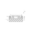
- FIG. 2 is a cross-sectional view schematically showing a layer configuration of a COF substrate in the AA cross section of FIG. 1.
- COF board A COF substrate 1, which is a preferred embodiment of the present invention, will be described with reference to FIGS. As shown in FIGS. 1 and 2, the COF substrate 1 has a conductive metal wiring portion 13 made of metal foil on an adhesive layer 12 on the surface of a flexible film substrate 11 made of a thermoplastic resin. Is formed. An insulating protective film 15 made of thermosetting ink is formed so as to cover a part of the film substrate 11 and the metal wiring part 13.
- the insulating protective film 15 is formed on almost the entire surface of the surface of the metal wiring portion 13 except for the portion to be connected to the electronic device 2 and on the surface of the film substrate 11 Of these, the metal wiring portion 13 is formed so as to cover almost the entire non-formed portion.
- the COF substrate 1 having the above configuration is used in a state where the electronic device 2 such as an LED light emitting device is mounted on the metal wiring portion 13 in a conductive manner via the solder layer 14.
- the film substrate 11 a thermoplastic resin formed into a sheet shape can be used.
- the sheet form is a concept including a film form, and there is no difference between the two in the present invention as long as both are flexible.
- the thermoplastic resin is also required to have a high insulating property.
- the thickness of the film substrate 11 is not particularly limited, but is preferably about 50 ⁇ m or more and 100 ⁇ m or less from the viewpoint of heat resistance and insulation properties and a balance between manufacturing costs. Also, the thickness is preferably within the above-mentioned thickness range from the viewpoint of maintaining good productivity when manufacturing by the roll-to-roll method.
- any resin having a volume resistivity that can provide the insulation required for the COF substrate 1 at the time of integration as an electronic device may be used.
- the volume resistivity of the film substrate 11 is preferably 10 14 ⁇ ⁇ cm or more, and more preferably 10 18 ⁇ ⁇ cm or more.
- polyimide resin excellent in heat resistance, dimensional stability during heating, mechanical strength, and durability
- various general-purpose thermoplastic resins whose heat resistance and dimensional stability are improved to a predetermined value or higher by performing a heat resistance improving process such as an annealing process can be used.
- Specific examples of such a general-purpose thermoplastic resin include polyethylene naphthalate (PEN).
- PEN can provide necessary and sufficient heat resistance and dimensional stability by annealing, and is clearly superior to PI in transparency and economy.
- the use of PEN as a film substrate has been problematic in that it has low flame retardancy compared to PI.
- the flame retardancy should be sufficiently improved as the entire layer structure of the COF substrate. Therefore, these resins can be selected without any problem as a material resin for the film substrate.
- the COF substrate 1 of the present invention has the insulative protective film 15 made of a thermosetting resin such as thermosetting ink as an essential constituent element as described above. Therefore, the heat resistance of the thermoplastic resin forming the film substrate 11 is improved by the annealing treatment so that the thermal shrinkage starting temperature is equal to or higher than the thermosetting temperature of the thermosetting resin forming the insulating protective film 15.
- the thermosetting resin forming the insulating protective film 15 is a polyester-based thermosetting resin and the thermosetting temperature is about 80 ° C.
- the thermal shrinkage of PEN which is usually about 80 ° C.
- the starting temperature may be increased to about 100 ° C. by annealing. Thereby, it is possible to form the insulating protective film 15 having sufficient heat resistance, strength and insulation while avoiding minute heat damage of the film substrate 11. Details of a specific implementation method of the annealing process will be described later.
- thermal shrinkage start temperature means that a sample sheet made of a thermoplastic resin to be measured is set in a TMA apparatus, a load of 1 g is applied, and the temperature is increased to 120 ° C. at a temperature rising rate of 2 ° C./min. Measure the amount of shrinkage (in%) at that time, output this data and record the temperature and amount of shrinkage, read the temperature that deviates from the 0% baseline due to shrinkage, and heat shrink the temperature This is the starting temperature.
- thermosetting temperature in the present specification is the measurement and calculation of the temperature at the rising position of the thermosetting reaction when the thermosetting resin to be measured is heated, and that temperature is the thermosetting temperature.
- the “heat resistance improving process” in the present specification an annealing process which is the most general processing method can be adopted as the heat resistance improving process for improving the dimensional stability during heating.
- the “heat resistance improving process” constituting the present invention is not limited to this, and includes a general processing process for improving the above-described thermal shrinkage start temperature of the thermoplastic resin as compared with the state before the process.
- the heat resistance improving process is an annealing process will be described as a representative embodiment of the present invention.
- the metal wiring part 13 is preferably joined to the surface of the COF substrate 1 by a dry laminating method with the adhesive layer 12 interposed.
- the adhesive for forming the adhesive layer 12 a known resin-based adhesive may be appropriately used as long as it has heat resistance at the thermosetting temperature of the thermosetting resin for forming the insulating protective film 15 described above. it can. Of these resin adhesives, urethane, polycarbonate, or epoxy adhesives can be preferably used.
- the metal wiring portion 13 is a wiring pattern made of a conductive base material formed on the surface of the COF substrate 1.
- the metal wiring part 13 has a function of supplying electricity by causing a necessary current to flow between the plurality of electronic devices 2.
- the metal wiring portion 13 is formed on the surface of the film substrate 11 as a complicated wiring pattern in which a plurality of fine comb-shaped metal wirings are arranged close to each other without intersecting or contacting each other.
- the thickness of the metal wiring portion 13 may be set as appropriate according to the magnitude of the withstand current required for the COF substrate 1 and is not particularly limited, and examples thereof include a thickness of 10 ⁇ m to 50 ⁇ m.
- Examples of the conductive base material for forming the metal wiring portion 13 include metals and metal compounds, and it is essential that these materials can be etched. A method for forming the pattern of the metal wiring portion by etching will be described later.
- Examples of the metal or metal compound include metals such as copper, aluminum, nickel, iron, gold, silver, indium, antimony, tin, and zinc, and metals such as oxides, nitrides, sulfides, and carbides of the above metals. Compounds.
- examples of the material constituting the metal wiring portion 13 include composite materials of the above metals and the above metal compounds (for example, indium tin oxide (ITO), antimony tin oxide (ATO), etc.). Among them, in the production method of the present invention, a copper foil that is excellent in conductivity and workability and is easily available can be used particularly preferably.
- the metal wiring portion 13 needs to have high conductivity, and the surface resistance value is preferably 500 ⁇ / ⁇ or less, more preferably 300 ⁇ / ⁇ or less, further preferably 100 ⁇ / ⁇ or less, particularly 50 ⁇ / ⁇ or less. preferable.
- the lower limit is about 0.005 ⁇ / ⁇ .
- solder layer In the COF substrate 1, the metal wiring part 13 and the electronic device 2 are joined through the solder layer 14. Details of the soldering method will be described later, but can be roughly classified into either a reflow method or a laser method. Among these, in particular, in the laser system, since the heat exceeding the ignition point temperature is instantaneously applied to the resin, the risk of ignition increases. When the COF substrate 1 uses PEN having a higher transparency than PI that has been widely used for the film substrate 11 in the past, laser bonding can be performed in a more preferable manner.
- the solder for forming the solder layer 14 is a high-melting-point solder having a melting point of 217 ° C. or higher, preferably about 230 ° C. and containing tin, silver, and copper (“Sn—Ag” in this specification). Also referred to as “-Cu solder” can be preferably used.
- This solder has a melting point of about 150 ° C., which has been widely used, and is superior in strength and durability after solidification to a so-called Sn—Bi type low melting point solder containing tin and bismuth.
- the COF substrate 1 can sufficiently increase the limit of the heatable temperature during the soldering process by using the film substrate 11 whose heat resistance is improved by the annealing process. Therefore, the above-mentioned high melting point solder can be selected.
- the thermal damage of the base material by the high melting point solder can be avoided more reliably by performing the joining by soldering by the laser method.
- a high melting point solder (trade name “TLF-204-NH” manufactured by Tamura Seisakusho Co., Ltd.) having a melting point of 5: 3.0: 0.5 and 216 ° C. can be mentioned.
- the melting point is 150 ° C. or higher, preferably 210 ° C. or higher. It is possible to fully enjoy the effects peculiar to the present application that cannot be obtained by so-called low-temperature soldering at about ° C.
- the insulating protective film 15 is made of a material made of a thermosetting resin, preferably a thermosetting ink, except for a portion that requires electrical bonding on the surface of the metal wiring portion 13 and the film substrate 11. In other parts, it is formed mainly for improving the migration resistance of the COF substrate 1.
- the thermosetting ink has a heat curing temperature of about 100 ° C. or less.
- the known ink can be suitably used as appropriate.
- an ink that can preferably use an insulating ink having a polyester resin, an epoxy resin, an epoxy resin and a phenol resin, an epoxy acrylate resin, a silicone resin, or the like as a base resin, respectively.
- polyester-based thermosetting insulating ink is particularly preferable as a material for forming the insulating protective film 15 of the COF substrate 1 because of its excellent flexibility.
- the insulating protective film 15 is formed of white ink having flame retardancy using a thermosetting resin as a base resin.
- This white ink has an inorganic white pigment of 200 to 600 parts by mass with respect to 100 parts by mass of the base resin, and an inorganic difficulty of 25 to 200 parts by mass with respect to 100 parts by mass of the base resin.
- a flame retardant e.g., the non-flammable white pigment is originally added for the purpose of improving the design and / or light reflectivity of the COF substrate 1, while exhibiting such effects. At the same time, due to its nonflammability, there is also an effect of further enhancing the flame retardancy improving effect of the inorganic flame retardant.
- the insulating protective film 15 is whitened, so that it is possible to naturally enjoy the improvement of the design and the improvement of the lighting performance when the COF substrate 1 constitutes the lighting device. .
- thermosetting resin used as the base resin of the white ink having flame retardancy is preferably an epoxy resin having excellent flame retardancy.
- the thermal contraction start temperature of PEN used for the film substrate 11 can be improved to about 100 ° C. by annealing. It is also possible to adopt PI having more excellent heat resistance.
- the thermoplastic resin used for the film substrate 11 has a thermosetting temperature of about 100 ° C. or less, a known thermosetting ink can be suitably used.
- this epoxy thermosetting insulating ink is preferable as a material for forming the insulating protective film 15 of the COF substrate 1 from the viewpoint of excellent heat resistance.
- the inorganic white pigment is preferably titanium dioxide.
- the inorganic flame retardant is preferably aluminum hydroxide or a phosphorus flame retardant.
- the base resin of the flame retardant white ink is an epoxy resin
- the inorganic white pigment is titanium dioxide
- the inorganic flame retardant is phosphorus
- the base resin Content of the titanium dioxide with respect to 100 mass parts is 200 mass parts or more and 600 mass parts or less, Preferably, they are 400 mass parts or more and 500 mass parts or less.
- the same content of the phosphorus-based flame retardant is 25 parts by mass or more and 200 parts by mass or less, and preferably 100 parts by mass or more and 150 parts by mass or less.
- the insulating protective film 15 By forming the insulating protective film 15 with the flame-retardant white ink having such a composition, the damage caused by the fire of the COF substrate when the electronic device 2 is joined to the COF substrate 1 by soldering is sufficiently suppressed. Can do.
- formation of the insulating protective film 15 with the above insulating thermosetting ink can be performed by well-known methods, such as screen printing.
- the electronic device 2 is not particularly limited, but when the insulating protective film 15 is a white layer, an electronic device equipped with an LED light emitting element can be cited as a specific example of a particularly preferred embodiment of the COF substrate 1.
- ⁇ Method for producing COF substrate> The COF substrate 1 can be manufactured by an etching process which is one of conventionally known methods for manufacturing an electronic substrate. In addition, when the annealing process is performed on the resin base material in advance, the degree of freedom in resin selection is increased. In other respects, the conventional manufacturing method can be preferably applied.
- the annealing process can use a conventionally known heat treatment means, and is not limited to a specific heat treatment method. For example, it can also be based on a method of stacking peelable support equipment.
- the annealing treatment temperature when the thermoplastic resin forming the film substrate 11 is PEN, the glass transition temperature to the melting point range, specifically 160 ° C. to 260 ° C., more preferably 180 ° C. to 230 ° C. It is in the range of ° C.
- An example of the annealing time is about 10 seconds to 5 minutes. According to such heat treatment conditions, the thermal contraction start temperature of PEN, which is generally about 80 ° C., can be improved to about 100 ° C.
- this annealing process may be performed in-line continuously with the subsequent etching process, but productivity can be further improved by performing the process separately off-line separately from the same process.
- a metal foil such as a copper foil that is the material of the metal wiring portion 13 is laminated to obtain a laminate that is the material of the COF substrate 1.
- a metal foil is adhered to the surface of the film substrate 11 with an adhesive, or a plating method or a vapor deposition method (sputtering, ion plating, electron beam evaporation, Examples thereof include a method of depositing a metal foil by vacuum deposition, chemical vapor deposition, or the like.
- a method of bonding a metal foil to the surface of the film substrate 11 with a urethane-based adhesive is advantageous.
- an etching mask patterned in the shape of the metal wiring portion 13 is formed on the surface of the metal foil of the above laminate.
- the etching mask is provided so that the wiring pattern forming portion of the metal foil that will become the metal wiring portion 13 is free from corrosion by the etching solution.
- the method for forming the etching mask is not particularly limited.
- the etching mask may be formed on the surface of the laminated sheet by exposing the photoresist or dry film through the photomask and then developing the ink mask.
- An etching mask may be formed on the surface of the laminated sheet by this printing technique.
- the metal foil in a portion not covered with the etching mask is removed with an immersion liquid. Thereby, parts other than the location used as the metal wiring part 13 are removed among metal foil.
- the etching mask is removed using an alkaline stripping solution.
- the etching mask is removed from the surface of the metal wiring portion 13.
- the COF substrate 1 is completed.
- a plurality of formation regions of the metal wiring portion 13 including a desired wiring pattern are arranged in a grid pattern on a wide resin sheet for forming the film substrate 11.
- the installed COF material is used. And it is common to cut
- the position in the width direction of the sheet is determined by an edge position controller (EPC) that recognizes the sheet edge.
- EPC edge position controller
- the insulating protective film 15 can be formed by a known method such as screen printing as described above.
- the COF substrate 1 described above can be used as the electronic device 10 by bonding the electronic device 2 such as an LED light emitting device to the metal wiring portion 13 so as to be conductive.
- the joining of the electronic device 2 to the metal wiring portion 13 can be suitably performed by soldering.
- This solder bonding can be performed by a reflow method or a laser method.
- the electronic device 2 is mounted on the metal wiring part 13 via solder, and then the COF substrate 1 is transported into the reflow furnace, and hot air at a predetermined temperature is blown to the metal wiring part 13 in the reflow furnace.
- the solder paste is melted and the electronic device 2 is soldered to the metal wiring portion 13.
- the laser method is a technique in which solder is locally heated by a laser to solder the electronic device 2 to the metal wiring portion 13.
- the COF substrate 1 can exhibit superiority in terms of productivity, particularly in the case of a manufacturing method using a laser.
- the combination of the COF substrate 1 and the above method is an electronic It is possible to make a special contribution to improving the productivity of the device.
- the COF substrate 1 is subjected to a heat treatment such as an annealing treatment on the thermoplastic resin forming the film substrate 11 in advance, so that the thermal shrinkage start temperature is equal to or higher than the thermosetting temperature of the insulating protective film 15. It is a thing. Thereby, the freedom degree in the material selection of the film board
- the film substrate 11 is excellent in heat resistance and mechanical strength, but instead of PI, which is inferior in transparency and extremely expensive, by increasing the heat shrinkage starting temperature to 100 ° C. or higher by annealing, PEN Now available.
- the annealed PEN has sufficient heat resistance, and is superior to PI in transparency. Nevertheless, in terms of economy, it is much cheaper than PI. Therefore, it is possible to stably provide the COF substrate 1 having a sufficiently high quality while being much cheaper than the conventional product.
- thermosetting ink for forming the insulating protective film 15 is an ink having a polyester resin as a base resin, and the thermosetting temperature is 100 ° C. or less. Thereby, the effect of the invention as described in (1) or (2) can be expressed more reliably and stably.
- the insulating protective film 15 is made of a thermosetting resin as a base resin, and 200 parts by mass or more with respect to 100 parts by mass of the base resin. It was formed with a flame-retardant white ink containing 600 parts by mass or less of an inorganic white pigment and 25 parts by mass or more and 200 parts by mass or less of an inorganic flame retardant with respect to 100 parts by mass of the base resin. Thereby, the flame retardance of the insulating protective film 15 can be improved, and the ignition to the resin base material accompanying the solder processing at the time of manufacture can be suppressed. In addition, since part of this flame retardant improvement effect is also due to the addition of a white pigment, it is possible to stably provide a high-quality COF substrate that is particularly excellent in design or suitable for a light emitting device. .
- thermosetting resin for forming the insulating protective film 15 was an epoxy resin excellent in flame retardancy. Thereby, the effect of the invention described in (4) can be expressed more stably.
- the white pigment added to the thermosetting resin forming the insulating protective film 15 was an appropriate amount of titanium dioxide. Thereby, the effect of the invention as described in (4) or (5) can be expressed more stably.
- thermosetting resin forming the insulating protective film 15 was an appropriate amount of phosphorus-based flame retardant. Thereby, the effect of the invention in any one of (4) to (6) can be expressed more stably.
- Solder used when electrically connecting the electronic device 2 such as an LED light emitting device to the metal wiring portion 13 of the COF substrate 1 has a melting point of 200 ° C. or higher and contains tin, silver, and copper High melting point solder was used. This is a result of the material selection made possible by improving the heat resistance of the film substrate 11 according to the unique structural requirements of the COF substrate 1 or improving the flame retardance of the insulating protective film 15. Durability can be greatly improved.
Landscapes
- Non-Metallic Protective Coatings For Printed Circuits (AREA)
Abstract
COF基板を、耐マイグレーション特性を向上させる絶縁性保護膜15を備える構成とする場合において、そのフィルム基板の材料選択の制約を回避して、より低コストで良質なCOF基板を提供すること。 熱可塑性樹脂からなるフィルム基板11と、フィルム基板11上に形成されている金属配線部13と、熱硬化型インキによってフィルム基板11及び前記金属配線部13の一部を覆って形成される絶縁性保護膜15と、を備え、フィルム基板11を形成する熱可塑性樹脂が、アニール処理が施された熱可塑性樹脂であって、該熱可塑性樹脂の熱収縮開始温度が、絶縁性保護膜15を形成する熱硬化型インキの熱硬化温度以上であるチップオン基板1とする。
Description
この発明は、チップオン基板及びそれを用いた電子装置の製造方法に関する。
LED発光デバイス等の実装技術として、COF(Chip on Film)が知られている(特許文献1及び2参照)。図1に示す通り、この技術に用いられるCOF基板は、ポリイミド(PI)等の耐熱性、耐久性、及び絶縁性に優れる樹脂からなる可撓性を有するフィルム基板11上に、高精度のパターンニング処理によって形成される微細なパターンを有する金属配線部13を形成してなる構成を基本構成とする。
又、COF基板は、図2に示す通り、上記の基本構成に加えて、更に、熱硬化型樹脂からなる絶縁性保護膜(レジスト膜)15が、フィルム基板11及び金属配線部13の一部を覆う態様で形成されている(特許文献2参照)。図2に示す通り、本発明のCOF基板1は、この絶縁性保護膜15を必須の構成要件とするものである。絶縁性保護膜15を、図2に示すような態様で備えることにより、COF基板の耐マイグレーション特性を顕著に向上させることができる。又、この絶縁性保護膜15を白色の保護膜とすることによれば、絶縁性保護膜15が入射光の反射板としても機能し、LED発光デバイスの輝度を向上させることができる。
絶縁性保護膜を有するCOF基板1は、上記の通り、耐マイグレーション特性の優れたものとなる。しかし、その一方で、製造プロセスにおいては、絶縁性保護膜の存在に起因する材料選択の制約を受けざる得ないことが問題となっていた。即ち、ポリエステル系樹脂等の熱硬化型樹脂からなる絶縁性保護膜の形成に必要な熱硬化処理のための加熱温度が一般的に80℃以上であるため、基材フィルム等COF基板を構成する他の部材の材料選択は、製造時のこの上記温度以上の加熱に耐えうる素材に限られるという制約である。又、金属配線部13へ電子デバイス2を接合させるためのハンダの接合時に、主にハンダの有機成分を起点として絶縁性保護膜15を形成するポリエステル系樹脂が発火し、当該樹脂や周辺の構成部材に熱による損傷を負わせる場合があることも解決すべき問題となっていた。
従来、特に高品質タイプのCOF基板のフィルム基板としては、耐熱性に優れたポリイミド(PI)が広く用いられてきたが、一方で、透明性や加工容易性、そして経済性においてより優れた樹脂であるポリエチレンナフタレート(PEN)も併用されていた。しかしながら、各種電子デバイスの高出力化等に伴い、高い耐マイグレーション特性が求められるようになり、COF基板について、絶縁性保護膜15を備えることが必須とされるようになると、上記の耐熱性に係る材料制約の問題が顕在化し、例えば、ごく微細な熱損傷も回避しなくてはならない場合には、結果として、PENの採用は断念せざるを得ず、従来通りPIをフィルム基板として使用せざるを得ないケースが増えているというのが、COF基板の製造現場における一般的実情であった。
本発明は、以上のような状況に鑑みてなされたものであり、COF基板を、耐マイグレーション特性を向上させる絶縁性保護膜15を備える構成とする場合において、当該COF基板を構成するフィルム基板の材料選択の制約を回避して、より低コストで良質なCOF基板を提供することを課題とする。
本発明者らは、上記課題を解決すべく鋭意研究を重ねた結果、COF基板のフィルム基板を形成する熱可塑性樹脂にアニール処理等の耐熱性向上処理を施して、当該熱可塑性樹脂の熱収縮開始温度を、絶縁性保護膜を形成する熱硬化型インキの熱硬化温度以上となるような処理を予め行うこと、或いは、COF基板の絶縁性保護膜を形成するインキを所定量の無機系の白色顔料と無機系の難燃剤とを含有するものとすることによって、上記課題を解決できることを見出し、本発明を完成するに至った。具体的に本発明は以下のものを提供する。
(1) 電子デバイスを実装可能なチップオン基板であって、フィルム基板と、前記フィルム基板上に形成されている金属配線部と、前記フィルム基板及び前記金属配線部の一部を覆って形成される絶縁性保護膜と、を備え、前記フィルム基板は、熱可塑性樹脂からなり、該熱可塑性樹脂の熱収縮開始温度が、前記絶縁性保護膜の熱硬化温度以上であるチップオン基板。
(2) 前記熱可塑性樹脂がポリエチレンナフタレートであって、該ポリエチレンナフタレートの熱収縮開始温度が、100℃以上である(1)に記載のチップオン基板。
(3) 前記絶縁性保護膜が、ポリエステル系樹脂をベース樹脂とする熱硬化型インキによって形成されていて、前記ポリエステル系樹脂の熱硬化温度が、100℃以下である(1)又は(2)に記載のチップオン基板。
(4) 前記絶縁性保護膜が、熱硬化性樹脂をベース樹脂とし、該ベース樹脂100質量部に対して200質量部以上600質量部以下の無機系の白色顔料と、該ベース樹脂100質量部に対して25質量部以上200質量部以下の無機系の難燃剤と、を含有する難燃性白色インキによって形成されている(1)又は(2)に記載のチップオン基板。
(5) 前記熱硬化性樹脂がエポキシ系樹脂である(4)に記載のチップオン基板。
(6) 前記無機系の白色顔料が二酸化チタンであり、前記ベース樹脂100質量部に対する含有量が200質量部以上600質量部以下である(4)又は(5)に記載のチップオン基板。
(7) 前記難燃剤が、水酸化アルミニウム、又は、リン系の難燃剤であり、前記ベース樹脂100質量部に対する含有量が25質量部以上200質量部以下である(4)から(6)のいずれかに記載のチップオン基板。
(8) (1)から(7)のいずれかに記載のチップオン基板に電子デバイスを実装して電子装置を製造する電子装置の製造方法であって、前記金属配線部と前記電子デバイスとを電気的に接合するために用いるハンダを、融点200℃以上であって、スズ、銀、及び銅を含有してなる高融点ハンダとする電子装置の製造方法。
(9) 前記フィルム基板における前記金属配線部が形成されていない側の面からのレーザー照射によって、前記ハンダのリフローを行う(8)に記載の電子装置の製造方法。
本発明によれば、COF基板を、耐マイグレーション特性を向上させる絶縁性保護膜15を備える構成とする場合において、当該COF基板を構成するフィルム基板の材料選択を回避して、より低コストで良質なCOF基板を提供することができる。
以下、本発明のチップオン基板(COF基板)、及びそれを用いた電子装置の製造方法の実施形態、実施態様について、詳細に説明する。本発明は、以下の実施形態等に何ら限定されるものではなく、本発明の目的の範囲内において、適宜変更を加えて実施することができる。
<チップオン基板(COF基板)>
本発明の好ましい一実施形態であるCOF基板1について、図1及び図2を参照しながら説明する。COF基板1は、図1及び図2に示す通り、熱可塑性樹脂からなり可撓性を有するフィルム基板11の表面に、金属箔からなる導電性の金属配線部13が、接着剤層12を介して形成されている。又、フィルム基板11及び金属配線部13の一部を覆って熱硬化型インキからなる絶縁性保護膜15が形成されている。絶縁性保護膜15は、COF基板1の耐マイグレーション特性向上のために、金属配線部13の表面のうち電子デバイス2との接続部分となる部分を除く概ね全面、及び、フィルム基板11の表面のうち金属配線部13の非形成部分の概ね全面とを覆う態様で形成される。以上の構成からなるCOF基板1は、例えばLED発光デバイス等の電子デバイス2が、ハンダ層14を介して、金属配線部13の上に導電可能な態様で搭載された状態で使用される。
本発明の好ましい一実施形態であるCOF基板1について、図1及び図2を参照しながら説明する。COF基板1は、図1及び図2に示す通り、熱可塑性樹脂からなり可撓性を有するフィルム基板11の表面に、金属箔からなる導電性の金属配線部13が、接着剤層12を介して形成されている。又、フィルム基板11及び金属配線部13の一部を覆って熱硬化型インキからなる絶縁性保護膜15が形成されている。絶縁性保護膜15は、COF基板1の耐マイグレーション特性向上のために、金属配線部13の表面のうち電子デバイス2との接続部分となる部分を除く概ね全面、及び、フィルム基板11の表面のうち金属配線部13の非形成部分の概ね全面とを覆う態様で形成される。以上の構成からなるCOF基板1は、例えばLED発光デバイス等の電子デバイス2が、ハンダ層14を介して、金属配線部13の上に導電可能な態様で搭載された状態で使用される。
[フィルム基板]
フィルム基板11としては、シート状に成形された熱可塑性樹脂を用いることができる。ここで、シート状とはフィルム状を含む概念であり、いずれも可撓性を有する物である限り本発明において両者に差はない。又、この熱可塑性樹脂は絶縁性が高いものであることも求められる。フィルム基板11の厚さは、特に限定されないが、耐熱性及び絶縁性と、製造コストのバランスとの観点から、概ね50μm以上100μm以下程度であることが好ましい。又、ロール・トゥ・ロール方式による製造を行う場合の生産性を良好に維持する観点からも上記厚さ範囲であることが好ましい。
フィルム基板11としては、シート状に成形された熱可塑性樹脂を用いることができる。ここで、シート状とはフィルム状を含む概念であり、いずれも可撓性を有する物である限り本発明において両者に差はない。又、この熱可塑性樹脂は絶縁性が高いものであることも求められる。フィルム基板11の厚さは、特に限定されないが、耐熱性及び絶縁性と、製造コストのバランスとの観点から、概ね50μm以上100μm以下程度であることが好ましい。又、ロール・トゥ・ロール方式による製造を行う場合の生産性を良好に維持する観点からも上記厚さ範囲であることが好ましい。
フィルム基板11の絶縁性については、電子装置としての一体化時に、COF基板1に必要とされる絶縁性を付与し得る体積固有抵抗率を有する樹脂であればよい。一般的には、フィルム基板11の体積固有抵抗率が1014Ω・cm以上であることが好ましく、1018Ω・cm以上であることがより好ましい。
COF基板のフィルム基板としては、耐熱性と加熱時の寸法安定性、機械的強度、及び耐久性に優れるポリイミド樹脂(PI)を用いることができる。又、本発明においては、アニール処理等の耐熱性向上処理を施すことによって所定値以上にまで耐熱性と寸法安定性を向上させた、より汎用的な各種の熱可塑性樹脂を用いることができる。そのような汎用的な熱可塑性樹脂の具体例として、ポリエチレンナフタレート(PEN)を挙げることができる。PENは、アニール処理によって必要十分な耐熱性と寸法安定性を付与することが可能であり、透明性と経済性においてはPIよりも明らかに優位である。従来のCOF基板においては、フィルム基板としてのPENの使用については、PIと比較して難燃性が低いことが問題となっていた。しかし、本発明においては、フィルム基板として、比較的難燃性の低いPENや、或いは、ポリエチレンテレフタレート(PET)を選択したとしても、COF基板の層構成全体として難燃性を十分に向上させることができるため、これらの樹脂もフィルム基板の材料樹脂として問題なく選択することができる。
本発明のCOF基板1は、上述の通り熱硬化型インキ等、熱硬化性樹脂からなる絶縁性保護膜15を必須の構成要件とする。よって、フィルム基板11を形成する熱可塑性樹脂は上記のアニール処理によって、その熱収縮開始温度が、絶縁性保護膜15を形成する熱硬化性樹脂の熱硬化温度以上となるように耐熱性を向上させたものを用いる。例えば、絶縁性保護膜15を形成する熱硬化性樹脂がポリエステル系の熱硬化性樹脂であって、その熱硬化温度が80℃程度である場合には、通常80℃程度であるPENの熱収縮開始温度を、アニール処理によって100℃程度まで向上させればよい。これにより、フィルム基板11の微細な熱損傷をも回避しながら、同時に十分な耐熱性、強度、絶縁性を有する絶縁性保護膜15を形成することができる。アニール処理の具体的実施方法の詳細については後述する。
尚、本明細書における「熱収縮開始温度」とは、TMA装置に測定対象の熱可塑性樹脂からなるサンプルシートをセットし、荷重1gをかけて、昇温速度2℃/分で120℃まで昇温し、その時の収縮量(%表示)を測定し、このデータを出力して温度と収縮量を記録したグラフから、収縮によって、0%のベースラインから離れる温度を読みとり、その温度を熱収縮開始温度としたものである。
又、本明細書における「熱硬化温度」とは、測定対象の熱硬化型樹脂を加熱した際の熱硬化反応の立ち上がり位置の温度を測定算出し、その温度を熱硬化温度としたものである。
尚、本明細書における「耐熱性向上処理」としては、加熱時における寸法安定性を向上する耐熱性向上処理として、最も一般的な処理方法であるアニール処理を採用することができる。しかしながら、本発明を構成する「耐熱性向上処理」は、これに限らず、熱可塑性樹脂の上記の熱収縮開始温度を、当該処理を施す前の状態よりも向上させる加工処理全般を含むものである。但し、以下においては、耐熱性向上処理がアニール処理である場合の実施形態を本発明の代表的な実施形態として説明する。
[接着材層]
COF基板1の表面上への金属配線部13の接合は、接着剤層12を介したドライラミネート法によって行われることが好ましい。この接着剤層12を形成する接着剤は、上述の絶縁性保護膜15を形成する熱硬化性樹脂の熱硬化温度における耐熱性を有するものであれば公知の樹脂系接着剤を適宜用いることができる。それらの樹脂接着剤のうち、ウレタン系、ポリカーボネート系、又はエポキシ系の接着剤等を好ましく用いることができる。
COF基板1の表面上への金属配線部13の接合は、接着剤層12を介したドライラミネート法によって行われることが好ましい。この接着剤層12を形成する接着剤は、上述の絶縁性保護膜15を形成する熱硬化性樹脂の熱硬化温度における耐熱性を有するものであれば公知の樹脂系接着剤を適宜用いることができる。それらの樹脂接着剤のうち、ウレタン系、ポリカーボネート系、又はエポキシ系の接着剤等を好ましく用いることができる。
[金属配線部]
図1及び図2に示す通り、金属配線部13は、COF基板1の表面上に形成される、導電性基材からなる配線パターンである。金属配線部13は、複数の電子デバイス2の間を導通して必要な電流を流して電気を供給する機能を有する。そして、金属配線部13は、複数の微細な櫛形形状の金属配線が、交差或いは接触せずに、近接して配置される複雑な配線パターンとしてフィルム基板11の表面に形成される。金属配線部13の厚さは、COF基板1に要求される耐電流の大きさ等に応じて適宜設定すればよく、特に限定されないが、一例として厚さ10μm~50μmが挙げられる。
図1及び図2に示す通り、金属配線部13は、COF基板1の表面上に形成される、導電性基材からなる配線パターンである。金属配線部13は、複数の電子デバイス2の間を導通して必要な電流を流して電気を供給する機能を有する。そして、金属配線部13は、複数の微細な櫛形形状の金属配線が、交差或いは接触せずに、近接して配置される複雑な配線パターンとしてフィルム基板11の表面に形成される。金属配線部13の厚さは、COF基板1に要求される耐電流の大きさ等に応じて適宜設定すればよく、特に限定されないが、一例として厚さ10μm~50μmが挙げられる。
金属配線部13を形成するための導電性基材の材料としては、金属や金属化合物が挙げられ、これらの材料はいずれもエッチングできることが必須である。エッチングによる金属配線部のパターン形成の方法については後述する。上記の金属或いは金属化合物としては、例えば、銅、アルミニウム、ニッケル、鉄、金、銀、インジウム、アンチモン、錫、亜鉛等の金属、上記金属の酸化物、窒化物、硫化物、炭化物等の金属化合物が挙げられる。更に金属配線部13を構成する材料として、上記金属や上記金属化合物の複合材料(例えばインジウム錫酸化物(ITO)、アンチモン錫酸化物(ATO)等)が挙げられる。それらのうち、本発明の製造方法においては、導電性、加工性に優れ、且つ、入手容易である銅箔を特に好ましく用いることができる。
又、金属配線部13には高い導電性が必要であり、表面抵抗値が、500Ω/□以下が好ましく、300Ω/□以下がより好ましく、更に100Ω/□以下が好ましく、特に50Ω/□以下が好ましい。下限は0.005Ω/□程度である。
[ハンダ層]
COF基板1においては、金属配線部13と電子デバイス2との接合については、ハンダ層14を介した接合を行う。このハンダによる接合方法の詳細は後述するが、大きく分けて、リフロー方式、或いは、レーザー方式の2方式のいずれかによって行うことができる。このうち、特に、レーザー方式においては、瞬間的に発火点温度を超える熱が樹脂に加わるため、発火のリスクが高くなる。COF基板1は、フィルム基板11に従来広く用いられてきたPIよりも透明度の高いPENを用いた場合に、レーザー方式によるハンダ接合をより好ましい態様で行うことができる。
COF基板1においては、金属配線部13と電子デバイス2との接合については、ハンダ層14を介した接合を行う。このハンダによる接合方法の詳細は後述するが、大きく分けて、リフロー方式、或いは、レーザー方式の2方式のいずれかによって行うことができる。このうち、特に、レーザー方式においては、瞬間的に発火点温度を超える熱が樹脂に加わるため、発火のリスクが高くなる。COF基板1は、フィルム基板11に従来広く用いられてきたPIよりも透明度の高いPENを用いた場合に、レーザー方式によるハンダ接合をより好ましい態様で行うことができる。
ハンダ層14を形成するハンダとしては、特に融点217℃以上、好ましくは、融点230℃程度であって、スズ、銀、及び銅を含有してなる高融点ハンダ(本明細書において「Sn-Ag-Cu系ハンダ」とも言う)を好ましく用いることができる。このハンダは、従来広く用いられてきた融点150℃程度であってスズ、ビスマスを含有してなる所謂Sn-Bi系の低融点ハンダよりも、固化後の強度や耐久性に優れる。COF基板1は、上述の通り、アニール処理により耐熱性を向上させたフィルム基板11を用いることによって、ハンダ処理時の加熱可能温度の限界も十分に高めることができる。よって、上述の高融点ハンダの選択も可能である。尚、ハンダによる接合をレーザー方式によって行うことによって高融点のハンダによる基材の熱損傷をより確実に回避することができる。
本発明の製造方法に好ましく用いることができる上述の高融点のSn-Ag-Cu系ハンダの具体例としては、Sn、Ag、Cuの含有量比が、それぞれ、Sn:Ag:Cu=96.5:3.0:0.5で、融点が216℃である高融点ハンダ(商品名「TLF-204-NH」(株)タムラ製作所製)を挙げることができる。このような市場で入手可能な高融点ハンダを用いて、本発明の製造方法を実施することにより、上述の様々な好ましい効果を享受することが可能である。尚、Sn、Ag、Cu以外の少量の添加物により、融点が若干低化している同種のハンダであっても、融点が200℃以上、好ましくは210℃以上のハンダであれば、融点が150℃程度の所謂低温ハンダでは得ることができない本願特有の効果を十分に享受することが可能である。
[絶縁保護層]
絶縁性保護膜15は、熱硬化性樹脂からなる材料、好ましくは熱硬化型インキによって、上述の通り、金属配線部13とフィルム基板11の表面上の電気的接合が必要となる一部分を除いた他の部分に、主としてCOF基板1の耐マイグレーション特性を向上させるために形成される。
絶縁性保護膜15は、熱硬化性樹脂からなる材料、好ましくは熱硬化型インキによって、上述の通り、金属配線部13とフィルム基板11の表面上の電気的接合が必要となる一部分を除いた他の部分に、主としてCOF基板1の耐マイグレーション特性を向上させるために形成される。
COF基板1においては、例えば、フィルム基板11に用いるPENの熱収縮開始温度をアニール処理によって100℃程度まで向上させることにより、上記の熱硬化型インキとして、熱硬化温度が100℃以下程度のものである公知のインキを適宜好ましく用いることができる。具体的には、ポリエステル系樹脂、エポキシ系樹脂、エポキシ系及びフェノール系樹脂、エポキシアクリレート樹脂、シリコーン系樹脂等、を其々ベース樹脂とする絶縁性インキを好ましく用いることができるインキの代表例として挙げることができる。又、これらのうちでも、ポリエステル系の熱硬化型の絶縁インキは、可撓性に優れる点から、COF基板1の絶縁性保護膜15を形成するための材料として特に好ましい。
絶縁性保護膜15は、熱硬化性樹脂をベース樹脂とする難燃性を有する白色インキによって形成することも好ましい。この白色インキは、ベース樹脂100質量部に対して200質量部以上600質量部以下の無機系の白色顔料と、ベース樹脂100質量部に対して25質量部以上200質量部以下の無機系の難燃剤と、を含有する。上記の添加剤のうち、不燃性を有する白色顔料は、本来、COF基板1の意匠性や或いは光反射性を向上させることを目的として添加されるものであるが、そのような効果を奏しつつ、同時に、その不燃性により、無機系の難燃剤の難燃性向上効果を更に高める効果もある。もちろん、白色顔料本来の効果として、絶縁性保護膜15を白色化することで、意匠性の向上や、COF基板1が照明装置を構成する場合における照明性能の向上も当然に享受することができる。
又、上記の難燃性を有する白色インキのベース樹脂とする熱硬化性樹脂は、難燃性に優れるエポキシ系樹脂であることが好ましい。ここで、COF基板1においてはフィルム基板11に用いるPENの熱収縮開始温度をアニール処理によって100℃程度まで向上させることができる。又、より耐熱性に優れたPIを採用することも可能である。フィルム基板11に用いる熱可塑性樹脂が、上記のいずれの場合においても、熱硬化温度が100℃程度以下のものであれば、公知の熱硬化型インキを適宜好ましく用いることができる。又、このエポキシ系の熱硬化型の絶縁インキは、耐熱性に優れる点からも、COF基板1の絶縁性保護膜15を形成するための材料として好ましい。
又、上記の無機系の白色顔料は、二酸化チタンであることが好ましい。そして、上記の無機系の難燃剤は、水酸化アルミニウムや、或いは、リン系の難燃剤であることが好ましい。
上記の難燃性の白色インキのベース樹脂がエポキシ系樹脂であり、上記の無機系の白色顔料が二酸化チタンであり、又、上記の無機系の難燃剤が、リン系である場合、ベース樹脂100質量部に対する二酸化チタンの含有量は、200質量部以上600質量部以下、好ましくは、400質量部以上500質量部以下である。又、リン系の難燃剤の同含有量は、25質量部以上200質量部以下、好ましくは、100質量部以上150質量部以下である。このような組成からなる難燃性白色インキによって絶縁性保護膜15を形成することによって、COF基板1に電子デバイス2をハンダ加工で接合する際のCOF基板の延焼による損傷を十分に抑制することができる。
尚、以上の絶縁性の熱硬化型インキによる絶縁性保護膜15の形成は、スクリーン印刷等公知の方法によって行うことができる。
[電子デバイス]
電子デバイス2は、特に限定されないが、絶縁性保護膜15が白色層である場合に、LED発光素子を搭載した電子装置をCOF基板1の特に好ましい実施形態の具体例として挙げることができる。
<COF基板の製造方法>
COF基板1は、従来公知の電子基板の製造方法の一つであるエッチング工程によって製造することができる。又、それに先駆けて予め樹脂基材にアニール処理を行う場合には、樹脂選択の自由度が広がる。その他の点においては従来の製造方法を好ましく適用することができる。
電子デバイス2は、特に限定されないが、絶縁性保護膜15が白色層である場合に、LED発光素子を搭載した電子装置をCOF基板1の特に好ましい実施形態の具体例として挙げることができる。
<COF基板の製造方法>
COF基板1は、従来公知の電子基板の製造方法の一つであるエッチング工程によって製造することができる。又、それに先駆けて予め樹脂基材にアニール処理を行う場合には、樹脂選択の自由度が広がる。その他の点においては従来の製造方法を好ましく適用することができる。
[アニール処理]
アニール処理は、従来公知の熱処理手段を用いることが可能であり、特定の熱処理方法に限定されない。例えば、剥離性の支持機材を積層して行う方法によることもできる。又、アニール処理温度の一例としては、フィルム基板11を形成する熱可塑性樹脂がPENである場合、ガラス転移温度から融点の範囲、具体的には160℃から260℃、より好ましくは180℃から230℃の範囲である。アニール処理時間としては、10秒から5分程度が例示できる。このような熱処理条件によれば、一般的に80℃程度であるPENの熱収縮開始温度を、100℃程度に向上させることができる。又、このアニール処理は、続くエッチング処理と連続してインラインで行ってもよいが、同工程とは別途にオフラインで行うことにより、生産性をより向上することができる。例えば、予め別の工場内の専用の熱処理設備でアニール処理を行ったPEN等を、自ら操業する工場に材料として搬入して以後の製造工程を行う場合も本発明の実施の範囲である。
アニール処理は、従来公知の熱処理手段を用いることが可能であり、特定の熱処理方法に限定されない。例えば、剥離性の支持機材を積層して行う方法によることもできる。又、アニール処理温度の一例としては、フィルム基板11を形成する熱可塑性樹脂がPENである場合、ガラス転移温度から融点の範囲、具体的には160℃から260℃、より好ましくは180℃から230℃の範囲である。アニール処理時間としては、10秒から5分程度が例示できる。このような熱処理条件によれば、一般的に80℃程度であるPENの熱収縮開始温度を、100℃程度に向上させることができる。又、このアニール処理は、続くエッチング処理と連続してインラインで行ってもよいが、同工程とは別途にオフラインで行うことにより、生産性をより向上することができる。例えば、予め別の工場内の専用の熱処理設備でアニール処理を行ったPEN等を、自ら操業する工場に材料として搬入して以後の製造工程を行う場合も本発明の実施の範囲である。
[エッチング工程]
アニール処理を経たフィルム基板11の表面に、金属配線部13の材料とする銅箔等の金属箔を積層してCOF基板1の材料とする積層体を得る。積層方法としては、金属箔を接着剤によってフィルム基板11の表面に接着する方法、或いは、フィルム基板11の表面に直接にメッキ方法や気相製膜法(スパッタリング、イオンプレーティング、電子ビーム蒸着、真空蒸着、化学蒸着等)により金属箔を蒸着させる方法を挙げることができる。上述した通り、コストや生産性の面からは、金属箔をウレタン系の接着剤によってフィルム基板11の表面に接着する方法が有利である。
アニール処理を経たフィルム基板11の表面に、金属配線部13の材料とする銅箔等の金属箔を積層してCOF基板1の材料とする積層体を得る。積層方法としては、金属箔を接着剤によってフィルム基板11の表面に接着する方法、或いは、フィルム基板11の表面に直接にメッキ方法や気相製膜法(スパッタリング、イオンプレーティング、電子ビーム蒸着、真空蒸着、化学蒸着等)により金属箔を蒸着させる方法を挙げることができる。上述した通り、コストや生産性の面からは、金属箔をウレタン系の接着剤によってフィルム基板11の表面に接着する方法が有利である。
次に、上記の積層体の金属箔の表面に、金属配線部13の形状にパターニングされたエッチングマスクを形成する。エッチングマスクは、将来、金属配線部13となる金属箔の配線パターン形成部分がエッチング液による腐食を免れるために設けられる。エッチングマスクを形成する方法は特に限定されず、例えば、フォトレジスト又はドライフィルムをフォトマスクを通して感光させた後で現像することにより積層シートの表面にエッチングマスクを形成してもよいし、インクジェットプリンター等の印刷技術により積層シートの表面にエッチングマスクを形成してもよい。
次に、エッチングマスクに覆われていない箇所における金属箔を浸漬液により除去する。これにより、金属箔のうち、金属配線部13となる箇所以外の部分が除去される。
最後に、アルカリ性の剥離液を使用して、エッチングマスクを除去する。これにより、エッチングマスクが金属配線部13の表面から除去される。これにより、COF基板1が完成する。尚、COF基板1を効率よく製造するためには、通常、フィルム基板11を形成するための幅広の樹脂シート上に、所望の配線パターンを含む金属配線部13の形成領域を格子状に複数配設したCOF材料を用いる。そしてそのようなCOF材料を、ロール・トゥ・ロールの製造ライン内で、金属配線部13の形成領域毎に裁断する方法によることが一般的である。この裁断の精度を確保するための方法として、例えば、電気二重層コンデンサ用の長尺のシート状電極の製造において、シートの幅方向位置を、シート端部を認識するエッジポジションコントローラ(EPC)によって制御する方法を好ましく用いることができる。
尚、絶縁性保護膜15の形成は、上述の通り、スクリーン印刷等公知の方法によって行うことができる。
<COF基板を用いた電子装置の製造方法>
以上説明したCOF基板1は、金属配線部13にLED発光デバイス等の電子デバイス2を導電可能に接合することによって、電子装置10とすることができる。
以上説明したCOF基板1は、金属配線部13にLED発光デバイス等の電子デバイス2を導電可能に接合することによって、電子装置10とすることができる。
COF基板1を用いた電子装置10の製造において、金属配線部13への電子デバイス2の上記接合はハンダ加工により好適に行うことができる。このハンダによる接合は、リフロー方式、或いは、レーザー方式によって行うことができる。リフロー方式は、金属配線部13にハンダを介して電子デバイス2を搭載し、その後COF基板1をリフロー炉内に搬送して、リフロー炉内で金属配線部13に所定温度の熱風を吹きつけることで、ハンダペーストを融解させ、電子デバイス2を金属配線部13にハンダ付けする方法である。又、レーザー方式とは、レーザーによってハンダを局所的に加熱して、電子デバイス2を金属配線部13にハンダ付けする手法である。COF基板1は、上述の通り、特にレーザーによる製法による場合に、生産性の観点における優位性を発揮しうるものである。尚、上記接合に用いるハンダは、融点200℃以上のSn-Ag-Cu系ハンダを用いることが特に好ましいことは上述の通りである。
又、金属配線部13への電子デバイス2のハンダ接合を行う際は、フィルム基板11における裏面側からのレーザー照射によって、ハンダのリフローを行う方法とすることが好ましい。これにより、加熱によるハンダの有機成分の発火とそれに伴う基材の損傷をより確実に抑制することができる。尚、フィルム基板11を透明性に優れるPENとすることにより、レーザーの透過率がより高まり、照射時間を短くすることもできるため、この点においても、COF基板1と上記方法の組合せは、電子装置の生産性向上に特段の貢献を行うことが可能である。
以上説明した本発明のCOF基板及びそれを用いた電子装置の製造方法、によれば、以下のような効果を奏する。
(1) COF基板1は、例えば、フィルム基板11を形成する熱可塑性樹脂に予めアニール処理等の耐熱処理を施すことにより、その熱収縮開始温度を、絶縁性保護膜15の熱硬化温度以上としたものである。これにより、フィルム基板11の材料選択における自由度が拡大し、従来、耐熱性の問題によって使用が難しかった汎用的な熱可塑性樹脂を選択することができるようになった。これにより、従来品よりも低コストでありながら、十分に良質なCOF基板1を提供することができる。
(2) フィルム基板11として、耐熱性や機械強度には優れるものの、透明性に劣り極めて高価であるPIに代えて、アニール処理により熱収縮開始温度を100℃以上に向上させることにより、PENが使用可能となった。このアニール処理後のPENは、十分な耐熱性を有し、又、透明性においては、PIよりも優位である。にもかかわらず、経済性の面では、PIよりも遙かに安価である。よって、従来品よりも遙かに低コストでありながら、十分に良質なCOF基板1を、安定的に提供することができる。
(3) 絶縁性保護膜15を形成する熱硬化型インキを、ポリエステル系樹脂をベース樹脂とするインキであり、その熱硬化温度が100℃以下であるものとした。これにより、(1)又は(2)に記載の発明の効果をより確実に安定的に発現させることができる。
(4) 耐マイグレーション特性を向上させる絶縁性保護膜15を備えるCOF基板1において、絶縁性保護膜15を、熱硬化性樹脂をベース樹脂とし、該ベース樹脂100質量部に対して200質量部以上600質量部以下の無機系の白色顔料と該ベース樹脂100質量部に対して25質量部以上200質量部以下の無機系の難燃剤とを含有する難燃性白色インキによって形成するものとした。これにより、絶縁性保護膜15の難燃性を向上させて、製造時のハンダ加工に伴う樹脂基材への引火を抑制することができる。又、この難燃性向上効果の一部は白色顔料の添加によるものでもあるため、特に意匠性に優れ、或いは、発光デバイス用に好適な、良質のCOF基板を安定的に提供することができる。
(5) 絶縁性保護膜15を形成する熱硬化性樹脂を難燃性に優れるエポキシ系樹脂とした。これにより、(4)に記載の発明の効果をより安定的に発現させることができる。
(6) 絶縁性保護膜15を形成する熱硬化樹脂に添加する白色顔料を適量の二酸化チタンとした。これにより、(4)又は(5)に記載の発明の効果をより安定的に発現させることができる。
(7) 絶縁性保護膜15を形成する熱硬化樹脂に添加する難燃剤を適量のリン系の難燃剤とした。これにより、(4)から(6)のいずれかに記載の発明の効果をより安定的に発現させることができる。
(8) COF基板1の金属配線部13にLED発光デバイス等の電子デバイス2を導電可能に接合する際に用いるハンダを融点200℃以上であって、スズ、銀、及び銅を含有してなる高融点ハンダとした。これは、COF基板1独自の構成要件に係るフィルム基板11の耐熱性向上、若しくは絶縁性保護膜15の難燃性向上によって可能となった材料選択の結果であり、これによって、ハンダ層14の耐久性を大きく向上させることができる。
(9) 上記のハンダによる金属配線部13への電子デバイス2の接合を行う際、フィルム基板11における裏面側からのレーザー照射によって、ハンダのリフローを行う方法とした。これにより、加熱によるハンダの有機成分の発火とそれに伴う基材の損傷を抑制することができる。尚、フィルム基板11を透明性に優れるPENとすることにより、レーザーの透過率がより高まり、照射時間を短くすることもできるため、このような構成において、電子装置の生産性向上に特段の貢献を行うことが可能である。
1 COF基板
11 フィルム基板
12 接着材層
13 金属配線部
14 ハンダ層
15 絶縁性保護膜
2 電子デバイス
10 電子装置
11 フィルム基板
12 接着材層
13 金属配線部
14 ハンダ層
15 絶縁性保護膜
2 電子デバイス
10 電子装置
Claims (9)
- 電子デバイスを実装可能なチップオン基板であって、
フィルム基板と、
前記フィルム基板上に形成されている金属配線部と、
前記フィルム基板及び前記金属配線部の一部を覆って形成される絶縁性保護膜と、を備え、
前記フィルム基板は、熱可塑性樹脂からなり、
該熱可塑性樹脂の熱収縮開始温度が、前記絶縁性保護膜の熱硬化温度以上であるチップオン基板。 - 前記熱可塑性樹脂がポリエチレンナフタレートであって、該ポリエチレンナフタレートの熱収縮開始温度が、100℃以上である請求項1に記載のチップオン基板。
- 前記絶縁性保護膜が、ポリエステル系樹脂をベース樹脂とする熱硬化型インキによって形成されていて、前記ポリエステル系樹脂の熱硬化温度が、100℃以下である請求項1又は2に記載のチップオン基板。
- 前記絶縁性保護膜が、熱硬化性樹脂をベース樹脂とし、該ベース樹脂100質量部に対して200質量部以上600質量部以下の無機系の白色顔料と、該ベース樹脂100質量部に対して25質量部以上200質量部以下の無機系の難燃剤と、を含有する難燃性白色インキによって形成されている請求項1又は2に記載のチップオン基板。
- 前記熱硬化性樹脂がエポキシ系樹脂である請求項4に記載のチップオン基板。
- 前記無機系の白色顔料が二酸化チタンであり、前記ベース樹脂100質量部に対する含有量が200質量部以上600質量部以下である請求項4又は5に記載のチップオン基板。
- 前記難燃剤が、水酸化アルミニウム、又は、リン系の難燃剤であり、前記ベース樹脂100質量部に対する含有量が25質量部以上200質量部以下である請求項4から6のいずれかに記載のチップオン基板。
- 請求項1から7のいずれかに記載のチップオン基板に電子デバイスを実装して電子装置を製造する電子装置の製造方法であって、
前記金属配線部と前記電子デバイスとを電気的に接合するために用いるハンダを、融点200℃以上であって、スズ、銀、及び銅を含有してなる高融点ハンダとする電子装置の製造方法。 - 前記フィルム基板における前記金属配線部が形成されていない側の面からのレーザー照射によって、前記ハンダのリフローを行う請求項8に記載の電子装置の製造方法。
Applications Claiming Priority (4)
| Application Number | Priority Date | Filing Date | Title |
|---|---|---|---|
| JP2014132587A JP6511740B2 (ja) | 2014-06-27 | 2014-06-27 | チップオン基板及びそれを用いた電子装置の製造方法 |
| JP2014-132587 | 2014-06-27 | ||
| JP2014-136169 | 2014-07-01 | ||
| JP2014136169A JP2016015383A (ja) | 2014-07-01 | 2014-07-01 | チップオン基板及びそれを用いた電子装置の製造方法 |
Publications (1)
| Publication Number | Publication Date |
|---|---|
| WO2015199210A1 true WO2015199210A1 (ja) | 2015-12-30 |
Family
ID=54938287
Family Applications (1)
| Application Number | Title | Priority Date | Filing Date |
|---|---|---|---|
| PCT/JP2015/068484 Ceased WO2015199210A1 (ja) | 2014-06-27 | 2015-06-26 | チップオン基板及びそれを用いた電子装置の製造方法 |
Country Status (2)
| Country | Link |
|---|---|
| TW (1) | TW201606952A (ja) |
| WO (1) | WO2015199210A1 (ja) |
Cited By (1)
| Publication number | Priority date | Publication date | Assignee | Title |
|---|---|---|---|---|
| CN112911819A (zh) * | 2019-11-19 | 2021-06-04 | 同扬光电(江苏)有限公司 | 线路板及其制作方法、发光装置及其制作方法 |
Citations (5)
| Publication number | Priority date | Publication date | Assignee | Title |
|---|---|---|---|---|
| JPS4840414B1 (ja) * | 1969-07-11 | 1973-11-30 | ||
| JPH05283477A (ja) * | 1992-03-30 | 1993-10-29 | Omron Corp | フリップチップ実装方法 |
| JPH09260579A (ja) * | 1996-03-22 | 1997-10-03 | Sharp Corp | フレキシブル配線基板の端子構造およびそれを用いたicチップの実装構造 |
| JP2010165986A (ja) * | 2009-01-19 | 2010-07-29 | Teijin Dupont Films Japan Ltd | フレキシブルプリント回路基板補強用フィルム、フレキシブルプリント回路基板補強板およびフレキシブルプリント回路基板積層体 |
| JP2013115173A (ja) * | 2011-11-28 | 2013-06-10 | Fujikura Ltd | プリント配線板 |
-
2015
- 2015-06-26 TW TW104120786A patent/TW201606952A/zh unknown
- 2015-06-26 WO PCT/JP2015/068484 patent/WO2015199210A1/ja not_active Ceased
Patent Citations (5)
| Publication number | Priority date | Publication date | Assignee | Title |
|---|---|---|---|---|
| JPS4840414B1 (ja) * | 1969-07-11 | 1973-11-30 | ||
| JPH05283477A (ja) * | 1992-03-30 | 1993-10-29 | Omron Corp | フリップチップ実装方法 |
| JPH09260579A (ja) * | 1996-03-22 | 1997-10-03 | Sharp Corp | フレキシブル配線基板の端子構造およびそれを用いたicチップの実装構造 |
| JP2010165986A (ja) * | 2009-01-19 | 2010-07-29 | Teijin Dupont Films Japan Ltd | フレキシブルプリント回路基板補強用フィルム、フレキシブルプリント回路基板補強板およびフレキシブルプリント回路基板積層体 |
| JP2013115173A (ja) * | 2011-11-28 | 2013-06-10 | Fujikura Ltd | プリント配線板 |
Cited By (1)
| Publication number | Priority date | Publication date | Assignee | Title |
|---|---|---|---|---|
| CN112911819A (zh) * | 2019-11-19 | 2021-06-04 | 同扬光电(江苏)有限公司 | 线路板及其制作方法、发光装置及其制作方法 |
Also Published As
| Publication number | Publication date |
|---|---|
| TW201606952A (zh) | 2016-02-16 |
Similar Documents
| Publication | Publication Date | Title |
|---|---|---|
| US12101879B2 (en) | Flexible circuit board | |
| US20140374153A1 (en) | Printed circuit board and method for manufacturing same | |
| TW201509257A (zh) | 軟性電路板及其製作方法 | |
| CN104427740B (zh) | 电路板及其制作方法 | |
| CN109287072A (zh) | 电路迹线的封装 | |
| WO2015199210A1 (ja) | チップオン基板及びそれを用いた電子装置の製造方法 | |
| JP6511740B2 (ja) | チップオン基板及びそれを用いた電子装置の製造方法 | |
| CN113556882B (zh) | 透明电路板的制作方法以及透明电路板 | |
| JP6519176B2 (ja) | Led素子用基板及びled表示装置 | |
| CN110544709B (zh) | 显示面板及其制作方法与修复方法 | |
| CN104105334B (zh) | 印刷电路板及其制造方法 | |
| CN103596381B (zh) | 一种印刷电路板的制造方法 | |
| JP2016015383A (ja) | チップオン基板及びそれを用いた電子装置の製造方法 | |
| JP2016122819A (ja) | Led素子用基板及びled表示装置 | |
| TWI711193B (zh) | Led元件用基板、led構裝模組、及使用該等而得之led顯示裝置 | |
| JP2016015384A (ja) | チップオン基板を用いた電子装置の製造方法 | |
| JP2016122815A (ja) | Led素子用基板 | |
| JP2016122816A (ja) | Led素子用基板及びled実装モジュール | |
| JP2006310758A (ja) | 回路配線板、及びその製造方法 | |
| US20070285905A1 (en) | Electronic device, display apparatus, flexible circuit board and fabrication method thereof | |
| CN201947532U (zh) | 一种pcb基板 | |
| JP2016192449A (ja) | 一体型led素子用基板 | |
| CN116528470A (zh) | 具有Hot-Bar设计的线路板及其制作方法 | |
| JP2010129611A (ja) | フレックスリジッドプリント配線板 | |
| JP2016122821A (ja) | Led素子用基板及びled表示装置 |
Legal Events
| Date | Code | Title | Description |
|---|---|---|---|
| 121 | Ep: the epo has been informed by wipo that ep was designated in this application |
Ref document number: 15812327 Country of ref document: EP Kind code of ref document: A1 |
|
| NENP | Non-entry into the national phase |
Ref country code: DE |
|
| 122 | Ep: pct application non-entry in european phase |
Ref document number: 15812327 Country of ref document: EP Kind code of ref document: A1 |