WO2015194376A1 - 光源駆動装置及び画像表示装置 - Google Patents
光源駆動装置及び画像表示装置 Download PDFInfo
- Publication number
- WO2015194376A1 WO2015194376A1 PCT/JP2015/066047 JP2015066047W WO2015194376A1 WO 2015194376 A1 WO2015194376 A1 WO 2015194376A1 JP 2015066047 W JP2015066047 W JP 2015066047W WO 2015194376 A1 WO2015194376 A1 WO 2015194376A1
- Authority
- WO
- WIPO (PCT)
- Prior art keywords
- pixel value
- pixel
- light source
- frame
- value
- Prior art date
- Legal status (The legal status is an assumption and is not a legal conclusion. Google has not performed a legal analysis and makes no representation as to the accuracy of the status listed.)
- Ceased
Links
Images






Classifications
-
- G—PHYSICS
- G02—OPTICS
- G02B—OPTICAL ELEMENTS, SYSTEMS OR APPARATUS
- G02B26/00—Optical devices or arrangements for the control of light using movable or deformable optical elements
- G02B26/08—Optical devices or arrangements for the control of light using movable or deformable optical elements for controlling the direction of light
- G02B26/10—Scanning systems
-
- G—PHYSICS
- G09—EDUCATION; CRYPTOGRAPHY; DISPLAY; ADVERTISING; SEALS
- G09G—ARRANGEMENTS OR CIRCUITS FOR CONTROL OF INDICATING DEVICES USING STATIC MEANS TO PRESENT VARIABLE INFORMATION
- G09G3/00—Control arrangements or circuits, of interest only in connection with visual indicators other than cathode-ray tubes
- G09G3/02—Control arrangements or circuits, of interest only in connection with visual indicators other than cathode-ray tubes by tracing or scanning a light beam on a screen
-
- G—PHYSICS
- G03—PHOTOGRAPHY; CINEMATOGRAPHY; ANALOGOUS TECHNIQUES USING WAVES OTHER THAN OPTICAL WAVES; ELECTROGRAPHY; HOLOGRAPHY
- G03B—APPARATUS OR ARRANGEMENTS FOR TAKING PHOTOGRAPHS OR FOR PROJECTING OR VIEWING THEM; APPARATUS OR ARRANGEMENTS EMPLOYING ANALOGOUS TECHNIQUES USING WAVES OTHER THAN OPTICAL WAVES; ACCESSORIES THEREFOR
- G03B21/00—Projectors or projection-type viewers; Accessories therefor
-
- G—PHYSICS
- G03—PHOTOGRAPHY; CINEMATOGRAPHY; ANALOGOUS TECHNIQUES USING WAVES OTHER THAN OPTICAL WAVES; ELECTROGRAPHY; HOLOGRAPHY
- G03B—APPARATUS OR ARRANGEMENTS FOR TAKING PHOTOGRAPHS OR FOR PROJECTING OR VIEWING THEM; APPARATUS OR ARRANGEMENTS EMPLOYING ANALOGOUS TECHNIQUES USING WAVES OTHER THAN OPTICAL WAVES; ACCESSORIES THEREFOR
- G03B21/00—Projectors or projection-type viewers; Accessories therefor
- G03B21/14—Details
-
- H—ELECTRICITY
- H01—ELECTRIC ELEMENTS
- H01S—DEVICES USING THE PROCESS OF LIGHT AMPLIFICATION BY STIMULATED EMISSION OF RADIATION [LASER] TO AMPLIFY OR GENERATE LIGHT; DEVICES USING STIMULATED EMISSION OF ELECTROMAGNETIC RADIATION IN WAVE RANGES OTHER THAN OPTICAL
- H01S5/00—Semiconductor lasers
- H01S5/06—Arrangements for controlling the laser output parameters, e.g. by operating on the active medium
Definitions
- the present disclosure relates to a light source driving device for driving a semiconductor laser and an image display device using an optical deflector.
- optical deflectors using MEMS Micro Electro Mechanical System
- the optical deflector is used as a display device for displaying an image.
- the mirror of the optical deflector is irradiated with laser light emitted from the semiconductor laser, and the mirror is deflected two-dimensionally. Accordingly, the optical deflector can cause the laser beam to scan in the horizontal direction and the vertical direction and display an image on the screen.
- an optical deflector may be used for a head-up display for a vehicle, for example.
- the head-up display is an example of an image display device.
- IL characteristics There is a relationship called IL characteristics between the drive current value for driving the semiconductor laser and the laser output power of the laser light emitted from the semiconductor laser.
- the drive current value is equal to or greater than a predetermined threshold, the semiconductor laser emits laser light.
- the IL characteristic when the drive current value is increased, the laser output power increases almost linearly.
- the laser output power may be reduced by reducing the drive current value.
- the IL characteristics of the respective semiconductor lasers emitting red (R) light, green (G) light, and blue (B) light are different from each other. Therefore, when each of the R, G, and B laser beams is generated with the laser output power based on the drive current value in the kink region, a color shift different from the originally intended color occurs.
- An object of the embodiment is to provide a light source driving device and an image display device capable of suppressing the occurrence of color misregistration even when a low-luminance image is displayed.
- a light source composed of a semiconductor laser that emits laser light, and a drive unit that drives the light source with a drive signal that increases or decreases a drive current value according to each pixel value in an image signal
- a pixel value at a predetermined pixel position of a plurality of consecutive frames in the image signal includes a first pixel value expressed by a laser output power that is equal to or lower than a threshold that is a predetermined laser output power.
- Laser output power that exceeds the threshold value with a pixel value at the predetermined pixel position in any one of the plurality of frames so that an average pixel value when the pixel values are averaged over the plurality of frames becomes the first pixel value.
- the pixel value at the predetermined pixel position in another frame of the plurality of frames is replaced with a second pixel value represented by And a control unit that controls the driving unit to drive the light source based on an image signal in which the pixel value at the predetermined pixel position is replaced by the pixel value replacement unit.
- a light source driving device is provided.
- the above light source driving device and an optical deflector that deflects the laser light emitted from the light source in the horizontal direction and the vertical direction to display an image.
- An image display device is provided.
- the light source driving device and the image display device of the embodiment it is possible to suppress the occurrence of color shift even when displaying a low-luminance image.
- FIG. 1 is a block diagram illustrating a light source driving device and an image display device according to the first embodiment.
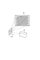
- FIG. 2 is a perspective view showing a schematic configuration of an image display apparatus using a laser light source and an optical deflector.
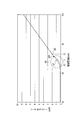
- FIG. 3 is a diagram illustrating an example of the IL characteristic of the semiconductor laser.
- FIG. 4 is a diagram showing a comparison between a normal semiconductor laser driving method and a semiconductor laser driving method in the image display apparatus according to the first embodiment.
- FIG. 5 is a diagram showing a comparison between a normal image display method and an image display method in the image display apparatus of the first embodiment.
- FIG. 6 is a diagram comparing pixel values expressed by one pixel in each of the normal image display method and the image display method in the image display apparatus of the first embodiment.
- FIG. 7 is a block diagram illustrating a light source driving device and an image display device according to the second embodiment.
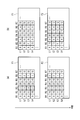
- FIG. 8 is a diagram illustrating a first example in which a normal image display method and an image display method in the image display apparatus according to the second embodiment are compared.
- FIG. 9 is a diagram illustrating a second example in which a normal image display method and an image display method in the image display apparatus according to the second embodiment are compared.
- FIG. 10 is a table summarizing, in a tabular form, how pixel values are replaced in the image display apparatus according to the second embodiment.
- FIG. 11 is a block diagram illustrating a light source driving device and an image display device according to the third embodiment.
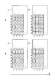
- FIG. 12 is a diagram illustrating an example in which a normal image display method and an image display method in the image display apparatus according to the third embodiment are compared.
- FIG. 13 shows an average value of pixel values of odd frames and even frames by a normal image display method, and an average value of pixel values of odd frames and even frames by an image display method in the image display device of the third embodiment. It is a figure for comparing.
- FIG. 14 is a table summarizing, in tabular form, how pixel values are replaced in the image display apparatus according to the third embodiment.
- the image display devices of the first and second embodiments are roughly configured by deflecting the laser light in a horizontal direction and a vertical direction, and a laser light generation unit 50 that emits laser light. And an optical deflector 100 for displaying an image on the screen 60.
- an optical deflector 100 includes a horizontal deflection element (not shown) for deflecting laser light in the horizontal direction and a vertical deflection element (not shown) for deflecting laser light in the vertical direction. It has a structured.
- the optical deflector 100 includes a mirror 12, a horizontal drive unit 11H, a vertical drive unit 11V, and a drive detection unit 13.
- the horizontal drive unit 11H is a drive mechanism that drives the mirror 12 in the horizontal direction
- the vertical drive unit 11V is a drive mechanism that drives the mirror 12 in the vertical direction.
- the drive detection unit 13 can be configured by a detection circuit using, for example, a Hall element or a piezoelectric element.
- the control unit 200 receives an image signal indicating an image to be displayed on the image display device.
- the image displayed on the image display device is an image with relatively little movement.
- the image signal is configured such that a plurality of the same frames are continued.
- the plurality of frames are preferably even numbers, but may be odd numbers.
- the control unit 200 includes a pixel value replacement unit 210 described later.
- the control unit 200 generates a horizontal drive signal for swinging the optical deflector 100 in the horizontal direction based on the horizontal synchronization signal of the input image signal, and supplies the horizontal drive signal to the horizontal drive unit 11H.
- the control unit 200 generates a vertical drive signal for swinging the optical deflector 100 in the vertical direction based on the vertical synchronization signal of the input image signal, and supplies the vertical drive signal to the vertical drive unit 11V.
- a drive detection signal generated by detecting the swing of the horizontal deflection element by the drive detection unit 13 is input to the control unit 200.
- the control unit 200 can be configured by, for example, a microprocessor or an FPGA (Field Programmable Gate Array).
- the driving unit 40 includes an R light source driving unit 40r, a G light source driving unit 40g, and a B light source driving unit 40b.
- the R light source drive unit 40r, the G light source drive unit 40g, and the B light source drive unit 40b drive the laser light generation unit 50 based on the control by the control unit 200.
- Each of the R light source driving unit 40r, the G light source driving unit 40g, and the B light source driving unit 40b can be configured by, for example, a constant current type driving circuit.
- the laser light generator 50 includes a light source 51, prisms 52 to 54, a mirror 55, and a lens 56.
- the light source 51 includes an R light source 51r that emits an R laser beam, a G light source 51g that emits a G laser beam, and a B light source 51b that emits a B laser beam.
- the R light source driving unit 40r drives the R light source 51r
- the G light source driving unit 40g drives the G light source 51g
- the B light source driving unit 40b drives the B light source 51b.
- the drive unit 40 supplies a drive signal whose pulse width is constant and whose drive current value increases or decreases according to the luminance value of the image to be displayed, specifically, the pixel value of each pixel constituting the image.
- Each of the light source 51r, the G light source 51g, and the B light source 51b is driven.
- the control unit 200 controls the drive unit 40 so as to supply the light source 51 with a drive signal having a drive current value corresponding to each pixel value.
- the prism 52 bends the optical path of the R laser beam emitted from the R light source 51r by 90 degrees.
- the prism 53 combines the R laser beam and the G laser beam.
- the prism 54 combines the combined light of the R laser light and the G laser light and the B laser light.
- the control unit 200 controls the driving unit 40 so that the combined light corresponding to the input image signal is output from the prism 54.
- the mirror 55 reflects the combined light of the R, G, and B laser beams output from the prism 54.
- the lens 56 collects the combined light from the mirror 55 and makes it incident on the mirror 12.
- 1 includes the light source driving device 260 according to the first embodiment.
- the mirror 12 is oscillated so that the laser beam is scanned in the horizontal direction of the screen 60 by the horizontal deflection element, and is oscillated so that the laser beam is scanned in the vertical direction of the screen 60 by the vertical deflection element.
- the image based on the image signal is displayed on the screen 60 by the horizontal and vertical scanning of the laser beam by the optical deflector 100.
- the optical deflector 100 and the light source driving device 260 in FIG. 1 constitute the image display device of the first embodiment.
- FIG. 3 shows the IL characteristics of the semiconductor laser that is one of the R light source 51r, the G light source 51g, and the B light source 51b.
- the semiconductor laser when the drive current value is equal to or greater than the threshold value Ith, the semiconductor laser emits laser light.
- the drive current value and the laser output power have a substantially linear relationship as a whole.
- point p1 is a point where the laser output power is 1 mW
- point p2 is a point where the laser output power is 2 mW.
- the point p1 is a point corresponding to the laser output power expressing the pixel value 2
- the point p2 is a point corresponding to the laser output power expressing the pixel value 4.
- the laser output power may be increased as the luminance value of the image signal indicated by the alternate long and short dash line increases.
- laser output power discrete 0.5, 1, 1.5, 2, 2.5,..., 7, 7.5, 8, 8.5 (mW) Only shows.
- the drive current values for obtaining the laser output power of 1, 2, 3, 4, 5, 6, 7, 8 (mW) are I1, I2, I3, I4, I5, I6, I7, and I8. According to FIG. 3, for example, the drive current value I1 is about 85 (mA), and the drive current value I2 is about 87 (mA).
- a kink region 30 exists in a region where the drive current value near the threshold value Ith is small, as surrounded by a one-dot chain line.
- the relationship between the drive current value and the laser output power is not linear. Since the IL characteristics of the R light source 51r, the G light source 51g, and the B light source 51b are not the same, the characteristics in the kink region 30 are different.
- the broken line shown in the kink region 30 in FIG. 3 shows a desirable linear characteristic between the drive current value and the laser output power. It is assumed that the laser output power within 1.5 mW is included in the kink region 30.
- the laser output power necessary for displaying a low-luminance image (pixel) is 1 mW, for example. If the inside of the kink region 30 has a linear characteristic as indicated by a broken line and the characteristics in the kink region 30 in the IL characteristics of the R light source 51r, the G light source 51g, and the B light source 51b are the same, the color shift is Almost does not occur.
- the characteristics in the kink region 30 are not linear, and the characteristics in the kink region 30 differ among the R light source 51r, the G light source 51g, and the B light source 51b. Therefore, color misregistration occurs.
- the control unit 200 when displaying each pixel constituting an image, the control unit 200 operates as follows.
- the pixel value replacement unit 210 converts the low-brightness pixel value to a larger laser output outside the kink region 30. Replace with pixel value expressed in power.
- the pixel value replacement unit 210 increases the laser output power by replacing the pixel value, so that the luminance value does not become larger than a predetermined low luminance to be displayed.
- the pixel value at the same position in the frame is replaced with 0.
- FIG. 5A shows a state before the pixel value is replaced by the pixel value replacement unit 210.
- FIG. 5A shows a state before the pixel value is replaced by the pixel value replacement unit 210.
- FIG. 5A shows a state before the pixel value is replaced by the pixel value replacement unit 210.
- FIG. 5A In the image signal, the same frame is assumed to be six consecutive frames F1 to F6, and here, four frames F1 to F4 are shown.
- the display method for displaying the frames F1 to F4 as shown in FIG. 5A as they are is a normal image display method.
- the frames F1 to F6 are formed by arranging pixels in the horizontal direction and the vertical direction.
- FIG. 5 shows only partial pixels Px1 to Px7. Here, for convenience of illustration, a state in which the number of pixels is significantly reduced is shown.
- the pixel value 2 of the pixel Px6 shown in FIG. 5A is a low-luminance pixel value represented by the laser output power in the kink region 30.
- the pixel value replacement unit 210 replaces the pixel value of the pixel Px6 of the frame F1 with the pixel value 4 expressed by the laser output power outside the kink region 30.
- the pixel value replacement unit 210 replaces the pixel value of the pixel Px6 of the frame F2 with the pixel value 0.
- the pixel value replacement unit 210 replaces the pixel value of the pixel Px6 in the frame F3 with the pixel value 4, and replaces the pixel value of the pixel Px6 in the frame F4 with the pixel value 0.
- FIG. 6 shows how the pixel value of the pixel Px6 is expressed by focusing on only the pixel Px6 in the frames F1 to F6.
- FIG. 6A shows a state in which the pixel value is not replaced by the pixel value replacement unit 210 as shown in FIG. That is, FIG. 6A corresponds to a normal image display method.
- the pixels Px6 of the frames F1 to F6 are displayed with a pixel value 2 expressed by the laser output power in the kink region 30. Actually, however, since the characteristics in the kink region 30 are not linear, the pixel values different from the pixel values 2 are displayed as indicated by the one-dot chain line.
- FIG. 6B shows a state where the pixel value is replaced by the pixel value replacement unit 210 as shown in FIG. 5B.
- the pixel Px6 of the frames F1, F3, and F5 is displayed with a pixel value 4 represented by the laser output power outside the kink region 30, and the pixel Px6 of the frames F2, F4, and F6 has a pixel value of 0. It is said.
- the pixel value of the pixel Px6 is displayed with an average pixel value of 2 as indicated by the alternate long and short dash line. Since the pixel value 4 is a pixel value expressed by the laser output power outside the kink region 30, almost no color misregistration occurs.
- the following may be done.
- the pixel values in half of the plurality of frames are doubled, and the pixel values in the remaining half frames Is set to 0.
- a pixel value at a predetermined pixel position in an image signal is a first pixel value expressed by a laser output power equal to or lower than a threshold that is a predetermined laser output power.
- the pixel value replacement unit 210 may replace the pixel values in the plurality of frames so that the average pixel value when the pixel values at the predetermined pixel positions are averaged in the plurality of frames becomes the first pixel value.
- the pixel value replacement unit 210 replaces a pixel value at a predetermined pixel position in any one of the plurality of frames with a second pixel value expressed by a laser output power exceeding a threshold value, and determines a predetermined value in another frame of the plurality of frames.
- the pixel value at the pixel position may be replaced with 0.
- the pixel value 2 expressed by the laser output power at the point p1 in the kink region 30 is taken as an example of the low luminance pixel. The same applies to the case where the pixel value is expressed by the laser output power other than the point p1 in the kink region 30.
- the pixel value replacement unit 210 may replace the pixel value of the pixel value 3 or less in the same manner as described above.
- the laser output power to be used is 2 mW or more as shown in FIG. It becomes.
- the point pth shown in FIG. 3 is a threshold value that is a predetermined laser output power indicating the inner and outer boundaries of the kink region 30.
- the control unit 200 may set the laser output power equal to or higher than the maximum laser output power in the kink region 30 in the IL characteristic of the semiconductor laser as the threshold value pth.
- the pixel value replacement unit 210 does not replace the pixel value.
- the pixel value replacement unit 210 is a part of a plurality of frames.
- the pixel value of this frame may be replaced with the second pixel value, the pixel values of other frames may be replaced with 0, and the average pixel value when averaged over a plurality of frames may be used as the first pixel value.
- the light source driving device 260 may be used other than the image display device.
- the control unit 200 may control the driving unit 40 as follows.
- the control unit 200 controls the drive unit 40 so that the drive current value of the drive signal supplied from the drive unit 40 to the light source 51 increases as the luminance value of the image signal for displaying an image increases.
- the image display device includes the optical deflector 100 that displays the image by deflecting the laser light emitted from the light source 51 in the horizontal direction and the vertical direction, and the light source driving device 260. Even when a low-luminance image is displayed, the occurrence of color misregistration can be suppressed.
- a control unit 201 is provided instead of the control unit 200.
- the control unit 201 receives a vertical synchronization signal and a horizontal synchronization signal which are not shown in FIG.
- the control unit 201 includes a pixel value replacement unit 211.
- the 7 includes the light source driving device 261 according to the second embodiment.
- the optical deflector 100 and the light source driving device 261 in FIG. 7 constitute the image display device of the second embodiment.
- the pixel value replacement unit 211 converts the low-brightness pixel value into the kink region. Replace with a pixel value represented by a larger laser output power outside of 30.
- the pixel value replacement unit 211 increases the laser output power by replacing the pixel value, so that the luminance value does not become larger than a predetermined low luminance to be displayed.
- the pixel value at the same position in the frame is replaced with 0.
- the pixel value replacement method is different between the odd-numbered frame and the even-numbered frame.
- FIG. 8A shows a state before pixel values are replaced by the pixel value replacement unit 211.
- FIG. 8A shows a state before pixel values are replaced by the pixel value replacement unit 211.
- FIG. 8A shows a state before pixel values are replaced by the pixel value replacement unit 211.
- FIG. 8A shows a state before pixel values are replaced by the pixel value replacement unit 211.
- FIG. 8A shows a state before pixel values are replaced by the pixel value replacement unit 211.
- FIG. 8A shows a state before pixel values are replaced by the pixel value replacement unit 211.
- FIG. 8A shows a state before pixel values are replaced by the pixel value replacement unit 211.
- FIG. 8A shows a state before pixel values are replaced by the pixel value replacement unit 211.
- FIG. 8A shows a state before pixel values are replaced by the pixel value replacement unit 211.
- FIG. 8A shows a state before pixel values are replaced by the pixel value replacement
- L1, L2, L3, L4 Indicate the row numbers of the frames F1, F2. L1, L3,... Are odd rows, and L2, L4,. R1, R2, R3, R4... Indicate pixel column numbers.
- the control unit 201 determines whether the frame of the image to be displayed is an odd frame or an even frame. Can be determined.
- control unit 201 can determine whether the pixel of the image to be displayed is an odd row pixel or an even row pixel.
- the pixel value of 3 or less is the first pixel value expressed by the laser output power equal to or lower than the threshold, which is the predetermined laser output power described above.
- the pixel value of an odd-numbered row having a pixel value of 3 or less is doubled, and the pixel value of an even-numbered row of pixels having a pixel value of 3 or less is set to 0.
- the pixel values of the odd-numbered pixels having the pixel value of 3 or less are set to 0, and the pixel values of the even-numbered pixels having the pixel value of 3 or less are doubled.
- the pixels in the rows L1 to L4 in the column R3 have pixel values 2, 3, 3, and 2, respectively, and are all the first pixel values.
- the pixels in the rows L1 to L4 in the column R6 have pixel values 2, 2, 1, and 1, respectively, and are all the first pixel values.
- the pixel value replacement unit 211 doubles the pixel value of the pixel in the row L1 in the columns R3 and R6 to obtain the pixel value 4 in the frame F1, and in the columns R3 and R6, respectively.
- the pixel value of the pixel in the row L3 is doubled to obtain pixel values 6 and 2, respectively.
- the pixel value replacement unit 211 sets the pixel values of the pixels in the rows L2 and L4 in the columns R3 and R6 to 0 in the frame F1.
- the pixel value replacement unit 211 sets the pixel values of the pixels in the rows L1 and L3 in the columns R3 and R6 to 0 in the frame F2.
- the pixel value replacement unit 211 doubles the pixel values of the pixels in the row L2 in the columns R3 and R6 to become pixel values 6 and 4, respectively, in the frame F2.
- the pixel values of the pixels in row L4 in columns R3 and R6 are doubled to become pixel values 4 and 2, respectively.
- the pixel value of some pixels remains the first pixel value after the pixel value replacement (pixel value 3 or less), but if the pixel value before replacement is 2 or more, All are replaced with the second pixel value expressed by the laser output power exceeding the threshold value.
- the operation of the pixel value replacement unit 211 will be specifically described with reference to a second example shown in FIG. As shown in FIG. 9A, in the second example, the pixel values of the pixels in the rows L2 and L3 in the column R3 are 5.
- the pixel value replacement unit 211 doubles the pixel value of the pixel in the row L1 in the column R3 in the frame F1, as shown in FIG. 9B.
- the pixel value is 4, and the pixel value of the pixel in the row L4 is 0.
- the pixel value replacement unit 211 sets the pixel value of the pixel in the row L1 in the column R3 to 0 and doubles the pixel value of the pixel in the row L4 in the frame F2.
- the pixel value is 4.
- FIG. 10 summarizes the pixel value replacement method in the pixel value replacement unit 211 in a tabular form.
- the pixel value replacement unit 211 doubles the pixels below the threshold in the odd rows (pixels having the first pixel value) and sets the pixels below the threshold in the even rows to 0.
- the pixel value replacement unit 211 sets the pixels below the threshold in the odd rows to 0, and doubles the pixels below the threshold in the even rows.
- the pixel value replacement unit 211 converts the pixel value regardless of the odd-numbered frame and the even-numbered row regardless of the odd-numbered frame and the even-numbered frame. Instead, the pixel value is used as it is.
- the pixel value replacement unit 211 may exchange the condition for doubling the pixel value and the condition for setting it to 0. That is, the pixel value replacement unit 211 sets the pixels below the threshold in the odd rows to 0 in the odd frame, doubles the pixels below the threshold in the even rows, and doubles the pixels below the threshold in the odd rows in the even frame.
- the pixels below the threshold value in even rows may be set to 0.
- the pixel value replacement unit 211 doubles the pixel value at the predetermined pixel position in the odd row and the pixel value at the predetermined pixel position in the even row in one of the odd frame and the even frame among the plurality of frames. It may be 0.
- the predetermined pixel position is the position of the pixel having the first pixel value expressed by the laser output power equal to or lower than the threshold as described above.
- the pixel value replacement unit 211 may set the pixel value at the predetermined pixel position in the odd row to 0 and the pixel value at the predetermined pixel position in the even row to 0 in the other frame of the odd frame and the even frame.
- the second embodiment described above in addition to the same effects as those of the first embodiment, the following effects can be obtained.
- the pixel values of adjacent rows in the same column do not become 0 at the same time. Therefore, compared to the first embodiment, it is possible to display a smooth image (moving image).
- control unit 202 is provided instead of the control unit 201.
- the control unit 202 includes a pixel value replacement unit 212.
- the drive unit 40, the laser light generation unit 50, and the control unit 202 in FIG. 11 constitute a light source drive device 262 of the third embodiment.
- the optical deflector 100 and the light source driving device 262 in FIG. 11 constitute the image display device of the third embodiment.
- FIG. 12A shows a state before the pixel value is replaced by the pixel value replacing unit 212.
- FIG. 12A shows a state before the pixel value is replaced by the pixel value replacing unit 212.
- FIG. 12A shows a state before the pixel value is replaced by the pixel value replacing unit 212.
- FIG. 12A shows a state before the pixel value is replaced by the pixel value replacing unit 212.
- FIG. 12A shows a state before the pixel value is replaced by the pixel value replacing unit 212.
- FIG. 12A shows a state before the pixel value is replaced by the pixel value replacing unit 212.
- FIG. 12A shows a state before the pixel value is replaced by the pixel value replacing unit 212.
- FIG. 12A shows a state before the pixel value is replaced by the pixel value replacing unit 212.
- FIG. 12A shows a state before the pixel value is replaced by the pixel value replacing unit 212.
- FIG. 12A shows a state before the
- the pixel value of 3 or less is the first pixel value expressed by the laser output power equal to or lower than the threshold, which is the predetermined laser output power described above.
- the threshold which is the predetermined laser output power described above.
- the pixel values of the pixels in the rows L1 and L4 in the column R3 and the rows L1 to L4 in the column R6 are equal to or less than the pixel value 3
- the frame F2 in the column F2 the column F2
- the pixel values of the pixels in the row L1 in R3 and the rows L3 and L4 in the column R6 are equal to or less than the pixel value 3.
- the pixel value of the odd-numbered row is changed to the pixel value of the odd-numbered frame and the even-numbered frame.
- the pixel value of pixels in even rows are set to 0.
- the pixel value of the odd-numbered row is set to 0 and the pixel value of the even-numbered row is set to the odd-numbered frame.
- the sum of the pixel value and the pixel value of the even frame is used.
- the pixels in the rows L1 and L4 in the column R3 and the pixels in the rows L1 to L4 in the column R6 have a pixel value of 3 or less, and the pixel whose pixel value is to be replaced It becomes.
- each pixel in the row L1 in the column R3 and the rows L3 and L4 in the column R6 has a pixel value of 3 or less, and is a pixel to be replaced.
- each pixel in the row L4 in the column R3 and each of the rows L1 and L2 in the column R6 exceeds the pixel value 3, but the pixel at the same position in the frame F1 is less than or equal to the pixel value 3, so the pixel value is replaced. This is the target pixel.
- the pixel value replacement unit 212 As shown in FIG. 12B, the pixel values 2, 2, and 2 of the pixels in the odd rows L1 and the odd rows L1 and L3 in the column R3. 1 and the pixel values 3, 5, and 3 of the pixels at the same position in the frame F2 are added, and the pixel values 2, 2, and 1 are replaced with pixel values 5, 7, and 4, which are addition values.
- the pixel value replacement unit 212 As shown in FIG. 12B, the pixel values 2 of the pixels in the even-numbered rows L4 and the even-numbered rows L2, L4 in the column R3. 2 and 3 are all replaced with a pixel value of 0.
- the pixel value replacement unit 212 sets all the pixel values 2, 5, and 3 of the pixels in the row L1 in the column R3 and the rows L1 and L3 in the column R6. Replace with the value 0.
- the pixel values 2, 2, and 3 of the pixels at the same position in are added, and the pixel values 5, 5, and 2 are replaced with the pixel values 7, 7, and 5, which are addition values.
- FIG. 13A shows the average value Ave (F1, FF2) of the frames F1 and F2 shown in FIG.
- FIG. 13B shows the average value Ave (F1, F2) of the frames F1 and F2 shown in FIG.
- the average value Ave (F1, F2) is the same before and after the pixel value replacement by the pixel value replacement unit 212.
- FIG. 14 summarizes the pixel value replacement method in the pixel value replacement unit 212 in a tabular form.
- the pixel value replacement unit 212 executes the following replacement process when any pixel has a threshold value or less (the pixel having the first pixel value) at the same pixel position in the odd frame and the even frame.
- the pixel values at the same pixel positions in the odd and even frames are added in the odd row, and the original pixel value is replaced with the added value.
- the original pixel value is replaced with the pixel value 0. To do.
- the original pixel value is replaced with the pixel value 0 in the odd row, and the pixel value at the same pixel position in the odd frame and the even frame is added in the even row, and the original pixel value is replaced with the added value. To do.
- the pixel value replacement unit 212 sets the odd row and the odd row regardless of the odd frame and the even frame. Regardless of the even-numbered row, the pixel value is not converted and is used as it is.
- the pixel value replacement unit 212 may exchange the condition for setting the pixel value to the added value and the condition for setting the value to 0. That is, the pixel value replacement unit 212 replaces the pixel value with 0 in the odd-numbered row in the odd-numbered frame, replaces with the added value in the even-numbered row, replaces with the added value in the odd-numbered row in the even-numbered frame, You may substitute 0.
- the following effects are obtained in addition to the same effects as those of the first and second embodiments.
- an image can be displayed without using a low-brightness pixel value represented by the laser output power in the kink region 30. .
- the same pixel value is not always continuous in successive frames.
- the same frame often continues in succession, but the same frame does not continue when the image is changed at high speed. Sometimes.
- the third embodiment can be used even when the same frame is not continuous.
- the optical deflector 100 is preferably configured using MEMS technology, but is not limited thereto.
- the optical deflector 100 only needs to have a function of deflecting laser light in the horizontal direction and the vertical direction, and the specific configuration is not particularly limited.
- the present invention can be used for a light source driving device that drives a semiconductor laser and an image display device that displays an image by scanning laser light with an optical deflector.
Landscapes
- Physics & Mathematics (AREA)
- General Physics & Mathematics (AREA)
- Engineering & Computer Science (AREA)
- Optics & Photonics (AREA)
- Computer Hardware Design (AREA)
- Theoretical Computer Science (AREA)
- Condensed Matter Physics & Semiconductors (AREA)
- Electromagnetism (AREA)
- Control Of Indicators Other Than Cathode Ray Tubes (AREA)
- Mechanical Optical Scanning Systems (AREA)
Abstract
半導体レーザよりなる光源(51)は、レーザ光を射出する。駆動部(40)は、光源(51)を駆動する。画素値置換部(210)は、所定画素位置における画素値が、閾値以下のレーザ出力パワーで表現される第1の画素値を含むとき、所定画素位置における画素値を複数フレームで平均したときの平均画素値が第1の画素値となるよう、複数フレームのいずれかのフレームにおける所定画素位置における画素値を、閾値を超えるレーザ出力パワーで表現される第2の画素値に置換し、複数フレームの他のフレームにおける所定画素位置における画素値を0に置換する。制御部(200)は、画素値置換部(210)によって画素値が置換された状態の画像信号に基づいて光源(51)を駆動するよう、駆動部(40)を制御する。
Description
本開示は、半導体レーザを駆動する光源駆動装置、及び、光偏向器を用いた画像表示装置に関する。
近年、MEMS(Micro Electro Mechanical System)技術を用いた光偏向器が開発されている。光偏向器は、画像を表示させるための表示デバイスとして用いられる。光偏向器のミラーに半導体レーザより射出されたレーザ光を照射し、ミラーを2次元的に偏向させる。これによって、光偏向器は、レーザ光を水平方向及び垂直方向に走査させて、スクリーンに画像を表示させることができる。
特許文献1に記載されているように、光偏向器は例えば車両用のヘッドアップディスプレイに使用されることがある。ヘッドアップディスプレイは、画像表示装置の一例である。
半導体レーザを駆動する駆動電流値と半導体レーザより射出されるレーザ光のレーザ出力パワーとに間には、I-L特性と称される関係がある。駆動電流値が所定の閾値以上になると、半導体レーザはレーザ光を射出する。I-L特性によれば、駆動電流値を増大させるとレーザ出力パワーはほぼリニアに増大する。
例えば夜間においては、画像表示装置によって表示する画像の輝度を低くすることが求められることがある。低輝度の画像を表示するには、駆動電流値を小さくしてレーザ出力パワーを小さくすればよい。
ところが、閾値付近の駆動電流値が小さい領域には、レーザ出力パワーがリニアに増大しないキンク領域が存在する。従って、レーザ出力パワーを小さくするために、駆動電流値を小さくすると、キンク領域内の駆動電流値に基づくレーザ出力パワーでレーザ光が発せられることになる。
赤色(R)光、緑色(G)光、青(B)光を射出するそれぞれの半導体レーザが有するI-L特性は互いに異なる。従って、キンク領域内の駆動電流値に基づくレーザ出力パワーで、R,G,B光それぞれのレーザ光を発生させると、本来得ようとした色とは異なる色ずれが発生してしまう。
実施形態は、低輝度の画像を表示する場合でも色ずれの発生を抑えることができる光源駆動装置及び画像表示装置を提供することを目的とする。
実施形態の第1の態様によれば、レーザ光を射出する半導体レーザよりなる光源と、前記光源を、画像信号におけるそれぞれの画素値に応じて駆動電流値を増減させる駆動信号によって駆動する駆動部と、前記画像信号における連続する複数フレームの所定画素位置における画素値が、所定のレーザ出力パワーである閾値以下のレーザ出力パワーで表現される第1の画素値を含むとき、前記所定画素位置における画素値を前記複数フレームで平均したときの平均画素値が前記第1の画素値となるよう、前記複数フレームのいずれかのフレームにおける前記所定画素位置における画素値を、前記閾値を超えるレーザ出力パワーで表現される第2の画素値に置換し、前記複数フレームの他のフレームにおける前記所定画素位置における画素値を0に置換する画素値置換部と、前記画素値置換部によって前記所定画素位置における画素値が置換された状態の画像信号に基づいて前記光源を駆動するよう、前記駆動部を制御する制御部とを備えることを特徴とする光源駆動装置が提供される。
実施形態の第2の態様によれば、上記の光源駆動装置と、前記光源より発せられたレーザ光を水平方向及び垂直方向に偏向して画像を表示させる光偏向器とを備えることを特徴とする画像表示装置が提供される。
実施形態の光源駆動装置及び画像表示装置によれば、低輝度の画像を表示する場合でも色ずれの発生を抑えることができる。
以下、第1,第2実施形態の光源駆動装置及び画像表示装置について、添付図面を参照して説明する。図2に示すように、第1,第2実施形態の画像表示装置は、概略的には、レーザ光を射出するレーザ光発生部50と、レーザ光を水平方向及び垂直方向に偏向させて、スクリーン60に画像を表示させる光偏向器100とを備える。
<第1実施形態>
図1を用いて、第1実施形態の光源駆動装置及び画像表示装置の詳細な構成及び動作を説明する。図1において、光偏向器100は、レーザ光を水平方向に偏向するための水平偏向素子(図示せず)とレーザ光を垂直方向に偏向するための垂直偏向素子(図示せず)とが一体化された構成を有する。
図1を用いて、第1実施形態の光源駆動装置及び画像表示装置の詳細な構成及び動作を説明する。図1において、光偏向器100は、レーザ光を水平方向に偏向するための水平偏向素子(図示せず)とレーザ光を垂直方向に偏向するための垂直偏向素子(図示せず)とが一体化された構成を有する。
光偏向器100は、ミラー12,水平駆動部11H,垂直駆動部11V,駆動検出部13を有する。水平駆動部11Hはミラー12を水平方向に駆動する駆動機構であり、垂直駆動部11Vはミラー12を垂直方向に駆動する駆動機構である。駆動検出部13は、例えばホール素子や圧電素子を使用した検出回路によって構成することができる。
制御部200には、画像表示装置で表示する画像を示す画像信号が入力される。画像表示装置で表示する画像は比較的動きが少ない画像である。画像信号は、同じフレームが複数フレーム連続するように構成されている。複数フレームは偶数であることが好ましいが、奇数であっても構わない。制御部200は、後述する画素値置換部210を有する。
制御部200は、入力された画像信号の水平同期信号に基づいて、光偏向器100を水平方向に揺動させるための水平駆動信号を生成して水平駆動部11Hに供給する。
制御部200は、入力された画像信号の垂直同期信号に基づいて、光偏向器100を垂直方向に揺動させるための垂直駆動信号を生成して垂直駆動部11Vに供給する。駆動検出部13によって水平偏向素子の揺動を検出することによって生成された駆動検出信号は、制御部200に入力される。制御部200は、例えばマイクロプロセッサまたはFPGA(Field Programmable Gate Array)等で構成することができる。
駆動部40は、R光源駆動部40r,G光源駆動部40g,B光源駆動部40bを有する。R光源駆動部40r,G光源駆動部40g,B光源駆動部40bは、制御部200による制御に基づいて、レーザ光発生部50を駆動する。R光源駆動部40r,G光源駆動部40g,B光源駆動部40bは、それぞれ、例えば定電流方式の駆動回路によって構成することができる。
レーザ光発生部50は、光源51と、プリズム52~54と、ミラー55と、レンズ56とを有する。光源51は、それぞれ半導体レーザよりなる、Rのレーザ光を射出するR光源51rと、Gのレーザ光を射出するG光源51gと、Bのレーザ光を射出するB光源51bとよりなる。
R光源駆動部40rはR光源51rを駆動し、G光源駆動部40gはG光源51gを駆動し、B光源駆動部40bはB光源51bを駆動する。駆動部40は、パルス幅が一定で、表示する画像の輝度値、具体的には、画像を構成するそれぞれの画素の画素値に応じて駆動電流値が増減する駆動信号を供給して、R光源51r,G光源51g,B光源51bそれぞれを駆動する。
制御部200は、光源51にそれぞれの画素値に応じた駆動電流値を有する駆動信号を供給するよう、駆動部40を制御する。
プリズム52は、R光源51rより発せられたRのレーザ光の光路を90度折り曲げる。プリズム53はRのレーザ光とGのレーザ光とを合成する。プリズム54は、Rのレーザ光とGのレーザ光との合成光とBのレーザ光とを合成する。
制御部200は、入力された画像信号に応じた合成光がプリズム54より出力されるよう、駆動部40を制御する。ミラー55は、プリズム54より出力されたR,G,Bのレーザ光の合成光を反射する。レンズ56は、ミラー55からの合成光を集光してミラー12へと入射させる。
図1における駆動部40とレーザ光発生部50と制御部200とは、第1実施形態の光源駆動装置260を構成する。
ミラー12は、水平偏向素子によってレーザ光をスクリーン60の水平方向に走査させるよう揺動され、垂直偏向素子によってレーザ光をスクリーン60の垂直方向に走査させるよう揺動される。
光偏向器100によるレーザ光の水平方向及び垂直方向の走査によって、スクリーン60には画像信号に基づく画像が表示される。
図1における光偏向器100と光源駆動装置260とは、第1実施形態の画像表示装置を構成する。
図3は、R光源51r,G光源51g,B光源51bのうちのいずれかである半導体レーザが有するI-L特性を示している。図3に示すように、駆動電流値が閾値Ith以上になると、半導体レーザはレーザ光を射出する。駆動電流値とレーザ出力パワーとは全体的にはほぼリニアな関係を有する。
図3において、ポイントp1はレーザ出力パワーが1mWのポイントであり、ポイントp2はレーザ出力パワーが2mWのポイントである。ポイントp1は、画素値2を表現するレーザ出力パワーに対応したポイントであり、ポイントp2は、画素値4を表現するレーザ出力パワーに対応したポイントであるとする。
まず、仮にI-L特性が全体としてリニアな特性であるとする。図4の(a)に示すように、一点鎖線にて示す画像信号の輝度値が大きくなるに従って、レーザ出力パワーを増大させればよい。ここでは、説明を容易にするため、レーザ出力パワーとして、離散的な0.5,1,1.5,2,2.5,…,7,7.5,8,8.5(mW)のみを示している。
1,2,3,4,5,6,7,8(mW)のレーザ出力パワーを得るための駆動電流値をI1,I2,I3,I4,I5,I6,I7,I8とする。図3によれば、例えば、駆動電流値I1は85(mA)程度、駆動電流値I2は87(mA)程度である。
図3に示すように、閾値Ith付近の駆動電流値が小さい領域には、一点鎖線で囲んでいるように、キンク領域30が存在する。キンク領域30では、駆動電流値とレーザ出力パワーとの関係はリニアではない。R光源51r,G光源51g,B光源51bそれぞれが有するI-L特性は同じではないため、キンク領域30における特性は異なる。
図3のキンク領域30内に示す破線は、駆動電流値とレーザ出力パワーとの望ましいリニアな特性を示している。なお、レーザ出力パワー1.5mW以内は、キンク領域30内に含まれているとする。
図3において、低輝度の画像(画素)を表示するために必要なレーザ出力パワーが例えば1mWであったとする。キンク領域30内が破線で示すようにリニアな特性であり、R光源51r,G光源51g,B光源51bそれぞれが有するI-L特性におけるキンク領域30内の特性が同じであれば、色ずれはほぼ発生しない。
ところが実際には、キンク領域30内の特性はリニアではなく、キンク領域30内の特性はR光源51r,G光源51g,B光源51bそれぞれで異なる。よって、色ずれが発生してしまう。
そこで、第1実施形態においては、画像を構成するそれぞれの画素を表示するとき、制御部200は次のように動作する。画素が、キンク領域30内のレーザ出力パワーで表現される所定の低輝度の画素値を有する場合には、画素値置換部210は、低輝度の画素値をキンク領域30外のより大きいレーザ出力パワーで表現される画素値に置換する。
このとき、画素値置換部210は、画素値を置換したことによってレーザ出力パワーが増大し、表示させようとする所定の低輝度よりも輝度値が大きくならないよう、複数の同じフレームのうちの残りのフレームにおける同一位置の画素値を0に置換する。
図5を用いて、画素値置換部210の動作をさらに説明する。図5において、(a)は、画素値置換部210によって画素値を置換する前の状態を示している。画像信号は同じフレームがフレームF1~F6の6フレーム連続するとし、ここでは、フレームF1~F4の4フレームを示している。図5の(a)に示すフレームF1~F4をそのまま表示する表示方法は、通常の画像表示方法である。
フレームF1~F6は、画素が水平方向及び垂直方向に配列されて形成される。図5においては、部分的な画素Px1~Px7のみを図示している。ここでは図示の都合上、画素数を大幅に少なくした状態を示している。
図5の(a)に示す画素Px6が有する画素値2は、キンク領域30内のレーザ出力パワーで表現される低輝度の画素値である。図5の(b)に示すように、画素値置換部210は、フレームF1の画素Px6の画素値を、キンク領域30外のレーザ出力パワーで表現される画素値4に置換する。画素値置換部210は、フレームF2の画素Px6の画素値を画素値0に置換する。
同様に、画素値置換部210は、フレームF3の画素Px6の画素値を画素値4に置換し、フレームF4の画素Px6の画素値を画素値0に置換する。図5では図示していないフレームF5,F6においても同様である。
図6は、フレームF1~F6における画素Px6のみに着目して、画素Px6の画素値がどのように表現されるかを示している。図6の(a)は、図5の(a)のように、画素値置換部210によって画素値を置換しない状態を示している。即ち、図6の(a)は、通常の画像表示方法に相当する。
図6の(a)では、フレームF1~F6の画素Px6がキンク領域30内のレーザ出力パワーで表現される画素値2で表示される。ところが実際には、キンク領域30内の特性はリニアではないため、一点鎖線で示すように、画素値2とは異なる画素値で表示されることになる。
一点鎖線の位置は、R光源51r,G光源51g,B光源51bそれぞれの特性のばらつきにより異なるため、色ずれが発生する。
図6の(b)は、図5の(b)のように、画素値置換部210によって画素値を置換した状態を示している。図6の(b)では、フレームF1,F3,F5の画素Px6がキンク領域30外のレーザ出力パワーで表現される画素値4で表示され、フレームF2,F4,F6の画素Px6が画素値0とされる。
よって、図6の(b)のフレームF1~F6全体で見たときには、画素Px6の画素値は、一点鎖線で示すように、平均の画素値2で表示されることになる。画素値4はキンク領域30外のレーザ出力パワーで表現される画素値であるため、色ずれはほとんど発生しない。
同じフレームが複数フレーム連続するときの複数フレームが偶数であれば、次のようにすればよい。キンク領域30内のレーザ出力パワーで表現される低輝度の画素を表示する際に、複数フレームのうちの1/2のフレームにおける画素値を2倍し、残りの1/2のフレームにおける画素値を0とする。
複数フレームが奇数であれば、複数フレームの全体の平均が表示しようとする画素値となるように、複数フレームのうちの部分的なフレームにおける画素値を増大して、残りのフレームにおける画素値を0とすればよい。
画像信号における所定画素位置における画素値が、所定のレーザ出力パワーである閾値以下のレーザ出力パワーで表現される第1の画素値であるとする。画素値置換部210は、所定画素位置における画素値を複数フレームで平均したときの平均画素値が第1の画素値となるように複数フレームにおける画素値を置換すればよい。
画素値置換部210は、複数フレームのいずれかのフレームにおける所定画素位置における画素値を、閾値を超えるレーザ出力パワーで表現される第2の画素値に置換し、複数フレームの他のフレームにおける所定画素位置における画素値を0に置換すればよい。
以上の説明においては、低輝度の画素として、キンク領域30内のポイントp1のレーザ出力パワーによって表現される画素値2を例としている。キンク領域30内のポイントp1以外のレーザ出力パワーによって画素値を表現する場合も同様である。
例えば、画素値3がレーザ出力パワー1.5mWで表現される画素値であるとすれば、画素値置換部210は、画素値3以下の画素値を上記と同様にして置換すればよい。第1実施形態によれば、レーザ出力パワー1.5mW以下は使用されないことになるので、使用されるレーザ出力パワーは、離散的に説明すれば、図4の(b)に示すように2mW以上となる。
図3に示すポイントpthは、キンク領域30の内外の境界を示す、所定のレーザ出力パワーである閾値とする。制御部200(画素値置換部210)は、半導体レーザが有するI-L特性におけるキンク領域30内の最大のレーザ出力パワー以上のレーザ出力パワーを閾値pthとして設定すればよい。
制御部200が、光源51が出力するレーザ光によって、閾値pthを超える第1のレーザ出力パワーに対応した輝度の画素値を表現させる場合には、画素値置換部210は、画素値を置換しない。
制御部200が、光源51が出力するレーザ光によって、閾値pth以下の第2のレーザ出力パワーに対応した輝度の画素値を表現させる場合には、画素値置換部210は、複数フレームにおける一部のフレームの画素値を第2の画素値に置換し、他のフレームの画素値を0に置換して、複数フレームで平均したときの平均画素値を第1の画素値とすればよい。
光源駆動装置260は、画像表示装置以外に用いられてもよい。光源駆動装置260が、光源51が射出するレーザ光によって画像を表示させる画像表示装置に用いられる場合には、制御部200は、駆動部40を次のように制御すればよい。
制御部200は、画像を表示させるための画像信号の輝度値が大きくなるほど駆動部40が光源51に供給する駆動信号の駆動電流値を増大させるよう、駆動部40を制御する。
以上のようにして、光源51より発せられたレーザ光を水平方向及び垂直方向に偏向して画像を表示させる光偏向器100と、光源駆動装置260とを備える第1実施形態の画像表示装置は、低輝度の画像を表示する場合でも色ずれの発生を抑えることができる。
<第2実施形態>
図7を用いて、第2実施形態の光源駆動装置及び画像表示装置の構成及び動作を説明する。図7において、図1に示す第1実施形態の光源駆動装置及び画像表示装置と同一部分には同一符号を付し、その説明を省略することがある。
図7を用いて、第2実施形態の光源駆動装置及び画像表示装置の構成及び動作を説明する。図7において、図1に示す第1実施形態の光源駆動装置及び画像表示装置と同一部分には同一符号を付し、その説明を省略することがある。
第2実施形態の光源駆動装置及び画像表示装置においては、制御部200の代わりに制御部201を設けている。制御部201には、図1では図示が省略されている垂直同期信号及び水平同期信号が入力される。制御部201は、画素値置換部211を有する。
図7における駆動部40とレーザ光発生部50と制御部201とは、第2実施形態の光源駆動装置261を構成する。図7における光偏向器100と光源駆動装置261とは、第2実施形態の画像表示装置を構成する。
第2実施形態においても、画素が、キンク領域30内のレーザ出力パワーで表現される所定の低輝度の画素値を有する場合には、画素値置換部211は、低輝度の画素値をキンク領域30外のより大きいレーザ出力パワーで表現される画素値に置換する。
このとき、画素値置換部211は、画素値を置換したことによってレーザ出力パワーが増大し、表示させようとする所定の低輝度よりも輝度値が大きくならないよう、複数の同じフレームのうちの残りのフレームにおける同一位置の画素値を0に置換する。
但し、第2実施形態においては、奇数フレームと偶数フレームとで、画素値の置換の仕方を異ならせる。
図8に示す第1の例を用いて、画素値置換部211の動作を具体的に説明する。図8において、(a)は、画素値置換部211によって画素値を置換する前の状態を示している。画像信号は同じフレームがフレームF1,F2の2フレーム連続している。フレームF1は奇数フレーム、フレームF2は偶数フレームである。
L1,L2,L3,L4…はフレームF1,F2の行番号を示している。L1,L3…は奇数行であり、L2,L4…は偶数行である。R1,R2,R3,R4…は画素の列番号を示している。
制御部201には、垂直同期信号及び水平同期信号が入力されるため、制御部201(画素値置換部211)は、表示しようとしている画像のフレームが奇数フレームであるのか偶数フレームであるのかを判別することができる。
また、制御部201(画素値置換部211)は、表示しようとしている画像の画素が奇数行の画素であるのか偶数行の画素であるのかを判別することができる。
ここで、画素値3以下が、上述した所定のレーザ出力パワーである閾値以下のレーザ出力パワーで表現される第1の画素値であるとする。
第2実施形態においては、奇数フレームでは、画素値3以下の奇数行の画素の画素値を2倍し、画素値3以下の偶数行の画素の画素値を0とする。一方、偶数フレームでは、画素値3以下の奇数行の画素の画素値を0とし、画素値3以下の偶数行の画素の画素値を2倍する。
具体的には次のとおりである。図8の(a)に示すように、列R3における行L1~L4の画素は画素値がそれぞれ2,3,3,2であり、いずれも第1の画素値である。列R6における行L1~L4の画素は画素値がそれぞれ2,2,1,1であり、いずれも第1の画素値である。
画素値置換部211は、図8の(b)に示すように、フレームF1では、列R3,R6における行L1の画素の画素値を2倍してそれぞれ画素値4とし、列R3,R6における行L3の画素の画素値を2倍してそれぞれ画素値6,2とする。
これと同時に、画素値置換部211は、図8の(b)に示すように、フレームF1では、列R3,R6における行L2,L4の画素の画素値を0とする。
一方、画素値置換部211は、図8の(b)に示すように、フレームF2では、列R3,R6における行L1,L3の画素の画素値を0とする。
これと同時に、画素値置換部211は、図8の(b)に示すように、フレームF2では、列R3,R6における行L2の画素の画素値を2倍してそれぞれ画素値6,4とし、列R3,R6における行L4の画素の画素値を2倍してそれぞれ画素値4,2とする。
図8に示す第1の例では、一部の画素で画素値置換後も依然として第1の画素値のまま(画素値3以下)となるが、置換前の画素値が2以上であれば、全て閾値を超えるレーザ出力パワーで表現される第2の画素値へと置換されることになる。
さらに、図9に示す第2の例を用いて、画素値置換部211の動作を具体的に説明する。図9の(a)に示すように、第2の例においては、列R3における行L2,L3の画素の画素値が5である。
この場合も、上述した画素値の置換の仕方に従って、画素値置換部211は、図9の(b)に示すように、フレームF1では、列R3における行L1の画素の画素値を2倍して画素値4とし、行L4の画素の画素値を0とする。
一方、画素値置換部211は、図9の(b)に示すように、フレームF2では、列R3における行L1の画素の画素値を0とし、行L4の画素の画素値を2倍して画素値4とする。
図10は、画素値置換部211における画素値の置換の仕方を表形式にまとめたものである。画素値置換部211は、奇数フレームでは、奇数行における閾値以下の画素(第1の画素値を有する画素)を2倍し、偶数行における閾値以下の画素を0とする。
画素値置換部211は、偶数フレームでは、奇数行における閾値以下の画素を0とし、偶数行における閾値以下の画素を2倍する。
画素が閾値を超えれば(第2の画素値を有する画素であれば)、画素値置換部211は、奇数フレームと偶数フレームに関係なく、奇数行と偶数行に関係なく、画素値を変換せず、そのままの画素値とする。
勿論、画素値置換部211は、画素値を2倍にする条件と0にする条件とを入れ替えてもよい。即ち、画素値置換部211は、奇数フレームでは、奇数行における閾値以下の画素を0とし、偶数行における閾値以下の画素を2倍し、偶数フレームでは、奇数行における閾値以下の画素を2倍し、偶数行における閾値以下の画素を0としてもよい。
画素値置換部211は、複数フレームのうち、奇数フレームと偶数フレームとのうちの一方のフレームでは、奇数行における所定画素位置における画素値を2倍し、偶数行における所定画素位置における画素値を0とすればよい。
所定画素位置とは、上記のように、閾値以下のレーザ出力パワーで表現される第1の画素値となっている画素の位置である。
画素値置換部211は、奇数フレームと偶数フレームとのうちの他方のフレームでは、奇数行における所定画素位置における画素値を0とし、偶数行における所定画素位置における画素値を0とすればよい。
以上説明した第2実施形態によれば、第1実施形態と同様の効果に加えて、次の効果を奏する。第2実施形態によれば、同じ列で隣接する行の画素値が同時に0となることはないため、第1実施形態と比較すると、滑らかな画像(動画)を表示することが可能となる。
<第3実施形態>
図11を用いて、第3実施形態の光源駆動装置及び画像表示装置の構成及び動作を説明する。図11において、図7に示す第2実施形態の光源駆動装置及び画像表示装置と同一部分には同一符号を付し、その説明を省略することがある。
図11を用いて、第3実施形態の光源駆動装置及び画像表示装置の構成及び動作を説明する。図11において、図7に示す第2実施形態の光源駆動装置及び画像表示装置と同一部分には同一符号を付し、その説明を省略することがある。
第3実施形態の光源駆動装置及び画像表示装置においては、制御部201の代わりに制御部202を設けている。制御部202は、画素値置換部212を有する。
図11における駆動部40とレーザ光発生部50と制御部202とは、第3実施形態の光源駆動装置262を構成する。図11における光偏向器100と光源駆動装置262とは、第3実施形態の画像表示装置を構成する。
図12に示す一例を用いて、画素値置換部212の動作を具体的に説明する。図12において、(a)は、画素値置換部212によって画素値を置換する前の状態を示している。フレームF1は奇数フレーム、フレームF2は偶数フレームであり、フレームF1とフレームF2とは同じではない。L1,L2,L3,L4…とR1,R2,R3,R4…の定義は、図8,図9と同じである。
ここで、画素値3以下が、上述した所定のレーザ出力パワーである閾値以下のレーザ出力パワーで表現される第1の画素値であるとする。図12の(a)に示す例では、フレームF1においては、列R3における行L1,L4と列R6における行L1~L4の画素の画素値が画素値3以下であり、フレームF2においては、列R3における行L1と列R6における行L3,L4の画素の画素値が画素値3以下である。
第3実施形態においては、奇数フレームでは、奇数フレームと偶数フレームの同一位置での画素値のいずれかが画素値3以下の場合、奇数行の画素の画素値を奇数フレームの画素値と偶数フレームの画素値との加算値とし、偶数行の画素の画素値を0とする。
一方、偶数フレームでは、奇数フレームと偶数フレームの同一位置での画素値のいずれか画素値3以下が場合、奇数行の画素の画素値を0とし、偶数行の画素の画素値を奇数フレームの画素値と偶数フレームの画素値との加算値とする。
具体的には次のとおりである。図12の(a)に示すように、フレームF1では、列R3における行L1,L4と列R6における行L1~L4のそれぞれの画素が画素値3以下であり、画素値を置換する対象の画素となる。
フレームF2では、列R3における行L1と列R6における行L3,L4のそれぞれの画素が画素値3以下であり、画素値を置換する対象の画素となる。これに加えて、列R3における行L4と列R6における行L1,L2のそれぞれの画素は画素値3を超えるが、フレームF1における同じ位置の画素が画素値3以下であるため、画素値を置換する対象の画素となる。
フレームF1では、画素値置換部212は、図12の(b)に示すように、列R3における奇数行の行L1と列R6における奇数行の行L1,L3の画素の画素値2,2,1とフレームF2における同じ位置の画素の画素値3,5,3とを加算して、画素値2,2,1を加算値である画素値5,7,4に置換する。
また、フレームF1では、画素値置換部212は、図12の(b)に示すように、列R3における偶数行の行L4と列R6における偶数行の行L2,L4の画素の画素値2,2,3を全て画素値0に置換する。
一方、フレームF2では、画素値置換部212は、図12の(b)に示すように、列R3における行L1と列R6の行L1,L3の画素の画素値2,5,3を全て画素値0に置換する。
また、フレームF2では、画素値置換部212は、図12の(b)に示すように、列R3における行L4と列R6における行L2,L4の画素の画素値5,5,2とフレームF1における同じ位置の画素の画素値2,2,3とを加算して、画素値5,5,2を加算値である画素値7,7,5に置換する。
図13の(a)は、図12の(a)に示すフレームF1,F2の平均値Ave(F1, F2)を示している。図13の(b)は、図12の(b)に示すフレームF1,F2の平均値Ave(F1, F2)を示している。画素値置換部212によって画素値を置換する前と置換した後とで平均値Ave(F1, F2)は同じとなる。
図14は、画素値置換部212における画素値の置換の仕方を表形式にまとめたものである。画素値置換部212は、奇数フレーム及び偶数フレームの同じ画素位置でいずれかの画素が閾値以下を有する(第1の画素値を有する画素である)とき、次のような置換処理を実行する。
奇数フレームでは、奇数行において、奇数フレーム及び偶数フレームの同じ画素位置の画素値を加算して、元の画素値を加算値に置換し、偶数行において、元の画素値を画素値0に置換する。
偶数フレームでは、奇数行において、元の画素値を画素値0に置換し、偶数行において、奇数フレーム及び偶数フレームの同じ画素位置の画素値を加算して、元の画素値を加算値に置換する。
画素値置換部212は、奇数フレーム及び偶数フレームの同じ画素位置で双方の画素が閾値を超える(第2の画素値を有する画素である)とき、奇数フレームと偶数フレームに関係なく、奇数行と偶数行に関係なく、画素値を変換せず、そのままの画素値とする。
勿論、画素値置換部212は、画素値を加算値にする条件と0にする条件とを入れ替えてもよい。即ち、画素値置換部212は、奇数フレームでは、奇数行において画素値0に置換し、偶数行において加算値に置換し、偶数フレームでは、奇数行において加算値に置換し、偶数行において画素値0に置換してもよい。
以上説明した第3実施形態によれば、第1及び第2の実施形態と同様の効果に加えて、次の効果を奏する。第3実施形態によれば、連続するフレームで同じ画素値が存在しなくても、キンク領域30内のレーザ出力パワーで表現される低輝度の画素値を使用しないで画像を表示することができる。
自然画や映画等の動画像を表示する場合、連続するフレームで同じ画素値が連続するとは限らない。また、ナビゲーション画像や燃料残量等の車両に関連する情報を表示するとき、一般的には同じフレームが複数連続することが多いが、画像を高速で変化させた場合には同じフレームが連続しないことがある。このように、第3実施形態は、同じフレームが連続しない場合にも用いることができる。
本発明は以上説明した第1~第3実施形態に限定されるものではなく、本発明の要旨を逸脱しない範囲において種々変更可能である。光偏向器100はMEMS技術を用いて構成されることが好ましいが、それに限定されるものではない。光偏向器100はレーザ光を水平方向及び垂直方向に偏向する機能を有すればよく、具体的な構成は特に限定されない。
本発明は、半導体レーザを駆動する光源駆動装置、及び、光偏向器によってレーザ光を走査して画像を表示する画像表示装置に利用できる。
Claims (6)
- レーザ光を射出する半導体レーザよりなる光源と、
前記光源を、画像信号におけるそれぞれの画素値に応じて駆動電流値を増減させる駆動信号によって駆動する駆動部と、
前記画像信号における連続する複数フレームの所定画素位置における画素値が、所定のレーザ出力パワーである閾値以下のレーザ出力パワーで表現される第1の画素値を含むとき、前記所定画素位置における画素値を前記複数フレームで平均したときの平均画素値が前記第1の画素値となるよう、前記複数フレームのいずれかのフレームにおける前記所定画素位置における画素値を、前記閾値を超えるレーザ出力パワーで表現される第2の画素値に置換し、前記複数フレームの他のフレームにおける前記所定画素位置における画素値を0に置換する画素値置換部と、
前記画素値置換部によって前記所定画素位置における画素値が置換された状態の画像信号に基づいて前記光源を駆動するよう、前記駆動部を制御する制御部と、
を備えることを特徴とする光源駆動装置。 - 前記複数フレームは偶数であり、
前記画素値置換部は、前記複数フレームのうちの1/2のフレームにおける前記所定画素位置における画素値を2倍し、残りの1/2のフレームの前記所定画素位置における画素値を0とする
ことを特徴とする請求項1記載の光源駆動装置。 - 前記複数フレームは偶数であり、
前記画素値置換部は、
前記複数フレームのうち、奇数フレームと偶数フレームとのうちの一方のフレームでは、奇数行における前記所定画素位置における画素値を2倍し、偶数行における前記所定画素位置における画素値を0とし、
前記複数フレームのうち、奇数フレームと偶数フレームとのうちの他方のフレームでは、奇数行における前記所定画素位置における画素値を0とし、偶数行における前記所定画素位置における画素値を2倍する
ことを特徴とする請求項1記載の光源駆動装置。 - 前記複数フレームは偶数であり、
前記画素値置換部は、
前記複数フレームのうち、奇数フレームと偶数フレームとの同じ画素位置でいずれかの画素が前記第1の画素値を有するとき、
奇数フレームと偶数フレームとのうちの一方のフレームでは、奇数行における前記所定画素位置における画素値を、奇数フレームにおける前記所定画素位置における画素値と偶数フレームにおける前記所定画素位置における画素値とを加算した加算値に置換し、偶数行における前記所定画素位置における画素値を0に置換し、
奇数フレームと偶数フレームとのうちの他方のフレームでは、奇数行における前記所定画素位置における画素値を0に置換し、偶数行における前記所定画素位置における画素値を、奇数フレームにおける前記所定画素位置における画素値と偶数フレームにおける前記所定画素位置における画素値とを加算した加算値に置換する
ことを特徴とする請求項1記載の光源駆動装置。 - 前記画素値置換部は、前記半導体レーザが有するI-L特性におけるキンク領域内の最大のレーザ出力パワー以上のレーザ出力パワーを前記閾値として設定していることを特徴とする請求項1~4のいずれか1項に記載の光源駆動装置。
- 請求項1~5のいずれか1項に記載の光源駆動装置と、
前記光源より発せられたレーザ光を水平方向及び垂直方向に偏向して画像を表示させる光偏向器と、
を備えることを特徴とする画像表示装置。
Applications Claiming Priority (4)
| Application Number | Priority Date | Filing Date | Title |
|---|---|---|---|
| JP2014-125316 | 2014-06-18 | ||
| JP2014125316 | 2014-06-18 | ||
| JP2015-047907 | 2015-03-11 | ||
| JP2015047907A JP2017102136A (ja) | 2014-06-18 | 2015-03-11 | 光源駆動装置及び画像表示装置 |
Publications (1)
| Publication Number | Publication Date |
|---|---|
| WO2015194376A1 true WO2015194376A1 (ja) | 2015-12-23 |
Family
ID=54935366
Family Applications (1)
| Application Number | Title | Priority Date | Filing Date |
|---|---|---|---|
| PCT/JP2015/066047 Ceased WO2015194376A1 (ja) | 2014-06-18 | 2015-06-03 | 光源駆動装置及び画像表示装置 |
Country Status (1)
| Country | Link |
|---|---|
| WO (1) | WO2015194376A1 (ja) |
Citations (4)
| Publication number | Priority date | Publication date | Assignee | Title |
|---|---|---|---|---|
| JPH02503378A (ja) * | 1988-01-07 | 1990-10-11 | イーストマン・コダック・カンパニー | 光放出装置の出力を制御するための線形制御器 |
| JPH0723197A (ja) * | 1993-05-17 | 1995-01-24 | Eastman Kodak Co | 振幅変調モードおよびパルス振幅モードで駆動されるレーザダイオードを有するレーザ画像形成装置 |
| JP2007034320A (ja) * | 2006-09-04 | 2007-02-08 | Seiko Instruments Inc | 液晶表示パネルの階調駆動方法 |
| JP2011502270A (ja) * | 2007-10-05 | 2011-01-20 | コーニンクレッカ フィリップス エレクトロニクス エヌ ヴィ | 画像投影方法 |
-
2015
- 2015-06-03 WO PCT/JP2015/066047 patent/WO2015194376A1/ja not_active Ceased
Patent Citations (4)
| Publication number | Priority date | Publication date | Assignee | Title |
|---|---|---|---|---|
| JPH02503378A (ja) * | 1988-01-07 | 1990-10-11 | イーストマン・コダック・カンパニー | 光放出装置の出力を制御するための線形制御器 |
| JPH0723197A (ja) * | 1993-05-17 | 1995-01-24 | Eastman Kodak Co | 振幅変調モードおよびパルス振幅モードで駆動されるレーザダイオードを有するレーザ画像形成装置 |
| JP2007034320A (ja) * | 2006-09-04 | 2007-02-08 | Seiko Instruments Inc | 液晶表示パネルの階調駆動方法 |
| JP2011502270A (ja) * | 2007-10-05 | 2011-01-20 | コーニンクレッカ フィリップス エレクトロニクス エヌ ヴィ | 画像投影方法 |
Similar Documents
| Publication | Publication Date | Title |
|---|---|---|
| US10951867B2 (en) | Light emitter architecture for scanning display device | |
| JP6390944B2 (ja) | 投写型映像表示装置 | |
| JP6793297B2 (ja) | 投写型映像表示装置 | |
| CN100394247C (zh) | 光扫描装置、其控制方法及图像显示装置 | |
| JP5083452B2 (ja) | 光走査装置、光走査装置の制御方法及び画像表示装置 | |
| US10281805B2 (en) | Image display device and image display method | |
| US20180192013A1 (en) | Image display device and image display method | |
| JP6623584B2 (ja) | 画像生成装置、ヘッドアップディスプレイ | |
| US20160255316A1 (en) | Display device | |
| JP2006300981A (ja) | 光走査装置、光走査装置の制御方法及び画像表示装置 | |
| JP6137006B2 (ja) | 画像表示装置および画像表示方法 | |
| WO2015194377A1 (ja) | 光源駆動装置及び画像表示装置 | |
| JP5976925B2 (ja) | 投影装置、ヘッドアップディスプレイ、制御方法、プログラム及び記憶媒体 | |
| WO2013047656A1 (ja) | 画像投影装置および光軸ずれ補正方法 | |
| CN103852962A (zh) | 扫描投影装置及其扫描控制方法 | |
| WO2015194376A1 (ja) | 光源駆動装置及び画像表示装置 | |
| WO2016117005A1 (ja) | 投影装置、投影方法、プログラム及び記憶媒体 | |
| JP2012145765A (ja) | プロジェクター | |
| US20080316373A1 (en) | Projection type image display device | |
| JP2017102136A (ja) | 光源駆動装置及び画像表示装置 | |
| JP6311823B2 (ja) | 画像表示装置および画像表示方法 | |
| JP6244542B2 (ja) | 投写型映像表示装置および投写型映像表示装置の制御方法 | |
| WO2017068738A1 (ja) | 光源駆動装置及び画像表示装置 | |
| JP2008191466A (ja) | 投射型表示装置 | |
| JP2008275930A (ja) | 投写型映像表示装置 |
Legal Events
| Date | Code | Title | Description |
|---|---|---|---|
| 121 | Ep: the epo has been informed by wipo that ep was designated in this application |
Ref document number: 15809385 Country of ref document: EP Kind code of ref document: A1 |
|
| NENP | Non-entry into the national phase |
Ref country code: DE |
|
| 122 | Ep: pct application non-entry in european phase |
Ref document number: 15809385 Country of ref document: EP Kind code of ref document: A1 |