WO2015190012A1 - レーザシステム - Google Patents
レーザシステム Download PDFInfo
- Publication number
- WO2015190012A1 WO2015190012A1 PCT/JP2014/081659 JP2014081659W WO2015190012A1 WO 2015190012 A1 WO2015190012 A1 WO 2015190012A1 JP 2014081659 W JP2014081659 W JP 2014081659W WO 2015190012 A1 WO2015190012 A1 WO 2015190012A1
- Authority
- WO
- WIPO (PCT)
- Prior art keywords
- laser
- signal
- delay
- pulse
- discharge
- Prior art date
- Legal status (The legal status is an assumption and is not a legal conclusion. Google has not performed a legal analysis and makes no representation as to the accuracy of the status listed.)
- Ceased
Links
Images










Classifications
-
- H—ELECTRICITY
- H01—ELECTRIC ELEMENTS
- H01S—DEVICES USING THE PROCESS OF LIGHT AMPLIFICATION BY STIMULATED EMISSION OF RADIATION [LASER] TO AMPLIFY OR GENERATE LIGHT; DEVICES USING STIMULATED EMISSION OF ELECTROMAGNETIC RADIATION IN WAVE RANGES OTHER THAN OPTICAL
- H01S3/00—Lasers, i.e. devices using stimulated emission of electromagnetic radiation in the infrared, visible or ultraviolet wave range
- H01S3/09—Processes or apparatus for excitation, e.g. pumping
- H01S3/097—Processes or apparatus for excitation, e.g. pumping by gas discharge of a gas laser
- H01S3/09702—Details of the driver electronics and electric discharge circuits
-
- H—ELECTRICITY
- H01—ELECTRIC ELEMENTS
- H01S—DEVICES USING THE PROCESS OF LIGHT AMPLIFICATION BY STIMULATED EMISSION OF RADIATION [LASER] TO AMPLIFY OR GENERATE LIGHT; DEVICES USING STIMULATED EMISSION OF ELECTROMAGNETIC RADIATION IN WAVE RANGES OTHER THAN OPTICAL
- H01S3/00—Lasers, i.e. devices using stimulated emission of electromagnetic radiation in the infrared, visible or ultraviolet wave range
- H01S3/005—Optical devices external to the laser cavity, specially adapted for lasers, e.g. for homogenisation of the beam or for manipulating laser pulses, e.g. pulse shaping
- H01S3/0085—Modulating the output, i.e. the laser beam is modulated outside the laser cavity
-
- B—PERFORMING OPERATIONS; TRANSPORTING
- B23—MACHINE TOOLS; METAL-WORKING NOT OTHERWISE PROVIDED FOR
- B23K—SOLDERING OR UNSOLDERING; WELDING; CLADDING OR PLATING BY SOLDERING OR WELDING; CUTTING BY APPLYING HEAT LOCALLY, e.g. FLAME CUTTING; WORKING BY LASER BEAM
- B23K26/00—Working by laser beam, e.g. welding, cutting or boring
-
- B—PERFORMING OPERATIONS; TRANSPORTING
- B23—MACHINE TOOLS; METAL-WORKING NOT OTHERWISE PROVIDED FOR
- B23K—SOLDERING OR UNSOLDERING; WELDING; CLADDING OR PLATING BY SOLDERING OR WELDING; CUTTING BY APPLYING HEAT LOCALLY, e.g. FLAME CUTTING; WORKING BY LASER BEAM
- B23K26/00—Working by laser beam, e.g. welding, cutting or boring
- B23K26/02—Positioning or observing the workpiece, e.g. with respect to the point of impact; Aligning, aiming or focusing the laser beam
- B23K26/06—Shaping the laser beam, e.g. by masks or multi-focusing
- B23K26/0604—Shaping the laser beam, e.g. by masks or multi-focusing by a combination of beams
- B23K26/0608—Shaping the laser beam, e.g. by masks or multi-focusing by a combination of beams in the same heat affected zone [HAZ]
-
- H—ELECTRICITY
- H01—ELECTRIC ELEMENTS
- H01S—DEVICES USING THE PROCESS OF LIGHT AMPLIFICATION BY STIMULATED EMISSION OF RADIATION [LASER] TO AMPLIFY OR GENERATE LIGHT; DEVICES USING STIMULATED EMISSION OF ELECTROMAGNETIC RADIATION IN WAVE RANGES OTHER THAN OPTICAL
- H01S3/00—Lasers, i.e. devices using stimulated emission of electromagnetic radiation in the infrared, visible or ultraviolet wave range
- H01S3/005—Optical devices external to the laser cavity, specially adapted for lasers, e.g. for homogenisation of the beam or for manipulating laser pulses, e.g. pulse shaping
- H01S3/0071—Beam steering, e.g. whereby a mirror outside the cavity is present to change the beam direction
-
- H—ELECTRICITY
- H01—ELECTRIC ELEMENTS
- H01S—DEVICES USING THE PROCESS OF LIGHT AMPLIFICATION BY STIMULATED EMISSION OF RADIATION [LASER] TO AMPLIFY OR GENERATE LIGHT; DEVICES USING STIMULATED EMISSION OF ELECTROMAGNETIC RADIATION IN WAVE RANGES OTHER THAN OPTICAL
- H01S3/00—Lasers, i.e. devices using stimulated emission of electromagnetic radiation in the infrared, visible or ultraviolet wave range
- H01S3/10—Controlling the intensity, frequency, phase, polarisation or direction of the emitted radiation, e.g. switching, gating, modulating or demodulating
- H01S3/13—Stabilisation of laser output parameters, e.g. frequency or amplitude
- H01S3/139—Stabilisation of laser output parameters, e.g. frequency or amplitude by controlling the mutual position or the reflecting properties of the reflectors of the cavity, e.g. by controlling the cavity length
- H01S3/1394—Stabilisation of laser output parameters, e.g. frequency or amplitude by controlling the mutual position or the reflecting properties of the reflectors of the cavity, e.g. by controlling the cavity length by using an active reference, e.g. second laser, klystron or other standard frequency source
-
- H—ELECTRICITY
- H01—ELECTRIC ELEMENTS
- H01S—DEVICES USING THE PROCESS OF LIGHT AMPLIFICATION BY STIMULATED EMISSION OF RADIATION [LASER] TO AMPLIFY OR GENERATE LIGHT; DEVICES USING STIMULATED EMISSION OF ELECTROMAGNETIC RADIATION IN WAVE RANGES OTHER THAN OPTICAL
- H01S3/00—Lasers, i.e. devices using stimulated emission of electromagnetic radiation in the infrared, visible or ultraviolet wave range
- H01S3/23—Arrangements of two or more lasers not provided for in groups H01S3/02 - H01S3/22, e.g. tandem arrangements of separate active media
-
- H—ELECTRICITY
- H01—ELECTRIC ELEMENTS
- H01S—DEVICES USING THE PROCESS OF LIGHT AMPLIFICATION BY STIMULATED EMISSION OF RADIATION [LASER] TO AMPLIFY OR GENERATE LIGHT; DEVICES USING STIMULATED EMISSION OF ELECTROMAGNETIC RADIATION IN WAVE RANGES OTHER THAN OPTICAL
- H01S3/00—Lasers, i.e. devices using stimulated emission of electromagnetic radiation in the infrared, visible or ultraviolet wave range
- H01S3/23—Arrangements of two or more lasers not provided for in groups H01S3/02 - H01S3/22, e.g. tandem arrangements of separate active media
- H01S3/2383—Parallel arrangements
-
- H—ELECTRICITY
- H10—SEMICONDUCTOR DEVICES; ELECTRIC SOLID-STATE DEVICES NOT OTHERWISE PROVIDED FOR
- H10P—GENERIC PROCESSES OR APPARATUS FOR THE MANUFACTURE OR TREATMENT OF DEVICES COVERED BY CLASS H10
- H10P14/00—Formation of materials, e.g. in the shape of layers or pillars
- H10P14/20—Formation of materials, e.g. in the shape of layers or pillars of semiconductor materials
- H10P14/38—Formation of materials, e.g. in the shape of layers or pillars of semiconductor materials characterised by treatments done after the formation of the materials
- H10P14/3802—Crystallisation or recrystallisation of non-monocrystalline semiconductor materials, e.g. regrowth
- H10P14/3808—Crystallisation or recrystallisation of non-monocrystalline semiconductor materials, e.g. regrowth using laser beams
- H10P14/3816—Pulsed laser beam
-
- H—ELECTRICITY
- H10—SEMICONDUCTOR DEVICES; ELECTRIC SOLID-STATE DEVICES NOT OTHERWISE PROVIDED FOR
- H10P—GENERIC PROCESSES OR APPARATUS FOR THE MANUFACTURE OR TREATMENT OF DEVICES COVERED BY CLASS H10
- H10P72/00—Handling or holding of wafers, substrates or devices during manufacture or treatment thereof
- H10P72/04—Apparatus for manufacture or treatment
- H10P72/0431—Apparatus for thermal treatment
- H10P72/0436—Apparatus for thermal treatment mainly by radiation
-
- H—ELECTRICITY
- H01—ELECTRIC ELEMENTS
- H01S—DEVICES USING THE PROCESS OF LIGHT AMPLIFICATION BY STIMULATED EMISSION OF RADIATION [LASER] TO AMPLIFY OR GENERATE LIGHT; DEVICES USING STIMULATED EMISSION OF ELECTROMAGNETIC RADIATION IN WAVE RANGES OTHER THAN OPTICAL
- H01S3/00—Lasers, i.e. devices using stimulated emission of electromagnetic radiation in the infrared, visible or ultraviolet wave range
- H01S3/005—Optical devices external to the laser cavity, specially adapted for lasers, e.g. for homogenisation of the beam or for manipulating laser pulses, e.g. pulse shaping
- H01S3/0057—Temporal shaping, e.g. pulse compression, frequency chirping
-
- H—ELECTRICITY
- H01—ELECTRIC ELEMENTS
- H01S—DEVICES USING THE PROCESS OF LIGHT AMPLIFICATION BY STIMULATED EMISSION OF RADIATION [LASER] TO AMPLIFY OR GENERATE LIGHT; DEVICES USING STIMULATED EMISSION OF ELECTROMAGNETIC RADIATION IN WAVE RANGES OTHER THAN OPTICAL
- H01S3/00—Lasers, i.e. devices using stimulated emission of electromagnetic radiation in the infrared, visible or ultraviolet wave range
- H01S3/10—Controlling the intensity, frequency, phase, polarisation or direction of the emitted radiation, e.g. switching, gating, modulating or demodulating
- H01S3/102—Controlling the intensity, frequency, phase, polarisation or direction of the emitted radiation, e.g. switching, gating, modulating or demodulating by controlling the active medium, e.g. by controlling the processes or apparatus for excitation
- H01S3/104—Controlling the intensity, frequency, phase, polarisation or direction of the emitted radiation, e.g. switching, gating, modulating or demodulating by controlling the active medium, e.g. by controlling the processes or apparatus for excitation in gas lasers
-
- H—ELECTRICITY
- H01—ELECTRIC ELEMENTS
- H01S—DEVICES USING THE PROCESS OF LIGHT AMPLIFICATION BY STIMULATED EMISSION OF RADIATION [LASER] TO AMPLIFY OR GENERATE LIGHT; DEVICES USING STIMULATED EMISSION OF ELECTROMAGNETIC RADIATION IN WAVE RANGES OTHER THAN OPTICAL
- H01S3/00—Lasers, i.e. devices using stimulated emission of electromagnetic radiation in the infrared, visible or ultraviolet wave range
- H01S3/10—Controlling the intensity, frequency, phase, polarisation or direction of the emitted radiation, e.g. switching, gating, modulating or demodulating
- H01S3/13—Stabilisation of laser output parameters, e.g. frequency or amplitude
- H01S3/1305—Feedback control systems
-
- H—ELECTRICITY
- H01—ELECTRIC ELEMENTS
- H01S—DEVICES USING THE PROCESS OF LIGHT AMPLIFICATION BY STIMULATED EMISSION OF RADIATION [LASER] TO AMPLIFY OR GENERATE LIGHT; DEVICES USING STIMULATED EMISSION OF ELECTROMAGNETIC RADIATION IN WAVE RANGES OTHER THAN OPTICAL
- H01S3/00—Lasers, i.e. devices using stimulated emission of electromagnetic radiation in the infrared, visible or ultraviolet wave range
- H01S3/14—Lasers, i.e. devices using stimulated emission of electromagnetic radiation in the infrared, visible or ultraviolet wave range characterised by the material used as the active medium
- H01S3/22—Gases
- H01S3/223—Gases the active gas being polyatomic, i.e. containing two or more atoms
- H01S3/225—Gases the active gas being polyatomic, i.e. containing two or more atoms comprising an excimer or exciplex
-
- H—ELECTRICITY
- H01—ELECTRIC ELEMENTS
- H01S—DEVICES USING THE PROCESS OF LIGHT AMPLIFICATION BY STIMULATED EMISSION OF RADIATION [LASER] TO AMPLIFY OR GENERATE LIGHT; DEVICES USING STIMULATED EMISSION OF ELECTROMAGNETIC RADIATION IN WAVE RANGES OTHER THAN OPTICAL
- H01S3/00—Lasers, i.e. devices using stimulated emission of electromagnetic radiation in the infrared, visible or ultraviolet wave range
- H01S3/23—Arrangements of two or more lasers not provided for in groups H01S3/02 - H01S3/22, e.g. tandem arrangements of separate active media
- H01S3/2308—Amplifier arrangements, e.g. MOPA
Definitions
- This disclosure relates to a laser system.
- the laser annealing apparatus irradiates an amorphous (non-crystalline) silicon film formed on a substrate with a pulsed laser beam having a wavelength in the ultraviolet region output from a laser system such as an excimer laser, and modifies it to a polysilicon film.
- a laser system such as an excimer laser
- a TFT thin film transistor
- This TFT is used for a relatively large liquid crystal display.
- a laser system receives a trigger signal, a first delay signal indicating that a first delay time has elapsed from the time when the trigger signal is received, and a time when the trigger signal is received
- a delay circuit unit that outputs a second delay signal indicating that the second delay time has elapsed; a first correction time from the time when the first delay signal is received and the first delay signal is received;
- a first trigger correction unit that outputs a first switch signal indicating that a period of time elapses, a second delay signal is received, and a second correction time has elapsed since the second delay signal was received
- a second trigger correction unit that outputs a second switch signal indicating a first laser device, a first capacitor, a first charger that applies a voltage to the first capacitor, 1 switch signal and receiving power from the first capacitor.
- a first switch for generating a pulse; a first magnetic compression circuit for compressing a current pulse from a first capacitor; a first chamber containing a laser gas; and a first chamber disposed in the first chamber, A first pair of discharge electrodes connected to the magnetic compression circuit, a first discharge timing detector for detecting a discharge between the first pair of discharge electrodes and outputting a first discharge detection signal; A second laser device, a second capacitor, a second charger for applying a voltage to the second capacitor, and a second switch signal for receiving the second switch signal.
- a second switch for generating a current pulse from the second capacitor, a second magnetic compression circuit for compressing the current pulse from the second capacitor, a second chamber containing a laser gas, and a second chamber Arranged and said second A second pair of discharge electrodes connected to the magnetic compression circuit, and a second discharge timing detector that detects a discharge between the second pair of discharge electrodes and outputs a second discharge detection signal.
- a clock generator that generates a clock signal common to the second laser device, the delay circuit unit, the first trigger correction unit, and the second trigger correction unit. The unit receives the first discharge detection signal, and sets the first elapsed time from the reception of the first delay signal to the reception of the first discharge detection signal so that the first elapsed time approaches the first target value.
- a laser system is a first laser apparatus that receives a trigger signal and indicates that a first delay time has elapsed since the trigger signal was received.
- a first delay circuit unit that outputs a signal, and a first switch signal that indicates that a first correction time has elapsed since receiving the first delay signal and receiving the first delay signal.
- a first clock generator that generates a common clock signal for the first trigger correction unit that outputs, the first delay circuit unit, and the first trigger correction unit; a first capacitor; A first charger for applying a voltage to the first capacitor; a first switch for receiving the first switch signal and generating a current pulse from the first capacitor; and from the first capacitor The first magnet that compresses the current pulse of A compression circuit; a first chamber containing laser gas; a first pair of discharge electrodes disposed in the first chamber and connected to the first magnetic compression circuit; and the first pair of discharges.
- a first discharge timing detector for detecting a discharge between electrodes and outputting a first discharge detection signal; and a second laser apparatus, wherein the trigger signal is A second delay circuit unit for outputting a second delay signal indicating that a second delay time has elapsed since the reception of the trigger signal; and receiving the second delay signal; A second trigger correction unit that outputs a second switch signal indicating that a second correction time has elapsed since the reception of the second delay signal, the second delay circuit unit, and the second trigger And a second clock that generates a clock signal common to the correction unit.
- a second magnetic compression circuit for compressing a current pulse from the second capacitor, a second chamber containing a laser gas, and the second magnetic compression circuit disposed in the second chamber.
- a second pair of discharge electrodes connected to each other, and a second discharge timing detector that detects a discharge between the second pair of discharge electrodes and outputs a second discharge detection signal.
- a second laser device wherein the first trigger correction unit receives the first discharge detection signal, receives the first delay signal, and then receives the first discharge detection signal. The first elapsed time until the first target value The first correction time is set so as to approach the first discharge time, and the second trigger correction unit receives the second discharge detection signal, receives the second delay signal, and then receives the second discharge.
- the second correction time may be set so that the second elapsed time until the detection signal is received approaches the second target value.
- FIG. 1 schematically shows a configuration of a laser annealing apparatus including a laser system according to the first embodiment of the present disclosure.
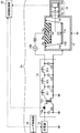
- FIG. 2 shows a configuration example of the laser apparatus shown in FIG.
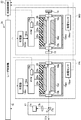
- FIG. 3 shows the configuration of the pulse power module shown in FIG. 2 and the internal configuration of the laser chamber as viewed from a direction substantially parallel to the traveling direction of the laser beam.
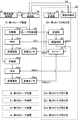
- FIG. 4 is a block diagram showing the configuration of the synchronization control unit shown in FIG. 1 and its surroundings.
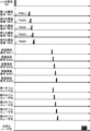
- FIG. 5 is a timing chart in the laser system shown in FIG.
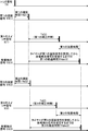
- FIG. 6 is a timing chart of the first and second trigger correction units shown in FIG. FIG.
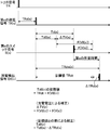
- FIG. 7 is a timing chart showing a specific correction method in the nth trigger correction unit.
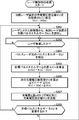
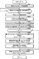
- FIG. 8 is a flowchart showing processing of the laser system control unit shown in FIG.
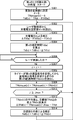
- FIG. 9 is a flowchart showing processing of the laser control unit shown in FIG.
- FIG. 10 is a flowchart showing the processing of the nth trigger correction unit shown in FIG.
- FIG. 11 illustrates a configuration example of a laser apparatus included in the laser system according to the second embodiment of the present disclosure.
- FIG. 12 is a block diagram illustrating a configuration of the synchronization control unit and its periphery in the second embodiment.
- FIG. 13 is a timing chart showing a specific correction method in the nth trigger correction unit of the second embodiment.
- FIG. 14A is a flowchart illustrating processing of the nth trigger correction unit in the second embodiment.
- FIG. 14B is a flowchart illustrating the processing of the nth trigger correction unit in the second embodiment.
- FIG. 15 is a block diagram illustrating a configuration of a laser system according to the third embodiment of the present disclosure.
- FIG. 16 is a block diagram illustrating a configuration of a laser system according to the fourth embodiment of the present disclosure.
- FIG. 17 schematically illustrates a configuration of a laser annealing apparatus 1 including a laser system 5 according to the fifth embodiment of the present disclosure.
- FIG. 18 shows a specific configuration of the pulse waveform measuring instrument 6 shown in FIG.
- FIG. 19 is a flowchart showing the processing of the laser system control unit 20 shown in FIG. FIG.
- FIG. 20 is a flowchart showing details of processing for measuring and controlling the n-th pulse laser beam shown in FIG.
- FIG. 21 is a flowchart showing details of a process for measuring the pulse waveform of the entire first to Nmaxth pulse laser beams shown in FIG.
- FIG. 22 schematically illustrates the configuration of the optical path length adjuster illustrated in FIGS. 1 and 17.
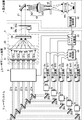
- FIG. 23 shows still another example of the beam forming device.
- FIG. 24 is a block diagram illustrating a schematic configuration of the control unit.
- Laser annealing apparatus including a synchronization control unit (first embodiment) 2.1 Overview of Laser Device 2.2 Beam Luminator 2.3 Exposure Device 2.4 Controller 2.5 Details of Laser Device 2.6 Details of Synchronous Controller 2.7 Timing Chart 2.8 Flowchart 2.8 .1 Processing of laser system control unit 2.8.2 Processing of laser control unit 2.8.3 Processing of nth trigger correction unit Laser system including an amplifier (second embodiment) 3.1 Configuration of Laser Device 3.2 Details of Synchronization Control Unit 3.3 Timing Chart 3.4 Processing of nth Trigger Correction Unit Laser system in which each laser apparatus includes a trigger correction unit 4.1 Third Embodiment 4.2 Fourth Embodiment 5.
- Laser system including pulse waveform measuring instrument (fifth embodiment) 5.1 Configuration 5.2 Pulse waveform measuring instrument 5.3 Control operation Others 6.1 Optical path length adjuster 6.2 Light flux generator using plane mirror 6.3 Configuration of control unit
- Outline A laser annealing apparatus may perform laser annealing by irradiating an amorphous silicon film on a glass substrate with pulsed laser light at a predetermined energy density.
- an increasingly large liquid crystal display is manufactured as in recent years, it may be required to increase the energy per pulse of the pulsed laser light in order to increase the irradiation area at a predetermined energy density.
- the pulse laser beams respectively output from a plurality of laser devices may be converted into light fluxes.
- the amorphous silicon film may be irradiated with a luminous laser beam that has been converted into a luminous flux.
- the first trigger correction unit includes a first switch signal indicating that the first correction time Td (1) has elapsed since the reception of the first delay signal TR (1).
- S (1) may be output.
- the first required time from when the first switch signal S (1) is received to when the first pulse laser beam is generated may vary.
- the first trigger correction unit sets the first correction time Td (1) so that the total time of the first correction time Td (1) and the first required time approaches the target value TRdt. May be.
- the second trigger correction unit outputs a second switch signal S (2) indicating that the second correction time Td (2) has elapsed since the reception of the second delay signal TR (2). Also good.
- the second required time from the time when the second switch signal S (2) is received to the time when the second pulsed laser beam is generated varies separately from the first required time. May be.
- the second trigger correction unit sets the second correction time Td (2) so that the total time of the second correction time Td (2) and the second required time approaches the target value TRdt. May be.
- FIG. 1 schematically shows a configuration of a laser annealing apparatus including a laser system according to the first embodiment of the present disclosure.
- the laser annealing apparatus 1 may include a laser system 5 and an exposure apparatus 4.
- the laser system 5 includes first to fifth laser devices 2a to 2e, high reflection mirrors 30a to 30e, high reflection mirrors 35a to 35e, first to fifth optical path length adjusters 7a to 7e, a light beam
- the conversion apparatus 3 may be included.
- Each of the first to fifth laser devices 2a to 2e may be an excimer laser device using, for example, XeF, XeCl, KrF, or ArF as a laser medium.
- the first to fifth laser devices 2a to 2e may have substantially the same configuration.
- the first to fifth laser devices 2a to 2e may output the first to fifth pulse laser beams 21a to 21e, respectively.
- the first to fifth pulse laser beams 21a to 21e may have an ultraviolet wavelength region.
- the first to fifth optical path length adjusters 7a to 7e may be arranged in the optical paths of the first to fifth pulse laser beams 21a to 21e, respectively.
- the first to fifth optical path length adjusters 7a to 7e are the first to fifth pulse laser beams from the output positions of the first to fifth laser devices 2a to 2e to the emission position of the beam splitter 3, respectively.
- Each optical path length may be adjusted so that the optical path lengths of 21a to 21e are equal to each other.
- the high reflection mirrors 30a to 30e and the high reflection mirrors 35a to 35e may be disposed in the optical paths of the first to fifth pulse laser beams 21a to 21e, respectively.
- the first to fifth pulsed laser beams 21a to 21e may be guided to the beam splitter 3.
- five laser devices are illustrated, but the number of laser devices is not particularly limited, and may be any number of two or more.
- the luminous device 3 may include an incident optical system 33 and a beam combiner 34.
- the incident optical system 33 includes a secondary light source optical system 31 and a condenser optical system 32, and may be designed to constitute Koehler illumination.
- the secondary light source optical system 31 may include first to fifth concave lenses 31a to 31e.
- the first concave lens 31a is an optical path of the first pulse laser beam 21a, and may be disposed between the first optical path length adjuster 7a and the condenser optical system 32.
- the first concave lens 31a may expand the beam width of the first pulse laser beam 21a when transmitting the first pulse laser beam 21a toward the condenser optical system 32.
- the first to fifth concave lenses 31a to 31e may have substantially the same configuration.
- the second concave lens 31b may be disposed in the optical path of the second pulse laser beam 21b.
- the third concave lens 31c may be disposed in the optical path of the third pulse laser beam 21c.
- the fourth concave lens 31d may be disposed in the optical path of the fourth pulse laser beam 21d.
- the fifth concave lens 31e may be disposed in the optical path of the fifth pulse laser beam 21e.
- the first to fifth pulsed laser beams 21a to 21e incident on the first to fifth concave lenses 31a to 31e are laser beams having substantially the same beam shape and substantially the same beam divergence. May be.
- the optical path axes of the first to fifth pulse laser beams 21a to 21e transmitted through the first to fifth concave lenses 31a to 31e may be substantially parallel to each other.
- the “optical path axis” of the pulse laser beam means the central axis of the optical path of the pulse laser beam.
- the first to fifth pulsed laser beams 21a to 21e are incident on substantially the same region on the incident surface of the beam combiner 34, and at respective predetermined incident angles. You may arrange
- the condenser optical system 32 may be an area extending over the optical paths of the first to fifth pulsed laser beams 21a to 21e, and may be disposed at a position between the secondary light source optical system 31 and the beam combiner 34.
- the condenser optical system 32 can transmit the first to fifth pulse laser beams 21 a to 21 e toward the beam combiner 34. At this time, the condenser optical system 32 can change the directions of the optical path axes of the first to fifth pulsed laser beams 21a to 21e to respective predetermined directions.
- the condenser optical system 32 may be arranged so that the position of the front focal plane of the condenser optical system 32 substantially coincides with the position of the focal point of each of the first to fifth concave lenses 31a to 31e. Accordingly, the condenser optical system 32 can collimate the first to fifth pulsed laser beams 21a to 21e transmitted through the first to fifth concave lenses 31a to 31e, respectively, so as to be substantially parallel beams.
- the condenser optical system 32 may be arranged so that the position of the rear focal plane of the condenser optical system 32 substantially coincides with the position of the incident side surface of the beam combiner 34. Accordingly, the condenser optical system 32 can cause the first to fifth pulsed laser beams 21a to 21e to be incident on substantially the same region of the beam combiner 34 at respective predetermined incident angles.
- the condenser optical system 32 is illustrated as including one convex lens, but may include a combination with another convex lens or a concave lens (not illustrated), a concave mirror, or the like.
- the beam combiner 34 may include a diffractive optical element (DOE).
- DOE diffractive optical element
- This diffractive optical element may be one in which grooves having a predetermined shape are formed at predetermined intervals on a substrate that transmits ultraviolet light, such as a synthetic quartz or calcium fluoride substrate.
- the first to fifth pulsed laser beams 21a to 21e whose optical path axes are changed in a predetermined direction by the condenser optical system 32 can enter the beam combiner 34.
- the first to fifth pulsed laser beams 21a to 21e incident on the beam combiner 34 can be emitted from the beam combiner 34 in substantially the same direction. That is, the predetermined direction described above may be a direction in which the first to fifth pulsed laser beams 21a to 21e are coupled by the beam combiner 34.
- a beam combiner 34 for example, a diffractive optical element disclosed in US Patent Application Publication No. 2009/0285076 may be used.
- the first to fifth pulse laser beams 21a to 21e emitted from the beam combiner 34 may enter the exposure apparatus 4 through substantially the same optical path.
- the first to fifth pulsed laser beams 21a to 21e may be converted into a light beam by the light beam generator 3.
- a pulse laser beam in which a plurality of pulse laser beams are bundled may be referred to as a light beam laser beam 21.
- the luminous laser beam 21 may have a pulse energy about five times that of the pulse laser beam output from one laser device.
- “Making the plurality of pulsed laser beams into a luminous flux” may include superposing optical paths of the plurality of pulsed laser beams.
- “pluralizing” a plurality of pulse laser beams may include emitting a plurality of pulse laser beams in close proximity to an optical path, as will be described later with reference to FIG.
- the exposure apparatus 4 may include a high reflection mirror 41, an illumination optical system 42, a mask 43, and a transfer optical system 44.
- the exposure apparatus 4 may form the light beam laser beam 21 emitted from the laser system 5 into a predetermined mask pattern and irradiate the irradiated object P.
- the high reflection mirror 41 may be disposed in the optical path of the light beam laser beam 21 emitted from the laser system 5.
- the high reflection mirror 41 may reflect the light beam laser beam 21 and make it incident on the illumination optical system 42.
- the luminous laser beam 21 incident on the illumination optical system 42 may be substantially parallel light.
- the illumination optical system 42 is an optical path of the light beam laser beam 21 and may be disposed between the high reflection mirror 41 and the mask 43.
- the illumination optical system 42 includes a fly-eye lens 421 and a condenser optical system 422, and may be designed to constitute Koehler illumination.
- the fly-eye lens 421 is an optical path of the light beam laser beam 21 and may be disposed between the high reflection mirror 41 and the condenser optical system 422.
- the fly-eye lens 421 may include a plurality of lenses arranged along the cross section of the light beam laser beam 21. Each of the plurality of lenses may enlarge the beam width of each part of the light flux laser beam 21 when passing the part toward the condenser optical system 422.
- the condenser optical system 422 is an optical path of the light beam laser beam 21 and may be disposed between the fly-eye lens 421 and the mask 43.
- the condenser optical system 422 may illuminate the light beam laser beam 21 emitted from the fly-eye lens 421 toward the mask 43.
- the condenser optical system 422 may be arranged so that the position of the rear focal plane of the condenser optical system 422 substantially coincides with the position of the mask 43. Therefore, the condenser optical system 422 can make the luminous laser beams 21 transmitted through each of the plurality of lenses included in the fly-eye lens 421 enter substantially the same region of the mask 43.
- the condenser optical system 422 is illustrated as including one convex lens, but may include a combination with another convex lens or a concave lens (not illustrated), a concave mirror, or the like.
- the illumination optical system 42 may reduce variations in the light intensity distribution in the beam cross section of the light beam laser beam 21 irradiated on the mask 43.
- the mask 43 may be a slit in which a rectangular opening is formed.
- the opening shape of the slit can constitute a mask pattern of the mask 43.
- the mask pattern of the mask 43 is not limited to a rectangular shape, and may be a pattern having a desired shape.
- the transfer optical system 44 is an optical path of the light beam laser beam 21 and may be disposed between the mask 43 and the irradiated object P.
- the transfer optical system 44 may be arranged so that the position of the image of the mask 43 formed by the transfer optical system 44 substantially coincides with the irradiated position of the irradiated object P. Thereby, the transfer optical system 44 may transfer the mask pattern of the mask 43 irradiated with the light beam laser beam 21 to the irradiated object P.
- the transfer optical system 44 may include one or a plurality of convex lenses.
- the transfer optical system 44 is not limited to one or a plurality of convex lenses, and may include, for example, a combination of a convex lens and a concave lens, a concave mirror, or the like.
- the transfer optical system 44 may be configured by a cylindrical lens that transfers only the short direction of the rectangular mask pattern to the irradiation object P.
- the laser system 5 can output the luminous laser beam 21 having higher pulse energy than the pulse laser beam output from one laser device.
- the laser annealing apparatus 1 can irradiate the irradiated object P with the luminous laser beam 21 with a predetermined pulse energy density required for annealing and a wide irradiation area. And it may be possible to efficiently manufacture a large area liquid crystal display.
- the exposure apparatus 4 may include an exposure apparatus control unit 40.
- the exposure apparatus control unit 40 may perform control such as movement of a stage (not shown) for holding the irradiation object P and replacement of the irradiation object P and the mask 43.
- the exposure apparatus control unit 40 may output a trigger signal TR to the laser system control unit 20.
- the laser system 5 may include a laser system control unit 20 and a synchronization control unit 22.
- the laser system control unit 20 may transmit the trigger signal TR received from the exposure apparatus control unit 40 to the synchronization control unit 22.
- the synchronization control unit 22 Based on the trigger signal TR received from the laser system control unit 20, the synchronization control unit 22 sends the first to fifth switch signals S (1) to S (5) to the first to fifth laser devices 2a to 2a, respectively. 2e may be transmitted.
- the first to fifth laser devices 2a to 2e may output pulsed laser light based on the respective switch signals received from the synchronization control unit 22.
- FIG. 2 shows a configuration example of the laser device shown in FIG.
- the first laser device 2a may include a laser chamber 10, a pair of discharge electrodes 11a and 11b, a charger 12, and a pulse power module (PPM) 13.
- the first laser device 2a may further include a high reflection mirror 14, an output coupling mirror 15, a pulse energy measurement unit 17, and a laser control unit 19.
- the configurations of the second to fifth laser devices 2b to 2e may be the same.
- FIG. 2 shows the internal configuration of the laser chamber 10 as viewed from the direction perpendicular to both the traveling direction of the pulsed laser light 21a and the discharge direction between the pair of discharge electrodes 11a and 11b.
- the laser chamber 10 may be a chamber in which a laser gas as a laser medium containing, for example, argon, krypton, or xenon as a rare gas, neon or helium as a buffer gas, chlorine, fluorine, or the like as a halogen gas is enclosed.
- the pair of electrodes 11a and 11b may be disposed in the laser chamber 10 as electrodes for exciting the laser medium by discharge.
- An opening may be formed in the laser chamber 10, and the opening may be closed by the electrical insulating portion 29.
- the electrode 11a may be supported by the electrical insulating portion 29, and the electrode 11b may be supported by the return plate 10d.
- the return plate 10d may be connected to the inner surface of the laser chamber 10 by wirings 10e and 10f described later with reference to FIG.
- the electrically insulating portion 29 may be embedded with a conductive portion 29a.
- the conductive part 29a may apply a high voltage supplied from the pulse power module 13 to the electrode 11a.
- the charger 12 may be a DC power supply that charges a charging capacitor C0 (described later) in the pulse power module 13 with a predetermined voltage.
- the pulse power module 13 may include a switch 13 a controlled by the laser control unit 19. When the switch 13a is turned from OFF to ON, the pulse power module 13 generates a pulsed high voltage from the electric energy held in the charging capacitor C0, and applies this high voltage between the pair of electrodes 11a and 11b. Also good.
- Windows 10 a and 10 b may be provided at both ends of the laser chamber 10.
- the light generated in the laser chamber 10 can be emitted to the outside of the laser chamber 10 through the windows 10a and 10b.
- the high reflection mirror 14 may reflect the light emitted from the window 10 a of the laser chamber 10 with a high reflectance and return it to the laser chamber 10.
- the output coupling mirror 15 may transmit a part of the light output from the window 10 b of the laser chamber 10 and output it, and may reflect the other part and return it to the laser chamber 10.
- an optical resonator can be configured by the high reflection mirror 14 and the output coupling mirror 15.
- the light emitted from the laser chamber 10 reciprocates between the high reflection mirror 14 and the output coupling mirror 15 and can be amplified every time it passes through the laser gain space between the electrode 11a and the electrode 11b. A part of the amplified light can be output as pulsed laser light 21 a via the output coupling mirror 15.
- the pulse energy measuring unit 17 may be disposed in the optical path of the pulsed laser light 21a output via the output coupling mirror 15.
- the pulse energy measurement unit 17 may include a beam splitter 17a, a condensing optical system 17b, and an optical sensor 17c.
- the beam splitter 17a may transmit the pulse laser beam 21a with a high transmittance and reflect a part of the pulse laser beam 21a toward the condensing optical system 17b.
- the condensing optical system 17b may condense the pulse laser beam reflected by the beam splitter 17a on the light receiving surface of the optical sensor 17c.
- the optical sensor 17 c may detect the pulse energy of the pulsed laser light focused on the light receiving surface and output data of the detected pulse energy to the laser control unit 19.
- the laser control unit 19 may send and receive various signals to and from the laser system control unit 20 described above.
- the laser control unit 19 may receive a trigger signal, target pulse energy data, and the like from the laser system control unit 20. Further, the laser control unit 19 may receive pulse energy data from the pulse energy measurement unit 17.
- the laser control unit 19 controls the set value of the charging voltage of the charger 12 with reference to the target pulse energy data received from the laser system control unit 20 and the pulse energy data received from the pulse energy measurement unit 17. May be.
- the pulse energy of the laser beam may be controlled by controlling the charging voltage of the charger 12.
- FIG. 3 shows the configuration of the pulse power module shown in FIG. 2 and the internal configuration of the laser chamber as viewed from a direction substantially parallel to the traveling direction of the laser beam.
- the conductive member including the wall surface of the laser chamber 10 may be connected to a ground potential.
- the electrode 11b may be connected to the ground potential via the return plate 10d, the wirings 10e and 10f, and the wall surface of the laser chamber 10.
- the first laser device 2 a may include a discharge sensor 18.
- the discharge sensor 18 may include a window 10 c attached to the laser chamber 10, a condensing optical system 181, and an optical sensor 182.
- the discharge sensor 18 may correspond to a discharge timing detector.
- the window 10c may transmit light generated by the discharge between the pair of electrodes 11a and 11b.
- the condensing optical system 181 may condense the light transmitted through the window 10 c on the light receiving surface of the optical sensor 182.
- the optical sensor 182 may include a photodiode or a phototube.
- the optical sensor 182 may transmit a discharge detection signal to the synchronization control unit 22 by detecting light generated by the discharge between the pair of electrodes 11a and 11b.
- the pulse power module 13 includes a charging capacitor C0, a switch 13a, a step-up transformer TC1 as a magnetic compression circuit, a plurality of magnetic switches Sr1 to Sr3, and a plurality of capacitors C1, C2, and C3. Also good.
- any of the magnetic switches Sr1 to Sr3 may include a saturable reactor.
- Each of the magnetic switches Sr1 to Sr3 may have a low impedance when the time integration value of the voltage applied to both ends thereof reaches a predetermined value determined by the characteristics of each magnetic switch.
- the charging voltage V (n) may be set in the charger 12 by the laser control unit 19.
- the charger 12 may charge the charging capacitor C0 based on the set charging voltage V (n).
- a switch signal may be input to the switch 13 a of the pulse power module 13 by the synchronization control unit 22. When the switch signal is input to the switch 13a, the switch 13a may be turned on. When the switch 13a is turned on, a current can flow from the charging capacitor C0 to the primary side of the step-up transformer TC1.
- the magnetic switch Sr1 When the time integral value of the voltage applied to the magnetic switch Sr1 reaches a threshold value, the magnetic switch Sr1 becomes magnetically saturated and the magnetic switch Sr1 can be closed. When the magnetic switch Sr1 is closed, a current flows from the secondary side of the step-up transformer TC1 to the capacitor C1, and the capacitor C1 can be charged.
- the magnetic switch Sr2 When the capacitor C1 is charged, the magnetic switch Sr2 eventually becomes magnetically saturated and the magnetic switch Sr2 can be closed. When the magnetic switch Sr2 is closed, a current flows from the capacitor C1 to the capacitor C2, and the capacitor C2 can be charged. At this time, the capacitor C2 may be charged with a pulse width shorter than the pulse width of the current when the capacitor C1 is charged.
- the magnetic switch Sr3 When the capacitor C2 is charged, the magnetic switch Sr3 eventually becomes magnetically saturated and the magnetic switch Sr3 can be closed. When the magnetic switch Sr3 is closed, a current flows from the capacitor C2 to the capacitor C3, and the capacitor C3 can be charged. At this time, the capacitor C3 may be charged with a pulse width shorter than the pulse width of the current when the capacitor C2 is charged.
- the pulse width of the current can be compressed by sequentially flowing the current from the capacitor C1 to the capacitor C2 and from the capacitor C2 to the capacitor C3.
- the pulse laser beam may be output at a predetermined oscillation frequency.
- an ammeter 18b that detects a discharge current may be used. This ammeter 18b is a current probe, and may detect the timing of discharge.
- an output signal of pulse laser light from the pulse energy measuring unit 17 may be used. The timing signal of the discharge sensor or the output signal of the pulse laser beam may be input to the synchronization control unit 22 described later as a discharge detection signal.
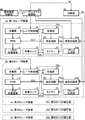
- FIG. 4 is a block diagram showing the configuration of the synchronization control unit shown in FIG. 1 and its surroundings.
- the synchronization control unit 22 may include first to fifth trigger correction units 22a to 22e, a clock generator 23, and a delay circuit unit 24.
- Each of the first to fifth trigger correction units 22a to 22e may include a processing unit 25, a delay circuit 26, and a timer 27.
- FIG. 4 shows the configuration of the first and second trigger correction units 22a and 22b, and the description of the third to fifth trigger correction units 22c to 22e is omitted as appropriate. It's okay.
- each of the first to fifth laser devices 2a to 2e includes a pair of discharge electrodes 11, a charger 12, a pulse power module 13, a discharge sensor 18, and a laser control unit 19. And may be included.
- the configurations of the first and second laser devices 2a and 2b are shown, and the description of the third to fifth laser devices 2c to 2e is omitted as appropriate, but these may be the same. .
- the synchronization control unit 22 receives data of the first delay time TRd (1) of the first delay signal TR (1) from the laser system control unit 20 and the second delay of the second delay signal TR (2). Data of time TRd (2) may be received.
- the clock generator 23 may generate a clock signal common to the first to fifth trigger correction units 22 a to 22 e and the delay circuit unit 24.
- the delay circuit unit 24 may receive the trigger signal TR output from the laser system control unit 20.
- the delay circuit unit 24 receives the first delay signal TR (1) indicating that the first delay time TRd (1) (see FIGS. 5 and 6) has elapsed since the reception of the trigger signal TR. May be output to the delay circuit 26 and the timer 27 of the trigger correction unit 22a.
- the delay circuit unit 24 receives the second delay signal TR (2) indicating that the second delay time TRd (2) (see FIGS. 5 and 6) has elapsed since the reception of the trigger signal TR. May be output to the delay circuit 26 and the timer 27 of the trigger correction unit 22b.
- the delay circuit 26 of the first trigger correction unit 22a is a first that indicates that the first correction time Td (1) (see FIG. 6) has elapsed since the reception of the first delay signal TR (1).
- the switch signal S (1) may be output to the pulse power module 13 of the first laser device 2a.
- the first correction time Td (1) may be set by the processing unit 25 of the first trigger correction unit 22a.
- the delay circuit 26 of the second trigger correction unit 22b is a second that indicates that the second correction time Td (2) (see FIG. 6) has elapsed since the second delay signal TR (2) was received.
- the switch signal S (2) may be output to the pulse power module 13 of the second laser device 2b.
- the second correction time Td (2) may be set by the processing unit 25 of the second trigger correction unit 22b.
- the laser control unit 19 may receive target pulse energy data from the laser system control unit 20.
- the laser control unit 19 may calculate a set value of the charging voltage based on the target pulse energy data.
- the laser control unit 19 may transmit the set value of the charging voltage to the charger 12 and the processing unit 25 of the corresponding trigger correction unit.
- the charger 12 may charge the charging capacitor C0 in the pulse power module 13 according to the set value of the charging voltage.
- the pulse power module 13 may be configured to include the magnetic compression circuit described with reference to FIG.
- the pulse power modules 13 of the first and second laser devices 2a and 2b may receive the first and second switch signals S (1) and S (2) output from the delay circuit 26, respectively. .
- the switch 13a of the pulse power module 13 of the first and second laser devices 2a and 2b may be switched from OFF to ON by switch signals S (1) and S (2), respectively.
- the pulse power module 13 may generate a pulsed high voltage from the electric energy held in the charging capacitor C0. This high voltage may be applied to the pair of discharge electrodes 11.
- the pair of discharge electrodes 11 When a high voltage is applied to the pair of discharge electrodes 11, the pair of discharge electrodes 11 is broken down and discharge may occur.
- the light emitted from the laser medium excited by the energy of the discharge is reciprocated by the above-described optical resonator, whereby pulse laser light can be generated.
- the discharge sensors 18 of the first and second laser devices 2a and 2b detect discharges generated between the pair of discharge electrodes 11, and first and second discharge detection signals DS (1) and DS (2), respectively. May be output.
- the first and second discharge detection signals DS (1) and DS (2) may be input to the timers 27 of the first and second trigger correction units 22a and 22b, respectively.
- the timer 27 of the first trigger correction unit 22a receives a first elapsed time TRdm (from the time when the first delay signal TR (1) is received until the time when the first discharge detection signal DS (1) is received. 1) may be measured and transmitted to the processing unit 25.
- the timer 27 of the second trigger correction unit 22b receives a second elapsed time TRdm (from when the second delay signal TR (2) is received until when the second discharge detection signal DS (2) is received. 2) may be measured and transmitted to the processing unit 25.
- the processing unit 25 of the first trigger correction unit 22a includes the set value of the charging voltage transmitted from the laser control unit 19 of the first laser device 2a and the first elapsed time TRdm (1) transmitted from the timer 27. Based on the above, the first correction time Td (1) may be set.
- the processing unit 25 of the second trigger correction unit 22b includes the set value of the charging voltage transmitted from the laser control unit 19 of the second laser apparatus 2b and the second elapsed time TRdm (2) transmitted from the timer 27. Based on the above, the second correction time Td (2) may be set.
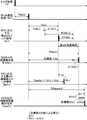
- FIG. 5 is a timing chart in the laser system shown in FIG.
- the laser system control unit 20 may transmit the trigger signal TR received from the exposure apparatus control unit 40 to the synchronization control unit 22.
- the delay circuit unit 24 of the synchronization control unit 22 may output the first to fifth delay signals TR (1) to TR (5) to the first to fifth trigger correction units 22a to 22e, respectively.
- the first to fifth delay signals may each indicate that different first to fifth delay times TRd (1) to TRd (5) have elapsed since the trigger signal TR was received.
- the time from the output timing of the first to fifth delay signals TR (1) to TR (5) to the output timing of the first to fifth discharge detection signals DS (1) to DS (5) is almost equal to each other. It is desirable to be controlled to be equal.
- the first to fifth discharge detection signals DS (1) to DS (5) are output with substantially the same time difference as the time difference between the first to fifth delay signals TR (1) to TR (5). Can be done.
- the first to fifth pulse laser beams 21a to 21e may be output from the first to fifth laser devices 2a to 2e, respectively.
- the first to fifth pulse laser beams 21a to 21e are substantially the same timing as the first to fifth discharge detection signals DS (1) to DS (5), respectively, or the first to fifth discharge detection signals.
- the signals may be output at timing slightly delayed from DS (1) to DS (5).
- the optical path lengths from the respective output positions of the first to fifth laser devices 2a to 2e to the emission position of the beam forming device 3 may be adjusted to be substantially equal to each other as described above.
- the laser beam 21 emitted from the beam splitter 3 has the first to fifth pulses having the same time difference as the time difference between the first to fifth delay signals TR (1) to TR (5).
- the laser beams 21a to 21e may be combined. By controlling the timing of the first to fifth delay signals TR (1) to TR (5), the pulse waveform of the light beam laser beam 21 can be adjusted.
- FIG. 6 is a timing chart of the first and second trigger correction units shown in FIG.
- the third to fifth delay signals TR (3) to TR (5) output from the third to fifth trigger correction units 22c to 22e and the third to fifth laser devices 2c to 2e are output.
- the third to fifth discharge detection signals DS (3) to DS (5) output by are not shown.
- the first delay signal TR (1) and the second delay signal TR (2) may have a predetermined time difference.
- the first required time from the time when the first laser device 2a receives the first switch signal S (1) to the time when the first pulse laser beam is generated is the first laser device 2a. It may vary depending on the charging voltage of the charger 12.
- the second required time from the time when the second laser device 2b receives the second switch signal S (2) to the time when the second pulse laser beam is generated is the charger 12 of the second laser device 2b.
- the charging voltage may vary. These charging voltages can be controlled separately by the first laser device 2a and the second laser device 2b. Accordingly, the first required time and the second required time can vary separately from each other. In addition, the first required time and the second required time can vary depending on the temperature of the magnetic compression circuit included in each pulse power module 13.
- the first elapsed time TRdm (1) from the time when the timer 27 receives the first delay signal TR (1) to the time when the first discharge detection signal DS (1) is received is the first correction time. It may correspond to the total time of Td (1) and the first required time.
- the second elapsed time TRdm (2) from the time when the timer 27 receives the second delay signal TR (2) to the time when the second discharge detection signal DS (2) is received is the second correction time. It may correspond to the total time of Td (2) and the second required time.
- the first pulsed laser beam 21a and the second pulsed laser beam 21b can be generated with substantially the same time difference.
- FIG. 7 is a timing chart showing a specific correction method in the nth trigger correction unit.
- each of the first to fifth trigger correction units 22a to 22e may be referred to as an nth trigger correction unit 22n.
- the signal input or output by the nth trigger correction unit 22n is indicated with (n), or the time set in the nth trigger correction unit 22n is indicated with (n). is there.
- the nth correction time Td (n) may be calculated by the following equation.
- Td (n) Td0 (n) + ⁇ TV (n)
- Td0 (n) may be the first correction element
- ⁇ TV (n) may be the second correction element.
- the initial value of the first correction element Td0 (n) may be set by the following equation.
- Initial value of Td0 (n) TRdt ⁇ F (V0 (n))
- TRdt may be a target value of the nth elapsed time TRdm (n).
- the nth elapsed time TRdm (n) is an elapsed time from when the timer 27 receives the nth delay signal TR (n) to when the timer 27 receives the nth discharge detection signal DS (n). Also good.
- the target value TRdt of the nth elapsed time TRdm (n) is a value common to the first to fifth trigger correction units 22a to 22e will be described, but different target values are set. You may do it.
- F (V0 (n)) is the nth switch signal S (when the value of the charging voltage set in the nth laser device 2n is a predetermined reference voltage value V0 (n). It may be a calculated value of the required time from the input of n) to the output of the nth discharge detection signal DS (n).
- the charging voltage V and the nth switch signal S (n) are input to the switch 13a.
- the product of the required time T until the pulsed high voltage is applied between the discharge electrodes 11 can be a substantially constant value K. Accordingly, the calculation of F (V0 (n)) may be performed by the following equation.
- F (V0 (n)) K / V0 (n) V0 (n) may be a reference voltage value.
- the second correction element ⁇ TV (n) F (V0 (n)) ⁇ F (V (n))
- F (V (n)) is the number from the input of the nth switch signal S (n) when the voltage value of the charging voltage set in the nth laser device 2n is V (n). It may be a calculated value of the time required until n discharge detection signals DS (n) are output.
- the calculation of F (V (n)) may be performed by the following equation.
- F (V (n)) K / V (n)
- the timing control of the nth switch signal S (n) is performed at high speed. Can do.
- the processing unit 25 of the nth trigger correction unit 22n receives the nth discharge detection signal DS (n) from when the timer 27 receives the nth delay signal TR (n).
- the difference ⁇ TRd (n) from the target value TRdt may be calculated.
- the first correction element Td0 (n) may be updated by the following equation.
- Td0 (n) Td0 (n) ⁇ TRd (n)
- the timing control of the nth switch signal S (n) can be performed with high accuracy.
- a change in discharge timing due to a change in temperature of the magnetic compression circuit, a change in gas pressure in the laser chamber, or the like is defined as “drift change”.
- FIG. 8 is a flowchart showing processing of the laser system control unit shown in FIG.
- the laser system control unit 20 performs the following processing on the target pulse energy Et (n) and the nth delay for each of the nth pulse laser beams 21n output from the first to fifth laser apparatuses 2a to 2e.
- the time TRd (n) may be calculated.
- the laser system control unit 20 receives the target pulse waveform data of the light beam laser beam 21 and the target pulse energy data of the light beam laser beam 21 from the exposure device control unit 40 of the exposure apparatus 4. May be.
- the laser system control unit 20 may calculate the target pulse energy Et (n) and the nth delay time TRd (n) for each of the nth pulsed laser beams 21n. For example, when the target pulse waveform of the light beam laser beam 21 has a short pulse width, each of the nth delay times TRd (n) may be a value close to each other.
- the target pulse energy Et (n) of the n-th pulse laser beam 21n is adjusted so that the total of the target pulse energy Et (n) of the n-th pulse laser beam 21n approaches the target pulse energy of the light beam laser beam 21. n) may be determined.
- the laser system control unit 20 may transmit the respective values to the laser control unit 19 of the corresponding laser device. After calculating the nth delay time TRd (n) for each of the nth pulse laser beams 21n, the laser system control unit 20 may transmit these values to the delay circuit unit 24 of the synchronization control unit 22. .
- the laser system control unit 20 may determine whether or not to change the target pulse waveform of the luminous laser beam 21 and the target pulse energy of the luminous laser beam 21. When changing these values (S113; YES), the laser system control unit 20 may return the process to S102 described above. When not changing (S113; NO), the laser system control part 20 may advance a process to S114.
- the laser system control unit 20 may determine whether or not to stop the control of the pulse waveform.
- the laser system control unit 20 may return the process to S113 described above.
- the laser system control unit 20 may end the process of this flowchart.
- the laser system control unit 20 may calculate the target pulse energy Et (n) and the nth delay time TRd (n).
- FIG. 9 is a flowchart showing processing of the laser control unit shown in FIG.
- the laser control unit 19 included in each of the first to fifth laser devices 2a to 2e may calculate the set value V (n) of the charging voltage based on the target pulse energy Et (n) by the following process. Good.
- the laser control unit 19 may set the setting value V (n) of the charging voltage of the laser device 2n to an initial value.
- the initial value of the setting value of the charging voltage may be the above-described reference voltage value V0 (n).
- the laser control unit 19 may read the target pulse energy Et (n) of the laser device 2 (n) from the laser system control unit 20.
- the laser control unit 19 may determine whether or not the laser device 2 (n) oscillates. When the laser device 2 (n) does not oscillate (S203; NO), the laser control unit 19 may stand by until laser oscillation occurs. When the laser apparatus 2 (n) performs laser oscillation (S203; YES), the laser control unit 19 may advance the process to S204.
- the laser control unit 19 may detect the pulse energy E (n) of the pulsed laser light 21n output from the laser device 2n.
- the pulse energy E (n) may be detected by the pulse energy measuring unit 17.
- the laser control unit 19 may calculate a difference ⁇ E (n) between the detected pulse energy E (n) and the target pulse energy Et (n) by the following equation.
- ⁇ E (n) E (n) ⁇ Et (n)
- the laser control unit 19 may calculate the change amount ⁇ V (n) of the set value of the charging voltage based on the difference ⁇ E (n) from the target pulse energy by the following equation.
- ⁇ V (n) H ⁇ ⁇ E (n)
- H may be a proportionality constant.
- the change amount ⁇ V (n) of the set value of the charging voltage may indicate how much the set value of the next charging voltage should be changed.
- the laser control unit 19 may calculate the set value V (n) of the next charging voltage using the following equation.
- V (n) V (n) + ⁇ V (n)
- the laser control unit 19 may transmit the set value V (n) of the next charging voltage to the charger 12 and the processing unit 25 of the nth trigger correction unit 22n.
- the laser control unit 19 may determine whether or not to change the target pulse energy Et (n).
- the laser control unit may return the process to S202 described above.
- the target pulse energy Et (n) is not changed (S208; NO)
- the laser control unit may return the process to S203 described above.
- the laser control unit 19 may calculate the set value V (n) of the charging voltage.
- FIG. 10 is a flowchart showing processing of the nth trigger correction unit shown in FIG.
- the nth trigger correction unit 22n may calculate the first correction element Td0 (n) and the second correction element ⁇ TV (n) constituting the nth correction time Td (n) by the following process. Good.
- J may be a counter for counting the number of oscillation pulses.
- TRdmsum (n) is an nth elapsed time TRdm (n) from the time when the timer 27 receives the nth delay signal TR (n) to the time when the nth discharge detection signal DS (n) is received. It may be a total value of TRdm (n) for calculating an average value.
- Td0 (n) may be a first correction element
- TRdt-F (V0 (n)) may be an initial value of the first correction element described above.
- the nth trigger correction unit 22n may read the set value V (n) of the charging voltage from the laser control unit 19.
- the nth trigger correction unit 22n may calculate the second correction element ⁇ TV (n) by the following equation based on the set value V (n) of the charging voltage.
- ⁇ TV (n) F (V0 (n)) ⁇ F (V (n))
- the nth trigger correction unit 22n may calculate the nth correction time Td (n) by the following equation.
- Td (n) Td0 (n) + ⁇ TV (n)
- Td0 (n) may be a first correction element
- ⁇ TV (n) may be a second correction element.
- the nth trigger correction unit 22n may determine whether or not the nth laser device 2n has oscillated. Whether or not the nth laser device 2n has oscillated may be determined based on whether or not the timer 27 has received the discharge detection signal DS (n) from the discharge sensor 18.
- the nth trigger correction unit 22n may advance the process to S307.
- the n-th trigger correction unit 22n may stand by until the n-th laser device 2n oscillates.
- the nth trigger correction unit 22n may update the value of J by adding 1 to the current value of the counter J.
- the nth trigger correction unit 22n performs the operation from the time when the timer 27 receives the nth delay signal TR (n) to the time when the nth discharge detection signal DS (n) is received.
- the elapsed time TRdm (n) of n may be read from the timer 27.
- the nth trigger correction unit 22n may update the total value TRdmsum (n) of TRdm (n) by the following equation.
- TRdmsum (n) TRdmsum (n) + TRdm (n)
- the nth trigger correction unit 22n may determine whether or not the value of the counter J has reached a predetermined number of samples Jmax. When the value of the counter J has not reached the predetermined number of samples Jmax (S312; NO), the nth trigger correction unit 22n may return the process to S302 described above. When the value of the counter J reaches the predetermined number of samples Jmax (S312; YES), the nth trigger correction unit 22n may advance the process to S313.
- the nth trigger correction unit 22n may calculate a difference ⁇ TRd (n) between the average value of TRdm (n) and the target value TRdt.
- the nth trigger correction unit 22n may update the first correction element Td0 (n) by the following equation.
- Td0 (n) Td0 (n) ⁇ TRd (n)
- the nth trigger correction unit 22n may return the process to S302 described above.
- the nth trigger correction unit 22n calculates the nth correction time Td (n) while updating the first correction element Td0 (n) and the second correction element ⁇ TV (n). May be.
- the second correction element ⁇ TV (n) may be updated for each pulse oscillation as described above.
- the first correction element Td0 (n) may be updated for each pulse oscillation of the predetermined number of samples Jmax.
- the predetermined number of samples Jmax may be, for example, 200 to 10,000 times.
- the frequency of the setting process for setting the nth correction time Td (n) by updating the first correction element Td0 (n) is the nth correction by updating the second correction element ⁇ TV (n). It may be smaller than the frequency of the setting process for setting the time Td (n).
- the nth trigger correction unit 22n corrects the nth correction time Td (n) according to the fluctuation of the nth required time, whereby the nth elapsed time TRdm ( n) can be brought close to the target value TRdt. Specifically, it is possible to control the correction time based on the charging voltage of the charger 12 and to control the correction time according to the fluctuation of the nth required time due to the drift change. Thereby, the discharge timing of each laser device can be stabilized, and the pulse waveform of the light beam laser beam can be stabilized.
- the delay circuit unit 24 controls the pulse waveform of the light beam laser beam by controlling the nth delay time TRd (n), the control is performed separately from the control by the nth trigger correction unit 22n. Can do.
- the clock generator 23 generates a clock signal common to the first to fifth trigger correction units 22 (1) to 22 (5) and the delay circuit unit 24. is doing. Thereby, the mutual error of each delay time TRd (n) or correction time Td (n) can be reduced.
- the electrical signal can be delayed by 1 / c. c may be the speed of light. Therefore, the delay of the signal may be corrected from the length of the electric wire of each switch signal S (n) and the timing signal of each discharge sensor. Further, even if communication is performed using an optical fiber instead of wiring, a similar delay may occur, and this correction may be performed.
- the pulse waveform of the light beam laser beam is controlled by the delay circuit unit 24 controlling the nth delay time TRd (n).
- the present invention is limited to this embodiment.
- the following configuration may be used.
- a distributor that distributes the trigger signal TR from the exposure apparatus control unit 40 without delay is disposed, and different target values TRdt (n) are respectively provided in the trigger correction units 22n corresponding to the laser devices. ) May be set to control the timing of the pulse laser beam output from each laser device.
- the laser system control unit 20, the synchronization control unit 22, and the laser control unit 19 of each laser device control the laser device, but the present disclosure is not limited to this.
- the exposure apparatus control unit 40 included in the exposure apparatus 4 may perform various controls.
- FIG. 11 illustrates a configuration example of a laser device included in a laser system according to the second embodiment of the present disclosure.
- the overall configuration of the laser annealing apparatus 1 may be the same as that shown in FIG.
- the first laser device 2a may include a master oscillator MO and an amplifier PA.
- the configurations of the second to fifth laser devices 2b to 2e may be the same.
- the master oscillator MO may include a laser chamber 10mo, a pair of electrodes 11a and 11b, a charger 12mo, and a pulse power module 13mo.
- the master oscillator MO may further include a high reflection mirror 14, an output coupling mirror 15, and a discharge sensor 18mo.
- the amplifier PA may be disposed in the optical path of the pulsed laser beam output from the master oscillator MO through the output coupling mirror 15.
- the amplifier PA may include a laser chamber 10pa, a pair of electrodes 11a and 11b, a charger 12pa, a pulse power module 13pa, and a discharge sensor 18pa. These configurations may be the same as those included in the master oscillator MO.
- the amplifier PA may not include the high reflection mirror 14 or the output coupling mirror 15.
- the pulsed laser light incident on the window 10a of the amplifier PA may pass through the laser gain space between the electrode 11a and the electrode 11b once and output from the window 10b.
- the laser controller 19 may control the setting value of the charging voltage of the charger 12mo of the master oscillator MO and the setting value of the charging voltage of the charger 12pa of the amplifier PA.
- the pulse energy of the laser beam may be controlled by controlling these charging voltages.
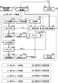
- FIG. 12 is a block diagram showing the configuration of the synchronization control unit and its periphery in the second embodiment.
- the configuration of the first trigger correction unit 22a is shown as the nth trigger correction unit 22n, and description of the second to fifth trigger correction units 22b to 22e is omitted as appropriate. It may be the same.
- the nth trigger correction unit 22n may set the timing of the switch signal for each of the master oscillator MO and the amplifier PA of the nth laser device 2n.
- the delay circuit 26 of the nth trigger correction unit 22n may output the nth switch signal S (n) to the pulse power module 13mo of the master oscillator MO of the nth laser device 2n.
- the nth switch signal S (n) output to the master oscillator MO may be the same as the nth switch signal S (n) described in the first embodiment.
- the delay circuit 26 of the n-th trigger correction unit 22n is supplied to the pulse power module 13pa of the amplifier PA of the n-th laser device 2n, and is different from the n-th switch signal S (n) output to the master oscillator MO.
- Amplifier switch signal Spa (n) may be output.
- the nth amplifier switch signal Spa (n) output to the amplifier PA has passed the nth set time Tdpa (n) since the nth trigger correction unit 22n received the nth delay signal TR (n). It may be a signal indicating that it has been performed.
- the laser control unit 19 may receive target pulse energy data from the laser system control unit 20.
- the laser control unit 19 may calculate a set value of the charging voltage based on the target pulse energy data.
- the laser control unit 19 may transmit the set value of the charging voltage to the charger 12mo, the charger 12pa, and the processing unit 25 of the nth trigger correction unit 22n.
- the setting value of the charging voltage transmitted to the charger 12mo and the charger 12pa is described as being the same value, but may be different from each other.
- the charger 12mo and the charger 12pa may charge the charging capacitor C0 in the pulse power modules 13mo and 13pa, respectively, according to the set value of the charging voltage.
- Each of the pulse power modules 13mo and 13pa may include the magnetic compression circuit described with reference to FIG.
- the pulse power modules 13mo and 13pa of the nth laser apparatus 2n may receive the nth switch signal S (n) and the nth amplifier switch signal Spa (n) output from the delay circuit 26, respectively. .
- Each switch 13a of the pulse power modules 13mo and 13pa may be turned from OFF to ON by these switch signals.
- the pulse power modules 13mo and 13pa may generate respective pulsed high voltages from the electrical energy held in the respective charging capacitors C0 when the respective switches 13a are turned from OFF to ON. A high voltage can be applied between the discharge electrodes 11mo and 11pa, respectively.
- the discharge sensor 18mo of the master oscillator MO may detect a discharge generated between the discharge electrodes 11 of the master oscillator MO and output a discharge detection signal DS (n).
- the discharge sensor 18pa of the amplifier PA may detect a discharge generated between the discharge electrodes 11 of the amplifier PA and output an amplifier discharge detection signal DSpa (n).
- the discharge detection signal DS (n) from the master oscillator MO and the amplifier discharge detection signal DSpa (n) from the amplifier PA may be input to the timer 27.
- the timer 27 of the nth trigger correction unit 22n receives the nth elapsed time from when the nth delay signal TR (n) is received to when the discharge detection signal DS (n) is received from the master oscillator MO.
- TRdm (n) may be measured and transmitted to the processing unit 25.
- the timer 27 of the nth trigger correction unit 22n has a timing difference from when the discharge detection signal DS (n) is received from the master oscillator MO to when the amplifier discharge detection signal DSpa (n) is received from the amplifier PA. Dm (n) may be measured and transmitted to the processing unit 25.
- the processing unit 25 outputs the nth switch to be output to the master oscillator MO based on the set value of the charging voltage transmitted from the laser control unit 19 and the nth elapsed time TRdm (n) transmitted from the timer 27.
- An nth correction time of the signal S (n) may be set.
- the processing unit 25 sets the nth set time Tdpa (n) of the nth amplifier switch signal Spa (n) to be output to the amplifier PA. Also good.
- FIG. 13 is a timing chart showing a specific correction method in the nth trigger correction unit of the second embodiment. Control of the nth switch signal S (n) output to the master oscillator MO may be the same as that described with reference to FIG. 7 in the first embodiment.
- the nth set time Tdpa (n) of the nth amplifier switch signal Spa (n) output to the amplifier PA may be calculated by the following equation.
- Tdpa (n) Td (n) + D (n)
- Td (n) may be the nth correction time of the nth switch signal S (n) output to the master oscillator MO.
- D (n) may be a time difference between the switch signals of the master oscillator MO and the amplifier PA. That is, D (n) is a time difference from the output timing of the nth switch signal S (n) output to the master oscillator MO to the output timing of the nth amplifier switch signal Spa (n) output to the amplifier PA. There may be.
- the timer 27 of the nth trigger correction unit 22n has a timing difference from when the discharge detection signal DS (n) is received from the master oscillator MO to when the amplifier discharge detection signal DSpa (n) is received from the amplifier PA. Dm (n) may be output to the processing unit 25.
- the processing unit 25 of the nth trigger correction unit 22n may calculate a difference ⁇ D (n) from the target value Dt (n).
- the difference ⁇ D (n) may be calculated by the following equation.
- ⁇ D (n) AVG (Dm (n)) ⁇ Dt (n)
- AVG (Dm (n)) may be an average value of the timing difference Dm (n) when the timing difference Dm (n) is measured a plurality of times.
- the target value Dt (n) of the timing difference Dm (n) may be a different value in the first to fifth trigger correction units 22a to 22e.
- the target value Dt (n) may be a value that increases the amplification efficiency in the amplifier PA.
- the time difference D (n) between the switch signals of the master oscillator MO and the amplifier PA may be updated by the following equation.
- D (n) D (n) ⁇ D (n)
- the timing control of the nth amplifier switch signal Spa (n) output to the amplifier PA can be performed with high accuracy.
- FIGS. 14A and 14B are flowcharts showing processing of the nth trigger correction unit in the second embodiment.
- the n-th trigger correction unit 22n performs the following processing, the n-th correction time Td (n) of the n-th switch signal S (n) output to the master oscillator MO, and the switch signal of the master oscillator MO and the amplifier PA.
- the time difference D (n) may be calculated.
- J, TRdmsum (n), and Td0 (n) may be the same as those described in the first embodiment.
- Dsum (n) is a timing difference Dm (n) from when the timer 27 receives the discharge detection signal DS (n) from the master oscillator MO to when it receives the amplifier discharge detection signal DSpa (n) from the amplifier PA.
- D (n) may be a time difference between the switch signals of the master oscillator MO and the amplifier PA.
- Dt (n) may be a target value for the timing difference Dm (n).
- the nth trigger correction unit 22n may determine whether or not the nth laser device 2n has oscillated.
- the n-th trigger correction unit 22n may update the value of J by adding 1 to the current value of the counter J. .
- the nth trigger correction unit 22n starts the discharge detection signal DS from the master oscillator MO from when the timer 27 receives the nth delay signal TR (n).
- the nth elapsed time TRdm (n) until the time (n) is received may be read from the timer 27.
- the nth trigger correction unit 22n may update the total value TRdmsum (n) of TRdm (n) by the following equation.
- TRdmsum (n) TRdmsum (n) + TRdm (n)
- the nth trigger correction unit 22n receives the amplifier discharge detection signal DSpa (n) from the amplifier PA after the timer 27 receives the discharge detection signal DS (n) from the master oscillator MO.
- the timing difference Dm (n) up to this time may be read from the timer 27.
- the nth trigger correction unit 22n may determine whether or not the value of the counter J has reached a predetermined number of samples Jmax. When the value of the counter J has not reached the predetermined number of samples Jmax (S312; NO), the nth trigger correction unit 22n may return the process to S302 described above. When the value of the counter J reaches the predetermined number of samples Jmax (S312; YES), the nth trigger correction unit 22n may advance the process to S313.
- the processing in S313 and the subsequent S314 may be the same as in the first embodiment.
- the nth trigger correction unit 22n may calculate a difference ⁇ D (n) between the average value of the timing differences Dm (n) and the target value Dt (n).
- the nth trigger correction unit 22n may update the time difference D (n) between the switch signals of the master oscillator MO and the amplifier PA by the following equation.
- D (n) D (n) ⁇ D (n)
- the nth trigger correction unit 22n may return the process to S302 described above.
- the nth trigger correction unit 22n performs the nth correction time Td (n) of the nth switch signal S (n) to be output to the master oscillator MO, and switches between the master oscillator MO and the amplifier PA.
- the signal time difference D (n) may be calculated.
- one laser device is not limited to the case where one laser device includes one master oscillator MO and one amplifier PA, and one laser device may include one master oscillator MO and a plurality of amplifiers PA.
- FIG. 15 is a block diagram illustrating a configuration of a laser system according to a third embodiment of the present disclosure.
- the first to fifth trigger correction units 22a to 22e may be included in the first to fifth laser devices 2a to 2e, respectively.
- the laser system 5 may include a distributor 28 instead of the synchronization control unit 22.
- the first to fifth laser devices 2a to 2e may include clock generators 23a to 23e, respectively.
- the clock generators 23c to 23e are not shown.
- the delay circuit unit 24 included in the synchronization control unit 22 the first to fifth laser devices 2a to 2e may include delay circuit units 24a to 24e, respectively. However, illustration of the delay circuit units 24c to 24e is omitted.
- the delay circuit units 24a to 24e included in the first to fifth laser devices 2a to 2e respectively include the delay times TRd (1) to TRd (1) to TR (5) of the first to fifth delay signals TR (1) to TR (5).
- the data of TRd (5) may be received from the laser system control unit 20.
- the distributor 28 receives the trigger signal TR from the laser system control unit 20, and transmits the trigger signal TR to the delay circuit units 24a to 24e included in the first to fifth laser devices 2a to 2e, respectively. Good.
- the delay circuit units 24a to 24e may generate the first to fifth delay signals TR (1) to TR (5) and send them to the first to fifth trigger correction units 22a to 22e, respectively.
- the clock generators 23a to 23e may generate clock signals in the first to fifth laser devices 2a to 2e, respectively.
- the clock signal may be common to the trigger correction unit and the delay circuit unit. Other points may be the same as those in the first embodiment.
- the trigger correction units 22a to 22e and the delay circuit units 24a to 24e are included in the respective laser devices, the wiring distance between the trigger correction unit 22 and the pulse power module 13 is short. Therefore, signal delay due to wiring length can be suppressed.
- the trigger correction units 22a to 22e and the delay circuit units 24a to 24e are included in the respective laser devices is shown, but the present invention is not limited to this example.
- the delay circuit units 24a to 24e are eliminated, and the trigger correction units 22a to 22e are set with different target values TRdt (n), thereby controlling the timing of the pulsed laser light output from each laser device. Also good.
- FIG. 16 is a block diagram illustrating a configuration of a laser system according to a fourth embodiment of the present disclosure.
- the first to fifth trigger correction units 22a to 22e may be included in the first to fifth laser devices 2a to 2e, respectively.
- the laser system 5 may include a distributor 28 instead of the synchronization control unit 22.
- the first to fifth laser devices 2a to 2e may include clock generators 23a to 23e, respectively.
- the clock generators 23b to 23e are not shown.
- the delay circuit unit 24 included in the synchronization control unit 22 the first to fifth laser devices 2a to 2e may include delay circuit units 24a to 24e, respectively. However, illustration of the delay circuit units 24b to 24e is omitted.
- the delay circuit units 24a to 24e included in the first to fifth laser devices 2a to 2e respectively include the delay times TRd (1) to TRd (1) to TR (5) of the first to fifth delay signals TR (1) to TR (5).
- the data of TRd (5) may be received from the laser system control unit 20.
- the distributor 28 receives the trigger signal TR from the laser system control unit 20, and transmits the trigger signal TR to the delay circuit units 24a to 24e included in the first to fifth laser devices 2a to 2e, respectively. Good.
- the delay circuit units 24a to 24e may generate the first to fifth delay signals TR (1) to TR (5) and send them to the first to fifth trigger correction units 22a to 22e, respectively.
- the clock generators 23a to 23e may generate clock signals in the first to fifth laser devices 2a to 2e, respectively.
- the clock signal may be common to the trigger correction unit and the delay circuit unit. Other points may be the same as in the second embodiment.
- the trigger correction units 22a to 22e and the delay circuit units 24a to 24e are included in the respective laser devices, so the trigger correction unit 22 and the pulse power module 13 are included. Since the distance between the wirings becomes short, signal delay due to the wiring length can be suppressed.
- the trigger correction units 22a to 22e and the delay circuit units 24a to 24e are included in the respective laser devices is shown, but the present invention is not limited to this example.
- the delay circuit units 24a to 24e are eliminated, and the trigger correction units 22a to 22e are set with different target values TRdt (n), thereby controlling the timing of the pulsed laser light output from each laser device. Also good.
- FIG. 17 schematically illustrates a configuration of a laser annealing apparatus 1 including a laser system 5 according to the fifth embodiment of the present disclosure.
- the laser system 5 may include a pulse waveform measuring instrument 6 and a shutter 36.
- the pulse waveform measuring device 6 is disposed across the output positions of the first to fifth laser devices 2a to 2e and the optical paths of the first to fifth pulse laser beams 21a to 21e between the beam forming device 3. It may be.
- the first to fifth pulse laser beams 21a to 21e incident on the pulse waveform measuring instrument 6 may be substantially parallel to each other.
- the shutter 36 may be disposed in the vicinity of the optical path of the light beam laser beam 21 output from the light beam generating device 3.
- the shutter 36 may include a shielding plate 36a and an actuator 36b.
- the actuator 36 b may move the shielding plate 36 a in the optical path of the luminous laser beam 21, or retract the shielding plate 36 a from the optical path of the luminous laser beam 21.
- Other points may be the same as those in the first to fourth embodiments.
- FIG. 18 shows a specific configuration of the pulse waveform measuring instrument 6 shown in FIG.
- the pulse waveform measuring instrument 6 may include a beam splitter 61, a condensing optical system 63, an optical sensor 64, and a beam selection mechanism 67.
- the beam splitter 61 may be disposed in the optical path of the first to fifth pulse laser beams 21a to 21e.
- the beam splitter 61 may transmit the first to fifth pulsed laser beams 21a to 21e with high transmittance and reflect a part of each of the first to fifth pulsed laser beams 21a to 21e.
- the beam selection mechanism 67 may include a slit plate 68 and a moving mechanism 69.
- the beam selection mechanism 67 may be positioned in the optical path of the first to fifth pulse laser beams 21a to 21e reflected by the beam splitter 61.
- the moving mechanism 69 may move the slit plate 68 so that the slit plate 68 crosses the optical path axes of the first to fifth pulse laser beams 21a to 21e.
- the slit plate 68 may be formed with a gap having a width that allows only one of the first to fifth pulse laser beams 21a to 21e to pass therethrough.
- all of the first to fifth pulse laser beams 21a to 21e or 1 to 5 included in the first to fifth pulse laser beams 21a to 21e can be selected and passed through the beam selection mechanism 67.
- the condensing optical system 63 can condense all or individual pulse laser beams of the first to fifth pulse laser beams 21 a to 21 e that have passed through the beam selection mechanism 67 on the light receiving surface of the optical sensor 64.
- the optical sensor 64 may be disposed at the position of the focal plane of the condensing optical system 63.
- the photosensor 64 may be a fast response photodiode or phototube.
- the optical sensor 64 may receive the whole of the first to fifth pulse laser beams 21a to 21e or individual pulse laser beams collected by the condensing optical system 63.
- the optical sensor 64 may output the pulse waveform data and the pulse passage timing data of the entire first to fifth pulse laser beams 21a to 21e or individual pulse laser beams to the laser system controller 20. By measuring the entirety of the first to fifth pulse laser beams 21a to 21e, the data may be handled in the same way as the measurement data of the light beam laser beam.
- FIG. 19 is a flowchart showing processing of the laser system control unit 20 shown in FIG.
- the number of laser devices included in the laser system 5 is Nmax.
- the laser system control unit 20 determines the target pulse energy Et (n) of each pulse laser beam and the nth delay time TRd based on the pulse energy and the pulse passing timing for each of the first to Nmaxth pulse laser beams. The correction (n) may be performed. Further, the laser system controller 20 corrects the target pulse energy Et (n) and the nth delay time TRd (n) of each pulsed laser beam based on the pulse waveforms of the entire first to Nmaxth pulsed laser beams. May be performed.
- the laser system control unit 20 may close the shutter 36 and stop the output of the light beam laser beam 21 to the exposure apparatus 4.
- the laser system control unit 20 receives the target pulse waveform data of the light beam laser beam 21 and the target pulse energy data of the light beam laser beam 21 from the exposure device control unit 40 of the exposure device 4. You may receive it. This may be the same as that described with reference to FIG.
- the laser system control unit 20 may calculate the target pulse energy Et (n) and the nth delay time TRd (n) for each of the nth pulsed laser beams 21n. This point may be the same as that described with reference to FIG.
- the laser system control unit 20 may set the value of n to 1.
- the laser system control unit 20 may measure and control the n-th pulse laser beam 21n. For example, when the value of n is 1, measurement and control of the first pulsed laser light 21a may be performed. Details of the process of S105 will be described later with reference to FIG.
- the laser system control unit 20 may determine whether or not the value of n has reached Nmax. If the value of n has not reached Nmax (S106; NO), the laser system control unit 20 adds 1 to the value of n to update the value of n in S107, and returns the process to S105 described above. May be. When the value of n reaches Nmax (S106; YES), the laser system control unit 20 may advance the process to S108.
- the laser system controller 20 may measure the pulse waveform of the entire first to Nmaxth pulse laser beams. Details of the processing of S108 will be described later with reference to FIG.
- the laser system control unit 20 determines whether or not the difference between the pulse waveform of the first to Nmaxth pulse laser beams and the target pulse waveform of the luminous laser beam is within an allowable range. Also good. When the difference from the target pulse waveform is not within the allowable range (S109; NO), the laser system control unit 20 may advance the process to S110. When the difference from the target pulse waveform is within the allowable range (S109; YES), the laser system control unit 20 may advance the process to S112.
- the laser system control unit 20 may close the shutter 36 and stop the output of the light beam laser beam 21 to the exposure apparatus 4. If the shutter 36 has already been closed, the process of S110 may not be executed.
- the laser system control unit 20 may correct the target pulse energy Et (n) and the nth delay time TRd (n) for each of the nth pulsed laser beams 21n. For example, based on the data of the individual pulse laser beams measured in S105, the target pulse energy Et (n) and the nth pulse so that the pulse waveforms of the first to Nmaxth pulse laser beams approach the target pulse waveform. The delay time TRd (n) may be corrected.
- the laser system control unit 20 may return the process to the above-described S104, and perform measurement and control of each pulse laser beam again.
- the laser system control unit 20 may open the shutter 36 and start output of the light beam laser beam 21 to the exposure apparatus 4.
- the laser system control unit 20 may determine whether or not to change the target pulse waveform of the light beam laser beam 21 and the target pulse energy of the beam beam laser beam 21. When these values are changed (S113; YES), the laser system control unit 20 may return the process to S101 described above. When not changing (S113; NO), the laser system control part 20 may advance a process to S114.
- the laser system control unit 20 may determine whether or not to stop the control of the pulse waveform.
- the laser system control unit 20 may return the process to S104 described above.
- the laser system control unit 20 may end the process of this flowchart.
- FIG. 20 is a flowchart showing details of processing for measuring and controlling the n-th pulse laser beam shown in FIG.
- the process shown in FIG. 20 may be performed by the laser system control unit 20 as a subroutine of S105 shown in FIG.
- the laser system control unit 20 may control the beam selection mechanism 67 of the pulse waveform measuring instrument 6 so that the nth pulse laser beam is selected. Thereby, the pulse waveform measuring device 6 may start measuring the pulse waveform of the nth pulse laser beam.
- the laser system control unit 20 may determine whether or not pulse waveform data of k pulses has been acquired. When acquisition of pulse waveform data of k pulses has not been completed (S502; NO), the laser system control unit 20 may wait until acquisition is completed. When the acquisition of the pulse waveform data of k pulses is completed (S502; YES), the laser system control unit 20 may advance the process to S503.
- k is an arbitrary constant for obtaining the average pulse waveform of the nth pulse laser beam.
- the laser system control unit 20 may acquire the average pulse waveform of the nth pulse laser beam from the k pulse waveforms.
- the average pulse waveform may be calculated by calculating the average value of the light intensity at the same time for each time. With the same time, for example, the time when the pulse of the laser beam rises or the peak time of the pulse waveform may be calculated as the same time.
- the laser system control unit 20 may calculate the pulse energy Em (n) of the nth pulse laser beam by integrating the average pulse waveform.
- the laser system control unit 20 may calculate the pulse timing T (n) of the average pulse waveform. For example, an average value of two timings that are half the peak of the average pulse waveform may be set as the pulse timing T (n).
- the laser system control unit 20 may update the nth delay time TRd (n) of the nth pulse laser beam 21n as follows.
- TRd (n) TRd (n) + ⁇ T (n)
- the laser system control unit 20 may advance the process to S511.
- FIG. 21 is a flowchart showing details of a process for measuring the pulse waveform of the entire first to Nmax pulse laser beams shown in FIG.
- the process shown in FIG. 21 may be performed by the laser system control unit 20 as a subroutine of S108 shown in FIG.
- the laser system control unit 20 may control the pulse waveform measuring instrument 6 so that all the first to Nmaxth pulse laser beams are selected. Thereby, the pulse waveform measuring device 6 may start measuring the pulse waveforms of the entire first to Nmaxth pulse laser beams.
- the laser system control unit 20 may determine whether or not the pulse waveform data of k pulses has been acquired. When the acquisition of the pulse waveform data of k pulses has not been completed (S802; NO), the laser system control unit 20 may wait until the acquisition is completed. When the acquisition of the pulse waveform data of k pulses is completed (S802; YES), the laser system control unit 20 may advance the process to S803.
- k is an arbitrary constant for obtaining the average pulse waveform of the entire first to Nmaxth pulse laser beams, and may be the same as or different from k used in S502.
- the laser system control unit 20 may acquire an average pulse waveform from k pulse waveforms.
- the average pulse waveform may be calculated by calculating the average value of the light intensity at the same time for each time. With the same time, for example, the time when the pulse of the laser beam rises or the peak time of the pulse waveform may be calculated as the same time.
- the laser system control unit 20 may integrate the absolute value of the difference between the average pulse waveform and the target pulse waveform.
- the integral value S may be calculated by calculating the absolute value of the difference in light intensity at the same time for each time and calculating the sum of these absolute values.
- the laser system control unit 20 may determine whether or not the integral value S is within an allowable range using the following equation.
- S ⁇ S0 S0 may be a threshold value for determining whether or not it is within an allowable range. If the integral value S is equal to or less than the threshold value S0, it may be determined that it is within the allowable range. When it is within the allowable range (S805; YES), the laser system control unit 20 may advance the process to S806. When the integral value S exceeds the threshold value S0, it may be determined that it is not within the allowable range. If not within the allowable range (S805; NO), the laser system control unit 20 may advance the process to S807.
- the laser system control unit 20 may set the flag F to a value 1 indicating that it is within the allowable range. In S807, the laser system control unit 20 may set the flag F to a value 0 indicating that it is not within the allowable range. After S806 or S807, the laser system control unit 20 may end the process of this flowchart and shift the process to S109 of FIG. The value of the flag F may be used in the determination of S109 shown in FIG.
- the laser system control unit 20 performs the target pulse energy Et (n) and the pulse energy of each pulse laser beam based on the pulse energy and the pulse passing timing for each of the first to Nmaxth pulse laser beams.
- the nth delay time TRd (n) may be corrected.
- the laser system controller 20 corrects the target pulse energy Et (n) and the nth delay time TRd (n) of each pulsed laser beam based on the pulse waveforms of the entire first to Nmaxth pulsed laser beams. May be performed. Thereby, the pulse waveform of the light beam laser beam can be controlled with high accuracy.
- the pulse waveform measuring device 6 includes the beam selection mechanism 67
- the present disclosure is not limited thereto.
- only the nth pulse laser beam 21n is measured, only the nth laser device 2n may oscillate.
- FIG. 22 schematically illustrates the configuration of the optical path length adjuster illustrated in FIGS. 1 and 17.
- the first optical path length adjuster 7a may be a device that can change the optical path length of the first pulse laser beam 21a by bypassing the optical path of the first pulse laser beam 21a.
- the first to fifth optical path length adjusters 7a to 7e may adjust the respective optical path lengths so that the optical path lengths from the respective laser devices to the exit of the laser system 5 substantially coincide with each other.
- the first optical path length adjuster 7a may include a right-angle prism 711, two high reflection mirrors 712 and 713, a plate 714, a plate 715, and a uniaxial stage 716.
- the first surface 701 and the second surface 702 that are orthogonal to the right-angle prism 711 may be coated with a highly reflective film.
- the right-angle prism 711 may be held by a holder 717, and the holder 717 may be fixed to the plate 714.
- the right-angle prism 711 may be located in the optical path of the first pulse laser beam 21a.
- the two high reflection mirrors 712 and 713 may be held by the holder 718 so that their reflection surfaces are orthogonal to each other, and the holder 718 may be fixed to the plate 715.
- the plate 715 may be fixed to the uniaxial stage 716.
- the uniaxial stage 716 may be able to move the two highly reflective mirrors 712 and 713 in parallel with the optical path axis of the first pulse laser beam 21a reflected by the first surface 701 of the right-angle prism 711. .
- the first pulsed laser light 21 a reflected by the first surface 701 of the right-angle prism 711 may be reflected by the two high reflection mirrors 712 and 713 and may enter the second surface 702 of the right-angle prism 711. .
- the first pulse laser beam 21a incident on the second surface 702 of the right-angle prism 711 is an optical path axis that is substantially on the extension line of the optical path axis of the first pulse laser beam 21a incident on the first surface 701 of the right-angle prism 711. , And may exit from the second surface 702 of the right-angle prism 711.
- the laser system control unit 20 may move the two high reflection mirrors 712 and 713 by driving the motor 719 of the single-axis stage 716.
- the optical path length of the first pulse laser beam 21a may be changed by 2X by moving the two high reflection mirrors 712 and 713 by the distance X.
- FIG. 23 shows another example of the light fluxing device.
- the fly-eye lens 421 in the exposure apparatus 4 is also shown, but the high reflection mirror 41 in the exposure apparatus 4 is not shown.
- the beam splitter 37 may include a first right-angle prism 371, a second right-angle prism 372, and a trapezoidal prism 373.
- the first right-angle prism 371 may be formed in a triangular prism shape whose bottom surface, which is a plane parallel to the paper surface, is a right-angle triangle. High reflection films may be coated on two side surfaces of the first right-angle prism 371 forming a right angle. Two side surfaces forming a right angle of the first right-angle prism 371 may constitute a first reflection surface 371a and a second reflection surface 371b, respectively.
- the first right-angle prism 371 may be arranged such that the first reflection surface 371a of the first right-angle prism 371 is parallel to a first reflection surface 373a described later of the trapezoidal prism 373.
- the first right-angle prism 371 may be arranged such that the first reflection surface 371a of the first right-angle prism 371 intersects with the optical path axis of the first pulse laser beam 21a at an angle of 45 °.
- the first right-angle prism 371 may be arranged such that the second reflecting surface 371b of the first right-angle prism 371 intersects with the optical path axis of the second pulse laser beam 21b at an angle of 45 °.
- the second right-angle prism 372 may be formed in a triangular prism shape whose bottom surface, which is a plane parallel to the paper surface, is a right-angle triangle. High reflection films may be coated on two side surfaces of the second right-angle prism 372 forming a right angle. Two side surfaces forming a right angle of the second right-angle prism 372 may constitute a first reflection surface 372a and a second reflection surface 372b, respectively.
- the second right-angle prism 372 may be arranged such that the first reflection surface 372a of the second right-angle prism 372 is parallel to a second reflection surface 373b described later of the trapezoidal prism 373.
- the second right-angle prism 372 may be arranged such that the first reflecting surface 372a of the second right-angle prism 372 intersects with the optical path axis of the fourth pulse laser beam 21d at an angle of 45 °.
- the second right-angle prism 372 may be arranged such that the second reflecting surface 372b of the second right-angle prism 372 intersects with the optical path axis of the fifth pulse laser beam 21e at an angle of 45 °.
- the trapezoidal prism 373 may be formed using a material that transmits ultraviolet rays, such as synthetic quartz or calcium fluoride.
- the trapezoidal prism 373 may be formed in a quadrangular prism shape having a quadrangular bottom surface that is a plane parallel to the paper surface.
- the bottom surface of the trapezoidal prism 373 may be formed in an isosceles trapezoidal shape in which an angle formed by two legs is a right angle.
- Two opposing side surfaces of the trapezoidal prism 373 that are not parallel to each other may be coated with a highly reflective film.
- Two opposing side surfaces of the trapezoidal prism 373 that are not parallel to each other may constitute a first reflecting surface 373a and a second reflecting surface 373b, respectively.
- Two opposing side surfaces of the trapezoidal prism 373 that are parallel to each other may be coated with an antireflection film.
- Two opposite side surfaces of the trapezoidal prism 373 that are parallel to each other may constitute a first irradiation surface 373c and a second irradiation surface 373d.
- the trapezoidal prism 373 may be arranged so that the second irradiation surface 373d of the trapezoidal prism 373 is orthogonal to the optical path axis of the third pulse laser beam 21c.
- the first pulse laser beam 21a output from the first laser device 2a may be reflected by the first reflecting surface 371a of the first right-angle prism 371. Further, the first pulsed laser light 21 a may be reflected by the first reflecting surface 373 a of the trapezoidal prism 373 and incident perpendicularly on the incident side surface of the fly-eye lens 421.
- the second pulse laser beam 21b output from the second laser device 2b may be reflected by the second reflecting surface 371b of the first right-angle prism 371. Further, the second pulse laser beam 21 b may be reflected by the first reflecting surface 373 a of the trapezoidal prism 373 and incident perpendicularly on the incident-side surface of the fly-eye lens 421.
- the third pulse laser beam 21c output from the third laser device 2c may be incident on the second irradiation surface 373d of the trapezoidal prism 373 and go straight inside.
- the third pulse laser beam 21c that travels straight inside the trapezoidal prism 373 may be emitted from the first irradiation surface 373c and perpendicularly incident on the incident-side surface of the fly-eye lens 421.
- the fourth pulse laser beam 21d output from the fourth laser device 2d may be reflected by the first reflecting surface 372a of the second right-angle prism 372. Further, the fourth pulse laser beam 21 d may be reflected by the second reflecting surface 373 b of the trapezoidal prism 373 and incident perpendicularly on the incident side surface of the fly-eye lens 421.
- the fifth pulse laser beam 21e output from the fifth laser device 2e may be reflected by the second reflecting surface 372b of the second right-angle prism 372. Further, the fifth pulsed laser light 21e may be reflected by the second reflecting surface 373b of the trapezoidal prism 373 and incident perpendicularly on the incident-side surface of the fly-eye lens 421.
- the light beam generating device 37 may emit the first to fifth pulse laser beams 21a to 21e as the light beam laser beam 21 so that their optical path axes are parallel to each other. Then, the light beam laser beam 21 emitted from the light beam irradiation device 37 may enter the fly-eye lens 421. That is, the beam splitter 37 may not superimpose the first to fifth pulse laser beams 21a to 21e.
- the pulse waveform measuring device 6 including the beam selection mechanism 67 described with reference to FIG. 18 is provided in the optical path of the beam forming laser beam 21 output from the beam forming device 37. You may arrange.
- FIG. 24 is a block diagram illustrating a schematic configuration of the control unit.
- Control units such as the laser system control unit 20 and the synchronization control unit 22 in the above-described embodiments may be configured by general-purpose control devices such as a computer and a programmable controller. For example, it may be configured as follows.
- the control unit includes a processing unit 1000, a storage memory 1005, a user interface 1010, a parallel I / O controller 1020, a serial I / O controller 1030, A / D, and D / A connected to the processing unit 1000. And a converter 1040. Further, the processing unit 1000 may include a CPU 1001, a memory 1002 connected to the CPU 1001, a timer 1003, and a GPU 1004.
- the processing unit 1000 may read a program stored in the storage memory 1005.
- the processing unit 1000 may execute the read program, read data from the storage memory 1005 in accordance with execution of the program, or store data in the storage memory 1005.
- the parallel I / O controller 1020 may be connected to devices 1021 to 102x that can communicate with each other via a parallel I / O port.
- the parallel I / O controller 1020 may control communication using a digital signal via a parallel I / O port that is performed in the process in which the processing unit 1000 executes a program.
- the serial I / O controller 1030 may be connected to devices 1031 to 103x that can communicate with each other via a serial I / O port.
- the serial I / O controller 1030 may control communication using a digital signal via a serial I / O port that is performed in a process in which the processing unit 1000 executes a program.
- the A / D and D / A converter 1040 may be connected to devices 1041 to 104x that can communicate with each other via an analog port.
- the A / D and D / A converter 1040 may control communication using an analog signal via an analog port that is performed in the process in which the processing unit 1000 executes a program.
- the user interface 1010 may be configured such that the operator displays the execution process of the program by the processing unit 1000, or causes the processing unit 1000 to stop the program execution by the operator or perform interrupt processing.
- the CPU 1001 of the processing unit 1000 may perform arithmetic processing of a program.
- the memory 1002 may temporarily store a program during the course of execution of the program by the CPU 1001 or temporarily store data during a calculation process.
- the timer 1003 may measure time and elapsed time, and output the time and elapsed time to the CPU 1001 according to execution of the program.
- the GPU 1004 may process the image data according to the execution of the program and output the result to the CPU 1001.
- Devices 1021 to 102x that are connected to the parallel I / O controller 1020 and can communicate via the parallel I / O port include first to fifth laser devices 2a to 2e, an exposure device control unit 40, and other control units. For example, it may be used for transmission / reception of an oscillation trigger signal or a signal indicating timing.
- the devices 1031 to 103x that are connected to the serial I / O controller 1030 and can communicate via the serial I / O port include first to fifth laser devices 2a to 2e, an exposure device control unit 40, and other control units. It may be used for data transmission / reception.
- the devices 1041 to 104x connected to the A / D and D / A converter 1040 and capable of communicating via analog ports may be various sensors such as the pulse waveform measuring device 6 and the pulse energy measuring unit 17. With the configuration as described above, the control unit may be able to realize the operation shown in each embodiment.
Landscapes
- Physics & Mathematics (AREA)
- Electromagnetism (AREA)
- Engineering & Computer Science (AREA)
- Optics & Photonics (AREA)
- Plasma & Fusion (AREA)
- Mechanical Engineering (AREA)
- Microelectronics & Electronic Packaging (AREA)
- Lasers (AREA)
- Health & Medical Sciences (AREA)
- Toxicology (AREA)
- Exposure And Positioning Against Photoresist Photosensitive Materials (AREA)
- Automation & Control Theory (AREA)
Abstract
Description
本開示の別の観点に係るレーザシステムは、第1のレーザ装置であって、トリガ信号を受信し、前記トリガ信号を受信した時から第1の遅延時間が経過したことを示す第1の遅延信号を出力する第1の遅延回路部と、前記第1の遅延信号を受信し、前記第1の遅延信号を受信した時から第1の補正時間が経過したことを示す第1のスイッチ信号を出力する第1のトリガ補正部と、前記第1の遅延回路部と、前記第1のトリガ補正部と、に共通のクロック信号を生成する第1のクロック生成器と、第1のコンデンサと、前記第1のコンデンサに電圧を印加する第1の充電器と、前記第1のスイッチ信号を受信して前記第1のコンデンサから電流パルスを生成させる第1のスイッチと、前記第1のコンデンサからの電流パルスを圧縮する第1の磁気圧縮回路と、レーザガスを含む第1のチャンバと、前記第1のチャンバ内に配置され、前記第1の磁気圧縮回路に接続された第1の一対の放電電極と、前記第1の一対の放電電極間での放電を検出して第1の放電検出信号を出力する第1の放電タイミング検出器と、を含む前記第1のレーザ装置と、第2のレーザ装置であって、前記トリガ信号を受信し、前記トリガ信号を受信した時から第2の遅延時間が経過したことを示す第2の遅延信号を出力する第2の遅延回路部と、前記第2の遅延信号を受信し、前記第2の遅延信号を受信した時から第2の補正時間が経過したことを示す第2のスイッチ信号を出力する第2のトリガ補正部と、前記第2の遅延回路部と、前記第2のトリガ補正部と、に共通のクロック信号を生成する第2のクロック生成器と、第2のコンデンサと、前記第2のコンデンサに電圧を印加する第2の充電器と、前記第2のスイッチ信号を受信して前記第2のコンデンサから電流パルスを生成させる第2のスイッチと、前記第2のコンデンサからの電流パルスを圧縮する第2の磁気圧縮回路と、レーザガスを含む第2のチャンバと、前記第2のチャンバ内に配置され、前記第2の磁気圧縮回路に接続された第2の一対の放電電極と、前記第2の一対の放電電極間での放電を検出して第2の放電検出信号を出力する第2の放電タイミング検出器と、を含む前記第2のレーザ装置と、を備え、前記第1のトリガ補正部は、前記第1の放電検出信号を受信し、前記第1の遅延信号を受信してから前記第1の放電検出信号を受信するまでの第1の経過時間が第1の目標値に近づくように前記第1の補正時間を設定し、前記第2のトリガ補正部は、前記第2の放電検出信号を受信し、前記第2の遅延信号を受信してから前記第2の放電検出信号を受信するまでの第2の経過時間が第2の目標値に近づくように前記第2の補正時間を設定してもよい。
1.概要
2.同期制御部を含むレーザアニール装置(第1の実施形態)
2.1 レーザ装置の概要
2.2 光束化装置
2.3 露光装置
2.4 制御部
2.5 レーザ装置の詳細
2.6 同期制御部の詳細
2.7 タイミングチャート
2.8 フローチャート
2.8.1 レーザシステム制御部の処理
2.8.2 レーザ制御部の処理
2.8.3 第nのトリガ補正部の処理
3.増幅器を含むレーザシステム(第2の実施形態)
3.1 レーザ装置の構成
3.2 同期制御部の詳細
3.3 タイミングチャート
3.4 第nのトリガ補正部の処理
4.各レーザ装置がトリガ補正部を含むレーザシステム
4.1 第3の実施形態
4.2 第4の実施形態
5.パルス波形計測器を含むレーザシステム(第5の実施形態)
5.1 構成
5.2 パルス波形計測器
5.3 制御動作
6.その他
6.1 光路長調節器
6.2 平面鏡を用いた光束化装置
6.3 制御部の構成
レーザアニール装置は、ガラス基板上のアモルファスシリコン膜にパルスレーザ光を所定のエネルギー密度で照射することによって、レーザアニールを行ってもよい。近年のようにますます大きな液晶ディスプレイが製造されるようになると、所定のエネルギー密度での照射面積を広げるために、パルスレーザ光の1つのパルスあたりのエネルギーを増加させることが求められ得る。1つのパルスあたりのエネルギーを増加させるために、複数台のレーザ装置からそれぞれ出力されたパルスレーザ光を光束化してもよい。光束化された光束化レーザ光を、アモルファスシリコン膜に照射してもよい。
図1は、本開示の第1の実施形態に係るレーザシステムを含むレーザアニール装置の構成を概略的に示す。レーザアニール装置1は、レーザシステム5と、露光装置4とを備えてもよい。レーザシステム5は、第1~第5のレーザ装置2a~2eと、高反射ミラー30a~30eと、高反射ミラー35a~35eと、第1~第5の光路長調節器7a~7eと、光束化装置3と、を含んでもよい。
第1~第5のレーザ装置2a~2eのそれぞれは、例えば、XeF、XeCl、KrF、又はArFをレーザ媒質とするエキシマレーザ装置であってもよい。第1~第5のレーザ装置2a~2eのそれぞれは、互いに実質的に同一の構成を有してもよい。第1~第5のレーザ装置2a~2eは、それぞれ第1~第5のパルスレーザ光21a~21eを出力してもよい。第1~第5のパルスレーザ光21a~21eは、紫外線の波長領域を有してもよい。
光束化装置3は、入射光学系33と、ビームコンバイナ34と、を備えてもよい。
入射光学系33は、二次光源光学系31と、コンデンサ光学系32とを含み、ケーラー照明を構成するように設計されてもよい。
二次光源光学系31は、第1~第5凹レンズ31a~31eを含んでもよい。
第2凹レンズ31bは、第2のパルスレーザ光21bの光路に配置されてもよい。
第3凹レンズ31cは、第3のパルスレーザ光21cの光路に配置されてもよい。
第4凹レンズ31dは、第4のパルスレーザ光21dの光路に配置されてもよい。
第5凹レンズ31eは、第5のパルスレーザ光21eの光路に配置されてもよい。
第1~第5凹レンズ31a~31eをそれぞれ透過した第1~第5のパルスレーザ光21a~21eの光路軸は、互いにほぼ平行であってもよい。本明細書では、パルスレーザ光の「光路軸」は、パルスレーザ光の光路の中心軸を意味する。
コンデンサ光学系32は、第1~第5のパルスレーザ光21a~21eの光路にまたがる領域であって、二次光源光学系31とビームコンバイナ34との間の位置に配置されてもよい。コンデンサ光学系32は、第1~第5のパルスレーザ光21a~21eを、ビームコンバイナ34に向けて透過させ得る。このとき、コンデンサ光学系32は、第1~第5のパルスレーザ光21a~21eの光路軸の方向を、それぞれの所定方向に変化させ得る。
露光装置4は、高反射ミラー41と、照明光学系42と、マスク43と、転写光学系44とを備えてもよい。露光装置4は、レーザシステム5から出射された光束化レーザ光21を所定のマスクパターンに成形し、被照射物Pに照射してもよい。
以上の構成により、照明光学系42は、マスク43に照射される光束化レーザ光21のビーム断面における光強度分布のばらつきを低減してもよい。
露光装置4は、露光装置制御部40を含んでいてもよい。露光装置制御部40は、被照射物Pを保持するための図示しないステージの移動、被照射物Pやマスク43の交換などの制御を行ってもよい。露光装置制御部40は、レーザシステム制御部20に対し、トリガ信号TRを出力してもよい。
図2は、図1に示されるレーザ装置の構成例を示す。例えば、第1のレーザ装置2aは、レーザチャンバ10と、一対の放電電極11a及び11bと、充電器12と、パルスパワーモジュール(PPM)13と、を含んでもよい。第1のレーザ装置2aは、さらに、高反射ミラー14と、出力結合ミラー15と、パルスエネルギー計測部17と、レーザ制御部19と、を含んでもよい。第2~第5のレーザ装置2b~2eの構成も同様でもよい。図2においては、パルスレーザ光21aの進行方向と一対の放電電極11a及び11b間の放電方向との両方に垂直な方向からみたレーザチャンバ10の内部構成が示されている。
出力結合ミラー15は、レーザチャンバ10のウインドウ10bから出力される光のうちの一部を透過させて出力し、他の一部を反射させてレーザチャンバ10内に戻してもよい。
パルスパワーモジュール13のスイッチ13aには、同期制御部22によりスイッチ信号が入力されてもよい。スイッチ信号がスイッチ13aに入力されると、スイッチ13aがONになってもよい。スイッチ13aがONになると、充電コンデンサC0から昇圧トランスTC1の1次側に電流が流れ得る。
磁気スイッチSr1が閉じると、昇圧トランスTC1の2次側からコンデンサC1に電流が流れ、コンデンサC1が充電され得る。
磁気スイッチSr2が閉じると、コンデンサC1からコンデンサC2に電流が流れ、コンデンサC2が充電され得る。このとき、コンデンサC1を充電する際の電流のパルス幅よりも短いパルス幅で、コンデンサC2が充電されてもよい。
磁気スイッチSr3が閉じると、コンデンサC2からコンデンサC3に電流が流れ、コンデンサC3が充電され得る。このとき、コンデンサC2を充電する際の電流のパルス幅よりも短いパルス幅で、コンデンサC3が充電されてもよい。
また、放電センサの代わりの放電タイミング検出器として、パルスエネルギー計測部17のパルスレーザ光の出力信号を使用してもよい。放電センサのタイミング信号またはパルスレーザ光の出力信号は、放電検出信号として、後述する同期制御部22に入力されてもよい。
図4は、図1に示される同期制御部及びその周辺の構成を示すブロック図である。同期制御部22は、第1~第5のトリガ補正部22a~22eと、クロック生成器23と、遅延回路部24と、を含んでもよい。第1~第5のトリガ補正部22a~22eの各々は、処理部25と、遅延回路26と、タイマー27とを含んでもよい。図4においては、第1及び第2のトリガ補正部22a及び22bの構成を示し、第3~第5のトリガ補正部22c~22eについての説明を適宜省略するが、これらはいずれも同様であってよい。
同期制御部22において、クロック生成器23は、第1~第5のトリガ補正部22a~22eと、遅延回路部24と、に共通のクロック信号を生成してもよい。遅延回路部24は、レーザシステム制御部20から出力されたトリガ信号TRを受信してもよい。遅延回路部24は、トリガ信号TRを受信した時から第1の遅延時間TRd(1)(図5、図6参照)が経過したことを示す第1の遅延信号TR(1)を、第1のトリガ補正部22aの遅延回路26及びタイマー27に出力してもよい。遅延回路部24は、トリガ信号TRを受信した時から第2の遅延時間TRd(2)(図5、図6参照)が経過したことを示す第2の遅延信号TR(2)を、第2のトリガ補正部22bの遅延回路26及びタイマー27に出力してもよい。
第2のトリガ補正部22bの処理部25は、第2のレーザ装置2bのレーザ制御部19から送信された充電電圧の設定値と、タイマー27から送信された第2の経過時間TRdm(2)とに基づいて、第2の補正時間Td(2)を設定してもよい。
図5は、図1に示されるレーザシステムにおけるタイミングチャートである。レーザシステム制御部20は、露光装置制御部40から受信したトリガ信号TRを、同期制御部22に送信してもよい。
同期制御部22の遅延回路部24は、第1~第5のトリガ補正部22a~22eに対し、それぞれ第1~第5の遅延信号TR(1)~TR(5)を出力してもよい。第1~第5の遅延信号は、それぞれ、トリガ信号TRを受信した時から互いに異なる第1~第5の遅延時間TRd(1)~TRd(5)が経過したことを示すものでもよい。
図6においては、第3~第5のトリガ補正部22c~22eが出力する第3~第5の遅延信号TR(3)~TR(5)や、第3~第5のレーザ装置2c~2eが出力する第3~第5の放電検出信号DS(3)~DS(5)の図示は省略されている。
Td(n)=Td0(n)+ΔTV(n)
ここで、Td0(n)を第1の補正要素とし、ΔTV(n)を第2の補正要素としてもよい。
Td0(n)の初期値
=TRdt-F(V0(n))
ここで、TRdtは、第nの経過時間TRdm(n)の目標値であってもよい。第nの経過時間TRdm(n)は、タイマー27が第nの遅延信号TR(n)を受信した時から、第nの放電検出信号DS(n)を受信した時までの経過時間であってもよい。ここでは、第nの経過時間TRdm(n)の目標値TRdtが、第1~第5のトリガ補正部22a~22eに共通の値である場合について説明するが、別々の目標値が設定されるようにしてもよい。
F(V0(n))=K/V0(n)
V0(n)は、基準電圧値でもよい。
ΔTV(n)=F(V0(n))-F(V(n))
ここで、F(V(n))は、第nのレーザ装置2nにおいて設定される充電電圧の電圧値をV(n)とした場合の、第nのスイッチ信号S(n)の入力から第nの放電検出信号DS(n)の出力までの所要時間の計算値であってもよい。F(V(n))の計算は、以下の式で行われてもよい。
F(V(n))=K/V(n)
ΔTRd(n)=AVG(TRdm(n))-TRdt
AVG(TRdm(n))は、TRdm(n)を複数回にわたって計測した場合のTRdm(n)の平均値であってもよい。
Td0(n)=Td0(n)-ΔTRd(n)
2.8.1 レーザシステム制御部の処理
図8は、図1に示されるレーザシステム制御部の処理を示すフローチャートである。レーザシステム制御部20は、以下の処理により、第1~第5のレーザ装置2a~2eから出力される第nのパルスレーザ光21nの各々について、目標パルスエネルギーEt(n)及び第nの遅延時間TRd(n)を算出してもよい。
第nのパルスレーザ光21nの各々について、第nの遅延時間TRd(n)を算出したら、レーザシステム制御部20は、これらの値を同期制御部22の遅延回路部24に送信してもよい。
図9は、図4に示されるレーザ制御部の処理を示すフローチャートである。第1~第5のレーザ装置2a~2eにそれぞれ含まれるレーザ制御部19は、以下の処理により、目標パルスエネルギーEt(n)に基づいて充電電圧の設定値V(n)を算出してもよい。
ΔE(n)=E(n)-Et(n)
ΔV(n)=H・ΔE(n)
ここで、Hは比例定数であってもよい。充電電圧の設定値の変化量ΔV(n)は、次の充電電圧の設定値をどのくらい変化させればよいかを示していてもよい。レーザ制御部19は、次の充電電圧の設定値V(n)を以下の式により算出してもよい。
V(n)=V(n)+ΔV(n)
図10は、図4に示される第nのトリガ補正部の処理を示すフローチャートである。第nのトリガ補正部22nは、以下の処理により、第nの補正時間Td(n)を構成する第1の補正要素Td0(n)及び第2の補正要素ΔTV(n)を算出してもよい。
J=0
TRdmsum(n)=0
Td0(n)=TRdt-F(V0(n))
ここで、Jは発振パルス数を数えるためのカウンタでもよい。TRdmsum(n)は、タイマー27が第nの遅延信号TR(n)を受信した時から、第nの放電検出信号DS(n)を受信した時までの第nの経過時間TRdm(n)の平均値を算出するための、TRdm(n)の合計値であってもよい。Td0(n)は、第1の補正要素であって、TRdt-F(V0(n))は、上述した第1の補正要素の初期値であってもよい。
ΔTV(n)=F(V0(n))-F(V(n))
Td(n)=Td0(n)+ΔTV(n)
ここで、Td0(n)は第1の補正要素であり、ΔTV(n)は第2の補正要素であってもよい。
TRdmsum(n)=TRdmsum(n)+TRdm(n)
ΔTRd(n)=AVG(TRdm(n))-TRdt
=TRdmsum(n)/Jmax-TRdt
Td0(n)=Td0(n)-ΔTRd(n)
なお、同期制御部22と各レーザ装置との配線が長い場合には、配線の長さをlとすると電気信号はl/c遅れ得る。cは光速でもよい。そこで、それぞれのスイッチ信号S(n)とそれぞれの放電センサのタイミング信号の電線の長さから信号の遅れ分を補正してもよい。また、配線の代わりに光ファイバによる通信を行ったとしても同様の遅れが発生し得るので、この補正を行ってもよい。
また、本実施形態では、光束化レーザ光のパルス波形の制御は、遅延回路部24が、第nの遅延時間TRd(n)を制御することにより実現しているが、この実施形態に限定されることなく、以下の構成であってもよい。遅延回路部24の代わりに露光装置制御部40からのトリガ信号TRを遅延することなく分配する分配器を配置し、各レーザ装置に対応するトリガ補正部22nに、それぞれ、異なる目標値TRdt(n)を設定することによって、各レーザ装置から出力されるパルスレーザ光のタイミングを制御してもよい。
3.1 レーザ装置の構成
図11は、本開示の第2の実施形態に係るレーザシステムに含まれるレーザ装置の構成例を示す。レーザアニール装置1の全体的な構成は、図1と同様でよい。
図12は、第2の実施形態における同期制御部及びその周辺の構成を示すブロック図である。図12においては、第1のトリガ補正部22aの構成を第nのトリガ補正部22nとして示し、第2~第5のトリガ補正部22b~22eについての説明を適宜省略するが、これらはいずれも同様であってよい。第2の実施形態において、第nのトリガ補正部22nは、第nのレーザ装置2nのマスターオシレータMOと増幅器PAとのそれぞれについてスイッチ信号のタイミングを設定してもよい。
処理部25は、タイマー27から送信されたタイミング差Dm(n)に基づいて、増幅器PAに出力する第nの増幅器スイッチ信号Spa(n)の第nの設定時間Tdpa(n)を設定してもよい。
図13は、第2の実施形態の第nのトリガ補正部における具体的な補正方法を示すタイミングチャートである。
マスターオシレータMOに出力する第nのスイッチ信号S(n)の制御については、第1の実施形態において図7を参照しながら説明したものと同様でよい。
Tdpa(n)=Td(n)+D(n)
ここで、Td(n)は、マスターオシレータMOに出力する第nのスイッチ信号S(n)の第nの補正時間であってもよい。D(n)は、マスターオシレータMOと増幅器PAのスイッチ信号の時間差であってもよい。すなわち、D(n)は、マスターオシレータMOに出力する第nのスイッチ信号S(n)の出力タイミングから、増幅器PAに出力する第nの増幅器スイッチ信号Spa(n)の出力タイミングまでの時間差であってもよい。
ΔD(n)=AVG(Dm(n))-Dt(n)
AVG(Dm(n))は、タイミング差Dm(n)を複数回にわたって計測した場合のタイミング差Dm(n)の平均値であってもよい。
タイミング差Dm(n)の目標値Dt(n)は、第1~第5のトリガ補正部22a~22eにおいて別々の値であってもよい。目標値Dt(n)は、増幅器PAにおける増幅効率が高くなるような値であってもよい。
D(n)=D(n)-ΔD(n)
図14A及び図14Bは、第2の実施形態における第nのトリガ補正部の処理を示すフローチャートである。第nのトリガ補正部22nは、以下の処理により、マスターオシレータMOに出力する第nのスイッチ信号S(n)の第nの補正時間Td(n)と、マスターオシレータMOと増幅器PAのスイッチ信号の時間差D(n)と、を算出してもよい。
J=0
TRdmsum(n)=0
Td0(n)=TRdt-F(V0(n))
Dsum(n)=0
D(n)=Dt(n)
ここで、Jと、TRdmsum(n)と、Td0(n)とは、第1の実施形態において説明したものと同様でよい。
Dsum(n)は、タイマー27がマスターオシレータMOからの放電検出信号DS(n)を受信した時から増幅器PAからの増幅器放電検出信号DSpa(n)を受信した時までのタイミング差Dm(n)の平均値を算出するための、タイミング差Dm(n)の合計値であってもよい。D(n)は、マスターオシレータMOと増幅器PAのスイッチ信号の時間差であってもよい。Dt(n)は、タイミング差Dm(n)の目標値であってもよい。
次に、S304において、第nのトリガ補正部22nは、マスターオシレータMOに出力する第nのスイッチ信号S(n)の第nの補正時間Td(n)を以下の式により算出してもよい。
Td(n)=Td0(n)+ΔTV(n)
この処理も、第1の実施形態におけるものと同様でよい。
Tdpa(n)=Td(n)+D(n)
次に、S309において、第nのトリガ補正部22nは、以下の式により、TRdm(n)の合計値TRdmsum(n)を更新してもよい。
TRdmsum(n)=TRdmsum(n)+TRdm(n)
これらの処理も、第1の実施形態におけるものと同様でよい。
次に、S311において、第nのトリガ補正部22nは、以下の式により、タイミング差Dm(n)の合計値Dsum(n)を更新してもよい。
Dsum(n)=Dsum(n)+Dm(n)
S313及びその次のS314の処理は、第1の実施形態におけるものと同様でよい。
ΔD(n)=AVG(Dm(n))-Dt(n)
=Dsum(n)/Jmax-Dt(n)
D(n)=D(n)-ΔD(n)
他の点については、第1の実施形態と同様でよい。なお、1つのレーザ装置が1つのマスターオシレータMOと1つの増幅器PAとを含む場合に限らず、1つのレーザ装置が1つのマスターオシレータMOと複数の増幅器PAとを含んでもよい。
4.1 第3の実施形態
図15は、本開示の第3の実施形態に係るレーザシステムの構成を示すブロック図である。第3の実施形態において、第1~第5のトリガ補正部22a~22eは、それぞれ第1~第5のレーザ装置2a~2eに含まれていてもよい。レーザシステム5は、同期制御部22の代わりに、分配器28を含んでもよい。同期制御部22に含まれていたクロック生成器23の代わりに、第1~第5のレーザ装置2a~2eにそれぞれクロック生成器23a~23eが含まれてもよい。但し、クロック生成器23c~23eについては図示を省略している。同期制御部22に含まれていた遅延回路部24の代わりに、第1~第5のレーザ装置2a~2eにそれぞれ遅延回路部24a~24eが含まれてもよい。但し、遅延回路部24c~24eについては図示を省略している。
分配器28は、レーザシステム制御部20からトリガ信号TRを受信し、このトリガ信号TRを、第1~第5のレーザ装置2a~2eにそれぞれ含まれる遅延回路部24a~24eに送信してもよい。遅延回路部24a~24eは、それぞれ、第1~第5の遅延信号TR(1)~TR(5)を生成し、第1~第5のトリガ補正部22a~22eに送信してもよい。クロック生成器23a~23eは、それぞれ、第1~第5のレーザ装置2a~2eにおいてクロック信号を生成してもよい。第1~第5のレーザ装置2a~2eの各々において、クロック信号はトリガ補正部と遅延回路部とに共通であってもよい。
他の点については第1の実施形態と同様でよい。
第3の実施形態では、トリガ補正部22a~22eと遅延回路部24a~24eとがそれぞれのレーザ装置に含まれているので、トリガ補正部22とパルスパワーモジュール13の間の配線の距離が短くなるので、配線の長さによる信号の遅れを抑制し得る。
なお、第3の実施形態では、トリガ補正部22a~22eと遅延回路部24a~24eとがそれぞれのレーザ装置に含まれている場合の例を示したがこの例に限定されることなく、たとえば、遅延回路部24a~24eをなくして、トリガ補正部22a~22eに、それぞれ、異なる目標値TRdt(n)を設定することによって、各レーザ装置から出力されるパルスレーザ光のタイミングを制御してもよい。
図16は、本開示の第4の実施形態に係るレーザシステムの構成を示すブロック図である。第4の実施形態において、第1~第5のトリガ補正部22a~22eは、それぞれ第1~第5のレーザ装置2a~2eに含まれていてもよい。レーザシステム5は、同期制御部22の代わりに、分配器28を含んでもよい。同期制御部22に含まれていたクロック生成器23の代わりに、第1~第5のレーザ装置2a~2eにそれぞれクロック生成器23a~23eが含まれてもよい。但し、クロック生成器23b~23eについては図示を省略している。同期制御部22に含まれていた遅延回路部24の代わりに、第1~第5のレーザ装置2a~2eにそれぞれ遅延回路部24a~24eが含まれてもよい。但し、遅延回路部24b~24eについては図示を省略している。
分配器28は、レーザシステム制御部20からトリガ信号TRを受信し、このトリガ信号TRを、第1~第5のレーザ装置2a~2eにそれぞれ含まれる遅延回路部24a~24eに送信してもよい。遅延回路部24a~24eは、それぞれ、第1~第5の遅延信号TR(1)~TR(5)を生成し、第1~第5のトリガ補正部22a~22eに送信してもよい。クロック生成器23a~23eは、それぞれ、第1~第5のレーザ装置2a~2eにおいてクロック信号を生成してもよい。第1~第5のレーザ装置2a~2eの各々において、クロック信号はトリガ補正部と遅延回路部とに共通であってもよい。
他の点については第2の実施形態と同様でよい。
第3の実施形態と同様に第4の実施形態では、トリガ補正部22a~22eと遅延回路部24a~24eとがそれぞれのレーザ装置に含まれているので、トリガ補正部22とパルスパワーモジュール13の間の配線の距離が短くなるので、配線の長さによる信号の遅れを抑制し得る。
なお、第4の実施形態では、トリガ補正部22a~22eと遅延回路部24a~24eとがそれぞれのレーザ装置に含まれている場合の例を示したがこの例に限定されることなく、たとえば、遅延回路部24a~24eをなくして、トリガ補正部22a~22eに、それぞれ、異なる目標値TRdt(n)を設定することによって、各レーザ装置から出力されるパルスレーザ光のタイミングを制御してもよい。
5.1 構成
図17は、本開示の第5の実施形態に係るレーザシステム5を含むレーザアニール装置1の構成を概略的に示す。第5の実施形態において、レーザシステム5は、パルス波形計測器6と、シャッタ36と、を含んでもよい。
他の点については、第1~第4の実施形態と同様でよい。
図18は、図17に示されるパルス波形計測器6の具体的構成を示す。
パルス波形計測器6は、ビームスプリッタ61と、集光光学系63と、光センサ64と、ビーム選択機構67と、を含んでもよい。
光センサ64は、集光光学系63の焦点面の位置に配置されてもよい。光センサ64は、高速応答のフォトダイオード又は光電管であってもよい。光センサ64は、集光光学系63によって集光された、第1~第5のパルスレーザ光21a~21eの全体又は個々のパルスレーザ光を受光してもよい。光センサ64は、第1~第5のパルスレーザ光21a~21eの全体又は個々のパルスレーザ光のパルス波形のデータ及びパルスの通過タイミングのデータをレーザシステム制御部20に出力してもよい。第1~第5のパルスレーザ光21a~21eの全体を計測することにより、そのデータは光束化レーザ光の計測データと同等に扱われてもよい。
図19は、図17に示されるレーザシステム制御部20の処理を示すフローチャートである。以下の説明において、レーザシステム5に含まれる複数のレーザ装置の数をNmaxとする。レーザシステム制御部20は、第1~第Nmaxのパルスレーザ光のそれぞれについてのパルスエネルギーとパルスの通過タイミングに基づいて、各パルスレーザ光の目標パルスエネルギーEt(n)及び第nの遅延時間TRd(n)の補正を行ってもよい。また、レーザシステム制御部20は、第1~第Nmaxのパルスレーザ光全体のパルス波形に基づいて、各パルスレーザ光の目標パルスエネルギーEt(n)及び第nの遅延時間TRd(n)の補正を行ってもよい。
次に、S105において、レーザシステム制御部20は、第nのパルスレーザ光21nの計測及び制御を行ってもよい。例えば、nの値が1である場合、第1のパルスレーザ光21aの計測及び制御が行われてもよい。S105の処理の詳細については、図20を参照しながら後述する。
次に、S113において、レーザシステム制御部20は、光束化レーザ光21の目標パルス波形と、光束化レーザ光21の目標パルスエネルギーを変更するか否かを判定してもよい。これらの値を変更する場合(S113;YES)、レーザシステム制御部20は、処理を上述のS101に戻してもよい。変更しない場合(S113;NO)、レーザシステム制御部20は、処理をS114に進めてもよい。
次に、S505において、レーザシステム制御部20は、算出されたパルスエネルギーEm(n)とパルスエネルギーの目標値Et(n)との差ΔEm(n)を、以下の式により算出してもよい。
ΔEm(n)=Em(n)-Et(n)
ΔT(n)=T(n)-T(1)
ΔΔT(n)=TRd(n)-TRd(1)-ΔT(n)
TRd(n)=TRd(n)+ΔΔT(n)
S510の後、レーザシステム制御部20は、処理をS511に進めてもよい。
Et(n)=Et(n)+ΔEm(n)
S511の後、レーザシステム制御部20は、本フローチャートの処理を終了して、図19のS106に処理を移行してもよい。
S≦S0
S0は、許容範囲内か否かを判定するための閾値でよい。積分値Sが閾値S0以下であれば、許容範囲内であると判定されてもよい。許容範囲内である場合(S805;YES)、レーザシステム制御部20は、処理をS806に進めてもよい。積分値Sが閾値S0を超えている場合、許容範囲内ではないと判定されてもよい。許容範囲内ではない場合(S805;NO)、レーザシステム制御部20は、処理をS807に進めてもよい。
S807において、レーザシステム制御部20は、フラグFを、許容範囲内ではないことを示す値0にセットしてもよい。
S806又はS807の後、レーザシステム制御部20は、本フローチャートの処理を終了して、図19のS109に処理を移行してもよい。上記のフラグFの値は、図19に示されるS109の判定において用いられてもよい。
6.1 光路長調節器
図22は、図1及び図17に示された光路長調節器の構成を概略的に示す。例えば、第1の光路長調節器7aは、第1のパルスレーザ光21aの光路を迂回させて、第1のパルスレーザ光21aの光路長を変更できる装置でもよい。
第2~第5の光路長調節器7b~7eも、同様でよい。第1~第5の光路長調節器7a~7eは、それぞれのレーザ装置からレーザシステム5の出口までの光路長が略一致するようにそれぞれの光路長を調節してもよい。
直角プリズム711の直交する第1の面701と第2の面702には、高反射膜がコートされていてもよい。直角プリズム711は、ホルダー717に保持され、ホルダー717は、プレート714に固定されていてもよい。直角プリズム711は、第1のパルスレーザ光21aの光路に位置していてもよい。
図23は、光束化装置の別の例を示す。なお、図23においては、露光装置4にあるフライアイレンズ421も示しているが、露光装置4にある高反射ミラー41の図示は省略している。光束化装置37は、第1直角プリズム371と、第2直角プリズム372と、台形プリズム373とを含んでもよい。
図24は、制御部の概略構成を示すブロック図である。
上述した実施の形態におけるレーザシステム制御部20、同期制御部22等の制御部は、コンピュータやプログラマブルコントローラ等汎用の制御機器によって構成されてもよい。例えば、以下のように構成されてもよい。
制御部は、処理部1000と、処理部1000に接続される、ストレージメモリ1005と、ユーザインターフェイス1010と、パラレルI/Oコントローラ1020と、シリアルI/Oコントローラ1030と、A/D、D/Aコンバータ1040とによって構成されてもよい。また、処理部1000は、CPU1001と、CPU1001に接続された、メモリ1002と、タイマー1003と、GPU1004とから構成されてもよい。
処理部1000は、ストレージメモリ1005に記憶されたプログラムを読出してもよい。また、処理部1000は、読出したプログラムを実行したり、プログラムの実行に従ってストレージメモリ1005からデータを読出したり、ストレージメモリ1005にデータを記憶させたりしてもよい。
シリアルI/Oコントローラ1030に接続される、シリアルI/Oポートを介して通信可能な機器1031~103xは、第1~第5のレーザ装置2a~2e、露光装置制御部40、他の制御部等のデータの受送信に使用してもよい。A/D、D/Aコンバータ1040に接続される、アナログポートを介して通信可能な機器1041~104xは、パルス波形計測器6や、パルスエネルギー計測部17等の各種センサであってもよい。
以上のように構成されることで、制御部は各実施形態に示された動作を実現可能であってよい。
Claims (9)
- トリガ信号を受信し、前記トリガ信号を受信した時から第1の遅延時間が経過したことを示す第1の遅延信号と、前記トリガ信号を受信した時から第2の遅延時間が経過したことを示す第2の遅延信号と、を出力する遅延回路部と、
前記第1の遅延信号を受信し、前記第1の遅延信号を受信した時から第1の補正時間が経過したことを示す第1のスイッチ信号を出力する第1のトリガ補正部と、
前記第2の遅延信号を受信し、前記第2の遅延信号を受信した時から第2の補正時間が経過したことを示す第2のスイッチ信号を出力する第2のトリガ補正部と、
第1のレーザ装置であって、第1のコンデンサと、前記第1のコンデンサに電圧を印加する第1の充電器と、前記第1のスイッチ信号を受信して前記第1のコンデンサから電流パルスを生成させる第1のスイッチと、前記第1のコンデンサからの電流パルスを圧縮する第1の磁気圧縮回路と、レーザガスを含む第1のチャンバと、前記第1のチャンバ内に配置され、前記第1の磁気圧縮回路に接続された第1の一対の放電電極と、前記第1の一対の放電電極間での放電を検出して第1の放電検出信号を出力する第1の放電タイミング検出器と、を含む前記第1のレーザ装置と、
第2のレーザ装置であって、第2のコンデンサと、前記第2のコンデンサに電圧を印加する第2の充電器と、前記第2のスイッチ信号を受信して前記第2のコンデンサから電流パルスを生成させる第2のスイッチと、前記第2のコンデンサからの電流パルスを圧縮する第2の磁気圧縮回路と、レーザガスを含む第2のチャンバと、前記第2のチャンバ内に配置され、前記第2の磁気圧縮回路に接続された第2の一対の放電電極と、前記第2の一対の放電電極間での放電を検出して第2の放電検出信号を出力する第2の放電タイミング検出器と、を含む前記第2のレーザ装置と、
前記遅延回路部と、前記第1のトリガ補正部と、前記第2のトリガ補正部と、に共通のクロック信号を生成するクロック生成器と、
を備え、
前記第1のトリガ補正部は、前記第1の放電検出信号を受信し、前記第1の遅延信号を受信してから前記第1の放電検出信号を受信するまでの第1の経過時間が第1の目標値に近づくように前記第1の補正時間を設定し、
前記第2のトリガ補正部は、前記第2の放電検出信号を受信し、前記第2の遅延信号を受信してから前記第2の放電検出信号を受信するまでの第2の経過時間が第2の目標値に近づくように前記第2の補正時間を設定する、
レーザシステム。 - 前記第1のトリガ補正部は、
前記第1の充電器により前記第1のコンデンサに印加される電圧の設定値をさらに受信し、
前記電圧の設定値に基づいて前記第1の補正時間を設定する第1の設定処理と、
前記第1の経過時間に基づいて前記第1の補正時間を設定する第2の設定処理と、を行う、
請求項1記載のレーザシステム。 - 前記第1のトリガ補正部は、
前記第1の設定処理を、第1の頻度で行い、
前記第2の設定処理を、前記第1の頻度より小さい第2の頻度で行う、
請求項2記載のレーザシステム。 - 前記第1のレーザ装置は、前記第1のスイッチ信号を受信して第1のパルスレーザ光を生成する第1の発振器と、前記第1のパルスレーザ光を増幅して出力する第1の増幅器と、を含み、
前記第2のレーザ装置は、前記第2のスイッチ信号を受信して第2のパルスレーザ光を生成する第2の発振器と、前記第2のパルスレーザ光を増幅して出力する第2の増幅器と、を含む、
請求項1記載のレーザシステム。 - 前記第1のトリガ補正部は、前記第1の遅延信号を受信した時から第1の設定時間が経過したことを示す第1の増幅器スイッチ信号をさらに出力し、
前記第1の発振器は、前記第1のコンデンサと、前記第1の充電器と、前記第1のスイッチと、前記第1の磁気圧縮回路と、前記第1のチャンバと、前記第1の一対の放電電極と、前記第1の放電タイミング検出器と、を含み、
前記第1の増幅器は、第3のコンデンサと、前記第3のコンデンサに電圧を印加する第3の充電器と、前記第1の増幅器スイッチ信号を受信して前記第3のコンデンサから電流パルスを生成させる第3のスイッチと、前記第3のコンデンサからの電流パルスを圧縮する第3の磁気圧縮回路と、レーザガスを含む第3のチャンバと、前記第3のチャンバ内に配置され、前記第3の磁気圧縮回路に接続された第3の一対の放電電極と、前記第3の一対の放電電極間での放電を検出して第1の増幅器放電検出信号を出力する第3の放電タイミング検出器と、を含み、
前記第1のトリガ補正部は、前記第1の放電検出信号と前記第1の増幅器放電検出信号とを受信し、前記第1の放電検出信号を受信してから前記第1の増幅器放電検出信号を受信するまでのタイミング差が第3の目標値に近づくように前記第1の設定時間を設定する、
請求項4記載のレーザシステム。 - 第1のレーザ装置であって、
トリガ信号を受信し、前記トリガ信号を受信した時から第1の遅延時間が経過したことを示す第1の遅延信号を出力する第1の遅延回路部と、
前記第1の遅延信号を受信し、前記第1の遅延信号を受信した時から第1の補正時間が経過したことを示す第1のスイッチ信号を出力する第1のトリガ補正部と、
前記第1の遅延回路部と、前記第1のトリガ補正部と、に共通のクロック信号を生成する第1のクロック生成器と、
第1のコンデンサと、前記第1のコンデンサに電圧を印加する第1の充電器と、前記第1のスイッチ信号を受信して前記第1のコンデンサから電流パルスを生成させる第1のスイッチと、前記第1のコンデンサからの電流パルスを圧縮する第1の磁気圧縮回路と、レーザガスを含む第1のチャンバと、前記第1のチャンバ内に配置され、前記第1の磁気圧縮回路に接続された第1の一対の放電電極と、前記第1の一対の放電電極間での放電を検出して第1の放電検出信号を出力する第1の放電タイミング検出器と、
を含む前記第1のレーザ装置と、
第2のレーザ装置であって、
前記トリガ信号を受信し、前記トリガ信号を受信した時から第2の遅延時間が経過したことを示す第2の遅延信号を出力する第2の遅延回路部と、
前記第2の遅延信号を受信し、前記第2の遅延信号を受信した時から第2の補正時間が経過したことを示す第2のスイッチ信号を出力する第2のトリガ補正部と、
前記第2の遅延回路部と、前記第2のトリガ補正部と、に共通のクロック信号を生成する第2のクロック生成器と、
第2のコンデンサと、前記第2のコンデンサに電圧を印加する第2の充電器と、前記第2のスイッチ信号を受信して前記第2のコンデンサから電流パルスを生成させる第2のスイッチと、前記第2のコンデンサからの電流パルスを圧縮する第2の磁気圧縮回路と、レーザガスを含む第2のチャンバと、前記第2のチャンバ内に配置され、前記第2の磁気圧縮回路に接続された第2の一対の放電電極と、前記第2の一対の放電電極間での放電を検出して第2の放電検出信号を出力する第2の放電タイミング検出器と、
を含む前記第2のレーザ装置と、
を備え、
前記第1のトリガ補正部は、前記第1の放電検出信号を受信し、前記第1の遅延信号を受信してから前記第1の放電検出信号を受信するまでの第1の経過時間が第1の目標値に近づくように前記第1の補正時間を設定し、
前記第2のトリガ補正部は、前記第2の放電検出信号を受信し、前記第2の遅延信号を受信してから前記第2の放電検出信号を受信するまでの第2の経過時間が第2の目標値に近づくように前記第2の補正時間を設定する、
レーザシステム。 - 前記第1のレーザ装置から出力されたパルスレーザ光と前記第2のレーザ装置から出力されたパルスレーザ光とを束ねて、光束化レーザ光を出射する光束化装置と、
前記光束化レーザ光のパルス波形を計測するパルス波形計測器と、
をさらに備える、
請求項1記載のレーザシステム。 - 前記遅延回路部は、前記パルス波形計測器によって計測されたパルス波形に基づいて、前記第1の遅延時間及び前記第2の遅延時間を設定する、
請求項7記載のレーザシステム。 - 前記第1のレーザ装置の出力位置から前記光束化装置の出射位置までの第1の光路長と、前記第2のレーザ装置の出力位置から前記光束化装置の出射位置までの第2の光路長との差が小さくなるように前記第1の光路長と前記第2の光路長とを調節する光路長調節器をさらに備え、
前記第1の目標値と前記第2の目標値とが実質的に等しい、
請求項8記載のレーザシステム。
Priority Applications (4)
| Application Number | Priority Date | Filing Date | Title |
|---|---|---|---|
| KR1020167031491A KR102164410B1 (ko) | 2014-06-09 | 2014-11-28 | 레이저 시스템 |
| JP2016527609A JP6436989B2 (ja) | 2014-06-09 | 2014-11-28 | レーザシステム |
| US15/354,670 US9806490B2 (en) | 2014-06-09 | 2016-11-17 | Laser system |
| US15/713,761 US9991665B2 (en) | 2014-06-09 | 2017-09-25 | Laser system |
Applications Claiming Priority (2)
| Application Number | Priority Date | Filing Date | Title |
|---|---|---|---|
| JPPCT/JP2014/065242 | 2014-06-09 | ||
| PCT/JP2014/065242 WO2015189895A1 (ja) | 2014-06-09 | 2014-06-09 | レーザシステム |
Related Child Applications (1)
| Application Number | Title | Priority Date | Filing Date |
|---|---|---|---|
| US15/354,670 Continuation US9806490B2 (en) | 2014-06-09 | 2016-11-17 | Laser system |
Publications (1)
| Publication Number | Publication Date |
|---|---|
| WO2015190012A1 true WO2015190012A1 (ja) | 2015-12-17 |
Family
ID=54833027
Family Applications (2)
| Application Number | Title | Priority Date | Filing Date |
|---|---|---|---|
| PCT/JP2014/065242 Ceased WO2015189895A1 (ja) | 2014-06-09 | 2014-06-09 | レーザシステム |
| PCT/JP2014/081659 Ceased WO2015190012A1 (ja) | 2014-06-09 | 2014-11-28 | レーザシステム |
Family Applications Before (1)
| Application Number | Title | Priority Date | Filing Date |
|---|---|---|---|
| PCT/JP2014/065242 Ceased WO2015189895A1 (ja) | 2014-06-09 | 2014-06-09 | レーザシステム |
Country Status (4)
| Country | Link |
|---|---|
| US (3) | US20170063024A1 (ja) |
| JP (2) | JPWO2015189895A1 (ja) |
| KR (2) | KR20170017883A (ja) |
| WO (2) | WO2015189895A1 (ja) |
Cited By (2)
| Publication number | Priority date | Publication date | Assignee | Title |
|---|---|---|---|---|
| WO2018025394A1 (ja) * | 2016-08-05 | 2018-02-08 | ギガフォトン株式会社 | ガスレーザ装置 |
| US20230017337A1 (en) * | 2019-12-31 | 2023-01-19 | Cymer, Llc | Dual pulsed power system with independent voltage and timing control and reduced power consumption |
Families Citing this family (6)
| Publication number | Priority date | Publication date | Assignee | Title |
|---|---|---|---|---|
| JP6805504B2 (ja) * | 2016-01-13 | 2020-12-23 | 株式会社リコー | 距離測定装置、移動体装置及び距離測定方法 |
| US10596964B2 (en) | 2016-01-13 | 2020-03-24 | Ricoh Company, Ltd. | Distance measurement device, moveable device, and distance measuring method |
| CA3055275A1 (en) * | 2017-03-03 | 2018-09-07 | Furukawa Electric Co., Ltd. | Welding method and welding apparatus |
| KR102630250B1 (ko) * | 2018-10-05 | 2024-01-29 | 엘지이노텍 주식회사 | 깊이 정보를 획득하는 방법 및 카메라 모듈 |
| CN115210970B (zh) * | 2020-03-03 | 2025-09-12 | 西默有限公司 | 用于光源的控制系统 |
| CN116706664A (zh) * | 2023-08-02 | 2023-09-05 | 深圳市中科融光医疗科技有限公司 | 一种高能量时空耦合激光装置及应用方法 |
Citations (6)
| Publication number | Priority date | Publication date | Assignee | Title |
|---|---|---|---|---|
| US20050031004A1 (en) * | 2002-11-05 | 2005-02-10 | Dirk Basting | Excimer or molecular fluorine laser system with precision timing |
| JP2005064184A (ja) * | 2003-08-11 | 2005-03-10 | Komatsu Ltd | 2ステージレーザのパルスエネルギー制御装置及び2ステージレーザシステム |
| JP2009099727A (ja) * | 2007-10-16 | 2009-05-07 | Gigaphoton Inc | 注入同期式放電励起レーザ装置及び注入同期式放電励起レーザ装置における同期制御方法 |
| JP2012019250A (ja) * | 2001-03-21 | 2012-01-26 | Komatsu Ltd | 注入同期式又はmopa方式のレーザ装置 |
| JP2013094845A (ja) * | 2011-11-04 | 2013-05-20 | Towa Corp | レーザ加工装置及びレーザ加工方法 |
| US20130250263A1 (en) * | 2011-06-30 | 2013-09-26 | Anvik Corporation | Pulsed Laser Source with High Repetition Rate |
Family Cites Families (14)
| Publication number | Priority date | Publication date | Assignee | Title |
|---|---|---|---|---|
| JP2000058949A (ja) * | 1998-08-12 | 2000-02-25 | Mitsubishi Electric Corp | レーザ多段増幅装置 |
| US20020071468A1 (en) * | 1999-09-27 | 2002-06-13 | Sandstrom Richard L. | Injection seeded F2 laser with pre-injection filter |
| US6865210B2 (en) | 2001-05-03 | 2005-03-08 | Cymer, Inc. | Timing control for two-chamber gas discharge laser system |
| US20040134894A1 (en) * | 1999-12-28 | 2004-07-15 | Bo Gu | Laser-based system for memory link processing with picosecond lasers |
| JP2002040627A (ja) * | 2000-07-24 | 2002-02-06 | Nec Corp | レーザパターン修正方法並びに修正装置 |
| JP2002280324A (ja) | 2001-03-16 | 2002-09-27 | Sony Corp | レーザ装置 |
| JP4877692B2 (ja) | 2001-03-21 | 2012-02-15 | 株式会社小松製作所 | 注入同期式又はmopa方式のレーザ装置 |
| US7061959B2 (en) | 2001-04-18 | 2006-06-13 | Tcz Gmbh | Laser thin film poly-silicon annealing system |
| JP2004342964A (ja) | 2003-05-19 | 2004-12-02 | Ushio Inc | 高精度同期制御機能を備えた2ステージレーザ装置 |
| US7821900B2 (en) | 2008-05-15 | 2010-10-26 | Northrop Grumman Systems Corporation | Diffractive optical element and method of designing the same |
| DE102008027231B4 (de) | 2008-06-06 | 2016-03-03 | Limo Patentverwaltung Gmbh & Co. Kg | Vorrichtung zur Strahlformung |
| JP5821328B2 (ja) * | 2010-07-26 | 2015-11-24 | セイコーエプソン株式会社 | 電子機器装置、ロボットハンド及びロボット |
| US8238400B2 (en) | 2010-08-09 | 2012-08-07 | Coherent Gmbh | High-precision synchronization of pulsed gas-discharge lasers |
| JP6054028B2 (ja) | 2011-02-09 | 2016-12-27 | ギガフォトン株式会社 | レーザ装置および極端紫外光生成システム |
-
2014
- 2014-06-09 JP JP2016527513A patent/JPWO2015189895A1/ja active Pending
- 2014-06-09 WO PCT/JP2014/065242 patent/WO2015189895A1/ja not_active Ceased
- 2014-06-09 KR KR1020167031490A patent/KR20170017883A/ko not_active Withdrawn
- 2014-11-28 JP JP2016527609A patent/JP6436989B2/ja active Active
- 2014-11-28 KR KR1020167031491A patent/KR102164410B1/ko active Active
- 2014-11-28 WO PCT/JP2014/081659 patent/WO2015190012A1/ja not_active Ceased
-
2016
- 2016-11-14 US US15/350,277 patent/US20170063024A1/en not_active Abandoned
- 2016-11-17 US US15/354,670 patent/US9806490B2/en active Active
-
2017
- 2017-09-25 US US15/713,761 patent/US9991665B2/en active Active
Patent Citations (6)
| Publication number | Priority date | Publication date | Assignee | Title |
|---|---|---|---|---|
| JP2012019250A (ja) * | 2001-03-21 | 2012-01-26 | Komatsu Ltd | 注入同期式又はmopa方式のレーザ装置 |
| US20050031004A1 (en) * | 2002-11-05 | 2005-02-10 | Dirk Basting | Excimer or molecular fluorine laser system with precision timing |
| JP2005064184A (ja) * | 2003-08-11 | 2005-03-10 | Komatsu Ltd | 2ステージレーザのパルスエネルギー制御装置及び2ステージレーザシステム |
| JP2009099727A (ja) * | 2007-10-16 | 2009-05-07 | Gigaphoton Inc | 注入同期式放電励起レーザ装置及び注入同期式放電励起レーザ装置における同期制御方法 |
| US20130250263A1 (en) * | 2011-06-30 | 2013-09-26 | Anvik Corporation | Pulsed Laser Source with High Repetition Rate |
| JP2013094845A (ja) * | 2011-11-04 | 2013-05-20 | Towa Corp | レーザ加工装置及びレーザ加工方法 |
Cited By (5)
| Publication number | Priority date | Publication date | Assignee | Title |
|---|---|---|---|---|
| WO2018025394A1 (ja) * | 2016-08-05 | 2018-02-08 | ギガフォトン株式会社 | ガスレーザ装置 |
| CN109478757A (zh) * | 2016-08-05 | 2019-03-15 | 极光先进雷射株式会社 | 气体激光装置 |
| JPWO2018025394A1 (ja) * | 2016-08-05 | 2019-05-23 | ギガフォトン株式会社 | ガスレーザ装置 |
| CN109478757B (zh) * | 2016-08-05 | 2021-04-16 | 极光先进雷射株式会社 | 气体激光装置 |
| US20230017337A1 (en) * | 2019-12-31 | 2023-01-19 | Cymer, Llc | Dual pulsed power system with independent voltage and timing control and reduced power consumption |
Also Published As
| Publication number | Publication date |
|---|---|
| WO2015189895A1 (ja) | 2015-12-17 |
| US9806490B2 (en) | 2017-10-31 |
| US20170070023A1 (en) | 2017-03-09 |
| JP6436989B2 (ja) | 2018-12-12 |
| KR20170017884A (ko) | 2017-02-15 |
| JPWO2015189895A1 (ja) | 2017-04-20 |
| KR102164410B1 (ko) | 2020-10-12 |
| US20170063024A1 (en) | 2017-03-02 |
| US9991665B2 (en) | 2018-06-05 |
| US20180013258A1 (en) | 2018-01-11 |
| JPWO2015190012A1 (ja) | 2017-04-20 |
| KR20170017883A (ko) | 2017-02-15 |
Similar Documents
| Publication | Publication Date | Title |
|---|---|---|
| JP6436989B2 (ja) | レーザシステム | |
| US10290992B2 (en) | Laser system | |
| US10074958B2 (en) | Laser system | |
| US10050408B2 (en) | Laser system | |
| US9882343B2 (en) | Narrow band laser apparatus | |
| JP6168797B2 (ja) | 極端紫外光生成装置 | |
| US20160087389A1 (en) | Laser system, extreme ultraviolet light generation system, and method of controlling laser apparatus | |
| US20210167568A1 (en) | Gas laser device | |
| US20180173102A1 (en) | Extreme ultraviolet light generation device | |
| WO2017009945A1 (ja) | エキシマレーザ装置 | |
| US9966721B2 (en) | Laser system | |
| RU2339909C1 (ru) | Лазерный дальномер |
Legal Events
| Date | Code | Title | Description |
|---|---|---|---|
| 121 | Ep: the epo has been informed by wipo that ep was designated in this application |
Ref document number: 14894734 Country of ref document: EP Kind code of ref document: A1 |
|
| ENP | Entry into the national phase |
Ref document number: 2016527609 Country of ref document: JP Kind code of ref document: A Ref document number: 20167031491 Country of ref document: KR Kind code of ref document: A |
|
| NENP | Non-entry into the national phase |
Ref country code: DE |
|
| 122 | Ep: pct application non-entry in european phase |
Ref document number: 14894734 Country of ref document: EP Kind code of ref document: A1 |