WO2015182272A1 - 発光装置 - Google Patents
発光装置 Download PDFInfo
- Publication number
- WO2015182272A1 WO2015182272A1 PCT/JP2015/061454 JP2015061454W WO2015182272A1 WO 2015182272 A1 WO2015182272 A1 WO 2015182272A1 JP 2015061454 W JP2015061454 W JP 2015061454W WO 2015182272 A1 WO2015182272 A1 WO 2015182272A1
- Authority
- WO
- WIPO (PCT)
- Prior art keywords
- led chip
- emitting device
- green
- green led
- light emitting
- Prior art date
- Legal status (The legal status is an assumption and is not a legal conclusion. Google has not performed a legal analysis and makes no representation as to the accuracy of the status listed.)
- Ceased
Links
Images






Classifications
-
- H—ELECTRICITY
- H10—SEMICONDUCTOR DEVICES; ELECTRIC SOLID-STATE DEVICES NOT OTHERWISE PROVIDED FOR
- H10W—GENERIC PACKAGES, INTERCONNECTIONS, CONNECTORS OR OTHER CONSTRUCTIONAL DETAILS OF DEVICES COVERED BY CLASS H10
- H10W90/00—Package configurations
-
- H—ELECTRICITY
- H10—SEMICONDUCTOR DEVICES; ELECTRIC SOLID-STATE DEVICES NOT OTHERWISE PROVIDED FOR
- H10H—INORGANIC LIGHT-EMITTING SEMICONDUCTOR DEVICES HAVING POTENTIAL BARRIERS
- H10H20/00—Individual inorganic light-emitting semiconductor devices having potential barriers, e.g. light-emitting diodes [LED]
- H10H20/80—Constructional details
- H10H20/85—Packages
- H10H20/852—Encapsulations
- H10H20/854—Encapsulations characterised by their material, e.g. epoxy or silicone resins
-
- H—ELECTRICITY
- H10—SEMICONDUCTOR DEVICES; ELECTRIC SOLID-STATE DEVICES NOT OTHERWISE PROVIDED FOR
- H10H—INORGANIC LIGHT-EMITTING SEMICONDUCTOR DEVICES HAVING POTENTIAL BARRIERS
- H10H20/00—Individual inorganic light-emitting semiconductor devices having potential barriers, e.g. light-emitting diodes [LED]
- H10H20/80—Constructional details
- H10H20/85—Packages
- H10H20/855—Optical field-shaping means, e.g. lenses
- H10H20/856—Reflecting means
-
- H—ELECTRICITY
- H10—SEMICONDUCTOR DEVICES; ELECTRIC SOLID-STATE DEVICES NOT OTHERWISE PROVIDED FOR
- H10H—INORGANIC LIGHT-EMITTING SEMICONDUCTOR DEVICES HAVING POTENTIAL BARRIERS
- H10H20/00—Individual inorganic light-emitting semiconductor devices having potential barriers, e.g. light-emitting diodes [LED]
- H10H20/80—Constructional details
- H10H20/85—Packages
- H10H20/857—Interconnections, e.g. lead-frames, bond wires or solder balls
-
- H—ELECTRICITY
- H10—SEMICONDUCTOR DEVICES; ELECTRIC SOLID-STATE DEVICES NOT OTHERWISE PROVIDED FOR
- H10W—GENERIC PACKAGES, INTERCONNECTIONS, CONNECTORS OR OTHER CONSTRUCTIONAL DETAILS OF DEVICES COVERED BY CLASS H10
- H10W72/00—Interconnections or connectors in packages
- H10W72/50—Bond wires
- H10W72/541—Dispositions of bond wires
- H10W72/547—Dispositions of multiple bond wires
- H10W72/5473—Dispositions of multiple bond wires multiple bond wires connected to a common bond pad
-
- H—ELECTRICITY
- H10—SEMICONDUCTOR DEVICES; ELECTRIC SOLID-STATE DEVICES NOT OTHERWISE PROVIDED FOR
- H10W—GENERIC PACKAGES, INTERCONNECTIONS, CONNECTORS OR OTHER CONSTRUCTIONAL DETAILS OF DEVICES COVERED BY CLASS H10
- H10W90/00—Package configurations
- H10W90/701—Package configurations characterised by the relative positions of pads or connectors relative to package parts
- H10W90/751—Package configurations characterised by the relative positions of pads or connectors relative to package parts of bond wires
- H10W90/756—Package configurations characterised by the relative positions of pads or connectors relative to package parts of bond wires between a chip and a stacked lead frame, conducting package substrate or heat sink
Definitions
- the present invention relates to a light emitting device using an LED (Light Emitting Diode) chip.
- LED Light Emitting Diode
- Patent Document 1 discloses a light emitting unit block for an image display device that emits basic colors of R (red), G (green), and B (blue), a red light emitting diode element, a blue light emitting diode element, There is disclosed a light emitting unit block that includes at least one yellow-green light-emitting diode element and at least one blue-green light-emitting diode element, and the light-emitting diode elements are arranged close to each other.
- Patent Document 2 describes that the color reproducibility of a display device is improved, and a light emitting module in which a blue light emitting element, a green light emitting element, and a red light emitting phosphor are combined is disclosed. Yes.
- Japanese Patent Publication Japanese Patent Laid-Open No. 10-161567
- Japanese Patent Publication Japanese Patent Publication “JP 2012-69572 A (published April 5, 2012)”
- a green LED chip of a light emitting device has a dominant wavelength range of 520 nm to 530 nm in order to achieve both green color generation during monochromatic light emission and yellow color development due to red and green light emission.
- the color purity of the light emitted by the green LED chip is not so good, and thus, blue-green light by blue and green emission (mixed color) and yellow or yellow-green light by red and green emission (mixed color) are emitted.
- the problem arises that the color purity is not very good.
- the present invention has been made in view of the above problems, and an object thereof is to provide a light-emitting device that can improve the color purity of blue-green light and yellow or yellow-green light. It is in.
- a light-emitting device is a light-emitting device that emits at least blue-green light and yellow or yellow-green light, and includes a substrate and a main surface of the substrate.
- An LED chip group composed of a plurality of LED chips, and a sealing portion that collectively seals the LED chip group.
- the LED chip group includes a first green LED chip and a second green LED chip. And including at least two green LED chips including LED chips, at least one blue LED chip, and at least one red LED chip, wherein the dominant wavelength of the first green LED chip is the second green LED chip. It is characterized by being shorter than the dominant wavelength.
- FIG. 3 is a diagram in which a top view of the light emitting device shown in FIG. 2 is compared with a schematic AA ′ cross-sectional view of the main part thereof. It is a chromaticity diagram showing a color reproduction range of light obtained from the light emitting device.
- FIG. 10 It is a top view of the back surface of the light-emitting device shown in FIG. It is a top view of the light-emitting device which concerns on Embodiment 5 of this invention, and is the figure which abbreviate
- a multi-color light emitting device that can improve color mixing and color purity and greatly widen the color reproduction range by using a plurality of LED chips alone.
- a multi-color light emitting device having RGB LED chips
- at least two green LED chips including a first green LED chip and a second green LED chip, a blue LED chip, and a red LED chip are mounted in one package.
- the dominant wavelength of the 1 green LED chip is set to be relatively shorter than the dominant wavelength of the second green LED chip.
- the dominant wavelength of the first green LED chip is set to 480 nm to 520 nm
- the dominant wavelength of the second green LED chip is set to 530 nm to 560 nm
- the dominant wavelength of the blue LED chip is set to 460 nm to 480 nm
- the dominant of the red LED chip is set.
- the wavelength is preferably 610 nm or more and 630 nm or less.
- the mixed blue-green hue is improved. Further, by mounting the red LED chip and the second green LED chip adjacent to each other, the mixed yellow or yellow-green hue is improved.
- the difference between the dominant wavelength of the longest wavelength green LED chip in the green region and the dominant wavelength of other green LED chips is preferably 20 nm or more.
- the difference between the x value of the longest wavelength green LED chip in the green region and the x value of other green LED chips is 0.06 or more on the xy chromaticity coordinates in the CIE chromaticity diagram.
- FIG. 1 is a top view of the light emitting device according to the present embodiment, and is a view in which illustration of the sealing resin portion is omitted.
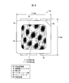
- FIG. 2 is a top view of the light emitting device according to the present embodiment, and is a diagram illustrating a sealing resin portion.
- FIG. 3 is a diagram comparing the top view of the light-emitting device shown in FIG. 2 with the AA ′ schematic cross-sectional view of the main part thereof.
- the light emitting device 100 shown in FIGS. 1 to 3 is a multi-color light emitting device that emits at least blue-green light and yellow or yellow-green light.
- the light emitting device 100 includes a resin reflector 70.
- the resin reflector 70 reflects light.
- the light emitting device 100 includes six outer lead portions 90 including a cathode outer lead and an anode outer lead, an inner lead portion 60, a common inner lead portion 62, an opening portion 80, and an anode mark 95. I have.
- the light emitting device 100 includes a green LED chip (first green LED chip) GB, a green LED chip (second green LED chip) GY, a blue LED chip B, a red LED chip R, a substrate 51, and a sealing resin portion ( Sealing part) 50 is provided.
- the green LED chip GB, the green LED chip GY, the blue LED chip B, and the red LED chip R are LED chip groups surrounded by the resin reflector 70.
- substrate 51 is a part of resin-made reflectors 70 as shown, for example in FIG. 3, and the green LED chip GB, the green LED chip GY, and the blue are on one side (the main surface side of the board 51).
- LED chip B and red LED chip R are arranged.
- the green LED chip GB, the green LED chip GY, the blue LED chip B, and the red LED chip R are arranged in a square shape (here, a rectangle). In the light emitting device 100, the green LED chip is clockwise.
- the green LED chip GB, the green LED chip GY, the blue LED chip B, and the red LED chip R are collectively sealed by one sealing resin portion 50, as shown in FIG.
- a green LED chip GB, a green LED chip GY, a blue LED chip B, and a red LED chip R are arranged inside the opening 80.
- An inner lead portion 60 and a common inner lead portion 62 are formed inside the opening 80.
- the inner lead portion 60 has a chip mounting area equal to or greater than the total number of LED chips (five in FIG. 1 and four in FIG. 8). Further, the green LED chip GB, the green LED chip GY, the blue LED chip B, and the red LED chip R are respectively divided into the same common inner lead part 62 and the corresponding (different) chip mounting areas of the inner lead part 60. It is connected. Each of these connections is made by a bonding wire 40. Each chip mounting area of the inner lead portion 60 and the common inner lead portion 62 are connected to one corresponding outer lead portion 90.
- the size of the light emitting device 100 is 3.2 mm ⁇ 3.5 mm.
- the dominant wavelength of the green LED chip GB is shorter than the dominant wavelength of the green LED chip GY.
- the dominant wavelength means a wavelength obtained by digitizing the color of light emitted from a light emitting element such as an LED as seen by the human eye.
- the dominant wavelength of the green LED chip GB is 480 nm or more and 520 nm or less, and the dominant wavelength of the green LED chip GY is 530 nm or more and 560 nm or less.
- the dominant wavelength of the green LED chip GB can be 504 nm, and the dominant wavelength of the green LED chip GY can be 538 nm or 540 nm.
- the dominant wavelength of the green LED chip GY having the longest dominant wavelength is longer than the dominant wavelength of each of the other green LED chips (here, only the green LED chip GB) by 20 nm or more.
- the dominant wavelength of the blue LED chip B can be set to 465 nm.
- the dominant wavelength of the red LED chip R can be set to 626 nm.
- the green LED chip GB, the green LED chip GY, the blue LED chip B, and the red LED chip R are preferably collected at the center of the main surface of the substrate 51 as much as possible.
- the green LED chip GB is disposed adjacent to the blue LED chip B
- the green LED chip GY is disposed adjacent to the red LED chip R.
- the separation distance between one of the green LED chip GB and the blue LED chip B and one of the green LED chip GY and the red LED chip R is the separation distance between the green LED chip GB and the blue LED chip B and the green LED chip GY. It may be larger than both of the separation distances from the red LED chip R.
- the green LED chip GB By disposing the green LED chip GB adjacent to the blue LED chip B, in the light emitting device 100, the green light and the blue light are mixed well, and a blue-green light with higher color purity is realized. be able to. Further, by arranging the green LED chip GY adjacent to the red LED chip R, in the light emitting device 100, the green light and the red light are mixed with each other more favorably, and the yellow or yellowish green having a high color purity is further obtained. Light can be realized.
- green LED chip GB (dominant wavelength 504 nm), green LED chip GY (dominant wavelength 538 nm), blue LED chip B (dominant wavelength 465 nm), and red LED chip R (dominant wavelength 626 nm) are prepared one by one.
- the adhesive silicone resin was cured at 150 ° C. for 5 hours.
- the green LED chip GB is connected to the corresponding chip mounting area of the common inner lead part 62 and the inner lead part 60 by the bonding wire 40.
- the same connection is performed for the green LED chip GY, the blue LED chip B, and the red LED chip R.
- the common inner lead portion 62 functions as a cathode, and each chip mounting region of the inner lead portion 60 functions as an anode.
- silicone resin is injected into the opening 80 to form the sealing resin portion 50.
- the silicone resin to be injected was first cured at 100 ° C. for 1 hour and then cured at 150 ° C. for 5 hours.
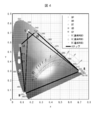
- FIG. 4 is a chromaticity diagram showing the reproduction range of the color of light obtained from the light emitting device.
- the chromaticity diagram shown in FIG. 4 the chromaticity due to light emitted from each LED chip of the light emitting device is plotted on a general CIE chromaticity diagram.
- a point G indicating the chromaticity by light emitted from a normal green LED chip G, a triangle having points B and R as vertices is a chromaticity range of light that can be emitted by a general light emitting device.
- the light emitting device 100 has a blue-green region (x: 0.1, around y: 0.5) and a yellow or yellow-green region (x: 0.25, y: around 0.65) as compared with a general light emitting device. It can be seen that the chromaticity range of
- the difference between the x value of the green LED chip GY with the longest dominant wavelength and the x value of each of the other green LED chips (here, only the green LED chip GB) on the xy chromaticity coordinates in the CIE chromaticity diagram Is preferably 0.06 or more.
- the operating current of the blue LED chip B and the red LED chip R is 20 mA (milliampere)
- the operating current of the green LED chip GB and the green LED chip GY is 10 mA.
- the light emitting device 100 may include at least one protection element that protects at least one LED chip.
- the protection element include a printing resistor or a Zener diode.
- FIG. 5 is a top view of the light emitting device according to the present embodiment, and is a view in which illustration of the sealing resin portion is omitted.
- members having the same functions as those described in any of the above embodiments are denoted by the same reference numerals, and description thereof is omitted.
- the light-emitting device 200 shown in FIG. 5 differs from the light-emitting device 100 shown in FIG. 1 in the following points, and is otherwise substantially the same as the light-emitting device 100 shown in FIG.
- the light emitting device 200 does not include the green LED chip GB, but includes a green LED chip (first green LED chip) BT instead.
- the position of the green LED chip GY and the position of the red LED chip R are opposite to those of the light emitting device 100.
- the green LED chip BT and the green LED chip GY are arranged diagonally, and the blue LED chip B and the red LED chip R are arranged diagonally.
- the dominant wavelength of the green LED chip BT is shorter than the dominant wavelength of the green LED chip GY, and is preferably 480 nm or more and 520 nm or less.
- the dominant wavelength of the green LED chip BT can be 498 nm.
- the dominant wavelength of the green LED chip GY having the longest dominant wavelength is longer than the dominant wavelength of each of the other green LED chips (here, only the green LED chip BT) by 20 nm or more.
- the green LED chip BT (dominant wavelength 498 nm) was fixed to the corresponding chip mounting region of the inner lead portion 60 provided on the main surface side of the substrate 51 with an adhesive silicone resin.
- the adhesive silicone resin was cured at 150 ° C. for 5 hours.
- the green LED chip BT is connected to the corresponding chip mounting areas of the common inner lead part 62 and the inner lead part 60 by the bonding wires 40.
- a point BT indicating chromaticity by light emitted from the green LED chip BT, a square having points GY, B, and R as vertices are chromaticity of light that the light emitting device 200 can emit. It becomes a range. It can be seen that the light emitting device 200 has a wider chromaticity range of blue-green region and yellow or yellow-green region than a general light emitting device.
- the difference between the x value of the green LED chip GY having the longest dominant wavelength and the x value of each of the other green LED chips (here, only the green LED chip BT) on the xy chromaticity coordinates in the CIE chromaticity diagram Is preferably 0.06 or more.
- the light emitting device 200 may include at least one protection element that protects at least one LED chip.
- the protection element include a printing resistor or a Zener diode.
- FIG. 6 is a top view of the light emitting device of the normal example according to the present embodiment, and is a view in which the sealing resin portion is not shown.
- the light-emitting device 300 shown in FIG. 6 is different from the light-emitting device 100 shown in FIG. 1 in the following points, and is otherwise substantially the same as the light-emitting device 100 shown in FIG.
- the light emitting device 300 further includes a green LED chip G.
- the green LED chip G is a green LED chip used in a general light emitting device, and the dominant wavelength is 520 nm or more and 530 nm or less (for example, 525 nm).
- the green LED chip G (dominant wavelength 525 nm) was fixed to the corresponding chip mounting area of the inner lead portion 60 provided on the main surface side of the substrate 51 with an adhesive silicone resin.
- the adhesive silicone resin was cured at 150 ° C. for 5 hours.
- the green LED chip G is also connected to the corresponding chip mounting areas of the common inner lead part 62 and the inner lead part 60 by the bonding wires 40.
- FIG. 7 is a top view of a light emitting device of a modified example according to the present embodiment, and is a view in which illustration of a sealing resin portion is omitted.
- the light emitting device 350 shown in FIG. 7 is different from the light emitting device 300 shown in FIG. 6 in the following points, and is otherwise substantially the same as the light emitting device 300 shown in FIG.
- the position of the green LED chip GB and the position of the blue LED chip B, and the position of the green LED chip GY and the position of the red LED chip R are opposite to the light emitting device 300. It has become.
- a pentagon having a point GB, a point GY, a point B, a point R, and a point G indicating chromaticity due to light emitted from the green LED chip G is a light emitting device 300 and a light emitting device. 350 is the chromaticity range of light that can be emitted. It can be seen that both the light-emitting device 300 and the light-emitting device 350 have a wider chromaticity range in the blue-green region and the yellow or yellow-green region than a general light-emitting device.
- the green LED chip G By further providing the green LED chip G, it is possible to make the appearance of the color of the object more natural during illumination.
- the green LED chip GB, the green LED chip GY, the blue LED chip B, and the red LED chip R are considered as one light emission group
- the color purity of the light emitted by the green LED chip G is the light emitted by the group. Slightly inferior to the color purity of. Therefore, when the green LED chip GB, the green LED chip GY, the blue LED chip B, and the red LED chip R are arranged so as to form a square shape, the green LED chip G is, as shown in FIGS. It is preferable to arrange on the outside of the square shape.
- Both the light emitting device 300 and the light emitting device 350 may include at least one protective element that protects at least one LED chip.
- the protection element include a printing resistor or a Zener diode.
- Table 1 shows the characteristics of the green LED chip GB and the green LED chip GY.
- ⁇ d is the dominant wavelength
- CIE_x is the value of x on the xy chromaticity coordinates in the CIE chromaticity diagram
- CIE_y is the value of y on the same coordinates.
- Table 2 and Table 3 show the characteristics of each LED chip used in each embodiment.
- “t” of the chip size is the height (unit: ⁇ m) of the LED chip.
- the green LED chip BP and the green LED chip BR are not mentioned in the above-described embodiments, but FIG. 4 shows a point BP indicating the chromaticity due to the light emitted by the green LED chip BP. , And a point BR indicating chromaticity due to light emitted from the green LED chip BR.
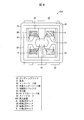
- FIG. 8 is a top view of the light emitting device according to this embodiment, and is a view in which the sealing resin portion is not shown.
- the light-emitting device 400 shown in FIG. 8 differs from the light-emitting device 100 shown in FIG. 1 in the following points, and is otherwise substantially the same as the light-emitting device 100 shown in FIG.
- the light emitting device 400 does not include the inner lead portion 60 and the common inner lead portion 62 but includes the inner lead portion 65 and the common inner lead portion 67 instead. Further, the number of outer lead portions 90 of the light emitting device 400 is four, which is two less than the number of outer lead portions 90 of the light emitting device 100. On the other hand, the light emitting device 400 includes an outer lead portion 96 having a size larger than that of the outer lead portion 90 on the upper right side of FIG. In the light emitting device 400, the blue LED chip B, the green LED chip GY, the red LED chip R, and the green LED chip GB are arranged in the clockwise direction.
- the common inner lead portion 67 has a T shape. Although the number of chip mounting areas of the inner lead portion 60 is five, the number of chip mounting areas of the inner lead portion 65 is four. The chip mounting area on the upper right side of FIG. 8 is connected to the outer lead portion 96.
- the blue LED chip B is connected to the outer lead portion 96 in consideration of the heat dissipation of the blue LED chip B.
- the green LED chip GY and the green LED chip GB are diagonally arranged. Thereby, in the light-emitting device 400, high heat dissipation is realizable.
- the configurations of the inner lead portion, the common inner lead portion, and the outer lead are not limited to those shown in the light emitting device 100.
- the light emitting device 400 may include at least one protection element that protects at least one LED chip.
- the protection element include a printing resistor or a Zener diode.
- the number of LED chips constituting the LED chip group may be four as in the light emitting device 100 or the like, may be five as in the light emitting device 300 or the like, or may be six or more. There may be. In other words, the number of at least one of the green LED chip, the blue LED chip, and the red LED chip may be increased. However, when the number of LED chips constituting the LED chip group is too large, the cost is increased, so care must be taken.
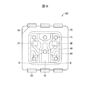
- FIG. 9 is a plan view of the back surface 100 ′ of the light emitting device 100 shown in FIG.
- each member on the main surface of the substrate 51 shown in FIG. 1 that cannot be visually seen in FIG. 9 is indicated by a broken line.
- a through-hole 75 is provided on the back surface 100 ′ of the light emitting device 100 to provide an inner lead 60. It is necessary to suppress the height deviation.
- the through-hole 75 is provided corresponding to each chip mounting area of the inner lead portion 60, penetrates the resin reflector 70, and reaches the back surface of the corresponding chip mounting area.
- the through hole 75 is provided to align the height of the upper surface of the inner lead portion 60 and prevent the height of the inner lead portion 60 from shifting.
- the light emitting device 100 Since a plurality of LED chips are provided in the light emitting device 100, if the height of the upper surface of the inner lead part 60 is uniform, it becomes easy to reduce die bond defects. Further, the green LED chip GB, the green LED chip GY, the blue LED chip B, and the red LED chip R are commonly wire-bonded to the common inner lead part 62, but this also makes it easy to reduce bonding defects. It becomes. This configuration is convenient when the inner lead portion 60 has a plurality of chip mounting areas (the number of wire bonding locations increases). With this configuration, in the light emitting device 100, the color purity due to the color mixture of the light emitted from the adjacent LED chips is improved, and further, the color reproduction range can be expanded.
- a through hole 75 may be provided on the back surface of the light emitting devices 200, 300, 350, 400, 500 (described later) and 600 (described later).
- FIG. 10 is a top view of the light emitting device according to this embodiment, and is a view in which the sealing resin portion is not shown.
- the light emitting device 500 shown in FIG. 10 is different from the light emitting device 100 shown in FIG. 1 in the following points, and is otherwise substantially the same as the light emitting device 100 shown in FIG.
- the light emitting device 500 does not include the common inner lead portion 62 but includes inner lead portions 62a and 62b instead.
- Each of the inner lead parts 62a and 62b functions as a cathode similarly to the common inner lead part 62.
- the red LED chip R, the green LED chip GY, the blue LED chip B, and the green LED chip GB are arranged in the clockwise direction.
- the red LED chip R and the green LED chip GB are connected to the inner lead part 62a, and the green LED chip GY and the blue LED chip B are connected to the inner lead part 62b by bonding wires 40, respectively.
- the red LED chip R, the green LED chip GY, the blue LED chip B, and the green LED chip GB are arranged near the center on the main surface side of the substrate 51 so as to be as close as possible to each other. Accordingly, in the light emitting device 500, the directivity characteristics of the red LED chip R, the directivity characteristics of the green LED chip GY, and the directivity characteristics of the blue LED chip B when viewed in the vertical direction and the horizontal direction defined in FIG. The directivity characteristics of the green LED chip GB are matched as much as possible.
- the directivity characteristic means the relationship of the light intensity with respect to the emission angle of the light emitting device.
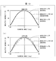
- FIG. 11A is a graph showing the relationship of the light intensity with respect to the emission angle of the light emitting device 500, which is a characteristic when the light emitting device 500 is viewed in the vertical direction.
- FIG. 11B is a graph showing the relationship of the light intensity with respect to the emission angle of the light emitting device 500, which is a characteristic when the light emitting device 500 is viewed in the horizontal direction.
- the directivity characteristics of the green LED chip GY and the directivity characteristics of the red LED chip R are substantially the same, and the directivity characteristics of the blue LED chip B are the same. And the directivity characteristics of the green LED chip GB substantially coincide.
- the directivity characteristics of the red LED chip R and the directivity characteristics of the green LED chip GB substantially coincide with each other, and the green LED chip GY
- the directivity characteristics and the directivity characteristics of the blue LED chip B are almost the same.
- the Zener diode 30 is provided as a protection element in each chip mounting region of the inner lead portion 60.
- Each Zener diode 30 is mounted on the corresponding chip mounting region of the inner lead portion 60 by the conductive paste 31.
- Each Zener diode 30 is connected to the closer one of the inner lead part 62a and the inner lead part 62b by a bonding wire 40.
- Each zener diode 30 is preferably arranged outside the rectangular shape defined by the arrangement of the red LED chip R, the green LED chip GY, the blue LED chip B, and the green LED chip GB. This is to prevent the luminance of light emitted from the light emitting device 500 from being lowered due to the light absorbed by each Zener diode 30.
- FIG. 12 is a top view of the light emitting device according to the present embodiment, and is a view in which illustration of the sealing resin portion is omitted.
- the light emitting device 600 shown in FIG. 12 is different from the light emitting device 100 shown in FIG. 1 in the following points, and is otherwise substantially the same as the light emitting device 100 shown in FIG.
- the light emitting device 600 does not include the common inner lead portion 62 but includes inner lead portions 62a and 62b instead.
- Each of the inner lead parts 62a and 62b functions as a cathode similarly to the common inner lead part 62.
- the red LED chip R, the green LED chip GB, the blue LED chip B, and the green LED chip GY are arranged in the clockwise direction.
- a red LED chip R and a green LED chip GY are connected to the inner lead portion 62a, and a green LED chip GB and a blue LED chip B are connected to the inner lead portion 62b by bonding wires 40, respectively.
- the red LED chip R, the green LED chip GY, the blue LED chip B, and the green LED chip GB are arranged near the center on the main surface side of the substrate 51 so as to be as close as possible to each other.
- the directivity characteristics of the green LED chip GB are matched as much as possible.
- the red LED chip R, the green LED chip GB, the blue LED chip B, and the green LED chip GY are arranged in a rectangular shape. However, in the light emitting device 600, these form a rhombus. It is arranged in.
- FIG. 13A is a graph showing the relationship of the light intensity with respect to the emission angle of the light emitting device 600, which is a characteristic when the light emitting device 600 is viewed in the vertical direction.
- FIG. 13B is a graph showing the relationship of the light intensity with respect to the emission angle of the light emitting device 600, which is a characteristic when the light emitting device 600 is viewed in the horizontal direction.
- the mixed color directivity characteristics of the green LED chip GY and the green LED chip GB, the directivity characteristics of the red LED chip R, and the directivity characteristics of the blue LED chip B are obtained. It almost matches.
- the directivity characteristics of the green LED chip GY and the directivity characteristics of the green LED chip GB substantially coincide. Also, the directivity characteristics of the blue LED chip B and the red LED chip R are not significantly different from the directivity characteristics of the green LED chip GY and the green LED chip GB.
- a case where the second green LED chip is used in combination with a yellow LED chip is also conceivable.
- a case where the dominant wavelength of the second green LED chip is 520 nm or more and 560 nm or less is also conceivable. That is, when a yellow LED chip is used in combination, a general green LED chip that has been conventionally used can also be used as the second green LED chip.
- a light-emitting device is a light-emitting device that emits at least blue-green light and yellow or yellow-green light, and includes a substrate and a plurality of LEDs arranged on the main surface side of the substrate.
- An LED chip group composed of chips, and a sealing portion (sealing resin portion 50) for collectively sealing the LED chip group.
- the LED chip group includes a first green LED chip (green LED chip GB, A green LED chip BT) and a second green LED chip (green LED chip GY), at least one blue LED chip, and at least one red LED chip, The dominant wavelength of one green LED chip is shorter than the dominant wavelength of the second green LED chip.
- the chromaticity range of the blue-green region and the yellow or yellow-green region can be expanded, and the color purity of the blue-green light and the yellow or yellow-green light can be improved.
- the color reproduction range of light emitted from the light emitting device can be greatly expanded.
- the first green LED chip is disposed adjacent to at least one of the at least one blue LED chip, and the second green LED chip is , Disposed adjacent to at least one of the at least one red LED chip.
- green light and blue light can be mixed better, and blue-green light with higher color purity can be realized.
- green light and red light can be mixed more favorably and yellow or yellow-green light with higher color purity can be implement
- the dominant wavelength of the first green LED chip is 480 nm or more and 520 nm or less
- the dominant wavelength of the second green LED chip is 520 nm or more and 560 nm or less.
- the dominant wavelength of the green LED chip having the longest dominant wavelength is 20 nm or more longer than the dominant wavelength of each of the other green LED chips.
- the light-emitting device is the x value of the green LED chip having the longest dominant wavelength on the xy chromaticity coordinates in the CIE chromaticity diagram, and the x value of each of the other green LED chips. The difference is 0.06 or more.
- a light emitting device is a multi-color light emitting device having at least RGB LED chips, and includes a first green LED chip, a green LED chip, a yellow LED chip, a blue LED chip, and a red LED chip. Installed in one package. Moreover, it is preferable that the dominant wavelength of a yellow LED chip shall be 580 nm or more and 610 nm or less. Thereby, since the color purity of blue-green light and yellow light can be improved, a multicolor light-emitting device with favorable color purity can be realized.
- the mixed blue-green hue is improved.
- a light emitting device is a multi-color light emitting device having at least RGB LED chips, and includes a second green LED chip, a green LED chip, a yellow LED chip, a blue LED chip, and a red LED chip. Installed in one package. Moreover, it is preferable that the dominant wavelength of a yellow LED chip shall be 580 nm or more and 610 nm or less. Thereby, since the color purity of yellow-green light and yellow light can be improved, a multicolor light-emitting device with favorable color purity can be realized.
- the mixed yellow-green hue is improved.
- the present invention can be used for a light-emitting device using an LED chip.
Landscapes
- Led Device Packages (AREA)
Abstract
Description
複数のLEDチップ単独で、混色および色純度を良好にし、色の再現範囲を大きく広げることを可能とするマルチカラー発光装置を提供する。
図1は、本実施の形態に係る発光装置の上面図であり、封止樹脂部の図示を省略した図である。
図5は、本実施の形態に係る発光装置の上面図であり、封止樹脂部の図示を省略した図である。なお、説明の便宜上、以下の各実施の形態においては、上記いずれかの実施の形態にて説明した部材と同じ機能を有する部材について、同じ符号を付記し、その説明を省略する。
図6は、本実施の形態に係る通常例の発光装置の上面図であり、封止樹脂部の図示を省略した図である。
表1として、緑色LEDチップGBおよび緑色LEDチップGYの特性を表に示した。なお、表1中、「λd」はドミナント波長、「CIE_x」はCIE色度図におけるxy色度座標上のxの値、「CIE_y」は同座標上のyの値である。

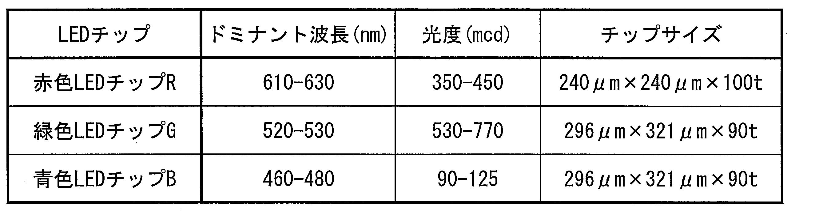
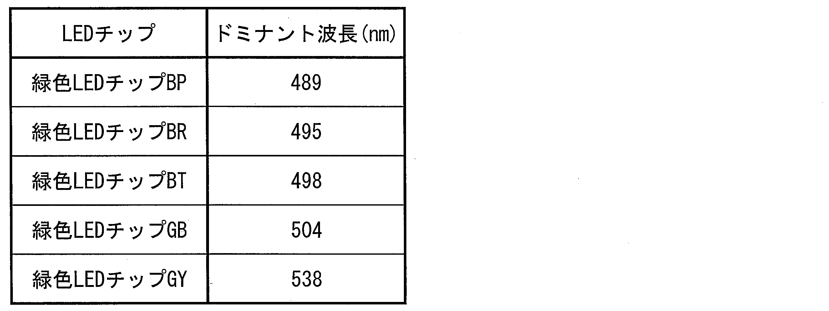
図8は、本実施の形態に係る発光装置の上面図であり、封止樹脂部の図示を省略した図である。
図9は、図1に示す発光装置100の裏面100´の平面図である。なお、説明を分かりやすくするため、本来図9では目視できない、図1に示された基板51の主表面上の各部材を破線で示している。
図10は、本実施の形態に係る発光装置の上面図であり、封止樹脂部の図示を省略した図である。
図12は、本実施の形態に係る発光装置の上面図であり、封止樹脂部の図示を省略した図である。
第2緑色LEDチップを黄色LEDチップと組み合わせて使用する場合も考えられる。この場合、第2緑色LEDチップのドミナント波長が520nm以上560nm以下であるケースも考えられる。すなわち、黄色LEDチップを併用する場合、第2緑色LEDチップとして、従来用いられてきた一般的な緑色LEDチップを用いることもできる。
本発明の一態様に係る発光装置は、少なくとも青緑色の光と黄色または黄緑色の光とを発する発光装置であって、基板と、上記基板の主表面の側に配された、複数のLEDチップからなるLEDチップ群と、上記LEDチップ群を一括封止する封止部(封止樹脂部50)とを備えており、上記LEDチップ群は、第1緑色LEDチップ(緑色LEDチップGB、緑色LEDチップBT)および第2緑色LEDチップ(緑色LEDチップGY)を含む少なくとも2個の緑色LEDチップと、少なくとも1個の青色LEDチップと、少なくとも1個の赤色LEDチップとを含み、上記第1緑色LEDチップのドミナント波長は、上記第2緑色LEDチップのドミナント波長より短い。
51 基板
100 発光装置
200 発光装置
300 発光装置
350 発光装置
400 発光装置
500 発光装置
600 発光装置
B 青色LEDチップ
BT 緑色LEDチップ(第1緑色LEDチップ)
GB 緑色LEDチップ(第1緑色LEDチップ)
GY 緑色LEDチップ(第2緑色LEDチップ)
R 赤色LEDチップ
Claims (5)
- 少なくとも青緑色の光と黄色または黄緑色の光とを発する発光装置であって、
基板と、
上記基板の主表面の側に配された、複数のLEDチップからなるLEDチップ群と、
上記LEDチップ群を一括封止する封止部とを備えており、
上記LEDチップ群は、
第1緑色LEDチップおよび第2緑色LEDチップを含む少なくとも2個の緑色LEDチップと、
少なくとも1個の青色LEDチップと、
少なくとも1個の赤色LEDチップとを含み、
上記第1緑色LEDチップのドミナント波長は、上記第2緑色LEDチップのドミナント波長より短いことを特徴とする発光装置。 - 上記第1緑色LEDチップが、上記少なくとも1個の青色LEDチップのうちの少なくとも1個に隣接して配されており、
上記第2緑色LEDチップが、上記少なくとも1個の赤色LEDチップのうちの少なくとも1個に隣接して配されていることを特徴とする請求項1に記載の発光装置。 - 上記第1緑色LEDチップのドミナント波長が、480nm以上520nm以下であり、
上記第2緑色LEDチップのドミナント波長が、520nm以上560nm以下であることを特徴とする請求項1または2に記載の発光装置。 - 最もドミナント波長が長い緑色LEDチップのドミナント波長は、他の各緑色LEDチップのドミナント波長より20nm以上長いことを特徴とする請求項1から3のいずれか1項に記載の発光装置。
- CIE色度図におけるxy色度座標上において、
最もドミナント波長が長い緑色LEDチップのxの値と、他の各緑色LEDチップのxの値との差が0.06以上であることを特徴とする請求項1から4のいずれか1項に記載の発光装置。
Priority Applications (3)
| Application Number | Priority Date | Filing Date | Title |
|---|---|---|---|
| US15/307,597 US9818731B2 (en) | 2014-05-30 | 2015-04-14 | Light emitting device |
| CN201580010216.9A CN106463583B (zh) | 2014-05-30 | 2015-04-14 | 发光装置 |
| JP2016523374A JP6130064B2 (ja) | 2014-05-30 | 2015-04-14 | 発光装置 |
Applications Claiming Priority (2)
| Application Number | Priority Date | Filing Date | Title |
|---|---|---|---|
| JP2014113457 | 2014-05-30 | ||
| JP2014-113457 | 2014-05-30 |
Publications (1)
| Publication Number | Publication Date |
|---|---|
| WO2015182272A1 true WO2015182272A1 (ja) | 2015-12-03 |
Family
ID=54698613
Family Applications (1)
| Application Number | Title | Priority Date | Filing Date |
|---|---|---|---|
| PCT/JP2015/061454 Ceased WO2015182272A1 (ja) | 2014-05-30 | 2015-04-14 | 発光装置 |
Country Status (4)
| Country | Link |
|---|---|
| US (1) | US9818731B2 (ja) |
| JP (1) | JP6130064B2 (ja) |
| CN (1) | CN106463583B (ja) |
| WO (1) | WO2015182272A1 (ja) |
Cited By (3)
| Publication number | Priority date | Publication date | Assignee | Title |
|---|---|---|---|---|
| JP2017130497A (ja) * | 2016-01-18 | 2017-07-27 | 日亜化学工業株式会社 | 発光装置および発光装置を備えたバックライト |
| JP2017175057A (ja) * | 2016-03-25 | 2017-09-28 | 東芝ライテック株式会社 | 発光装置、および照明装置 |
| US10944036B2 (en) | 2019-03-18 | 2021-03-09 | Rohm Co., Ltd. | Semiconductor light-emitting device |
Families Citing this family (1)
| Publication number | Priority date | Publication date | Assignee | Title |
|---|---|---|---|---|
| JP6606946B2 (ja) * | 2015-09-21 | 2019-11-20 | 豊田合成株式会社 | 発光素子 |
Citations (5)
| Publication number | Priority date | Publication date | Assignee | Title |
|---|---|---|---|---|
| JPH07175423A (ja) * | 1993-10-29 | 1995-07-14 | Toyoda Gosei Co Ltd | 表示装置 |
| JPH10136159A (ja) * | 1996-10-31 | 1998-05-22 | Citizen Electron Co Ltd | カラーイメージスキャナ用光源 |
| JP2005321727A (ja) * | 2004-05-11 | 2005-11-17 | Sony Corp | バックライト装置及びカラー液晶表示装置 |
| JP2008269947A (ja) * | 2007-04-20 | 2008-11-06 | Hitachi Displays Ltd | 液晶表示装置 |
| JP2011192738A (ja) * | 2010-03-12 | 2011-09-29 | Seiwa Electric Mfg Co Ltd | 発光装置 |
Family Cites Families (7)
| Publication number | Priority date | Publication date | Assignee | Title |
|---|---|---|---|---|
| JP3124208B2 (ja) | 1995-03-30 | 2001-01-15 | 株式会社東芝 | Led表示器及びled表示システム |
| JPH10161567A (ja) | 1996-12-05 | 1998-06-19 | Matsushita Electron Corp | 発光単位ブロック及び発光ダイオード表示装置 |
| JP2001177156A (ja) | 1999-12-14 | 2001-06-29 | Koha Co Ltd | 側面発光型ledランプ |
| JP2002082635A (ja) | 2000-09-07 | 2002-03-22 | Sharp Corp | カラーledディスプレイ装置 |
| JP4263905B2 (ja) | 2002-12-11 | 2009-05-13 | パナソニック株式会社 | Led光源、led照明装置、およびled表示装置 |
| DE102010012423A1 (de) * | 2009-12-21 | 2011-06-22 | OSRAM Opto Semiconductors GmbH, 93055 | Lumineszenzdiodenanordnung, Hinterleuchtungsvorrichtung und Anzeigevorrichtung |
| JP5799212B2 (ja) | 2010-09-21 | 2015-10-21 | パナソニックIpマネジメント株式会社 | 発光モジュール、バックライト装置および表示装置 |
-
2015
- 2015-04-14 CN CN201580010216.9A patent/CN106463583B/zh not_active Expired - Fee Related
- 2015-04-14 US US15/307,597 patent/US9818731B2/en not_active Expired - Fee Related
- 2015-04-14 JP JP2016523374A patent/JP6130064B2/ja not_active Expired - Fee Related
- 2015-04-14 WO PCT/JP2015/061454 patent/WO2015182272A1/ja not_active Ceased
Patent Citations (5)
| Publication number | Priority date | Publication date | Assignee | Title |
|---|---|---|---|---|
| JPH07175423A (ja) * | 1993-10-29 | 1995-07-14 | Toyoda Gosei Co Ltd | 表示装置 |
| JPH10136159A (ja) * | 1996-10-31 | 1998-05-22 | Citizen Electron Co Ltd | カラーイメージスキャナ用光源 |
| JP2005321727A (ja) * | 2004-05-11 | 2005-11-17 | Sony Corp | バックライト装置及びカラー液晶表示装置 |
| JP2008269947A (ja) * | 2007-04-20 | 2008-11-06 | Hitachi Displays Ltd | 液晶表示装置 |
| JP2011192738A (ja) * | 2010-03-12 | 2011-09-29 | Seiwa Electric Mfg Co Ltd | 発光装置 |
Cited By (6)
| Publication number | Priority date | Publication date | Assignee | Title |
|---|---|---|---|---|
| JP2017130497A (ja) * | 2016-01-18 | 2017-07-27 | 日亜化学工業株式会社 | 発光装置および発光装置を備えたバックライト |
| US10274667B2 (en) | 2016-01-18 | 2019-04-30 | Nichia Corporation | Light-emitting device with two green light-emitting elements with different peak wavelengths and backlight including light-emitting device |
| JP2017175057A (ja) * | 2016-03-25 | 2017-09-28 | 東芝ライテック株式会社 | 発光装置、および照明装置 |
| US10944036B2 (en) | 2019-03-18 | 2021-03-09 | Rohm Co., Ltd. | Semiconductor light-emitting device |
| US11532776B2 (en) | 2019-03-18 | 2022-12-20 | Rohm Co., Ltd. | Semiconductor light-emitting device |
| US12087896B2 (en) | 2019-03-18 | 2024-09-10 | Rohm Co., Ltd. | Semiconductor light-emitting device |
Also Published As
| Publication number | Publication date |
|---|---|
| JPWO2015182272A1 (ja) | 2017-04-20 |
| CN106463583A (zh) | 2017-02-22 |
| US20170047311A1 (en) | 2017-02-16 |
| JP6130064B2 (ja) | 2017-05-24 |
| US9818731B2 (en) | 2017-11-14 |
| CN106463583B (zh) | 2019-03-08 |
Similar Documents
| Publication | Publication Date | Title |
|---|---|---|
| US8598608B2 (en) | Light emitting device | |
| US10153408B2 (en) | Light-emitting apparatus and illumination apparatus | |
| US10508778B2 (en) | Light-emitting device | |
| CN102110682A (zh) | 发光装置及其制造方法 | |
| US11756939B2 (en) | Light emitting element with particular phosphors | |
| JP6130064B2 (ja) | 発光装置 | |
| JP6230392B2 (ja) | 発光装置 | |
| JP2008288412A (ja) | Led発光装置 | |
| JP2000349345A (ja) | 半導体発光装置 | |
| JP2016119381A (ja) | Led発光モジュール | |
| JP2018056474A (ja) | 発光装置及び発光装置の製造方法 | |
| TWI468810B (zh) | 背光模組 | |
| CN119937198A (zh) | 背光光源及显示设备 | |
| JP2018182309A (ja) | 発光装置 | |
| JP6807686B2 (ja) | 発光装置 | |
| US9406858B2 (en) | LED module | |
| JP2015233048A (ja) | 発光装置 | |
| CN103700655A (zh) | 一种贴片led | |
| CN103618040A (zh) | 一种白光二极管 | |
| JP2013135082A (ja) | 発光装置 | |
| JP6681581B2 (ja) | 発光装置、及び、照明装置 | |
| JP2018093151A (ja) | 発光装置 | |
| JP2021019078A (ja) | 発光装置 | |
| JP2018156966A (ja) | 発光装置及び照明装置 | |
| CN215988825U (zh) | 多色led集成光源 |
Legal Events
| Date | Code | Title | Description |
|---|---|---|---|
| 121 | Ep: the epo has been informed by wipo that ep was designated in this application |
Ref document number: 15799521 Country of ref document: EP Kind code of ref document: A1 |
|
| DPE2 | Request for preliminary examination filed before expiration of 19th month from priority date (pct application filed from 20040101) | ||
| ENP | Entry into the national phase |
Ref document number: 2016523374 Country of ref document: JP Kind code of ref document: A |
|
| WWE | Wipo information: entry into national phase |
Ref document number: 15307597 Country of ref document: US |
|
| NENP | Non-entry into the national phase |
Ref country code: DE |
|
| 122 | Ep: pct application non-entry in european phase |
Ref document number: 15799521 Country of ref document: EP Kind code of ref document: A1 |