WO2015181981A1 - 電子顕微鏡による分析方法及び電子顕微鏡 - Google Patents
電子顕微鏡による分析方法及び電子顕微鏡 Download PDFInfo
- Publication number
- WO2015181981A1 WO2015181981A1 PCT/JP2014/064530 JP2014064530W WO2015181981A1 WO 2015181981 A1 WO2015181981 A1 WO 2015181981A1 JP 2014064530 W JP2014064530 W JP 2014064530W WO 2015181981 A1 WO2015181981 A1 WO 2015181981A1
- Authority
- WO
- WIPO (PCT)
- Prior art keywords
- electron microscope
- image
- microscope image
- electron
- electron beam
- Prior art date
- Legal status (The legal status is an assumption and is not a legal conclusion. Google has not performed a legal analysis and makes no representation as to the accuracy of the status listed.)
- Ceased
Links
Images








Classifications
-
- H—ELECTRICITY
- H01—ELECTRIC ELEMENTS
- H01J—ELECTRIC DISCHARGE TUBES OR DISCHARGE LAMPS
- H01J37/00—Discharge tubes with provision for introducing objects or material to be exposed to the discharge, e.g. for the purpose of examination or processing thereof
- H01J37/02—Details
- H01J37/22—Optical, image processing or photographic arrangements associated with the tube
- H01J37/222—Image processing arrangements associated with the tube
-
- H—ELECTRICITY
- H01—ELECTRIC ELEMENTS
- H01J—ELECTRIC DISCHARGE TUBES OR DISCHARGE LAMPS
- H01J37/00—Discharge tubes with provision for introducing objects or material to be exposed to the discharge, e.g. for the purpose of examination or processing thereof
- H01J37/02—Details
- H01J37/21—Means for adjusting the focus
-
- H—ELECTRICITY
- H01—ELECTRIC ELEMENTS
- H01J—ELECTRIC DISCHARGE TUBES OR DISCHARGE LAMPS
- H01J37/00—Discharge tubes with provision for introducing objects or material to be exposed to the discharge, e.g. for the purpose of examination or processing thereof
- H01J37/02—Details
- H01J37/22—Optical, image processing or photographic arrangements associated with the tube
-
- H—ELECTRICITY
- H01—ELECTRIC ELEMENTS
- H01J—ELECTRIC DISCHARGE TUBES OR DISCHARGE LAMPS
- H01J37/00—Discharge tubes with provision for introducing objects or material to be exposed to the discharge, e.g. for the purpose of examination or processing thereof
- H01J37/02—Details
- H01J37/244—Detectors; Associated components or circuits therefor
-
- H—ELECTRICITY
- H01—ELECTRIC ELEMENTS
- H01J—ELECTRIC DISCHARGE TUBES OR DISCHARGE LAMPS
- H01J37/00—Discharge tubes with provision for introducing objects or material to be exposed to the discharge, e.g. for the purpose of examination or processing thereof
- H01J37/26—Electron or ion microscopes; Electron or ion diffraction tubes
- H01J37/261—Details
- H01J37/265—Controlling the tube; circuit arrangements adapted to a particular application not otherwise provided, e.g. bright-field-dark-field illumination
-
- H—ELECTRICITY
- H01—ELECTRIC ELEMENTS
- H01J—ELECTRIC DISCHARGE TUBES OR DISCHARGE LAMPS
- H01J37/00—Discharge tubes with provision for introducing objects or material to be exposed to the discharge, e.g. for the purpose of examination or processing thereof
- H01J37/26—Electron or ion microscopes; Electron or ion diffraction tubes
- H01J37/28—Electron or ion microscopes; Electron or ion diffraction tubes with scanning beams
-
- H—ELECTRICITY
- H01—ELECTRIC ELEMENTS
- H01J—ELECTRIC DISCHARGE TUBES OR DISCHARGE LAMPS
- H01J2237/00—Discharge tubes exposing object to beam, e.g. for analysis treatment, etching, imaging
- H01J2237/153—Correcting image defects, e.g. stigmators
- H01J2237/1534—Aberrations
-
- H—ELECTRICITY
- H01—ELECTRIC ELEMENTS
- H01J—ELECTRIC DISCHARGE TUBES OR DISCHARGE LAMPS
- H01J2237/00—Discharge tubes exposing object to beam, e.g. for analysis treatment, etching, imaging
- H01J2237/22—Treatment of data
- H01J2237/221—Image processing
- H01J2237/223—Fourier techniques
-
- H—ELECTRICITY
- H01—ELECTRIC ELEMENTS
- H01J—ELECTRIC DISCHARGE TUBES OR DISCHARGE LAMPS
- H01J2237/00—Discharge tubes exposing object to beam, e.g. for analysis treatment, etching, imaging
- H01J2237/22—Treatment of data
- H01J2237/226—Image reconstruction
- H01J2237/228—Charged particle holography
-
- H—ELECTRICITY
- H01—ELECTRIC ELEMENTS
- H01J—ELECTRIC DISCHARGE TUBES OR DISCHARGE LAMPS
- H01J2237/00—Discharge tubes exposing object to beam, e.g. for analysis treatment, etching, imaging
- H01J2237/26—Electron or ion microscopes
- H01J2237/28—Scanning microscopes
- H01J2237/2802—Transmission microscopes
Definitions
- the present invention relates to an analysis method using an electron microscope and an electron microscope.
- the sample moves at the atomic level while changing the focal position in this way, it is difficult to detect an atomic shift or strain between the substrate and the film.
- the film formed on the substrate is thin, when the image of the film is acquired, information on the substrate is also included, so the atomic deviation and distortion of the film formed on the substrate are clearly identified. It was difficult to detect.
- the electron beam emitted from the electron source is accelerated and irradiated so that the focal point of the electron beam is positioned on the sample, and the sample is transmitted or scattered by the sample.
- a first electron microscope image detector that detects an annular dark field image in the sample by detecting an electron beam; and a second electron microscope image detector that detects a medium-angle region bright field image in the sample.
- the sample has a film formed on the surface of the substrate, and the substrate includes fluorine or an element lighter than fluorine, and the film of the sample has the electron beam on the film.
- the substrate in the sample is irradiated with an electron beam so that the focal point of the electron beam is positioned, and then the third electron microscope image and the second electron microscope image detector are detected by the first electron microscope image detector.
- the second electron microscope image and the fourth electron microscope image are aligned.
- the scanning transmission electron microscope in the present embodiment is a confocal scanning transmission electron microscope apparatus, and includes a field emission electron gun 11 serving as an electron source that emits an electron beam 10, and an acceleration unit that accelerates the emitted electron beam 10. 12 is provided.
- the electron beam 10 accelerated in the accelerating unit 12 is converged by converging lenses 13 and 14 (in the drawing, the converging lens shows a two-stage structure), and then irradiated on the sample 40 by the converging lens diaphragm 15.
- the irradiation half angle of the electron beam is adjusted.
- the electron beam probe composed of the electron beam 10 thus converged is deflected by the scanning coil 16 serving as an electron beam scanning unit, and after passing through the spherical aberration correction unit 17, becomes an extremely minute electron beam probe by the objective lens 18.
- the sample 40 is irradiated.
- the electron beam 10 can be scanned by deflecting the electron beam 10 by the scanning coil 16, and an atomic image or the like constituting the sample 40 can be obtained.
- the spherical aberration correction unit 17 uses the spherical aberration correction device described above, and can perform spherical aberration correction and chromatic aberration correction of the electron beam 10, and the spherical aberration correction unit 17 sets the spherical aberration coefficient to 1 ⁇ m or less. Can be.
- the two-stage converging lenses 13 and 14 are shown.
- the converging lenses may have a structure in which a plurality of stages are arranged.
- the electron beam that has become an extremely minute electron beam probe whose focal position has been adjusted is applied to the sample 40 and transmitted through the sample 40 or scattered by the sample 40.
- the electron beam transmitted through the sample 40 or scattered and scattered in the sample 40 in this way is passed through the projection lens 19 and the first electron microscope image detector 21 and the second electron installed at the rear stage of the sample 40. It is detected by the microscope image detector 22.
- the first electron microscope image detector 21 is for detecting an ADF (annular dark-filed) -STEM image, and is formed in a ring shape with an opening 21a formed at the center. ing.
- the second electron microscope image detector 22 is for detecting a MABF (middle-angle bright-field) -STEM image, and an opening of the first electron microscope image detector 21.
- the electron beam that has passed through 21a is detected.
- FIG. 2 is a diagram showing the relationship between the electron beam 10 irradiated on the sample 40 and the first electron microscope image detector 21 and the second electron microscope image detector 22.
- the scanning transmission electron microscope in the present embodiment has a control analysis unit 50.
- the control analysis unit 50 includes an image displacement amount calculation unit 51, an image registration unit 52, an image normalization unit 53, an image calculation unit 54, and an image output unit 55, and the image output from the image output unit 55.
- the information is displayed on the display unit 60 connected to the control analysis unit 50.
- the control analysis unit 50 controls the converging lenses 13 and 14, the spherical aberration correction unit 17, the objective lens 18, the projection lens 19, and the like, and the first electron microscope image detector 21 and the second electron microscope image. Analysis or the like is performed based on information detected by the detector 22.
- a sample 40 to be analyzed is formed by growing a material different from the substrate 41 on a substrate 41 made of a crystal substrate such as an oxide as shown in FIG. As a result, the film 42 is formed.
- the substrate 41 is made of a material containing an element lighter than fluorine, and is made of, for example, a crystal such as an oxide, nitride, fluoride, or carbide.
- an ADF-STEM image is acquired simultaneously by the first electron microscope image detector 21 and a MABF-STEM image is acquired simultaneously by the second electron microscope image detector 22.
- ADF-STEM is an observation method in which strong intensity appears at positions where heavy elements are present
- MABF-STEM is an observation method in which strong intensity appears at positions where light elements are present.
- the information on the atomic position is obtained by irradiating the electron beam perpendicularly to the substrate surface of the sample 40, and therefore, the substrate 41 and the substrate 41 in the electron beam incident direction A membrane 42 is present.
- the focal position of the electron beam is the film 42
- information on the heavy elements contained in the material forming the film 42 and the heavy elements contained in the material forming the substrate 41 are used. May appear at the same time. That is, when the focal position of the electron beam is the film 42, not only information on the heavy elements contained in the material forming the film 42 but also information on the heavy elements contained in the material forming the substrate 41. May also appear at the same time. In this case, it is not possible to obtain only information on the film 42. This becomes more prominent when the film 42 is thin.
- image position deviation correction is performed based on the MABF-STEM image when the focal position is the substrate 41 and the MABF-STEM image when the focal position is the film 42.
- accurate alignment can be performed between the ADF-STEM image when the focal position is the substrate 41 and the ADF-STEM image when the focal position is the film 42.
- the information on the heavy elements contained in the material forming the film 42 and the heavy elements contained in the material forming the substrate 41 are shown. Information may appear at the same time.
- the ADF-STEM image when the focal position of the electron beam is the substrate 41 only information on heavy elements contained in the material forming the substrate 41 appears. Therefore, in the present embodiment, based on the MABF-STEM image when the focal position is the film 42 and when the focal position is the substrate 41, the ADF-STEM image when the focal position is the film 42 and the electron beam Alignment with the ADF-STEM image when the focal position is the substrate 41 is performed.
- image calculation is performed to subtract the ADF-STEM image when the electron beam focal position is the film 42 from the ADF-STEM image when the electron beam focal position is the substrate 41. Thereby, information on the position of the heavy element contained in the material forming the film 42 can be obtained as an image.
- the MABF-STEM image and the ADF-STEM image when the electron beam focal position is the film 42 first, the MABF-STEM image and the ADF-STEM image when the electron beam focal position is the film 42, and the MABF-STEM image and the ADF when the electron beam focal position is the substrate 41.
- image information on the film 42 is obtained by performing image operations on the ADF-STEM image when the focal position of the electron beam is the film 42 and the ADF-STEM image when the focal position of the electron beam is the substrate 41. It is an analysis method to acquire.
- an electron beam converged to nanometer or less is incident on the sample 40, diffracted in the sample 40, and reaches an annular ADF detector (annular dark filed detector) installed on the diffraction image plane.
- the counted number of electrons is synchronized with the position of the incident electrons to obtain the image intensity.
- This image is generally called a high-angle annular dark-field (HAADF) -STEM image, and is a kind of ADF-STEM image.
- HAADF high-angle annular dark-field
- a characteristic of the HAADF-SETM image is that an intensity corresponding to the atomic number of an element in the atom can be obtained at the position of the atom.
- the contrast of the image is extremely insensitive to the focal point of the electromagnetic lens that converges the electron beam and the thickness of the sample, it is possible to obtain an image excellent in atomic direct visibility.
- the spatial resolution of the image depends on the converged diameter of the converged electron beam, and when the spherical aberration correction apparatus is used, the spatial resolution is 1 ⁇ m or less. can do.
- an annular first electron microscope image detector 21 when detecting the HAADF-STEM image, an annular first electron microscope image detector 21 is used. Therefore, the electron beam that has passed through the opening 21a formed in the central portion of the first electron microscope image detector 21 is detected by the disc-shaped second electron microscope image detector 22.
- An image obtained by the electron beam detected by the disc-shaped second electron microscope image detector 22 is called a bright-field (BF) -STEM image.
- the characteristics of the BF-STEM image vary greatly depending on the setting of the capturing condition of the disk-shaped second electron microscope image detector 22.
- An image obtained by increasing the capture angle is known as a complementary image of the HAADF-STEM image, and is classified as a high-angle bright-field (HABF) -STEM image.
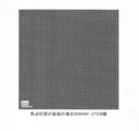
- a BF-STEM image acquired at a medium capture angle (9 m radians to 12 m radians) is classified as a MABF-STEM image, and a bright image is obtained at the position of a light element.
- a sample 40 a SrTiO 3 crystal substrate is used as the substrate 41, and a film 42 is formed on the substrate 41, which is the crystal substrate, to be a crystal film obtained by crystal growth growth of LaCoO 3 .
- a structural model was used.
- the thickness of the substrate 41 is 68 nm
- the thickness of the film 42 is 12 nm
- the atomic positions in the substrate 41 and the film 42 are based on the unit cell (1/4 1/4 0).
- the incident direction of the electron beam is the [0 0 1] direction
- the method for acquiring a three-dimensional tomographic image is the same as the method disclosed in Patent Document 1.
- the electron beam formed by the spherical aberration-corrected electromagnetic lens has an extremely shallow depth of focus, and the electromagnetic beam is positioned so that the focal point is located at the portion to be observed. An image is obtained by changing the focal point of the lens.
- FIG. 5 when the focal position of the electron beam is the film 42, the calculation was performed in a defocused state so that the focal point is located 5 nm deeper in the depth direction than the surface.
- the focal position of the electron beam is the substrate 41, the calculation was performed in a defocused state so that the focal point is located 30 nm deeper than the surface.
- 6A and 6B show the case where the focal position of the electron beam is the film 42.
- FIG. 6C and 6D are for the case where the focal position of the electron beam is the substrate 41.
- FIG. 6C is a MABF-STEM image when a position 30 nm deep in the depth direction from the surface of the sample 40 on the film 42 side is used as the focal position of the electron beam
- FIG. I is an ADF-STEM image in this case.
- the MABF-STEM image shown in FIG. 6 (a) is described as a first electron microscope image
- the ADF-STEM image shown in FIG. 6 (b) is referred to as a second electron microscope image. May be described.
- the MABF-STEM image shown in FIG. 6C may be described as a third electron microscope image
- the ADF-STEM image shown in FIG. 6D may be described as a fourth electron microscope image. .
- FIG. 7A shows a state where the focal position of the electron beam is the film 42, that is, a case where the position deeper than the surface of the sample 40 by 5 nm in the depth direction is the focal position of the electron beam.
- FIG. 7B is a MABF-STEM image (first electron microscope image) obtained in this case
- FIG. 7C is an ADF-STEM image (second electron microscope image).
- the position of the light element in the substrate 41 that is, the position of oxygen (O) in SrTiO 3 forming the substrate 41 is the most. Illustrated brightly.
- the positions of the heavy elements in the substrate 41 and the heavy elements in the film 42 are shown brightly. That is, the positions of Sr and Ti in SrTiO 3 forming the substrate 41 and the positions of La and Co in LaCoO 3 forming the film 42 are shown brightly.
- the ADF-STEM image (second electron microscope image) shown in FIG. 7 (c) heat scattered scattered electrons scattered from heavy elements existing at the focal position of the electron beam are detected. Heavy elements at the focal point appear mainly in the image.
- the MABF-STEM image (first electron microscope image) shown in FIG. 7B the position where the light elements are the largest in the entire sample 40 becomes bright.
- FIG. 8A shows a state where the focal position of the electron beam is the substrate, that is, a position where the position deeper than the surface of the sample 40 by 30 nm in the depth direction is the focal position of the electron beam.
- FIG. 8B is a MABF-STEM image (third electron microscope image) obtained in this case
- FIG. 8C is an ADF-STEM image (fourth electron microscope image).
- the position of the light element in the substrate 41 that is, the position of oxygen (O) in SrTiO 3 forming the substrate 41 is the most. Illustrated brightly.
- the heavy elements in the substrate 41 that is, the positions of Sr and Ti in SrTiO 3 forming the substrate 41 are shown brightly. Has been.
- a MABF-STEM image first electron microscope image
- a MABF-STEM image when the focal position of the electron beam is the film 42 and a MABF-STEM image when the focal position of the electron beam is the substrate 41
- the amount of image displacement is calculated from the third electron microscope image.
- an ADF-STEM image second electron microscope image
- an ADF-STEM image fourth electron microscope image
- an ADF-STEM image fourth electron microscope image
- an ADF-STEM image (second electron microscope image) when the focal position of the electron beam is the film 42 and an ADF-STEM image (fourth electron microscope image) when the focal position of the electron beam is the substrate 41.
- the brightness of the image is normalized.
- the focal position of the electron beam shown in FIG. 9A is the film 42
- Image calculation for drawing an ADF-STEM image (fourth electron microscope image) in the case of the substrate 41 is performed.
- an image showing the structure of the film 42 that is, the positions of La and Co, which are heavy elements in LaCoO 3 forming the film 42, can be obtained as shown in FIG. 9C. .
- a correlation method or a phase A correlation limiting method or the like can be used as a method of calculating the image positional deviation amount using the MABF-STEM image when the electron beam focal position is the film 42 and the MABF-STEM image when the electron beam focal position is the substrate 41.
- step 102 an ADF-STEM image (first electron microscope image) and a MABF-STEM image (second electron microscope image) when the focal position of the electron beam is the film 42 are acquired.
- the electron beam is adjusted so that the focal position of the electron beam is positioned on the film 42 of the sample 40 and irradiated with the electron beam, and the electron beam transmitted through the sample 40 or scattered in the sample 40 is converted into the first electron.
- Detection is performed by the microscope image detector 21 and the second electron microscope image detector 22.
- the first electron microscope image detector 21 detects an ADF-STEM image (first electron microscope image) when the focal position of the electron beam is the film 42.
- the second electron microscope image detector 22 detects a MABF-STEM image (second electron microscope image) when the focal position of the electron beam is the film 42.
- step 104 an ADF-STEM image (third electron microscope image) and a MABF-STEM image (fourth electron microscope image) when the focal position of the electron beam is the substrate 41 are acquired.
- the electron beam is adjusted so that the focal position of the electron beam is positioned on the substrate 41 of the sample 40 and irradiated with the electron beam, and the electron beam transmitted through the sample 40 or scattered in the sample 40 is converted into the first electron.
- Detection is performed by the microscope image detector 21 and the second electron microscope image detector 22.
- the first electron microscope image detector 21 detects an ADF-STEM image (third electron microscope image) when the focal position of the electron beam is the substrate 41.
- the second electron microscope image detector 22 detects a MABF-STEM image (fourth electron microscope image) when the focal position of the electron beam is the substrate 41.
- step 106 an image position deviation amount is calculated when the focal position of the electron beam is the film 42 and when the focal position of the electron beam is the substrate 41.
- the image position deviation amount calculation unit 51 in the control analysis unit 50 includes the MABF-STEM image (first electron microscope image) and the electron beam focus position when the electron beam focus position is the film 42. 41 is input as a MABF-STEM image (third electron microscope image). Thereafter, in the image position deviation amount calculation unit 51, the MABF-STEM image (first electron microscopic image) when the focal position of the electron beam is the film 42 and the MABF-STEM when the focal position of the electron beam is the substrate 41. An image position shift amount is calculated based on the image (third electron microscope image).
- step 108 an ADF-STEM image (second electron microscope image) in the case where the focal position of the electron beam is the film 42 and an ADF-STEM image in the case where the focal position of the electron beam is the substrate 41.
- Alignment with (fourth electron microscope image) is performed. That is, based on the image position shift amount calculated in step 106, the focal position of the electron beam is the position of the substrate 41 with respect to the ADF-STEM image (second electron microscope image) when the focal position of the electron beam is the film 42.
- the ADF-STEM image (fourth electron microscope image) in the case is moved. This step is performed in the image alignment unit 52.
- an ADF-STEM image when the electron beam focal position is the film 42 and an ADF-STEM image (fourth electron microscope image) when the electron beam focal position is the substrate 41.
- the position of the ADF-STEM image when the focal position of the electron beam is the film 42
- the ADF-STEM image fourth image
- the position of the electron microscope image can be matched.
- step 110 an ADF-STEM image (second electron microscope image) when the focal position of the electron beam is the film 42 and an ADF-STEM image when the focal position of the electron beam is the substrate 41 (Normization of brightness intensity with the fourth electron microscope image) is performed.
- This normalization is performed in the image normalization unit 53.
- an ADF-STEM image second electron microscope image
- an ADF-STEM image fourth electron
- the brightness of the heavy elements on the substrate 41 is substantially matched.
- step 112 an ADF-STEM image when the focal position of the electron beam is the substrate 41 (second electron microscope image) when the focal position of the electron beam is the film 42 (second electron microscope image) Image calculation for drawing a fourth electron microscope image) is performed.
- an image on the film 42 is obtained.
- the image calculation unit 54 the ADF-STEM image in the case where the focal position of the electron beam is the substrate 41 from the ADF-STEM image (second electron microscope image) when the focal position of the electron beam is the film 42.
- Image calculation for drawing (fourth electron microscope image) is performed.
- An image on the film 42 obtained by this image calculation is displayed on the display unit 60 via the image output unit 55.
- film 42 when formed by LaCoO 3, the structure of LaCoO 3 forming the film 42, i.e., it is possible to know the position of La and Co in LaCoO 3.
- FIG. 11 is an ADF-STEM image (second electron microscopic image) when the focal position of the electron beam is the film 42
- FIG. 11 is an ADF-STEM image when the focal position of the electron beam is the substrate 41 ( 4th electron microscope image).
- a MABF-STEM image first electron microscopic image
- a MABF-STEM image third electron beam focus position when the electron beam focal position is the substrate 41
- the image positional deviation amount in the mutual image is calculated.
- an ADF-STEM image (second electron microscope image) when the focal position of the electron beam is the film 42 and an ADF-STEM image (fourth electron microscope image) when the focal position of the electron beam is the substrate 41. Align with the.
- an ADF-STEM image (second electron microscope image) when the focal position of the electron beam is the film 42 and an ADF-STEM image (fourth electron microscope image) when the focal position of the electron beam is the substrate 41.
- normalization is performed to make the brightness of the image uniform.
- an ADF-STEM image (fourth electron microscope image) in the case where the focal position of the electron beam is the substrate 41 is obtained from an ADF-STEM image (second electron microscope image) in the case where the focal position of the electron beam is the film 42.
- Perform image calculation to subtract thereby, as shown in FIG. 13, an image of the LaCoO 3 growth film, which is the film 42 formed on the substrate 41, can be obtained.
- FIG. 14 shows an image obtained by performing FFT (Fast Fourier Transform) on the image shown in FIG. 13 thus obtained.
- an image of the atomic arrangement in the film 42 formed on the substrate 41 can be obtained, and distortion and the like in the film 42 formed on the substrate 41 can be easily performed. It becomes possible to know.
Landscapes
- Chemical & Material Sciences (AREA)
- Analytical Chemistry (AREA)
- Engineering & Computer Science (AREA)
- Computer Vision & Pattern Recognition (AREA)
- Analysing Materials By The Use Of Radiation (AREA)
Abstract
基板に成膜されている膜の原子的なずれや歪みを明確に検出する。 環状暗視野像(ADF-STEM像)を検出する第1の検出器と、中角度領域明視野像(MABF-STEM像)を検出する第2の検出器とを有する電子顕微鏡による分析方法において、試料はフッ素又はフッ素よりも軽い元素を含む基板の表面に膜が形成されたものであり、焦点位置が前記膜の場合の環状暗視野像及び中角度領域明視野像を取得し、焦点位置が前記基板の場合の環状暗視野像及び中角度領域明視野像を取得し、前記2枚の中角度領域明視野像に基づき前記2枚の環状暗視野像の位置合わせを行い、前記2枚の環状暗視野像の差分像を取得する。
Description
本発明は、電子顕微鏡による分析方法及び電子顕微鏡に関するものである。
透過型電子顕微鏡(Transmission Electron Microscope:TEM)や走査透過電子顕微鏡(Scanning Transmission Electron Microscope:STEM)は、材料の原子レベルでの構造解析や組成解析を行う上で、極めて重要な技法の一つである。しかしながら、透過型電子顕微鏡等においては、試料を透過した電子線を用いて画像を取得するため、得られた画像における構造は、2次元的な対称性を反映したものとなる。そのため、古くから透過型電子顕微鏡等を用いた3次元断層像の取得方法を開発することは、大きな研究課題の一つとされている。近年、球面収差補正装置の実現により、浅い焦点深度の電磁レンズを形成することが可能となり、この球面収差補正装置を用いて、焦点位置を変化させて像を取得することにより、3次元断層像を取得することが可能となった。このような球面収差補正装置を用いた実際の観察例として、基板の表面に成長させた膜や境界をピンポイントで観察した結果が開示されている(例えば、特許文献1、非特許文献1)。
Nature Materials, 8 (2009) 654.
ところで、透過型電子顕微鏡等により前述の3次元断層像を取得する際には、各々の深さ位置において取得される像の正確な位置関係や原子的なずれや歪みが明確であることが求められている。例えば、基板上に基板とは異なる組成の材料の膜を成長させたような試料においては、基板と膜との間における原子レベルでの関係性や膜の原子的なずれや歪みを明確に知ることが重要である。しかしながら、特許文献1に記載されている方法では、焦点位置を変化させることにより、基板と膜とにおける画像の各々を取得する方法であるため、焦点位置を変化させている間に、試料が原子レベルで動いてしまう(ドリフト)。このように焦点位置を変化させている間に、試料が原子レベルで動いてしまうと、基板と膜との間における原子的なずれや歪を検出することは困難である。また、基板に成膜されている膜は薄いため、膜の画像を取得した場合、基板の情報も含まれてしまうため、基板に成膜されている膜の原子的なずれや歪みを明確に検出することは困難であった。
よって、基板に成膜されている膜の原子的なずれや歪みを明確に検出することのできる電子顕微鏡による分析方法が求められている。
本実施の形態の一観点によれば、電子源より放出された電子線を加速し、試料に前記電子線の焦点が位置するように照射して、前記試料を透過または前記試料により散乱された電子線を検出することにより前記試料における環状暗視野像を検出する第1の電子顕微鏡像検出器と、前記試料における中角度領域明視野像を検出する第2の電子顕微鏡像検出器とを有する電子顕微鏡による分析方法において、前記試料は基板の表面に膜が形成されており、前記基板は、フッ素またはフッ素よりも軽い元素を含むものであって、前記試料における前記膜に、前記電子線の焦点が位置するように電子線を照射し、前記第1の電子顕微鏡像検出器により第1の電子顕微鏡像、前記第2の電子顕微鏡像検出器により第2の電子顕微鏡像を取得する工程と、前記試料における前記基板に、前記電子線の焦点が位置するように電子線を照射し、前記第1の電子顕微鏡像検出器により第3の電子顕微鏡像、前記第2の電子顕微鏡像検出器により第4の電子顕微鏡像を取得する工程と、前記第1の電子顕微鏡像と前記第3の電子顕微鏡像に基づき、前記第2の電子顕微鏡像と前記第4の電子顕微鏡像との位置合わせを行う工程と、前記位置合わせを行う工程の後、前記第2の電子顕微鏡像より前記第4の電子顕微鏡像を引く画像演算を行う工程と、を有することを特徴とする。
開示の電子顕微鏡による分析方法によれば、基板に成膜されている膜の原子的なずれや歪みを明確に検出することができる。
実施するための形態について、以下に説明する。尚、同じ部材等については、同一の符号を付して説明を省略する。
(走査透過電子顕微鏡)
最初に、本実施の形態における走査透過電子顕微鏡について、図1に基づき説明する。本実施の形態における走査透過電子顕微鏡は、共焦点走査透過型電子顕微鏡装置であり、電子線10を放出する電子源となる電界放射型電子銃11、放出された電子線10を加速する加速部12を備えている。
最初に、本実施の形態における走査透過電子顕微鏡について、図1に基づき説明する。本実施の形態における走査透過電子顕微鏡は、共焦点走査透過型電子顕微鏡装置であり、電子線10を放出する電子源となる電界放射型電子銃11、放出された電子線10を加速する加速部12を備えている。
加速部12において加速された電子線10は、収束レンズ13、14(図においては、集束レンズが2段構造のものを示している)により収束された後、収束レンズ絞り15により試料40に照射される電子線の照射半角度が調整される。このように収束された電子線10からなる電子線プローブは、電子線走査部となる走査コイル16により偏向され、球面収差補正部17を介した後、対物レンズ18により極微小電子線プローブとなり、試料40に照射される。この走査透過電子顕微鏡では、走査コイル16により電子線10を偏向することにより、電子線10を走査することができ、試料40を構成している原子像等を得ることができる。尚、球面収差補正部17は、上述した球面収差補正装置が用いられており、電子線10の球面収差補正及び色収差補正を行うことができ、球面収差補正部17により、球面収差係数を1μm以下にすることができる。図1に示される走査透過電子顕微鏡においては、2段構造の収束レンズ13、14を示しているが、集束レンズは、複数段配置した構造のものであってもよい。
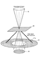
収束レンズ13、14を調整することにより、焦点位置が調整された極微小電子線プローブとなった電子線は、試料40に照射され、試料40を透過、または、試料40において散乱される。このように試料40を透過、または、試料40において散乱散乱された電子線は、投影レンズ19を介し、試料40の後段に設置されている第1の電子顕微鏡像検出器21と第2の電子顕微鏡像検出器22により検出される。第1の電子顕微鏡像検出器21は、ADF(annular dark-filed:環状暗視野)-STEM像を検出するためのものであり、中央部分に開口部21aが形成されておりリング状に形成されている。第2の電子顕微鏡像検出器22は、MABF(middle-angle bright-field:中角度領域明視野)-STEM像を検出するためのものであり、第1の電子顕微鏡像検出器21の開口部21aを通った電子線を検出する。尚、図2は、試料40に照射された電子線10と、第1の電子顕微鏡像検出器21及び第2の電子顕微鏡像検出器22との関係を示す図である。
また、本実施の形態における走査透過電子顕微鏡は、制御解析部50を有している。制御解析部50は、画像位置ずれ量算出部51、画像位置合わせ部52、画像規格化部53、画像演算部54、画像出力部55を有しており、画像出力部55より出力された画像情報は、制御解析部50に接続された表示部60に表示される。また、制御解析部50は、収束レンズ13、14、球面収差補正部17、対物レンズ18、投影レンズ19等の制御を行うとともに、第1の電子顕微鏡像検出器21及び第2の電子顕微鏡像検出器22において検出された情報に基づき解析等を行う。
(電子顕微鏡による分析方法)
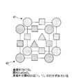
次に、本実施の形態における電子顕微鏡による分析方法について説明する。本実施の形態における電子顕微鏡による分析方法において、分析対象となる試料40は、図3に示すように、酸化物等の結晶基板からなる基板41の上に、基板41とは異なる材料を結晶成長させることにより膜42が形成されている。本実施の形態においては、基板41は、フッ素よりも軽い元素を含む材料により形成されており、例えば、酸化物、窒化物、フッ化物、炭化物等の結晶により形成されている。
次に、本実施の形態における電子顕微鏡による分析方法について説明する。本実施の形態における電子顕微鏡による分析方法において、分析対象となる試料40は、図3に示すように、酸化物等の結晶基板からなる基板41の上に、基板41とは異なる材料を結晶成長させることにより膜42が形成されている。本実施の形態においては、基板41は、フッ素よりも軽い元素を含む材料により形成されており、例えば、酸化物、窒化物、フッ化物、炭化物等の結晶により形成されている。
図1に示す本実施の形態における走査透過電子顕微鏡においては、第1の電子顕微鏡像検出器21によりADF-STEM像、第2の電子顕微鏡像検出器22によりMABF-STEM像を同時に取得することができる。一般的に、ADF-STEMは、重元素が存在している位置に強い強度が現れる観察方法であり、MABF-STEMは、軽元素が存在している位置に強い強度が現れる観察方法である。
本実施の形態における電子顕微鏡による分析方法においては、試料40における基板面に対し垂直に電子線を照射することにより原子位置の情報を取得する方法であるため、電子線の入射方向に基板41と膜42とが存在している。このため、電子線の焦点位置を膜42にした場合におけるADF-STEM像では、膜42を形成している材料に含まれる重元素の情報と基板41を形成している材料に含まれる重元素の情報とが同時に現れることがある。即ち、電子線の焦点位置を膜42にした場合には、膜42を形成している材料に含まれる重元素の情報のみならず、基板41を形成している材料に含まれる重元素の情報も同時に現れる場合があり、この場合、膜42の情報のみを得ることはできない。このことは、膜42の厚さが薄い場合により一層顕著となる。
また、MABF-STEM像は、試料40の全体において軽元素の割合が多い方の情報が顕著に現れる。よって、膜42に比べて基板41が厚い場合には、電子線の焦点位置を膜42にした場合であっても、基板41を形成している材料に含まれる軽元素の情報が主な情報として現れる。
電子線の焦点位置を基板41にした場合におけるADF-STEM像では、基板41を形成している材料に含まれる重元素の情報が現れる。また、電子線の焦点位置を膜42にした場合におけるMABF-STEM像では、基板41を形成している材料に含まれる軽元素の情報が主な情報として現れる。
ところで、上述したように、電子線の焦点位置を基板41から膜42に移動させた際には、一般的にドリフトが生じ、観察位置が原子レベルでずれてしまう。本実施の形態においては、同じ焦点位置において、ADF-STEM像とMABF-STEM像とを同時に取得するため、取得されたADF-STEM像とMABF-STEM像との間において、画像の位置ずれはない。また、MABF-STEM像の場合、焦点位置を基板41から膜42に変更しても、観察される軽元素の情報に変化はない。よって、本実施の形態においては、焦点位置が基板41の場合のMABF-STEM像と、焦点位置が膜42の場合のMABF-STEM像とに基づいて画像位置ずれの補正を行う。これにより、焦点位置が基板41の場合のADF-STEM像と、焦点位置が膜42の場合のADF-STEM像とにおいて、正確な位置合わせを行うことができる。
上述したように、焦点位置が膜42の場合におけるADF-STEM像には、膜42を形成している材料に含まれる重元素の情報と基板41を形成している材料に含まれる重元素の情報とが同時に現れることがある。電子線の焦点位置を基板41にした場合におけるADF-STEM像では、基板41を形成している材料に含まれる重元素の情報しか現れない。よって、本実施の形態においては、焦点位置が膜42の場合と、焦点位置が基板41の場合のMABF-STEM像に基づき、焦点位置が膜42の場合のADF-STEM像と、電子線の焦点位置が基板41の場合のADF-STEM像との位置合わせを行う。この後、電子線の焦点位置が基板41の場合におけるADF-STEM像から、電子線の焦点位置が膜42の場合におけるADF-STEM像を引く画像演算を行う。これにより、膜42を形成している材料に含まれる重元素の位置の情報を画像として得ることができる。
即ち、本実施の形態は、最初に、電子線の焦点位置が膜42の場合におけるMABF-STEM像とADF-STEM像と、電子線の焦点位置が基板41の場合におけるMABF-STEM像とADF-STEM像を取得する。この後、電子線の焦点位置が膜42の場合におけるADF-STEM像と、電子線の焦点位置が基板41の場合におけるADF-STEM像とにおいて、画像演算を行うことにより、膜42における画像情報を取得する分析方法である。
高分解能STEM像では、試料40にナノメートル以下に収束させた電子線を入射させ、試料40において回折させ、回折像面に設置されている環状のADF検出器(annular dark filed detector)に到達する電子の数をカウントする。このカウントされた電子の数を入射電子の位置と同期させて像の強度とする。これを収束された電子線を走査させながら行うことにより、2次元像の暗視野STEM像を得ることができる。この像は、一般的にhigh-angle annular dark-field(HAADF)-STEM像と呼ばれており、ADF-STEM像の一種である。HAADF-SETM像の特徴は、原子の位置にその原子における元素の原子番号に対応した強度が得られることにある。また、電子線を収束させる電磁レンズの焦点や試料の厚さに像のコントラストが極めて鈍感であるため、原子直視性に優れた像を取得することができる。共焦点走査透過型電子顕微鏡装置においては、像の空間分解能は収束される電子線の収束される径に依存しており、球面収差補正装置を用いた場合には、その空間分解能は1μm以下にすることができる。これらの特徴により構造解析にも広く利用されている。
本実施の形態においては、HAADF-STEM像を検出する際には、円環状の第1の電子顕微鏡像検出器21を用いている。よって、第1の電子顕微鏡像検出器21における中央部分に形成された開口部21aを通った電子線は円板状の第2の電子顕微鏡像検出器22により検出される。このように、円板状の第2の電子顕微鏡像検出器22において検出された電子線により得られた像をbright-field(BF)-STEM像と呼ぶ。円板状の第2の電子顕微鏡像検出器22の取り込み条件の設定によって、BF-STEM像の特徴は大きく変化する。取り込み角度を大きくすることによって得られた像はHAADF-STEM像の相補像として知られており、high-angle bright-field(HABF)-STEM像として分類される。また、中程度の取り込み角度(9mラジアン~12mラジアン)で取得されたBF-STEM像は、MABF-STEM像として分類され、軽元素の位置において明るくなる像が得られることが知られている。
次に、本実施の形態における電子顕微鏡による分析方法について行ったシミュレーションに基づき説明する。シミュレーションにおいては、試料40として、基板41にはSrTiO3の結晶基板を用い、この結晶基板である基板41の上に、LaCoO3を結晶成長成長させた結晶膜となる膜42が形成されている構造のモデルを用いた。また、試料40のモデルにおいては、基板41の厚さを68nmとし、膜42の厚さを12nmとし、基板41と膜42における原子位置は、単位格子を基準として(1/4 1/4 0)だけずらしたものである。電子線の入射方位は[0 0 1]方向とし、3次元断層像を取得する方法は、特許文献1に開示されている方法と同様である。尚、特許文献1に開示されている方法は、球面収差補正された電磁レンズで形成される電子線は、焦点深度が極めて浅くなっており、観察対象となる部分に焦点が位置するように電磁レンズの焦点を変化させて像を得ている。
図5に示すように、電子線の焦点位置が膜42となる場合は、表面より深さ方向に5nm深い位置に焦点が位置するようにデフォーカスさせた状態において計算を行った。また、電子線の焦点位置が基板41となる場合は、表面より深さ方向に30nm深い位置に焦点が位置するようにデフォーカスさせた状態において計算を行った。図6(a)及び(b)は、電子線の焦点位置が膜42の場合のものである。具体的には、図6(a)は、試料40における膜42側の表面より深さ方向に5nm深い位置を電子線の焦点位置とした場合におけるMABF-STEM像であり、図6(b)は、この場合におけるADF-STEM像である。図6(c)及び(d)は、電子線の焦点位置が基板41の場合のものである。具体的には、図6(c)は、試料40における膜42側の表面より深さ方向に30nm深い位置を電子線の焦点位置とした場合におけるMABF-STEM像であり、図6(d)は、この場合におけるADF-STEM像である。
本実施の形態においては、図6(a)に示されるMABF-STEM像を第1の電子顕微鏡像と記載し、図6(b)に示されるADF-STEM像を第2の電子顕微鏡像と記載する場合がある。また、図6(c)に示されるMABF-STEM像を第3の電子顕微鏡像と記載し、図6(d)に示されるADF-STEM像を第4の電子顕微鏡像と記載する場合がある。
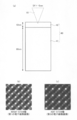
次に、得られたSTEM像についてより詳細に説明する。図7(a)は、電子線の焦点位置が膜42の場合、即ち、試料40の表面より深さ方向に5nm深い位置を電子線の焦点位置とした場合の様子を示すものである。図7(b)は、この場合において得られるMABF-STEM像(第1の電子顕微鏡像)であり、図7(c)はADF-STEM像(第2の電子顕微鏡像)である。図7(b)に示されるMABF-STEM像(第1の電子顕微鏡像)では、基板41における軽元素の位置、即ち、基板41を形成しているSrTiO3における酸素(O)の位置が最も明るく示されている。また、図7(c)に示されるADF-STEM像(第2の電子顕微鏡像)では、基板41における重元素と膜42における重元素の位置が明るく示されている。即ち、基板41を形成しているSrTiO3におけるSr及びTiの位置、膜42を形成しているLaCoO3におけるLa及びCoの位置が明るく示されている。これは、図7(c)に示されるADF-STEM像(第2の電子顕微鏡像)では、電子線の焦点位置に存在する重元素から散乱される熱散漫散乱電子を検出しているため、焦点位置における重元素が像に主に現れている。一方、図7(b)に示されるMABF-STEM像(第1の電子顕微鏡像)では、試料40全体において、軽元素が最も多い位置が明るくなるからである。
図8(a)は、電子線の焦点位置が基板の場合、即ち、試料40の表面より深さ方向に30nm深い位置を電子線の焦点位置とした場合の様子を示すものである。図8(b)は、この場合において得られるMABF-STEM像(第3の電子顕微鏡像)であり、図8(c)はADF-STEM像(第4の電子顕微鏡像)である。図8(b)に示されるMABF-STEM像(第3の電子顕微鏡像)では、基板41における軽元素の位置、即ち、基板41を形成しているSrTiO3における酸素(O)の位置が最も明るく示されている。また、図8(c)に示されるADF-STEM像(第4の電子顕微鏡像)では、基板41における重元素、即ち、基板41を形成しているSrTiO3におけるSr及びTiの位置が明るく示されている。
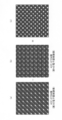
本実施の形態においては、最初に、電子線の焦点位置が膜42の場合におけるMABF-STEM像(第1の電子顕微鏡像)と電子線の焦点位置が基板41の場合におけるMABF-STEM像(第3の電子顕微鏡像)とにより画像位置ずれ量を算出する。この後、電子線の焦点位置が膜42の場合におけるADF-STEM像(第2の電子顕微鏡像)と電子線の焦点位置が基板41の場合におけるADF-STEM像(第4の電子顕微鏡像)とを算出されたずれ量だけ相対的にずらす。これにより、電子線の焦点位置が膜42の場合におけるADF-STEM像(第2の電子顕微鏡像)と電子線の焦点位置が基板41の場合におけるADF-STEM像(第4の電子顕微鏡像)との位置を一致させることができる。この後、電子線の焦点位置が膜42の場合におけるADF-STEM像(第2の電子顕微鏡像)及び電子線の焦点位置が基板41の場合におけるADF-STEM像(第4の電子顕微鏡像)において、画像の明るさを規格化する。この後、図9(a)に示される電子線の焦点位置が膜42の場合におけるADF-STEM像(第2の電子顕微鏡像)から、図9(b)に示される電子線の焦点位置が基板41の場合におけるADF-STEM像(第4の電子顕微鏡像)を引く画像演算を行う。これにより、図9(c)に示されるような、膜42における構造、即ち、膜42を形成しているLaCoO3における重元素であるLa及びCoの位置が示された画像を得ることができる。
尚、電子線の焦点位置が膜42の場合におけるMABF-STEM像と電子線の焦点位置が基板41の場合におけるMABF-STEM像とにより画像位置ずれ量を算出する方法としては、相関法や位相相関限定法等を用いることができる。
次に、本実施の形態における電子顕微鏡を用いた分析方法について、図10に示すフローチャートに基づき説明する。
最初に、ステップ102(S102)において、電子線の焦点位置が膜42の場合におけるADF-STEM像(第1の電子顕微鏡像)及びMABF-STEM像(第2の電子顕微鏡像)を取得する。具体的には、電子線の焦点位置が試料40の膜42に位置するように調整して電子線を照射し、試料40を透過、または、試料40において散乱された電子線を第1の電子顕微鏡像検出器21及び第2の電子顕微鏡像検出器22において検出する。これにより、第1の電子顕微鏡像検出器21により、電子線の焦点位置が膜42の場合におけるADF-STEM像(第1の電子顕微鏡像)が検出される。また、第2の電子顕微鏡像検出器22により、電子線の焦点位置が膜42の場合におけるMABF-STEM像(第2の電子顕微鏡像)が検出される。
次に、ステップ104(S104)において、電子線の焦点位置が基板41の場合におけるADF-STEM像(第3の電子顕微鏡像)及びMABF-STEM像(第4の電子顕微鏡像)を取得する。具体的には、電子線の焦点位置が試料40の基板41に位置するように調整して電子線を照射し、試料40を透過、または、試料40において散乱された電子線を第1の電子顕微鏡像検出器21及び第2の電子顕微鏡像検出器22において検出する。これにより、第1の電子顕微鏡像検出器21により、電子線の焦点位置が基板41の場合におけるADF-STEM像(第3の電子顕微鏡像)が検出される。また、第2の電子顕微鏡像検出器22により、電子線の焦点位置が基板41の場合におけるMABF-STEM像(第4の電子顕微鏡像)が検出される。
次に、ステップ106(S106)において、電子線の焦点位置が膜42の場合と電子線の焦点位置が基板41の場合における画像位置ずれ量を算出する。具体的には、制御解析部50における画像位置ずれ量算出部51に、電子線の焦点位置が膜42の場合におけるMABF-STEM像(第1の電子顕微鏡像)と電子線の焦点位置が基板41の場合におけるMABF-STEM像(第3の電子顕微鏡像)とを入力する。この後、画像位置ずれ量算出部51において、電子線の焦点位置が膜42の場合におけるMABF-STEM像(第1の電子顕微鏡像)と電子線の焦点位置が基板41の場合におけるMABF-STEM像(第3の電子顕微鏡像)に基づき画像位置ずれ量を算出する。
次に、ステップ108(S108)において、電子線の焦点位置が膜42の場合におけるADF-STEM像(第2の電子顕微鏡像)と、電子線の焦点位置が基板41の場合におけるADF-STEM像(第4の電子顕微鏡像)との位置合わせを行う。即ち、ステップ106において算出された画像位置ずれ量に基づき、電子線の焦点位置が膜42の場合におけるADF-STEM像(第2の電子顕微鏡像)に対し、電子線の焦点位置が基板41の場合におけるADF-STEM像(第4の電子顕微鏡像)を動かす。この工程は、画像位置合わせ部52において行われる。これにより、電子線の焦点位置が膜42の場合におけるADF-STEM像(第2の電子顕微鏡像)と、電子線の焦点位置が基板41の場合におけるADF-STEM像(第4の電子顕微鏡像)との位置合わせを行うことができる。このようにして、電子線の焦点位置が膜42の場合におけるADF-STEM像(第2の電子顕微鏡像)の位置と、電子線の焦点位置が基板41の場合におけるADF-STEM像(第4の電子顕微鏡像)の位置とを一致させることができる。
次に、ステップ110(S110)において、電子線の焦点位置が膜42の場合におけるADF-STEM像(第2の電子顕微鏡像)と電子線の焦点位置が基板41の場合におけるADF-STEM像(第4の電子顕微鏡像)との明るさの強度の規格化を行う。この規格化は、画像規格化部53において行われる。具体的には、電子線の焦点位置が膜42の場合におけるADF-STEM像(第2の電子顕微鏡像)と、電子線の焦点位置が基板41の場合におけるADF-STEM像(第4の電子顕微鏡像)とにおいて、基板41における重元素の明るさを略一致させる。
次に、ステップ112(S112)において、電子線の焦点位置が膜42の場合におけるADF-STEM像(第2の電子顕微鏡像)より電子線の焦点位置が基板41の場合におけるADF-STEM像(第4の電子顕微鏡像)を引く画像演算を行う。これにより、膜42における画像を得る。具体的には、画像演算部54において、電子線の焦点位置が膜42の場合におけるADF-STEM像(第2の電子顕微鏡像)から電子線の焦点位置が基板41の場合におけるADF-STEM像(第4の電子顕微鏡像)を引く画像演算を行う。この画像演算により得られた膜42における画像は、画像出力部55を介し、表示部60に表示される。これにより、膜42が、LaCoO3により形成されている場合には、膜42を形成しているLaCoO3の構造、即ち、LaCoO3におけるLa及びCoの位置を知ることができる。
(実施例)
次に、本実施の形態における実施例について説明する。本実施例において用いた試料40は、基板41には、SrTiO3(0 0 1)基板が用いられており、膜42には、歪みを含んだLaCoO3成長膜が形成されている。
次に、本実施の形態における実施例について説明する。本実施例において用いた試料40は、基板41には、SrTiO3(0 0 1)基板が用いられており、膜42には、歪みを含んだLaCoO3成長膜が形成されている。
図11は、電子線の焦点位置が膜42の場合におけるADF-STEM像(第2の電子顕微鏡像)であり、図11は、電子線の焦点位置が基板41の場合におけるADF-STEM像(第4の電子顕微鏡像)である。本実施例では、最初に電子線の焦点位置が膜42の場合におけるMABF-STEM像(第1の電子顕微鏡像)と電子線の焦点位置が基板41の場合におけるMABF-STEM像(第3の電子顕微鏡像)に基づき、相互の画像における画像位置ずれ量を算出する。次に、電子線の焦点位置が膜42の場合におけるADF-STEM像(第2の電子顕微鏡像)と電子線の焦点位置が基板41の場合におけるADF-STEM像(第4の電子顕微鏡像)との間で位置合わせを行う。次に、電子線の焦点位置が膜42の場合におけるADF-STEM像(第2の電子顕微鏡像)と電子線の焦点位置が基板41の場合におけるADF-STEM像(第4の電子顕微鏡像)とにおいて、画像の明るさを均一にする規格化を行う。次に、電子線の焦点位置が膜42の場合におけるADF-STEM像(第2の電子顕微鏡像)より電子線の焦点位置が基板41の場合におけるADF-STEM像(第4の電子顕微鏡像)を引く画像演算を行う。これにより、図13に示すように、基板41に成膜されている膜42であるLaCoO3成長膜の画像を得ることができる。このようにして得られた図13に示す画像において、FFT(Fast Fourier Transform)を行った画像を図14に示す。
このように、本実施例に示されるように、基板41に成膜されている膜42における原子配列の画像を得ることができ、基板41に成膜されている膜42における歪み等を容易に知ることが可能となる。
以上、実施の形態について詳述したが、特定の実施形態に限定されるものではなく、特許請求の範囲に記載された範囲内において、種々の変形及び変更が可能である。
10 電子線
11 電界放射型電子銃
12 加速部
13 収束レンズ
14 収束レンズ
15 収束レンズ絞り
16 走査コイル
17 球面収差補正部
18 対物レンズ
19 投影レンズ
21 第1の電子顕微鏡像検出器
22 第2の電子顕微鏡像検出器
40 試料
41 基板
42 膜
50 制御解析部
51 画像位置ずれ量算出部
52 画像位置合わせ部
53 画像規格化部
54 画像演算部
55 画像出力部
60 表示部
11 電界放射型電子銃
12 加速部
13 収束レンズ
14 収束レンズ
15 収束レンズ絞り
16 走査コイル
17 球面収差補正部
18 対物レンズ
19 投影レンズ
21 第1の電子顕微鏡像検出器
22 第2の電子顕微鏡像検出器
40 試料
41 基板
42 膜
50 制御解析部
51 画像位置ずれ量算出部
52 画像位置合わせ部
53 画像規格化部
54 画像演算部
55 画像出力部
60 表示部
Claims (10)
- 電子源より放出された電子線を加速し、試料に前記電子線の焦点が位置するように照射して、前記試料を透過または前記試料により散乱された電子線を検出することにより前記試料における環状暗視野像を検出する第1の電子顕微鏡像検出器と、前記試料における中角度領域明視野像を検出する第2の電子顕微鏡像検出器とを有する電子顕微鏡による分析方法において、
前記試料は基板の表面に膜が形成されており、
前記基板は、フッ素またはフッ素よりも軽い元素を含むものであって、
前記試料における前記膜に、前記電子線の焦点が位置するように電子線を照射し、前記第1の電子顕微鏡像検出器により第1の電子顕微鏡像、前記第2の電子顕微鏡像検出器により第2の電子顕微鏡像を取得する工程と、
前記試料における前記基板に、前記電子線の焦点が位置するように電子線を照射し、前記第1の電子顕微鏡像検出器により第3の電子顕微鏡像、前記第2の電子顕微鏡像検出器により第4の電子顕微鏡像を取得する工程と、
前記第1の電子顕微鏡像と前記第3の電子顕微鏡像に基づき、前記第2の電子顕微鏡像と前記第4の電子顕微鏡像との位置合わせを行う工程と、
前記位置合わせを行う工程の後、前記第2の電子顕微鏡像より前記第4の電子顕微鏡像を引く画像演算を行う工程と、
を有することを特徴とする電子顕微鏡による分析方法。 - 前記位置合わせを行う工程は、
前記第1の電子顕微鏡像における画像と前記第3の電子顕微鏡像における画像との画像位置ずれ量を算出する工程と、
前記第2の電子顕微鏡像または前記第4の電子顕微鏡像を前記算出された画像位置ずれ量動かすことにより、前記第2の電子顕微鏡像と前記第4の電子顕微鏡像との位置合わせを行う工程と、
を有することを特徴とする請求項1に記載の電子顕微鏡による分析方法。 - 前記画像位置ずれ量を算出する工程は、前記第1の電子顕微鏡像におけるフッ素またはフッ素よりも軽い元素の位置と、前記第3の電子顕微鏡像におけるフッ素またはフッ素よりも軽い元素の位置とのずれ量を算出することにより行われるものであることを特徴とする請求項2に記載の電子顕微鏡による分析方法。
- 前記位置合わせを行う工程の後、前記画像演算を行う工程の前に、
前記第2の電子顕微鏡像と前記第4の電子顕微鏡像とにおける明るさを均一にする工程を有することを特徴とする請求項1から3のいずれかに記載の電子顕微鏡による分析方法。 - 前記電子源と前記試料との間には、対物レンズが設けられており、
前記電子源と前記対物レンズとの間には、前記電子線の球面収差を補正する球面収差補正部が設けられていることを特徴とする請求項1から4のいずれかに記載の電子顕微鏡による分析方法。 - 前記試料において前記電子線を走査することを特徴とする請求項1から5のいずれかに記載の電子顕微鏡による分析方法。
- 電子線を放出する電子源と、
前記電子源より放出された前記電子線を加速する加速部と、
前記加速部により加速された電子線の焦点を試料に結ぶ対物レンズと、
前記試料を透過または前記試料において散乱された電子線を検出することにより、前記試料における環状暗視野像を検出する中央部分に開口部を有する環状に形成された第1の電子顕微鏡像検出器と、
前記第1の電子顕微鏡像検出器における開口部を通った電子線を検出することにより、前記試料における中角度領域明視野像を検出する第2の電子顕微鏡像検出器と、
を有し、
前記試料は基板の表面に膜が形成されており、
前記基板は、フッ素またはフッ素よりも軽い元素を含むものであって、
前記試料における前記膜に、前記電子線の焦点が位置するように電子線を照射し、前記第1の電子顕微鏡像検出器により第1の電子顕微鏡像、前記第2の電子顕微鏡像検出器により第2の電子顕微鏡像を取得し、
前記試料における前記基板に、前記電子線の焦点が位置するように電子線を照射し、前記第1の電子顕微鏡像検出器により第3の電子顕微鏡像、前記第2の電子顕微鏡像検出器により第4の電子顕微鏡像を取得するものであって、
前記第1の電子顕微鏡像における画像と前記第3の電子顕微鏡像における画像との画像位置ずれ量を算出する画像位置ずれ量算出部と、
前記算出された画像位置ずれ量に基づき前記第2の電子顕微鏡像と前記第4の電子顕微鏡像との位置合わせを行う画像位置合わせ部と、
前記位置合わせのなされた前記第2の電子顕微鏡像より前記第4の電子顕微鏡像を引く画像演算を行う画像演算部と、
を有することを特徴とする電子顕微鏡。 - 前記第2の電子顕微鏡像と前記第4の電子顕微鏡像とにおける明るさを均一にする画像規格化部を有することを特徴とする請求項7に記載の電子顕微鏡。
- 前記電子源と前記対物レンズとの間には、前記電子線の球面収差を補正する球面収差補正部が設けられていることを特徴とする請求項7または8に記載の電子顕微鏡。
- 前記試料において前記電子線を走査する電子線走査部を有することを特徴とする請求項7から9のいずれかに記載の電子顕微鏡。
Priority Applications (3)
| Application Number | Priority Date | Filing Date | Title |
|---|---|---|---|
| PCT/JP2014/064530 WO2015181981A1 (ja) | 2014-05-30 | 2014-05-30 | 電子顕微鏡による分析方法及び電子顕微鏡 |
| JP2016523083A JP6213674B2 (ja) | 2014-05-30 | 2014-05-30 | 電子顕微鏡による分析方法及び電子顕微鏡 |
| US15/247,133 US9748073B2 (en) | 2014-05-30 | 2016-08-25 | Analysis method using electron microscope, and electron microscope |
Applications Claiming Priority (1)
| Application Number | Priority Date | Filing Date | Title |
|---|---|---|---|
| PCT/JP2014/064530 WO2015181981A1 (ja) | 2014-05-30 | 2014-05-30 | 電子顕微鏡による分析方法及び電子顕微鏡 |
Related Child Applications (1)
| Application Number | Title | Priority Date | Filing Date |
|---|---|---|---|
| US15/247,133 Continuation US9748073B2 (en) | 2014-05-30 | 2016-08-25 | Analysis method using electron microscope, and electron microscope |
Publications (1)
| Publication Number | Publication Date |
|---|---|
| WO2015181981A1 true WO2015181981A1 (ja) | 2015-12-03 |
Family
ID=54698354
Family Applications (1)
| Application Number | Title | Priority Date | Filing Date |
|---|---|---|---|
| PCT/JP2014/064530 Ceased WO2015181981A1 (ja) | 2014-05-30 | 2014-05-30 | 電子顕微鏡による分析方法及び電子顕微鏡 |
Country Status (3)
| Country | Link |
|---|---|
| US (1) | US9748073B2 (ja) |
| JP (1) | JP6213674B2 (ja) |
| WO (1) | WO2015181981A1 (ja) |
Cited By (1)
| Publication number | Priority date | Publication date | Assignee | Title |
|---|---|---|---|---|
| JP2018179726A (ja) * | 2017-04-12 | 2018-11-15 | 富士通株式会社 | 分析方法及び分析装置 |
Families Citing this family (1)
| Publication number | Priority date | Publication date | Assignee | Title |
|---|---|---|---|---|
| KR102224466B1 (ko) * | 2018-11-07 | 2021-03-05 | 포항공과대학교 산학협력단 | 기계학습을 이용한 페로브스카이트의 구조 분석 방법 |
Citations (1)
| Publication number | Priority date | Publication date | Assignee | Title |
|---|---|---|---|---|
| JP2013041761A (ja) * | 2011-08-17 | 2013-02-28 | Fujitsu Ltd | 画像処理装置、像を生成する方法並びにシステム |
Family Cites Families (6)
| Publication number | Priority date | Publication date | Assignee | Title |
|---|---|---|---|---|
| JP2010251041A (ja) | 2009-04-14 | 2010-11-04 | Renesas Electronics Corp | 走査型透過電子顕微鏡 |
| JP5390926B2 (ja) | 2009-04-28 | 2014-01-15 | 日本電子株式会社 | 環状明視野像観察装置 |
| JP5502407B2 (ja) * | 2009-09-17 | 2014-05-28 | 日本電子株式会社 | 共焦点stem像取得方法及び装置 |
| JP5499282B2 (ja) * | 2010-07-16 | 2014-05-21 | 国立大学法人 東京大学 | 走査透過電子顕微鏡における収差補正方法および収差補正装置 |
| JP5423612B2 (ja) | 2010-08-16 | 2014-02-19 | 富士通株式会社 | 共焦点走査透過型電子顕微鏡装置及び3次元断層像観察方法 |
| JP5712074B2 (ja) * | 2011-07-20 | 2015-05-07 | 株式会社日立ハイテクノロジーズ | 走査透過電子顕微鏡 |
-
2014
- 2014-05-30 JP JP2016523083A patent/JP6213674B2/ja not_active Expired - Fee Related
- 2014-05-30 WO PCT/JP2014/064530 patent/WO2015181981A1/ja not_active Ceased
-
2016
- 2016-08-25 US US15/247,133 patent/US9748073B2/en not_active Expired - Fee Related
Patent Citations (1)
| Publication number | Priority date | Publication date | Assignee | Title |
|---|---|---|---|---|
| JP2013041761A (ja) * | 2011-08-17 | 2013-02-28 | Fujitsu Ltd | 画像処理装置、像を生成する方法並びにシステム |
Cited By (1)
| Publication number | Priority date | Publication date | Assignee | Title |
|---|---|---|---|---|
| JP2018179726A (ja) * | 2017-04-12 | 2018-11-15 | 富士通株式会社 | 分析方法及び分析装置 |
Also Published As
| Publication number | Publication date |
|---|---|
| US9748073B2 (en) | 2017-08-29 |
| JPWO2015181981A1 (ja) | 2017-04-20 |
| JP6213674B2 (ja) | 2017-10-18 |
| US20160365220A1 (en) | 2016-12-15 |
Similar Documents
| Publication | Publication Date | Title |
|---|---|---|
| JP5712074B2 (ja) | 走査透過電子顕微鏡 | |
| US6750451B2 (en) | Observation apparatus and observation method using an electron beam | |
| US20070158567A1 (en) | Apparatus and adjusting method for a scanning transmission electron microscope | |
| US9224574B2 (en) | Charged particle optical equipment and method for measuring lens aberration | |
| JP5315033B2 (ja) | 電子分光器を備えた透過型電子顕微鏡 | |
| JP4790567B2 (ja) | ロンチグラムを用いた収差測定方法及び収差補正方法及び電子顕微鏡 | |
| JP2006173027A (ja) | 走査透過電子顕微鏡、及び収差測定方法、ならびに収差補正方法 | |
| JP5423612B2 (ja) | 共焦点走査透過型電子顕微鏡装置及び3次元断層像観察方法 | |
| JP2007157719A (ja) | 粒子光学レンズの収差関数における収差係数の決定方法 | |
| JP6876418B2 (ja) | 画像取得方法および電子顕微鏡 | |
| CN110310877B (zh) | 用于自动对准扫描透射电子显微镜的方法 | |
| JP6213674B2 (ja) | 電子顕微鏡による分析方法及び電子顕微鏡 | |
| JP2011258576A (ja) | 荷電粒子線装置に用いられる標準試料,荷電粒子線装置、及び荷電粒子線装置に用いられる標準試料の製造方法 | |
| JP5817360B2 (ja) | 走査透過型電子顕微鏡の観察方法及び走査透過型電子顕微鏡 | |
| CN106645250B (zh) | 一种具备光学成像功能的扫描透射电子显微镜 | |
| JP5934513B2 (ja) | 透過電子顕微鏡 | |
| JP2016039118A (ja) | 電子顕微鏡、およびモノクロメーターの調整方法 | |
| JP5147567B2 (ja) | 電子分光器を有する透過型電子顕微鏡装置,試料ホルダ,試料台及びスペクトル像の取得方法 | |
| JP4337832B2 (ja) | 電子線を用いた観察装置及び観察方法 | |
| JP6962757B2 (ja) | 測定方法および電子顕微鏡 | |
| JP6318986B2 (ja) | 走査透過型電子顕微鏡像の取得方法及び走査透過型電子顕微鏡 | |
| JP5470408B2 (ja) | 電子分光器を有する透過型電子顕微鏡装置,試料ホルダ,試料台及びスペクトル像の取得方法 | |
| JPWO2007125652A1 (ja) | 電子顕微鏡とその対物レンズ系収差特性の計測方法 | |
| JP2016009622A (ja) | 電子顕微鏡における検出器の位置調整方法及び画像検出器の位置調整方法 | |
| JP2014082134A (ja) | 電子装置及び電子線を照射する方法 |
Legal Events
| Date | Code | Title | Description |
|---|---|---|---|
| 121 | Ep: the epo has been informed by wipo that ep was designated in this application |
Ref document number: 14893352 Country of ref document: EP Kind code of ref document: A1 |
|
| ENP | Entry into the national phase |
Ref document number: 2016523083 Country of ref document: JP Kind code of ref document: A |
|
| NENP | Non-entry into the national phase |
Ref country code: DE |
|
| 122 | Ep: pct application non-entry in european phase |
Ref document number: 14893352 Country of ref document: EP Kind code of ref document: A1 |