WO2015166687A1 - 検出装置およびそれを備えた電子機器、ならびに検出装置の制御方法 - Google Patents
検出装置およびそれを備えた電子機器、ならびに検出装置の制御方法 Download PDFInfo
- Publication number
- WO2015166687A1 WO2015166687A1 PCT/JP2015/054361 JP2015054361W WO2015166687A1 WO 2015166687 A1 WO2015166687 A1 WO 2015166687A1 JP 2015054361 W JP2015054361 W JP 2015054361W WO 2015166687 A1 WO2015166687 A1 WO 2015166687A1
- Authority
- WO
- WIPO (PCT)
- Prior art keywords
- position detection
- electrode group
- period
- self
- capacitance method
- Prior art date
- Legal status (The legal status is an assumption and is not a legal conclusion. Google has not performed a legal analysis and makes no representation as to the accuracy of the status listed.)
- Ceased
Links
Images












Classifications
-
- G—PHYSICS
- G06—COMPUTING OR CALCULATING; COUNTING
- G06F—ELECTRIC DIGITAL DATA PROCESSING
- G06F3/00—Input arrangements for transferring data to be processed into a form capable of being handled by the computer; Output arrangements for transferring data from processing unit to output unit, e.g. interface arrangements
- G06F3/01—Input arrangements or combined input and output arrangements for interaction between user and computer
- G06F3/03—Arrangements for converting the position or the displacement of a member into a coded form
- G06F3/041—Digitisers, e.g. for touch screens or touch pads, characterised by the transducing means
- G06F3/0416—Control or interface arrangements specially adapted for digitisers
- G06F3/04166—Details of scanning methods, e.g. sampling time, grouping of sub areas or time sharing with display driving
- G06F3/041662—Details of scanning methods, e.g. sampling time, grouping of sub areas or time sharing with display driving using alternate mutual and self-capacitive scanning
-
- G—PHYSICS
- G06—COMPUTING OR CALCULATING; COUNTING
- G06F—ELECTRIC DIGITAL DATA PROCESSING
- G06F3/00—Input arrangements for transferring data to be processed into a form capable of being handled by the computer; Output arrangements for transferring data from processing unit to output unit, e.g. interface arrangements
- G06F3/01—Input arrangements or combined input and output arrangements for interaction between user and computer
- G06F3/03—Arrangements for converting the position or the displacement of a member into a coded form
- G06F3/041—Digitisers, e.g. for touch screens or touch pads, characterised by the transducing means
- G06F3/0412—Digitisers structurally integrated in a display
-
- G—PHYSICS
- G06—COMPUTING OR CALCULATING; COUNTING
- G06F—ELECTRIC DIGITAL DATA PROCESSING
- G06F3/00—Input arrangements for transferring data to be processed into a form capable of being handled by the computer; Output arrangements for transferring data from processing unit to output unit, e.g. interface arrangements
- G06F3/01—Input arrangements or combined input and output arrangements for interaction between user and computer
- G06F3/03—Arrangements for converting the position or the displacement of a member into a coded form
- G06F3/041—Digitisers, e.g. for touch screens or touch pads, characterised by the transducing means
- G06F3/0416—Control or interface arrangements specially adapted for digitisers
- G06F3/0418—Control or interface arrangements specially adapted for digitisers for error correction or compensation, e.g. based on parallax, calibration or alignment
- G06F3/04184—Synchronisation with the driving of the display or the backlighting unit to avoid interferences generated internally
-
- G—PHYSICS
- G06—COMPUTING OR CALCULATING; COUNTING
- G06F—ELECTRIC DIGITAL DATA PROCESSING
- G06F3/00—Input arrangements for transferring data to be processed into a form capable of being handled by the computer; Output arrangements for transferring data from processing unit to output unit, e.g. interface arrangements
- G06F3/01—Input arrangements or combined input and output arrangements for interaction between user and computer
- G06F3/03—Arrangements for converting the position or the displacement of a member into a coded form
- G06F3/041—Digitisers, e.g. for touch screens or touch pads, characterised by the transducing means
- G06F3/044—Digitisers, e.g. for touch screens or touch pads, characterised by the transducing means by capacitive means
- G06F3/0446—Digitisers, e.g. for touch screens or touch pads, characterised by the transducing means by capacitive means using a grid-like structure of electrodes in at least two directions, e.g. using row and column electrodes
-
- G—PHYSICS
- G06—COMPUTING OR CALCULATING; COUNTING
- G06F—ELECTRIC DIGITAL DATA PROCESSING
- G06F2203/00—Indexing scheme relating to G06F3/00 - G06F3/048
- G06F2203/041—Indexing scheme relating to G06F3/041 - G06F3/045
- G06F2203/04106—Multi-sensing digitiser, i.e. digitiser using at least two different sensing technologies simultaneously or alternatively, e.g. for detecting pen and finger, for saving power or for improving position detection
Definitions
- the present invention relates to a detection device having, for example, a touch panel, and more particularly to a detection device that is used integrally with a display device and can perform position detection by both a self-capacitance method and a mutual capacitance method.
- a touch panel has been attracting attention as an input device for performing operations in a computer system or the like.
- a capacitive touch panel the position of an object to be detected such as a user (operator) finger or a touch pen is detected based on a change in capacitance.
- a capacitive touch panel is generally used integrally with a display device such as a liquid crystal display device.
- a device including a touch panel and a controller (touch panel controller) that controls the operation of the touch panel is referred to as a “detection device”.
- the self-capacitance method and the mutual capacitance method are known as the position detection method by the electrostatic capacity method.
- the self-capacitance method is a method of measuring the position of the detected object by detecting that the capacitance has increased due to the contact or approach of the detected object to the touch panel.
- the mutual capacitance method is a method of measuring the position of the detected object based on the difference in capacitance between adjacent sensors caused by the contact or approach of the detected object to the touch panel.
- a high-performance detection device examples include a hover function, a pen input function, a high-speed response function, a low power consumption function, a water droplet malfunction prevention function, and a multi-touch function.
- functions are provided in recent detection devices.
- display devices high resolution and thinning are remarkable.
- the touch panel it is conventionally known that it is susceptible to noise from the display device.
- a high-sensitivity capacitive touch panel is particularly susceptible to noise, and an unintended malfunction is caused when the drive of the touch panel and the drive of the display device interfere with each other.
- the presence of such interference also reduces the position detection accuracy. Therefore, in order to prevent malfunctions and improve the accuracy of position detection, it has been proposed to perform position detection during a period in which driving of the display device is stopped (hereinafter referred to as “pause period”). .
- Japanese Patent Laid-Open No. 2013-168083 discloses an invention of a detection device that can freely switch a signal for controlling timing (scan timing) sensed by a sensing unit (touch panel). According to the present invention, the sensing timing can be changed according to the operation status of the display device, and the detection accuracy is improved.
- the driving period of the touch panel (the period during which the touch panel can be driven without causing interference) is shortened.
- the length of the driving period is represented by an arrow 91 and the length of the rest period (the period during which the touch panel can be driven) is 92.
- the length of the drive period is represented by an arrow 93 and the length of the rest period is represented by an arrow 94.
- the driving period of the touch panel becomes shorter.
- the drive period of the touch panel is shortened to avoid interference, the performance of the touch panel is not sufficiently exhibited.
- an object of the present invention is to realize a detection device that can sufficiently exhibit performance even when used integrally with a high-resolution display device (a display device having a relatively short pause period).
- a first aspect of the present invention is a detection apparatus capable of performing position detection processing, which is processing for detecting a position where a detection target object is in contact with or approached, in both a self-capacitance method and a mutual capacitance method.
- a sensing unit having a position detection electrode group formed in a region where position detection is to be performed by the position detection process;
- a detection control unit that drives the position detection electrode group to perform the position detection process;
- the detection control unit drives the position detection electrode group based on a synchronization signal when the position detection processing is performed by at least one of a self-capacitance method and a mutual capacitance method.
- the position detection electrode group is formed in a region corresponding to an image display unit of an external display device,
- the display device is used integrally with the display device.
- the detection control unit is configured such that both the position detection process using the self-capacitance method and the position detection process using the mutual capacitance method are performed during a pause period in which the operation of the display device is stopped.
- the position detection electrode group is driven.
- the detection control unit In the horizontal blanking period of the display device, the position detection electrode group is driven based on the synchronization signal so that the position detection process in the first method is performed, In the vertical blanking period of the display device, the position detection electrode group is driven based on the synchronization signal so that the position detection processing in the second method is performed.
- the detection control unit is configured such that one of the position detection process in the self-capacitance method and the position detection process in the mutual capacitance method is performed in a pause period in which the operation of the display device is stopped.
- the position detection electrode group is driven.
- a sixth aspect of the present invention is the fifth aspect of the present invention,
- one of the self-capacitance method and the mutual capacitance method is defined as the first method and the other is defined as the second method
- the detection control unit In the horizontal blanking period of the display device, the position detection electrode group is driven based on the synchronization signal so that the position detection process in the first method is performed, In the period other than the horizontal blanking period of the display device, the position detection electrode group is driven so that the position detection process in the second method is performed.
- the detection control unit In the vertical blanking period of the display device, the position detection electrode group is driven based on the synchronization signal so that the position detection processing in the first method is performed, In the period other than the vertical blanking period of the display device, the position detection electrode group is driven so that the position detection process in the second method is performed.
- the detection control unit is configured to execute the position detection process in the self-capacitance method, the presence / absence of the position detection process in the mutual capacitance method, and the position detection process in the self-capacitance method.
- the period in which the position detection process is performed and whether or not the synchronization signal is used, and the period in which the position detection process is performed and the presence or absence of the use of the synchronization signal when the position detection process in the mutual capacitance method is performed An electrode group driving method which is a method specified by a combination and which drives the position detection electrode group can be switched during the operation of the display device.
- a ninth aspect of the present invention is the eighth aspect of the present invention,
- the detection control unit switches the electrode group driving method according to a function to be executed.
- a first driving method corresponding to an initial state and a second driving method corresponding to at least one specific function are prepared in advance.
- the detection control unit switches the electrode group driving method from the first driving method to the second driving method at the start of execution of the specific function, and drives the electrode group at the end of execution of the specific function.
- the system is switched from the second driving system to the first driving system.
- An eleventh aspect of the present invention is the eighth aspect of the present invention,
- the detection control unit switches a synchronization signal to be used according to the electrode group driving method.
- a twelfth aspect of the present invention is an electronic apparatus configured by integrating a display device having an image display unit and a detection device according to the first aspect of the present invention, The position detection electrode group is formed in a region corresponding to the image display unit, The synchronization signal is provided from the display device to the detection control unit.
- a thirteenth aspect of the present invention is a control method for a detection apparatus capable of performing a position detection process, which is a process of detecting a position where a detection object is in contact with or approaching, using both a self-capacitance method and a mutual capacitance method.
- a mutual capacitance method detection step for driving the position detection electrode group so that the position detection processing is performed in a mutual capacitance method In at least one of the self-capacitance method detection step and the mutual capacitance method detection step, the position detection electrode group is driven based on a synchronization signal.
- a fourteenth aspect of the present invention is the thirteenth aspect of the present invention,
- the method further includes an electrode group driving method switching step of switching an electrode group driving method which is a method of driving the position detection electrode group.
- the position detection electrode group is driven based on the synchronization signal.
- pause period for example, horizontal blanking period
- position detection processing can be performed during the vertical blanking period. Therefore, by performing the position detection process for realizing the function having a large influence of noise during the pause period of the display device, it is possible to prevent the malfunction caused by the noise from the display device.
- a detection device that can sufficiently exhibit performance even when used integrally with a high-resolution display device is realized.
- both the position detection process based on the self-capacitance method and the position detection process based on the mutual capacitance method are performed during the suspension period of the display device. For this reason, when various functions are executed, the occurrence of malfunction due to noise from the display device is prevented.
- the position detection process by one of the self-capacitance method and the mutual capacitance method is performed in the horizontal blanking period, and the position detection process by the other is performed in the vertical blanking period. That is, the position detection process using a relatively short pause period is performed, and the position detection process using a relatively long pause period is performed. Therefore, the result of the position detection process performed during the two types of pauses can be used properly according to the function used by the user. Thereby, the detection apparatus which can perform various functions more effectively is implement
- the position detection process by one of the self-capacitance method and the mutual capacitance method is performed during the pause period of the display device. For this reason, as in the first aspect of the present invention, a detection device that can sufficiently exhibit performance even when used integrally with a high-resolution display device is realized.
- position detection processing by one of the self-capacitance method and the mutual capacitance method is performed in the horizontal blanking period, and the position detection processing by the other is performed in a period other than the horizontal blanking period.
- the position detection process is performed during the pause period of the display device, and the position detection process is also performed during the drive period of the display device.
- position detection processing for realizing a function with a large influence of noise is performed during a pause period of the display device, and position detection processing for realizing a function with a small influence of noise is performed during a driving period of the display device.
- various functions provided in the detection device can be realized without causing malfunction.
- a detection device capable of fully exhibiting performance is realized.
- the electrode group driving method (how the position detection process is executed) can be switched during the operation of the display device. Accordingly, by appropriately switching the electrode group driving method according to the magnitude of the influence of noise on the function to be executed, various functions can be realized without causing malfunction by efficiently using the idle period of the display device. It becomes possible. As described above, a detection device capable of fully exhibiting performance is realized.
- an electronic apparatus including a detection device that exhibits the same effect as that of the first aspect of the present invention is realized.
- the same effect as the first aspect of the present invention can be achieved in the control method of the detection apparatus.
- the same effect as in the eighth aspect of the present invention can be achieved in the control method of the detection apparatus.
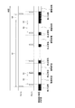
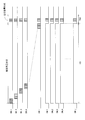
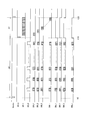
- FIG. 6 is a signal waveform diagram for describing generation of drive signals for drive lines in the first embodiment. It is a signal waveform diagram for demonstrating the drive method of the electrode group for position detection in the modification of the said 1st Embodiment. It is a block diagram which shows the detailed structure of the detection apparatus which concerns on the 2nd Embodiment of this invention.
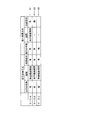
- the said 3rd Embodiment it is a figure for demonstrating the electrode group drive system prepared for the detection apparatus by the 3rd specific example.
- FIG. 2 is a block diagram showing an overall configuration of the electronic apparatus 1 including the detection device 10 according to the first embodiment of the present invention.
- the electronic device 1 is constituted by a detection device 10 and a liquid crystal display device 20.
- the electronic apparatus 1 may further include a controller that mediates exchange of various data between the detection device 10 and the liquid crystal display device 20.
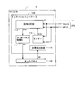
- the detection device 10 is configured by a touch panel controller 100 and a touch panel 120.
- a detection control unit is realized by the touch panel controller 100
- a sensing unit is realized by the touch panel 120.
- the touch panel controller 100 receives the synchronization signal group SYG sent from the display controller 200 in the liquid crystal display device 20 and outputs a drive signal SD for performing position detection processing to the touch panel 120.
- a series of processes for detecting a position where an object to be detected (detection object) contacts or approaches the touch panel 120 is referred to as a “position detection process”.
- the touch panel 120 detects contact or approach of an object to be detected such as a finger of a user (operator of the electronic device 1) or a touch pen.
- the detection timing is determined based on the drive signal SD output from the touch panel controller 100.
- the detection result is sent from the touch panel 120 to the touch panel controller 100 as a sense signal SX.
- a control signal CTL is sent from the touch panel controller 100 to the display controller 200 according to the position.
- the liquid crystal display device 20 includes a display controller 200, a source driver (video signal line driving circuit) 210, a gate driver (scanning signal line driving circuit) 220, a common electrode driver 230, and a liquid crystal panel 240.
- the liquid crystal panel 240 includes a display unit 242 that displays an image. Note that a configuration (monolithic configuration) in which at least one of the source driver 210, the gate driver 220, and the common electrode driver 230 is provided in the liquid crystal panel 240 may be employed.
- the display unit 242 includes a plurality (n) of source bus lines (video signal lines) SL1 to SLn and a plurality (m) of gate bus lines (scanning signal lines) GL1 to GLm. It is installed.
- a pixel forming portion 3 for forming pixels is provided corresponding to each intersection of the source bus lines SL1 to SLn and the gate bus lines GL1 to GLm. That is, the display unit 242 includes a plurality (n ⁇ m) of pixel forming units 3.
- the plurality of pixel forming portions 3 are arranged in a matrix to form a pixel matrix of m rows ⁇ n columns.
- Each pixel forming unit 3 includes a TFT 30 which is a switching element having a gate terminal connected to a gate bus line GL passing through a corresponding intersection and a source terminal connected to a source bus line SL passing through the intersection.
- the pixel electrode 31 is connected to the drain terminal of the TFT 30, the common electrode 34 and the auxiliary capacitance electrode 35 provided in common to the plurality of pixel forming portions 3, and the pixel electrode 31 and the common electrode 34.
- a liquid crystal capacitor 32 and an auxiliary capacitor 33 formed by the pixel electrode 31 and the auxiliary capacitor electrode 35 are included.
- the liquid crystal capacitor 32 and the auxiliary capacitor 33 constitute a pixel capacitor 36.
- an oxide TFT (a thin film transistor using an oxide semiconductor for a channel layer) can be employed. More specifically, In—Ga—Zn—O (indium gallium zinc oxide) which is an oxide semiconductor mainly containing indium (In), gallium (Ga), zinc (Zn), and oxygen (O) is used.
- In—Ga—Zn—O—TFT indium gallium zinc oxide
- a TFT in which a channel layer is formed hereinafter referred to as “In—Ga—Zn—O—TFT”
- In—Ga—Zn—O—TFT an In—Ga—Zn—O—TFT
- a transistor in which an oxide semiconductor other than In—Ga—Zn—O (indium gallium zinc oxide) is used for a channel layer can be employed.
- an oxide semiconductor other than In—Ga—Zn—O indium gallium zinc oxide
- at least one of indium, gallium, zinc, copper (Cu), silicon (Si), tin (Sn), aluminum (Al), calcium (Ca), germanium (Ge), and lead (Pb) is included.
- the present invention does not exclude the use of TFTs other than oxide TFTs.
- the display controller 200 receives the control signal CTL from the touch panel controller 100. Further, the display controller 200 outputs a digital video signal DV, a source start pulse signal SSP, a source clock signal SCK, and a latch strobe signal LS to the source driver 210, and a gate start pulse signal GSP and a gate driver 220.
- the gate clock signal GCK is output
- the common electrode drive signal SVC is output to the common electrode driver 230
- the synchronization signal group SYG is output to the touch panel controller 100.
- the source driver 210 receives the digital video signal DV, the source start pulse signal SSP, the source clock signal SCK, and the latch strobe signal LS sent from the display controller 200, and applies a driving video signal to each source bus line SL. At this time, the source driver 210 sequentially holds the digital video signal DV indicating the voltage to be applied to each source bus line SL at the timing when the pulse of the source clock signal SCK is generated. The held digital video signal DV is converted into an analog voltage at the timing when the pulse of the latch strobe signal LS is generated. The converted analog voltage is applied simultaneously to all the source bus lines SL1 to SLn as drive video signals.
- the gate driver 220 Based on the gate start pulse signal GSP and the gate clock signal GCK sent from the display controller 200, the gate driver 220 repeats the application of the active scanning signal to each gate bus line GL with a period of one vertical scanning period.
- the common electrode driver 230 applies a predetermined voltage Vcom to the common electrode 34 based on the common electrode drive signal SVC sent from the display controller 200.
- the driving video signal is applied to the source bus lines SL1 to SLn
- the scanning signal is applied to the gate bus lines GL1 to GLm
- the predetermined voltage Vcom is applied to the common electrode 34, thereby displaying the display.
- An image is displayed in the part 242.
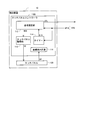
- FIG. 3 is a block diagram showing a detailed configuration of the detection apparatus 10 in the present embodiment.
- the detection device 10 includes the touch panel controller 100 and the touch panel 120.
- the touch panel controller 100 includes a touch panel drive unit 110, a signal selection unit 112, a timer 114, and a coordinate detection circuit 116.
- the touch panel 120 has a plurality of electrodes (hereinafter referred to as “position detection electrode group”) for position detection formed in an area corresponding to the display unit 242 of the liquid crystal display device 20.
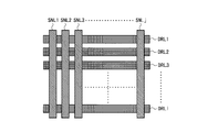
- FIG. 4 is a schematic diagram showing the configuration of the position detection electrode group.
- i drive lines DRL1 to DRLi and j sense lines SNL1 to SNLj are arranged in the touch panel 120 as position detection electrode groups so as to intersect each other.
- the touch panel controller 100 receives a synchronization signal group SYG sent from the display controller 200 in the liquid crystal display device 20.
- the synchronization signal group SYG includes a vertical synchronization signal Vsync and a general-purpose input / output signal GPIO.
- the general-purpose input / output signal GPIO is a signal that is intentionally output from the display controller 200.
- the timer 114 includes a clock generator (not shown) that generates an internal clock, a counter (not shown) that counts the internal clock, and the like.
- the timer 114 generates an internal signal group SIG based on the synchronization signal group SYG, and outputs the internal signal group SIG to the signal selection unit 112.
- the signal selection unit 112 receives the synchronization signal group SYG and the internal signal group SIG.
- the signal selection unit 112 selects one or more signals from the input signals.
- the signal selected by the signal selection unit 112 is given to the touch panel drive unit 110 as a selection signal group SEG.
- the touch panel driving unit 110 receives a driving signal SD for driving the position detection electrode groups (driving lines DRL1 to DRLi and sensing lines SNL1 to SNLj) as a touch panel. 120 for output.
- the touch panel 120 detects contact or approach of an object to be detected at a timing based on the drive signal SD.
- the coordinate detection circuit 116 calculates coordinates for specifying the position (position on the touch panel 120) where the detected object comes into contact or approaches based on the sense signal SX as the detection result. Based on the coordinates calculated by the coordinate detection circuit 116, for example, a menu selected by the user from among a plurality of menus displayed on the display unit 242 is specified.
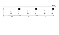
- the liquid crystal display device 20 repeats vertical scanning (see FIG. 5).
- the vertical scanning period which is a period in which one vertical scanning is performed, includes an effective vertical scanning period 51 and a vertical blanking period 52.
- one vertical scanning period is represented by “1V”.
- the liquid crystal display device 20 horizontal scanning is repeated in each vertical scanning period (see FIG. 6).
- the horizontal scanning period in which one horizontal scanning is performed includes an effective horizontal scanning period 53 and a horizontal blanking period 54.
- one horizontal scanning period is represented by “1H”.
- the falling point of the vertical synchronizing signal Vsync is the starting point of the vertical scanning period
- the falling point of the horizontal synchronizing signal Hsync is the horizontal scanning period. It is the start time.
- the liquid crystal display device 20 is in a driving state during the effective horizontal scanning period 53 (period other than the horizontal blanking period 54 of the effective vertical scanning period 51), and the vertical blanking period 52 and horizontal In the blanking period 54, the liquid crystal display device 20 is in a resting state.
- the vertical blanking period 52 and the horizontal blanking period 54 are pause periods.
- FIG. 8 is a waveform diagram showing a state of noise N generated from a certain liquid crystal display device. 8 that the noise N level in the horizontal blanking period 54 is considerably smaller than the noise N level in the effective horizontal scanning period 53. As described above, during the period in which the driving of the liquid crystal display device is stopped (the period in which the writing signal is not output to the display unit 242), the level of noise generated from the liquid crystal display device is small. It is preferable that position detection processing for realizing a function that is easily affected by noise is performed in such a period where the noise level is low, that is, a pause period.
- a general driving method of the position detection electrode group when the position detection process is performed will be described with reference to FIG.
- the drive lines DRL1 to DRLi are driven one by one with all the sensing lines SNL1 to SNLj being turned on.
- the position detection process is performed by the self-capacitance method
- all the drive lines DRL1 to DRLi and all the sense lines SNL1 to SNLj are driven at the same time.
- the drive lines DRL1 to DRLi and the sense lines SNL1 to SNLj are driven in this way.
- a vertically striped waveform (a waveform indicated by reference numeral 58 in FIG. 10) has a plurality of pulses (pulses) as indicated by reference numeral 59 in FIG. 10. The number is not particularly limited).
- the drive lines DRL1 to DRLi are driven line by line while all the sensing lines SNL1 to SNLj are turned on. Further, during the vertical blanking period 52, all the drive lines DRL1 to DRLi and all the sense lines SNL1 to SNLj are driven at the same time. Therefore, in the present embodiment, position detection processing by the mutual capacitance method is performed in the effective vertical scanning period 51, and position detection processing by the self-capacitance method is performed in the vertical blanking period 52. Note that the position detection processing by the mutual capacitance method is performed in the horizontal blanking period 54 in the effective vertical scanning period 51 as described in detail later.
- the vertical synchronization signal Vsync is used to perform position detection processing by the mutual capacitance method in the effective vertical scanning period 51 (specifically, the horizontal blanking period 54 in the effective vertical scanning period 51).
- the general-purpose input / output signal GPIO is used.
- the vertical synchronization signal Vsync falls at time t0.
- This time t0 is the start time of the effective vertical scanning period 51.
- the drive lines DRL1 to DRLi are driven line by line. Further, all the sensing lines SNL1 to SNLj are maintained in the ON state throughout the effective vertical scanning period 51.
- drive signals for the drive lines DRL1 to DRLi and drive signals for the sense lines SNL1 to SNLj are generated, for example, as follows.
- the timer 114 (see FIG. 3) generates the mutual capacitance synchronization selection signal SEL1 by counting the internal clock based on the falling edge of the vertical synchronization signal Vsync (see FIGS. 1 and 11).
- the timer 114 counts the internal clock based on the falling edge of the vertical synchronization signal Vsync, so that the first row driving synchronization signal SYN-DR1, the second row driving synchronization signal SYN-DR2,.
- a row driving synchronization signal SYN-DRi (not shown) is generated.
- the mutual capacitance synchronization selection signal SEL1 is output at a time point t1 after a lapse of a period corresponding to a predetermined number of internal clocks from a time point t0 when the vertical synchronization signal Vsync falls.
- the pulse of the pulse and the first row driving synchronization signal SYN-DR1 rises.
- the mutual capacitance synchronization selection signal SEL1 pulses are generated at predetermined intervals throughout the effective vertical scanning period 51.
- the pulse of the second row driving synchronization signal SYN-DR2 rises.
- the second-row driving synchronization signal SYN-DR2 For the second-row driving synchronization signal SYN-DR2, four pulses are generated during the period from the time point t2 to the time point t3. In this manner, the first row driving synchronization signal SYN-DR1 to the i-th row driving synchronization signal SYN-DRi are each pulsed four times during the effective vertical scanning period 51.
- the mutual capacitance synchronization selection signal SEL1 and the first row driving synchronization signal SYN-DR1 to the i-th row driving synchronization signal SYN-DRi generated by the timer 114 as described above are signals included in the internal signal group SIG.
- the signal selection unit 112 is provided.
- the signal selection unit 112 uses the mutual capacitance synchronization selection signal SEL1 and the first row driving synchronization signal SYN-DR1 to i-th row driving synchronization signal SYN-DRi as signals included in the selection signal group SEG.
- the touch panel drive unit 110 generates a drive signal for the drive line DRL1 based on the mutual capacitance synchronization selection signal SEL1 and the first row drive synchronization signal SYN-DR1.
- the drive signal for the drive line DRL1 becomes a high level when both the mutual capacitance synchronization selection signal SEL1 and the first row drive synchronization signal SYN-DR1 are at a high level.
- the touch panel driving unit 110 drives the drive lines DRL2 to DRLi based on the mutual capacitance synchronization selection signal SEL1 and the second row driving synchronization signal SYN-DR2 to the i-th row driving synchronization signal SYN-DRi.
- a driving signal is generated.
- the touch panel driving unit 110 generates driving signals for the sensing lines SNL1 to SNLj based on the mutual capacitance synchronization selection signal SEL1.
- the drive signals for the sensing lines SNL1 to SNLj are maintained at a high level throughout the effective vertical scanning period 51.
- the general-purpose input / output signal GPIO falls.
- This time t10 is the start time of the vertical blanking period 52.
- the self-capacitance synchronization selection signal SEL ⁇ b> 2 is maintained in an on state during a predetermined period in the vertical blanking period 52.
- all the drive lines DRL1 to DRLi and all the sense lines SNL1 to SNLj are driven at the same time.
- the drive signals for the drive lines DRL1 to DRLi and the drive signals for the sense lines SNL1 to SNLj are generated as follows, for example.
- the timer 114 generates the self-capacitance synchronization selection signal SEL2 by counting the internal clock based on the falling edge of the general-purpose input / output signal GPIO.
- the self-capacitance synchronization selection signal SEL2 is a signal that becomes a high level only for a predetermined period in the vertical blanking period 52.
- the self-capacitance synchronization selection signal SEL2 generated by the timer 114 is given to the signal selection unit 112 as a signal included in the internal signal group SIG.
- the signal selection unit 112 gives the self-capacitance synchronization selection signal SEL2 to the touch panel drive unit 110 as a signal included in the selection signal group SEG.
- the touch panel drive unit 110 generates drive signals for the drive lines DRL1 to DRLi and drive signals for the sense lines SNL1 to SNLj based on the self-capacitance synchronization selection signal SEL2. More specifically, the touch panel driver 110 maintains the drive signals for the drive lines DRL1 to DRLi and the drive signals for the sense lines SNL1 to SNLj at the high level during the period when the self-capacitance synchronization selection signal SEL2 is at the high level. To do.
- the drive lines DRL1 to DRLi are sequentially driven using the horizontal blanking period 54 while all the sensing lines SNL1 to SNLj are maintained in the ON state.
- the vertical blanking period 52 all the drive lines DRL1 to DRLi and all the sense lines SNL1 to SNLj are driven at the same time.
- the control method of the detection apparatus 10 includes a self-drive that drives the position detection electrode group so that position detection processing is performed in a self-capacitance manner.
- a capacitance method detection step and a mutual capacitance method detection step for driving the position detection electrode group so that position detection processing is performed by the mutual capacitance method are included.
- the position detection electrode group is driven based on the synchronization signal in both the self-capacitance detection step and the mutual capacitance detection step.
- the configuration of the touch panel controller 100 the configuration of the synchronization signal SYG used for position detection processing, the generation method of the drive signals (the drive signals for the drive lines DRL1 to DRLi and the drive signals for the sense lines SNL1 to SNLj) SD, etc. Is not limited to those described above.
- the position detection electrode group when position detection processing by the mutual capacitance method is performed, the position detection electrode group is driven based on the vertical synchronization signal Vsync, and when position detection processing by the self-capacitance method is performed.
- the position detection electrode group is driven based on the general-purpose input / output signal GPIO.
- position detection processing by the mutual capacitance method is performed in the horizontal blanking period 54 in the effective vertical scanning period 51, and position detection processing by the self capacitance method is performed in the vertical blanking period 52.
- the position detection process using a relatively short pause period is performed, and the position detection process using a relatively long pause period is performed.
- the function which the user of the electronic device 1 uses it becomes possible to use properly the result of the position detection process performed in two types of idle periods.
- the performance of the touch panel 120 can be improved by properly using the results of the position detection processing performed in two types of pause periods. Can be fully exhibited.
- the detection device 10 that can sufficiently exhibit performance even when used integrally with a high-resolution liquid crystal display device (a liquid crystal display device having a relatively short pause period). Realized.
- the position detection process by the mutual capacitance method is performed in the horizontal blanking period 54 in the effective vertical scanning period 51 and the position detection process by the self-capacitance method is performed in the vertical blanking period 52. It was. However, the present invention is not limited to this. As in this modification, position detection processing by the self-capacitance method is performed in the horizontal blanking period 54 in the effective vertical scanning period 51, and position detection processing by the mutual capacitance method is performed in the vertical blanking period 52. Also good.
- FIG. 12 is a signal waveform diagram for explaining a driving method of the position detection electrode group in this modification.
- a pulse of the self-capacitance synchronization selection signal SEL2 is generated after a lapse of a predetermined period from the time t0 when the vertical synchronization signal Vsync falls.
- the pulses of the self-capacitance synchronization selection signal SEL2 are generated at predetermined intervals throughout the effective vertical scanning period 51.
- the self-capacitance synchronization selection signal SEL2 is generated so that this pulse occurs in the horizontal blanking period 54.
- the general-purpose input / output signal GPIO falls at time t10. Based on the general-purpose input / output signal GPIO, all the sensing lines SNL1 to SNLj are maintained in the ON state throughout the vertical blanking period 52.
- the vertical blanking period 52 as in the effective vertical scanning period 51 in the first embodiment, the mutual capacitance synchronization selection signal SEL1 and the first row driving synchronization signal SYN-DR1.
- the i-th row driving synchronization signal SYN-DRi is generated, and the driving signals for the driving lines DRL1 to DRLi are generated based on these signals.
- the drive lines DRL1 to DRLi are driven line by line in the vertical blanking period 52.
- the position detection process is performed using two types of pause periods. Therefore, as in the first embodiment, even if the liquid crystal display device 20 that is used integrally with the detection device 10 is a high-resolution display device, the result of the position detection processing performed in two types of pause periods. By properly using these, the performance of the touch panel 120 can be fully exhibited.
- Second Embodiment> A second embodiment of the present invention will be described. Only differences from the first embodiment will be described.
- FIG. 13 is a block diagram showing a detailed configuration of the detection apparatus 10 in the present embodiment.
- the vertical synchronization signal Vsync and the general-purpose input / output signal GPIO are input to the touch panel controller 100 as the synchronization signal SYG.
- the general-purpose input / output signal GPIO is input to the touch panel controller 100 as the synchronization signal SYG.
- Other points are the same as in the first embodiment.
- FIG. 14 is a signal waveform diagram for explaining a driving method of the position detection electrode group in the present embodiment.
- all drive lines DRL1 to DRLi and all sense lines SNL1 to SNLj are driven simultaneously.
- the drive lines DRL1 to DRLi are driven one by one with all the sensing lines SNL1 to SNLj being turned on. Therefore, in the present embodiment, position detection processing by the self-capacitance method is performed in the vertical blanking period 52, and position detection processing by the mutual capacitance method is performed in a period other than the vertical blanking period 52. This will be described in detail below.
- the general-purpose input / output signal GPIO is used to perform position detection processing by the self-capacitance method in the vertical blanking period 52.
- the synchronization signal is not used for the position detection process using the mutual capacitance method. That is, in the present embodiment, the position detection process by the mutual capacitance method is performed asynchronously with the driving operation of the liquid crystal display device 20.
- the drive line DRL1 in order to perform the position detection process by the mutual capacitance method, the drive line DRL1 is turned on in a state where all the sensing lines SNL1 to SNLj are turned on at a predetermined cycle without being based on the synchronization signal.
- ⁇ DRLi is driven line by line.
- the touch panel controller 100 is controlled to stop such driving operation.
- the drive lines DRL1 to DRLi are driven line by line while all the sensing lines SNL1 to SNLj are turned on.
- the general-purpose input / output signal GPIO falls at time t10.
- This time t10 is the start time of the vertical blanking period 52.
- the self-capacitance synchronization selection signal SEL2 is maintained in the ON state during a predetermined period in the vertical blanking period 52.
- all the drive lines DRL1 to DRLi and all the sense lines SNL1 to SNLj are driven at the same time.
- the drive lines DRL1 to DRLi and the sense lines SNL1 to SNLj are driven in the same manner as in the first embodiment (see FIG. 1).
- the position detection process by the self-capacitance method is performed in the vertical blanking period 52 in synchronization with the driving operation of the liquid crystal display device 20, and the position detection process by the mutual capacitance method is performed by the liquid crystal display. It is performed in a period other than the vertical blanking period 52 without synchronizing with the driving operation of the apparatus 20.
- the position detection process by the self-capacitance method is performed in the horizontal blanking period 54 in synchronization with the drive operation of the liquid crystal display device 20, and the position detection process by the mutual capacitance method is synchronized with the drive operation of the liquid crystal display device 20. Alternatively, it may be performed in a period other than the horizontal blanking period 54.
- the position detection electrode group is driven based on the general-purpose input / output signal GPIO.
- the position detection electrode group is driven based on the synchronization signal in this way, it is possible to perform position detection processing by the self-capacitance method during the pause period of the liquid crystal display device 20.
- the position detection process by the mutual capacitance method is performed asynchronously with the driving operation of the liquid crystal display device 20.
- the position detection process is performed during the pause period of the liquid crystal display device 20 and the position detection process is also performed during the drive period of the liquid crystal display device 20.
- a position detection process for realizing a function having a large influence of noise is performed during a pause period of the liquid crystal display device 20
- a position detection process for realizing a function having a small influence of noise is performed by driving the liquid crystal display device 20.
- the performance of the touch panel 120 can be sufficiently exhibited.
- the detection device 10 that can sufficiently exhibit performance even when used integrally with a high-resolution liquid crystal display device (a liquid crystal display device having a relatively short pause period). Realized.
- the position detection process by the self-capacitance method is performed in the vertical blanking period 52 and the position detection process by the mutual capacitance method is performed in a period other than the vertical blanking period 52.
- the present invention is not limited to this.
- position detection processing by the mutual capacitance method may be performed in the vertical blanking period 52 and position detection processing by the self-capacitance method may be performed in a period other than the vertical blanking period 52.
- FIG. 15 is a signal waveform diagram for explaining a driving method of the position detection electrode group in the present modification.
- the present modification in order to perform the position detection process by the self-capacitance method, all the drive lines DRL1 to DRLi and all the sense lines SNL1 to SNLj are simultaneously transmitted at a predetermined cycle without using the synchronization signal. Driven. However, in the vertical blanking period 52, the touch panel controller 100 is controlled to stop such driving operation. As described above, as shown in FIG. 15, in the period other than the vertical blanking period 52, all the drive lines DRL1 to DRLi and all the sense lines SNL1 to SNLj are driven simultaneously.
- the general-purpose input / output signal GPIO falls at time t10. Based on the general-purpose input / output signal GPIO, all the sensing lines SNL1 to SNLj are maintained in the ON state throughout the vertical blanking period 52.
- the vertical blanking period 52 as in the effective vertical scanning period 51 in the first embodiment, the mutual capacitance synchronization selection signal SEL1 and the first row driving synchronization signal SYN-DR1.
- the i-th row driving synchronization signal SYN-DRi is generated, and the driving signals for the driving lines DRL1 to DRLi are generated based on these signals.
- the drive lines DRL1 to DRLi are driven line by line in the vertical blanking period 52.
- the position detection process is performed during the pause period of the liquid crystal display device 20 and the position detection process is also performed during the drive period of the liquid crystal display device 20. Therefore, as in the second embodiment, even if the liquid crystal display device 20 used integrally with the detection device 10 is a high-resolution display device, the result and driving of the position detection process performed during the pause period. By properly using the result of the position detection process performed during the period according to the function, the performance of the touch panel 120 can be sufficiently exhibited.
- FIG. 16 is a block diagram showing a detailed configuration of the detection apparatus 10 in the present embodiment.
- the touch panel controller 100 is provided with a drive switching unit 118 in addition to the components (see FIG. 3) in the first embodiment.
- the vertical synchronization signal Vsync, the horizontal synchronization signal Hsync, and the general-purpose input / output signal GPIO are input to the touch panel controller 100 as the synchronization signal group SYG.
- the drive switching unit 118 detects a predetermined item (hereinafter referred to as “switching factor item”) Msw, the drive switching unit 118 selects a switching signal SWa, SWb, and SWc as a timer 114 and a signal selection, respectively, in order to switch an electrode group driving method to be described later.
- switching factor item a predetermined item
- the switching factor Msw include selection of a predetermined menu (function) by the user, putting in and out of the touch pen with respect to the electronic device 1, attachment of water droplets on the touch panel 120, and the like.
- position detection processing by the self-capacitance method is performed in the vertical blanking period 52, and position detection processing by the mutual capacitance method is performed in the horizontal blanking period 54 (see FIG. 1).
- This case is referred to as “case A” for convenience.
- position detection processing by the self-capacitance method is performed in the vertical blanking period 52, and the period is not synchronized with the driving operation of the liquid crystal display device 20 in a period other than the vertical blanking period 52.
- Position detection processing by a capacity method has been performed (see FIG. 14) (this case is referred to as “case B” for convenience).
- electrode group driving method is used to indicate how the position detection process is executed in each case described above. More specifically, whether or not position detection processing is performed in the self-capacitance method, whether or not position detection processing is performed in the mutual capacitance method, and the position detection processing when the position detection processing is performed in the self-capacitance method.
- a method of driving the position detection electrode group by the touch panel controller 100 is referred to as an “electrode group driving method”.
- the electrode group driving method in the case A described above is specified as a row indicated by an arrow 61 in FIG. 17, and the electrode group driving method in the case B described above is a row indicated by an arrow 62 in FIG.
- the electrode group driving method in the case C described above is specified as shown by a row indicated by an arrow 63 in FIG.
- the detection device 10 is configured such that the above-described electrode group driving method can be switched during the operation of the electronic device 1. That is, in the present embodiment, the position detection processing may be switched from the execution in the first embodiment to the execution in the second embodiment, for example. Specifically, the switching of the electrode group driving method is performed when the drive switching unit 118 detects the switching factor Msw as described above. The drive switching unit 118 outputs the switching signals SWa, SWb, and SWc according to the contents of the switching factor Msw, so that the timer 114, the signal selection unit 112, and the touch panel driving unit 110 have a desired electrode group driving method. Various signals (internal signal group SIG, selection signal group SEG, drive signal SD) are generated so that the position detection electrode group is driven.
- the position detection processing by the self-capacitance method or the mutual capacitance method does not have to be performed based on the synchronization signal in all the electrode group driving methods prepared in the detection apparatus 10.
- the position detection processing by the self-capacitance method is not performed, and the position detection processing by the mutual capacitance method is performed without being based on the synchronization signal.
- the position detection process by the mutual capacitance method is performed in the vertical blanking period 52 based on the synchronization signal.
- the synchronization signal is generated when the position detection process is performed by at least one of the self-capacitance method and the mutual capacitance method.
- the position detection electrode group may be driven based on the above.
- two functions “function F2” and “function F3” can be selected by the user, and three electrode group driving methods “method M1,” “method M2,” and “method M3” are detected.
- the device 10 is provided.
- a suitable electrode group driving method for realizing the function F2 is the method M2
- a suitable electrode group driving method for realizing the function F3 is the method M3.
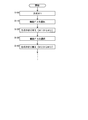
- FIG. 19 is a flowchart for explaining a first example relating to the flow of switching of the electrode group driving method.
- the electrode group driving method is set to the method M1 (step S100).
- the electrode group driving method is switched from the method M1 to the method M2 (step S120).
- the function F3 is selected by the user (step S130)
- the electrode group driving method is switched from the method M2 to the method M3 (step S140).
- every time a function is selected by the user switching to the electrode group driving method suitable for executing the selected function is performed.
- the electrode group driving method suitable for executing them is the same. In such a case, even if the function to be executed is switched between these two functions, the electrode group driving method is not switched.
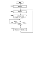
- FIG. 20 is a flowchart for explaining a second example regarding the flow of switching of the electrode group driving method.
- the electrode group driving method is set to the method M1 (step S200).
- the electrode group driving method is switched from the method M1 to the method M2 (step S220).
- the electrode group driving method is switched from the method M2 to the method M1 (step S240).
- the electrode group driving method is switched from the method M1 to the method M3 (step S260).
- the electrode group driving method is switched from the method M3 to the method M1 (step S280).
- the position detection processing is usually performed based on the initially set electrode group driving method, and the electrode group driving suitable for the execution of the function is performed only during the period during which the predetermined function is being executed. Switch to the method.
- the electrode group driving method switching step is realized by steps S120 and S140.
- the electrode group driving method switching step is realized by step S220, step S240, step S260, and step S280.
- the flow of switching the electrode group driving method is not limited to the flow shown in the above two examples.
- the matter (switching factor matter Msw) that causes the switching of the electrode group driving method is not limited to the selection of the function by the user.
- the electrode group driving method is switched by, for example, putting in and out the touch pen with respect to the electronic device 1 and attaching water droplets to the touch panel 120.
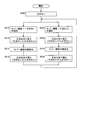
- FIG. 22 is a flowchart for explaining a first specific example regarding the flow of switching of the electrode group driving method.
- the electrode group driving method is set to the method Ma (step S400).
- the touch pen is inserted into a predetermined position of the electronic device 1.
- the electronic device 1 as a case where the pen input function is started, a case where the user intentionally switches to the pen mode by executing a predetermined application, and a touch pen is a terminal There is a case where switching to the pen mode is performed without the user's intention by being extracted from the (electronic device 1).
- step S410 When the user intentionally switches to the pen mode (step S410), the electrode group driving method is switched from the method Ma to the method Mb (step S412). Thereafter, when the pen input function is invalidated by terminating the application (step S414), the electrode group driving method is switched from the method Mb to the method Ma (step S416). After the completion of step S416, the state returns to the state immediately after step S400.
- step S420 When the touch pen is removed from the terminal (step S420), the electrode group driving method is switched from the method Ma to the method Mb (step S422). Thereafter, when the touch pen is housed in the terminal (step S424), the electrode group driving method is switched from the method Mb to the method Ma (step S426). After the end of step S426, the process returns to the state immediately after step S400.
- the position detection process by the mutual capacitance method is not performed during the period when the pen input function is executed, and the position by the self-capacitance method is used.
- the position detection electrode group is driven so that the detection process is performed in the vertical blanking period 52.
- Position detection is performed so that the position detection process by the self-capacitance method is not performed during the period other than the period when the pen input function is executed and the position detection process by the mutual capacitance method is performed in the vertical blanking period 52.
- the electrode group for driving is driven. In this way, the electrode group driving method is switched.
- the position detection processing by the self-capacitance method is performed in the vertical blanking period 52 using the synchronization signal, and the position detection processing by the mutual capacitance method is performed by using the synchronization signal.
- the electrode group driving method is switched at the start / end timing of the execution of the hover function (function capable of operating the terminal without directly touching the panel).
- FIG. 24 is a flowchart for explaining a second specific example regarding the flow of switching of the electrode group driving method.
- the electrode group driving method is set to the method Mc (step S500).
- the hover function is not executed.
- a mode when the hover function is executed a first mode that allows an instruction of only one point and a second mode that allows an instruction of two or more points And are prepared.
- step S510 When the user instructs the start of execution of the hover function in the first mode (step S510), the electrode group driving method is switched from the method Mc to the method Md (step S512). Thereafter, when the hover function is invalidated by terminating the application (step S514), the electrode group driving method is switched from the method Md to the method Mc (step S516). After step S516 is completed, the process returns to the state immediately after step S500.
- step S520 when the user instructs the start of execution of the hover function in the second mode (step S520), the electrode group driving method is switched from the method Mc to the method Me (step S522). Thereafter, when the hover function is invalidated by ending the application (step S524), the electrode group driving method is switched from the method Me to the method Mc (step S526). After step S526 is completed, the process returns to the state immediately after step S500.
- the position detection processing by the mutual capacitance method is not performed during the period when the hover function according to the first mode is executed, and the self-capacitance is performed.
- the position detection electrode group is driven so that the position detection process by the method is performed in the vertical blanking period 52.
- position detection processing by the self-capacitance method is performed in the vertical blanking period 52, and position detection processing by the mutual capacitance method is performed in the horizontal blanking period 54.
- the position detection electrode group is driven.
- the position detection electrode group is not performed so that the position detection process by the self-capacitance method is performed and the position detection process by the mutual capacitance method is performed in the horizontal blanking period 54. Is driven. In this way, the electrode group driving method is switched.
- FIG. 26 is a flowchart for explaining a third specific example regarding the flow of switching of the electrode group drive system.
- the electrode group driving method is set to the method Mf (step S600).
- whether or not water droplets are attached to the touch panel 120 is automatically determined by an IC configuring the detection apparatus 10 regardless of the operation by the user.
- step S610 When the adhesion of water droplets to the touch panel 120 is detected (step S610), the electrode group driving method is switched from the method Mf to the method Mg (step S620). Thereafter, it is sequentially determined whether or not water droplets are attached (step S630). When the adhesion of water droplets to the touch panel 120 is no longer detected, the electrode group driving method is switched from the method Mg to the method Mf (step S640). After step S640 is completed, the process returns to the state immediately after step S600.
- the position detection process by the self-capacitance method is performed in the vertical blanking period 52 during the period in which the water droplets are attached to the touch panel 120, and The position detection electrode group is driven so that the position detection process by the mutual capacitance method is performed in the horizontal blanking period 54. While the water droplets are not attached to the touch panel 120, the position detection process by the self-capacitance method is not performed, and the position detection process by the mutual capacitance method is performed in the horizontal blanking period 54.
- the electrode group is driven. In this way, the electrode group driving method is switched.
- the electrode group driving method (how the position detection process is executed) is switched in accordance with a predetermined switching factor Msw. Further, in any one of the plurality of electrode group driving methods prepared in the detection apparatus 10, position detection processing by at least one of the self-capacitance method and the mutual capacitance method is performed based on the synchronization signal. Therefore, by adopting a configuration in which the electrode group driving method is appropriately switched according to the magnitude of the influence of noise on the function to be executed, the rest period of the liquid crystal display device 20 can be used efficiently without causing malfunction.
- Various functions provided in the detection apparatus 10 can be realized. As described above, a detection device that can sufficiently exhibit performance even when used integrally with a high-resolution display device (a display device with a relatively short pause period) is realized.
- the present invention is not limited to the above embodiments and the above modifications, and various modifications can be made without departing from the scope of the present invention.
- the present invention can be applied to a case where the display device used in an integrated manner with the detection device 10 is a display device other than a liquid crystal display device such as an organic EL (Electro Luminescence) display device.
- Sensing line Hsync Horizontal sync signal Vsync ... Vertical sync signal GPIO ... General-purpose input / output signal SEL1 ... Mutual capacitance sync selection signal SEL2 ... Self-capacitance synchronization selection signal SYG ... Synchronization signal group
Landscapes
- Engineering & Computer Science (AREA)
- General Engineering & Computer Science (AREA)
- Theoretical Computer Science (AREA)
- Human Computer Interaction (AREA)
- Physics & Mathematics (AREA)
- General Physics & Mathematics (AREA)
- Position Input By Displaying (AREA)
- Control Of Indicators Other Than Cathode Ray Tubes (AREA)
- Liquid Crystal Display Device Control (AREA)
Abstract
Description
前記位置検出処理による位置の検出が行われるべき領域に形成された位置検出用電極群を有する感知部と、
前記位置検出処理を行うために前記位置検出用電極群を駆動する検出制御部と
を備え、
前記検出制御部は、自己容量方式および相互容量方式のうちの少なくとも一方の方式で前記位置検出処理が行われる際、同期信号に基づいて前記位置検出用電極群を駆動することを特徴とする。
外部の表示装置の画像表示部に対応する領域に前記位置検出用電極群が形成され、
前記表示装置と一体化して使用されることを特徴とする。
前記検出制御部は、自己容量方式での前記位置検出処理および相互容量方式での前記位置検出処理のいずれもが前記表示装置の動作が停止している期間である休止期間に行われるよう、前記位置検出用電極群を駆動することを特徴とする。
自己容量方式および相互容量方式のうちの一方を第1の方式と定義して他方を第2の方式と定義したとき、
前記検出制御部は、
前記表示装置の水平帰線期間には、前記第1の方式での前記位置検出処理が行われるよう前記同期信号に基づいて前記位置検出用電極群を駆動し、
前記表示装置の垂直帰線期間には、前記第2の方式での前記位置検出処理が行われるよう前記同期信号に基づいて前記位置検出用電極群を駆動することを特徴とする。
前記検出制御部は、自己容量方式での前記位置検出処理および相互容量方式での前記位置検出処理のうちの一方が前記表示装置の動作が停止している期間である休止期間に行われるよう、前記位置検出用電極群を駆動することを特徴とする。
自己容量方式および相互容量方式のうちの一方を第1の方式と定義して他方を第2の方式と定義したとき、
前記検出制御部は、
前記表示装置の水平帰線期間には、前記第1の方式での前記位置検出処理が行われるよう前記同期信号に基づいて前記位置検出用電極群を駆動し、
前記表示装置の水平帰線期間以外の期間には、前記第2の方式での前記位置検出処理が行われるよう前記位置検出用電極群を駆動することを特徴とする。
自己容量方式および相互容量方式のうちの一方を第1の方式と定義して他方を第2の方式と定義したとき、
前記検出制御部は、
前記表示装置の垂直帰線期間には、前記第1の方式での前記位置検出処理が行われるよう前記同期信号に基づいて前記位置検出用電極群を駆動し、
前記表示装置の垂直帰線期間以外の期間には、前記第2の方式での前記位置検出処理が行われるよう前記位置検出用電極群を駆動することを特徴とする。
前記検出制御部は、自己容量方式での前記位置検出処理の実行の有無と、相互容量方式での前記位置検出処理の実行の有無と、自己容量方式での前記位置検出処理が実行される場合における当該位置検出処理が行われる期間および同期信号の使用の有無と、相互容量方式での前記位置検出処理が実行される場合における当該位置検出処理が行われる期間および同期信号の使用の有無との組み合わせによって特定される方式であって前記位置検出用電極群を駆動する方式である電極群駆動方式を、前記表示装置の動作中に切り替えることができることを特徴とする。
前記検出制御部は、実行される機能に応じて、前記電極群駆動方式を切り替えることを特徴とする。
前記電極群駆動方式として、初期状態に対応する第1の駆動方式と、少なくとも1つの特定機能に対応する第2の駆動方式とが予め用意され、
前記検出制御部は、前記特定機能の実行開始の際に前記電極群駆動方式を前記第1の駆動方式から前記第2の駆動方式に切り替え、前記特定機能の実行終了の際に前記電極群駆動方式を前記第2の駆動方式から前記第1の駆動方式に切り替えることを特徴とする。
前記検出制御部は、前記電極群駆動方式に応じて、使用する同期信号を切り替えることを特徴とする。
前記位置検出用電極群は、前記画像表示部に対応する領域に形成され、
前記同期信号は、前記表示装置から前記検出制御部に与えられることを特徴とする。
自己容量方式で前記位置検出処理が行われるよう、前記位置検出処理による位置の検出が行われるべき領域に形成された位置検出用電極群を駆動する自己容量方式検出ステップと、
相互容量方式で前記位置検出処理が行われるよう、前記位置検出用電極群を駆動する相互容量方式検出ステップと
を含み、
前記自己容量方式検出ステップおよび前記相互容量方式検出ステップのうちの少なくとも一方のステップでは、同期信号に基づいて前記位置検出用電極群が駆動されることを特徴とする。
自己容量方式での前記位置検出処理の実行の有無と、相互容量方式での前記位置検出処理の実行の有無と、自己容量方式での前記位置検出処理が実行される場合における当該位置検出処理が行われる期間および同期信号の使用の有無と、相互容量方式での前記位置検出処理が実行される場合における当該位置検出処理が行われる期間および同期信号の使用の有無との組み合わせによって特定される方式であって前記位置検出用電極群を駆動する方式である電極群駆動方式を切り替える電極群駆動方式切り替えステップを更に含むことを特徴とする。
<1.1 全体構成および動作概要>
図2は、本発明の第1の実施形態に係る検出装置10を含む電子機器1の全体構成を示すブロック図である。この電子機器1は、検出装置10と液晶表示装置20とによって構成されている。なお、検出装置10と液晶表示装置20との間での各種データのやりとりを媒介するコントローラが更に電子機器1に含まれていても良い。
図3は、本実施形態における検出装置10の詳細な構成を示すブロック図である。上述したように、検出装置10は、タッチパネルコントローラ100とタッチパネル120とによって構成されている。タッチパネルコントローラ100は、図3に示すように、タッチパネル駆動部110,信号選択部112,タイマー114,および座標検出回路116によって構成されている。
以下、本実施形態における位置検出処理について詳しく説明する。
はじめに、期間に関する基本的な事項について説明する。この電子機器1の動作中、液晶表示装置20では垂直走査が繰り返される(図5参照)。図5に示すように、1回の垂直走査が行われる期間である垂直走査期間は、有効垂直走査期間51と垂直帰線期間52とからなる。なお、図5では、1垂直走査期間を「1V」で表している。また、液晶表示装置20では、各垂直走査期間には水平走査が繰り返される(図6参照)。図6に示すように、1回の水平走査が行われる期間である水平走査期間は、有効水平走査期間53と水平帰線期間54とからなる。なお、図6では、1水平走査期間を「1H」で表している。
次に、図1および図11を参照しつつ、本実施形態における位置検出用電極群の駆動方法について説明する。本実施形態においては、有効垂直走査期間51(詳しくは、有効垂直走査期間51内の水平帰線期間54)に相互容量方式による位置検出処理を行うために、垂直同期信号Vsyncが用いられる。また、垂直帰線期間52に自己容量方式による位置検出処理を行うために、汎用入出力信号GPIOが用いられる。
本実施形態によれば、相互容量方式による位置検出処理が行われる際には、垂直同期信号Vsyncに基づいて位置検出用電極群が駆動され、自己容量方式による位置検出処理が行われる際には、汎用入出力信号GPIOに基づいて位置検出用電極群が駆動される。このように同期信号に基づいて位置検出用電極群を駆動することによって、液晶表示装置20の休止期間中に位置検出処理を行うことが可能となる。また、有効垂直走査期間51内の水平帰線期間54に相互容量方式による位置検出処理が行われ、垂直帰線期間52に自己容量方式による位置検出処理が行われる。すなわち、比較的短い休止期間を利用した位置検出処理が行われるとともに、比較的長い休止期間を利用した位置検出処理が行われる。これにより、電子機器1のユーザーが使用する機能に応じて、2種類の休止期間に行われた位置検出処理の結果を使い分けることが可能となる。このため、検出装置10と一体的に使用される液晶表示装置20が高解像度の表示装置であっても、2種類の休止期間に行われた位置検出処理の結果を使い分けることによってタッチパネル120の性能を充分に発揮することが可能となる。以上のように、本実施形態によれば、高解像度の液晶表示装置(休止期間が比較的短い液晶表示装置)と一体的に使用されても性能を充分に発揮することのできる検出装置10が実現される。
上記第1の実施形態においては、有効垂直走査期間51内の水平帰線期間54に相互容量方式による位置検出処理が行われるとともに垂直帰線期間52に自己容量方式による位置検出処理が行われていた。しかしながら、本発明はこれに限定されない。本変形例のように、有効垂直走査期間51内の水平帰線期間54に自己容量方式による位置検出処理が行われるとともに垂直帰線期間52に相互容量方式による位置検出処理が行われるようにしても良い。
本発明の第2の実施形態について説明する。なお、上記第1の実施形態と異なる点についてのみ説明する。
全体構成については、上記第1の実施形態と同様である(図2参照)。図13は、本実施形態における検出装置10の詳細な構成を示すブロック図である。上記第1の実施形態においては、タッチパネルコントローラ100には同期信号SYGとして垂直同期信号Vsyncおよび汎用入出力信号GPIOが入力されていた。これに対して、本実施形態においては、タッチパネルコントローラ100には同期信号SYGとして汎用入出力信号GPIOのみが入力される。それ以外の点については、上記第1の実施形態と同様である。
図14は、本実施形態における位置検出用電極群の駆動方法について説明するための信号波形図である。本実施形態においては、垂直帰線期間52中に、全ての駆動ラインDRL1~DRLiおよび全ての感知ラインSNL1~SNLjが一斉に駆動される。また、垂直帰線期間52以外の期間に、全ての感知ラインSNL1~SNLjがオンにされた状態で駆動ラインDRL1~DRLiが1ラインずつ駆動される。従って、本実施形態においては、垂直帰線期間52に自己容量方式による位置検出処理が行われ、垂直帰線期間52以外の期間に相互容量方式による位置検出処理が行われる。以下、詳しく説明する。
本実施形態によれば、自己容量方式による位置検出処理が行われる際には、汎用入出力信号GPIOに基づいて位置検出用電極群が駆動される。このように同期信号に基づいて位置検出用電極群を駆動することによって、液晶表示装置20の休止期間中に自己容量方式による位置検出処理を行うことが可能となる。また、自己容量方式による位置検出処理が行われる期間以外の期間に、液晶表示装置20の駆動動作とは非同期で相互容量方式による位置検出処理が行われる。すなわち、液晶表示装置20の休止期間中に位置検出処理が行われるとともに、液晶表示装置20の駆動期間中にも位置検出処理が行われる。ここで、ノイズの影響の大きい機能を実現するための位置検出処理を液晶表示装置20の休止期間中に行い、ノイズの影響の小さい機能を実現するための位置検出処理を液晶表示装置20の駆動期間中に行うことによって、誤動作を生ずることなく、検出装置10に設けられた各種機能が実現される。このようにして、検出装置10と一体的に使用される液晶表示装置20が高解像度の表示装置であっても、休止期間中に行われた位置検出処理の結果と駆動期間中に行われた位置検出処理の結果とを機能に応じて使い分けることによってタッチパネル120の性能を充分に発揮することが可能となる。以上のように、本実施形態によれば、高解像度の液晶表示装置(休止期間が比較的短い液晶表示装置)と一体的に使用されても性能を充分に発揮することのできる検出装置10が実現される。
上記第1の実施形態においては、垂直帰線期間52に自己容量方式による位置検出処理が行われるとともに垂直帰線期間52以外の期間に相互容量方式による位置検出処理が行われていた。しかしながら、本発明はこれに限定されない。本変形例のように、垂直帰線期間52に相互容量方式による位置検出処理が行われるとともに垂直帰線期間52以外の期間に自己容量方式による位置検出処理が行われるようにしても良い。
本発明の第3の実施形態について説明する。なお、上記第1の実施形態と異なる点についてのみ説明する。
全体構成については、上記第1の実施形態と同様である(図2参照)。図16は、本実施形態における検出装置10の詳細な構成を示すブロック図である。図16に示すように、タッチパネルコントローラ100には、上記第1の実施形態における構成要素(図3参照)に加えて、駆動切替部118が設けられている。また、本実施形態においては、垂直同期信号Vsync,水平同期信号Hsync,および汎用入出力信号GPIOが同期信号群SYGとしてタッチパネルコントローラ100に入力される。
駆動切替部118は、所定の事項(以下、「切替要因事項」という)Mswを検知すると、後述する電極群駆動方式を切り替えるために、切替信号SWa,SWb,およびSWcをそれぞれタイマー114,信号選択部112,およびタッチパネル駆動部110に与える。切替要因事項Mswとしては、例えば、ユーザーによる所定のメニュー(機能)の選択,電子機器1に対するタッチペンの出し入れ,タッチパネル120への水滴の付着などが挙げられる。
<3.3.1 概要>
ここで、電極群駆動方式の切り替えのフローの概要について、主要な2つの例を挙げて説明する。ここでは、「機能F2」および「機能F3」という2つの機能がユーザーによって選択され得ると仮定し、「方式M1」,「方式M2」,および「方式M3」という3つの電極群駆動方式が検出装置10に用意されていると仮定する。また、機能F2を実現するための好適な電極群駆動方式が方式M2であって、機能F3を実現するための好適な電極群駆動方式が方式M3であると仮定する。
電極群駆動方式の切り替えのフローに関し、さらに3つの具体例を挙げて説明する。
第1の具体例では、「方式Ma」および「方式Mb」という2つの電極群駆動方式が検出装置10に用意されている(図21参照)。電極群駆動方式が方式Maに設定されている期間には、自己容量方式による位置検出処理は行われず、相互容量方式による位置検出処理が同期信号を用いて垂直帰線期間52に行われる。電極群駆動方式が方式Mbに設定されている期間には、相互容量方式による位置検出処理は行われず、自己容量方式による位置検出処理が同期信号を用いて垂直帰線期間52に行われる。また、第1の具体例では、電子機器1に設けられているタッチペンの使用の開始・終了のタイミング(すなわち、ペン入力機能の開始・終了のタイミング)で、電極群駆動方式の切り替えが行われる。以下、具体的なフローを説明する。
第2の具体例では、「方式Mc」,「方式Md」,および「方式Me」という3つの電極群駆動方式が検出装置10に用意されている(図23参照)。電極群駆動方式が方式Mcに設定されている期間には、自己容量方式による位置検出処理は行われず、相互容量方式による位置検出処理が同期信号を用いて水平帰線期間54に行われる。電極群駆動方式が方式Mdに設定されている期間には、相互容量方式による位置検出処理は行われず、自己容量方式による位置検出処理が同期信号を用いて垂直帰線期間52に行われる。電極群駆動方式が方式Meに設定されている期間には、自己容量方式による位置検出処理が同期信号を用いて垂直帰線期間52に行われ、相互容量方式による位置検出処理が同期信号を用いて水平帰線期間54に行われる。また、第2の具体例では、ホバー機能(パネルに直接触れることなく端末を操作することができる機能)の実行の開始・終了のタイミングで、電極群駆動方式の切り替えが行われる。以下、具体的なフローを説明する。
第3の具体例では、「方式Mf」および「方式Mg」という2つの電極群駆動方式が検出装置10に用意されている(図25参照)。電極群駆動方式が方式Mfに設定されている期間には、自己容量方式による位置検出処理は行われず、相互容量方式による位置検出処理が同期信号を用いて水平帰線期間54に行われる。電極群駆動方式が方式Mgに設定されている期間には、自己容量方式による位置検出処理が同期信号を用いて垂直帰線期間52に行われ、相互容量方式による位置検出処理が同期信号を用いて水平帰線期間54に行われる。また、第3の具体例では、タッチパネル120への水滴の付着の有無に応じて電極群駆動方式の切り替えが行われる。以下、具体的なフローを説明する。
本実施形態によれば、予め定められた切替要因事項Mswに応じて、電極群駆動方式(位置検出処理の実行のされ方)が切り替えられる。また、検出装置10に用意されている複数の電極群駆動方式のうちのいずれかにおいて、自己容量方式および相互容量方式のうちの少なくとも一方の方式による位置検出処理が同期信号に基づいて行われる。従って、実行される機能に及ぼすノイズの影響の大きさに応じて適宜電極群駆動方式を切り替える構成とすることにより、液晶表示装置20の休止期間を効率的に使用して、誤動作を生ずることなく、検出装置10に設けられている各種機能を実現することが可能となる。以上より、高解像度の表示装置(休止期間が比較的短い表示装置)と一体的に使用されても性能を充分に発揮することのできる検出装置が実現される。
本発明は上記各実施形態および上記各変形例に限定されるものではなく、本発明の範囲を逸脱しない限りにおいて種々の変形を施すことができる。例えば、検出装置10と一体化して使用される表示装置が有機EL(Electro Luminescence)表示装置など液晶表示装置以外の表示装置である場合にも本発明を適用することができる。
10…検出装置
20…液晶表示装置
51…有効垂直走査期間
52…垂直帰線期間
53…有効水平走査期間
54…水平帰線期間
100…タッチパネルコントローラ
110…タッチパネル駆動部
112…信号選択部
114…タイマー
116…座標検出回路
118…駆動切替部
120…タッチパネル
200…表示コントローラ
210…ソースドライバ(映像信号線駆動回路)
220…ゲートドライバ(走査信号線駆動回路)
230…共通電極ドライバ
240…液晶パネル
242…表示部
DRL1~DRLi…駆動ライン
SNL1~SNLj…感知ライン
Hsync…水平同期信号
Vsync…垂直同期信号
GPIO…汎用入出力信号
SEL1…相互容量同期選択信号
SEL2…自己容量同期選択信号
SYG…同期信号群
Claims (14)
- 検出対象物が接触または接近した位置を検出する処理である位置検出処理を自己容量方式および相互容量方式の双方の方式で行うことができる検出装置であって、
前記位置検出処理による位置の検出が行われるべき領域に形成された位置検出用電極群を有する感知部と、
前記位置検出処理を行うために前記位置検出用電極群を駆動する検出制御部と
を備え、
前記検出制御部は、自己容量方式および相互容量方式のうちの少なくとも一方の方式で前記位置検出処理が行われる際、同期信号に基づいて前記位置検出用電極群を駆動することを特徴とする、検出装置。 - 外部の表示装置の画像表示部に対応する領域に前記位置検出用電極群が形成され、
前記表示装置と一体化して使用されることを特徴とする、請求項1に記載の検出装置。 - 前記検出制御部は、自己容量方式での前記位置検出処理および相互容量方式での前記位置検出処理のいずれもが前記表示装置の動作が停止している期間である休止期間に行われるよう、前記位置検出用電極群を駆動することを特徴とする、請求項2に記載の検出装置。
- 自己容量方式および相互容量方式のうちの一方を第1の方式と定義して他方を第2の方式と定義したとき、
前記検出制御部は、
前記表示装置の水平帰線期間には、前記第1の方式での前記位置検出処理が行われるよう前記同期信号に基づいて前記位置検出用電極群を駆動し、
前記表示装置の垂直帰線期間には、前記第2の方式での前記位置検出処理が行われるよう前記同期信号に基づいて前記位置検出用電極群を駆動することを特徴とする、請求項3に記載の検出装置。 - 前記検出制御部は、自己容量方式での前記位置検出処理および相互容量方式での前記位置検出処理のうちの一方が前記表示装置の動作が停止している期間である休止期間に行われるよう、前記位置検出用電極群を駆動することを特徴とする、請求項2に記載の検出装置。
- 自己容量方式および相互容量方式のうちの一方を第1の方式と定義して他方を第2の方式と定義したとき、
前記検出制御部は、
前記表示装置の水平帰線期間には、前記第1の方式での前記位置検出処理が行われるよう前記同期信号に基づいて前記位置検出用電極群を駆動し、
前記表示装置の水平帰線期間以外の期間には、前記第2の方式での前記位置検出処理が行われるよう前記位置検出用電極群を駆動することを特徴とする、請求項5に記載の検出装置。 - 自己容量方式および相互容量方式のうちの一方を第1の方式と定義して他方を第2の方式と定義したとき、
前記検出制御部は、
前記表示装置の垂直帰線期間には、前記第1の方式での前記位置検出処理が行われるよう前記同期信号に基づいて前記位置検出用電極群を駆動し、
前記表示装置の垂直帰線期間以外の期間には、前記第2の方式での前記位置検出処理が行われるよう前記位置検出用電極群を駆動することを特徴とする、請求項5に記載の検出装置。 - 前記検出制御部は、自己容量方式での前記位置検出処理の実行の有無と、相互容量方式での前記位置検出処理の実行の有無と、自己容量方式での前記位置検出処理が実行される場合における当該位置検出処理が行われる期間および同期信号の使用の有無と、相互容量方式での前記位置検出処理が実行される場合における当該位置検出処理が行われる期間および同期信号の使用の有無との組み合わせによって特定される方式であって前記位置検出用電極群を駆動する方式である電極群駆動方式を、前記表示装置の動作中に切り替えることができることを特徴とする、請求項2に記載の検出装置。
- 前記検出制御部は、実行される機能に応じて、前記電極群駆動方式を切り替えることを特徴とする、請求項8に記載の検出装置。
- 前記電極群駆動方式として、初期状態に対応する第1の駆動方式と、少なくとも1つの特定機能に対応する第2の駆動方式とが予め用意され、
前記検出制御部は、前記特定機能の実行開始の際に前記電極群駆動方式を前記第1の駆動方式から前記第2の駆動方式に切り替え、前記特定機能の実行終了の際に前記電極群駆動方式を前記第2の駆動方式から前記第1の駆動方式に切り替えることを特徴とする、請求項9に記載の検出装置。 - 前記検出制御部は、前記電極群駆動方式に応じて、使用する同期信号を切り替えることを特徴とする、請求項8に記載の検出装置。
- 画像表示部を有する表示装置と請求項1に記載の検出装置とが一体化して構成された電子機器であって、
前記位置検出用電極群は、前記画像表示部に対応する領域に形成され、
前記同期信号は、前記表示装置から前記検出制御部に与えられることを特徴とする、電子機器。 - 検出対象物が接触または接近した位置を検出する処理である位置検出処理を自己容量方式および相互容量方式の双方の方式で行うことができる検出装置の制御方法であって、
自己容量方式で前記位置検出処理が行われるよう、前記位置検出処理による位置の検出が行われるべき領域に形成された位置検出用電極群を駆動する自己容量方式検出ステップと、
相互容量方式で前記位置検出処理が行われるよう、前記位置検出用電極群を駆動する相互容量方式検出ステップと
を含み、
前記自己容量方式検出ステップおよび前記相互容量方式検出ステップのうちの少なくとも一方のステップでは、同期信号に基づいて前記位置検出用電極群が駆動されることを特徴とする、検出装置の制御方法。 - 自己容量方式での前記位置検出処理の実行の有無と、相互容量方式での前記位置検出処理の実行の有無と、自己容量方式での前記位置検出処理が実行される場合における当該位置検出処理が行われる期間および同期信号の使用の有無と、相互容量方式での前記位置検出処理が実行される場合における当該位置検出処理が行われる期間および同期信号の使用の有無との組み合わせによって特定される方式であって前記位置検出用電極群を駆動する方式である電極群駆動方式を切り替える電極群駆動方式切り替えステップを更に含むことを特徴とする、請求項13に記載の検出装置の制御方法。
Priority Applications (3)
| Application Number | Priority Date | Filing Date | Title |
|---|---|---|---|
| US15/124,055 US20170017336A1 (en) | 2014-04-30 | 2015-02-18 | Detecting device and electronic equipment provided with same, and method of controlling detecting device |
| CN201580022791.0A CN106255947B (zh) | 2014-04-30 | 2015-02-18 | 检测装置和具备它的电子设备以及检测装置的控制方法 |
| JP2016515875A JP6177432B2 (ja) | 2014-04-30 | 2015-02-18 | 検出装置およびそれを備えた電子機器、ならびに検出装置の制御方法 |
Applications Claiming Priority (2)
| Application Number | Priority Date | Filing Date | Title |
|---|---|---|---|
| JP2014093796 | 2014-04-30 | ||
| JP2014-093796 | 2014-04-30 |
Publications (1)
| Publication Number | Publication Date |
|---|---|
| WO2015166687A1 true WO2015166687A1 (ja) | 2015-11-05 |
Family
ID=54358428
Family Applications (1)
| Application Number | Title | Priority Date | Filing Date |
|---|---|---|---|
| PCT/JP2015/054361 Ceased WO2015166687A1 (ja) | 2014-04-30 | 2015-02-18 | 検出装置およびそれを備えた電子機器、ならびに検出装置の制御方法 |
Country Status (4)
| Country | Link |
|---|---|
| US (1) | US20170017336A1 (ja) |
| JP (1) | JP6177432B2 (ja) |
| CN (1) | CN106255947B (ja) |
| WO (1) | WO2015166687A1 (ja) |
Cited By (6)
| Publication number | Priority date | Publication date | Assignee | Title |
|---|---|---|---|---|
| JP2017111482A (ja) * | 2015-12-14 | 2017-06-22 | 株式会社ジャパンディスプレイ | 表示装置 |
| CN108205389A (zh) * | 2016-12-16 | 2018-06-26 | 意法半导体亚太私人有限公司 | 降低触摸数据样本中的噪声 |
| JP2018206083A (ja) * | 2017-06-05 | 2018-12-27 | 株式会社ジャパンディスプレイ | 検出装置及び表示装置 |
| JP2018206351A (ja) * | 2017-06-02 | 2018-12-27 | エルジー ディスプレイ カンパニー リミテッド | タッチディスプレイ装置及びタッチディスプレイ装置の駆動方法 |
| JP2021535528A (ja) * | 2018-08-23 | 2021-12-16 | アナロジック (チャイナ) セミコンダクター インク. | タッチスクリーンの制御方法、装置、機器、記憶媒体及びプロセッサ |
| JP2024106943A (ja) * | 2023-01-27 | 2024-08-08 | エルジー ディスプレイ カンパニー リミテッド | タッチディスプレイ装置 |
Families Citing this family (6)
| Publication number | Priority date | Publication date | Assignee | Title |
|---|---|---|---|---|
| US20170090615A1 (en) * | 2015-09-30 | 2017-03-30 | Synaptics Incorporated | Two-dimensional absolute capacitance sensing using electrode guarding techniques |
| US10209828B2 (en) * | 2016-07-05 | 2019-02-19 | Stmicroelectronics Asia Pacific Pte Ltd | Systems and methods for water detection by touchscreen panels |
| US10977880B2 (en) * | 2017-05-31 | 2021-04-13 | General Electric Company | Hover time remaining for an aircraft |
| JP6901949B2 (ja) * | 2017-09-29 | 2021-07-14 | 株式会社ジャパンディスプレイ | 検出装置及び表示装置 |
| CN112905034B (zh) * | 2019-12-03 | 2023-09-19 | 敦泰电子(深圳)有限公司 | 触控侦测方法、装置及电子设备 |
| KR102805416B1 (ko) * | 2020-06-30 | 2025-05-13 | 삼성디스플레이 주식회사 | 표시장치 |
Citations (5)
| Publication number | Priority date | Publication date | Assignee | Title |
|---|---|---|---|---|
| JPH05324167A (ja) * | 1992-05-20 | 1993-12-07 | Sharp Corp | 表示一体型タブレット装置 |
| JPH11249813A (ja) * | 1998-03-03 | 1999-09-17 | Sharp Corp | 表示一体型座標入力装置 |
| JP2010211542A (ja) * | 2009-03-10 | 2010-09-24 | Seiko Epson Corp | タッチセンサ機能付き表示装置 |
| JP2013242699A (ja) * | 2012-05-21 | 2013-12-05 | Renesas Electronics Corp | 半導体装置 |
| JP2015049889A (ja) * | 2013-09-04 | 2015-03-16 | エルジー ディスプレイ カンパニー リミテッド | タッチic及びこれを用いたタッチスクリーン一体型表示装置 |
Family Cites Families (4)
| Publication number | Priority date | Publication date | Assignee | Title |
|---|---|---|---|---|
| KR101862266B1 (ko) * | 2011-08-12 | 2018-05-30 | 엘지디스플레이 주식회사 | 터치 패널 구동 장치 및 이를 포함하는 디스플레이 장치 |
| KR101981529B1 (ko) * | 2012-05-25 | 2019-05-24 | 엘지디스플레이 주식회사 | 터치 센싱 장치와 그 구동 방법 |
| KR101924624B1 (ko) * | 2012-05-21 | 2019-02-27 | 엘지디스플레이 주식회사 | 표시장치 |
| US9652091B1 (en) * | 2013-03-15 | 2017-05-16 | Amazon Technologies, Inc. | Touch sensitive display utilizing mutual capacitance and self capacitance |
-
2015
- 2015-02-18 WO PCT/JP2015/054361 patent/WO2015166687A1/ja not_active Ceased
- 2015-02-18 JP JP2016515875A patent/JP6177432B2/ja not_active Expired - Fee Related
- 2015-02-18 CN CN201580022791.0A patent/CN106255947B/zh not_active Expired - Fee Related
- 2015-02-18 US US15/124,055 patent/US20170017336A1/en not_active Abandoned
Patent Citations (5)
| Publication number | Priority date | Publication date | Assignee | Title |
|---|---|---|---|---|
| JPH05324167A (ja) * | 1992-05-20 | 1993-12-07 | Sharp Corp | 表示一体型タブレット装置 |
| JPH11249813A (ja) * | 1998-03-03 | 1999-09-17 | Sharp Corp | 表示一体型座標入力装置 |
| JP2010211542A (ja) * | 2009-03-10 | 2010-09-24 | Seiko Epson Corp | タッチセンサ機能付き表示装置 |
| JP2013242699A (ja) * | 2012-05-21 | 2013-12-05 | Renesas Electronics Corp | 半導体装置 |
| JP2015049889A (ja) * | 2013-09-04 | 2015-03-16 | エルジー ディスプレイ カンパニー リミテッド | タッチic及びこれを用いたタッチスクリーン一体型表示装置 |
Cited By (11)
| Publication number | Priority date | Publication date | Assignee | Title |
|---|---|---|---|---|
| JP2017111482A (ja) * | 2015-12-14 | 2017-06-22 | 株式会社ジャパンディスプレイ | 表示装置 |
| US10386955B2 (en) | 2015-12-14 | 2019-08-20 | Japan Display Inc. | Display device with capacitive touch detection |
| CN108205389A (zh) * | 2016-12-16 | 2018-06-26 | 意法半导体亚太私人有限公司 | 降低触摸数据样本中的噪声 |
| JP2018206351A (ja) * | 2017-06-02 | 2018-12-27 | エルジー ディスプレイ カンパニー リミテッド | タッチディスプレイ装置及びタッチディスプレイ装置の駆動方法 |
| US10782806B2 (en) | 2017-06-02 | 2020-09-22 | Lg Display Co., Ltd. | Touch display device and method for driving thereof |
| JP2018206083A (ja) * | 2017-06-05 | 2018-12-27 | 株式会社ジャパンディスプレイ | 検出装置及び表示装置 |
| JP2021535528A (ja) * | 2018-08-23 | 2021-12-16 | アナロジック (チャイナ) セミコンダクター インク. | タッチスクリーンの制御方法、装置、機器、記憶媒体及びプロセッサ |
| JP7158588B2 (ja) | 2018-08-23 | 2022-10-21 | アナロジック (チャイナ) セミコンダクター インク. | タッチスクリーンの制御方法、装置、機器、記憶媒体及びプロセッサ |
| JP2024106943A (ja) * | 2023-01-27 | 2024-08-08 | エルジー ディスプレイ カンパニー リミテッド | タッチディスプレイ装置 |
| JP7564280B2 (ja) | 2023-01-27 | 2024-10-08 | エルジー ディスプレイ カンパニー リミテッド | タッチディスプレイ装置 |
| US12455644B2 (en) | 2023-01-27 | 2025-10-28 | Lg Display Co., Ltd. | Touch display device |
Also Published As
| Publication number | Publication date |
|---|---|
| CN106255947A (zh) | 2016-12-21 |
| JP6177432B2 (ja) | 2017-08-09 |
| JPWO2015166687A1 (ja) | 2017-04-20 |
| US20170017336A1 (en) | 2017-01-19 |
| CN106255947B (zh) | 2019-04-23 |
Similar Documents
| Publication | Publication Date | Title |
|---|---|---|
| JP6177432B2 (ja) | 検出装置およびそれを備えた電子機器、ならびに検出装置の制御方法 | |
| KR101441957B1 (ko) | 인-셀 터치 구조 액정표시장치 및 이의 구동방법 | |
| CN103593083B (zh) | 具有触摸屏的显示装置及其驱动方法 | |
| JP5925279B2 (ja) | 表示装置及びその駆動方法 | |
| KR101602199B1 (ko) | 터치스크린 일체형 표시장치 및 그 구동 방법 | |
| CN103513843B (zh) | 触摸面板及包括该触摸面板的图像显示装置 | |
| KR101404960B1 (ko) | 터치스크린 일체형 표시장치 및 그 구동 방법 | |
| US9372583B2 (en) | Display device having a touch screen and method of driving the same | |
| US9865219B2 (en) | Liquid crystal display device with an integrated touch panel and method of driving the same | |
| JP6012437B2 (ja) | 半導体装置及び電子機器 | |
| KR101537435B1 (ko) | 터치센서를 가지는 표시장치 및 그 구동방법 | |
| CN104679364B (zh) | 触摸和姿势感测系统及其驱动方法 | |
| JP6084186B2 (ja) | 表示装置及びその駆動方法 | |
| WO2018088315A1 (ja) | タッチセンサ付き表示装置およびその駆動方法 | |
| KR20150055707A (ko) | 터치스크린 일체형 표시장치 및 그 구동 방법 | |
| KR101434453B1 (ko) | 터치스크린 일체형 표시장치 및 그 구동 방법 | |
| TW201316237A (zh) | 顯示裝置及顯示系統 | |
| KR20190075656A (ko) | 터치방식 표시장치 | |
| KR102235497B1 (ko) | 표시장치 | |
| KR20160044070A (ko) | 터치 스크린 패널 및 터치 제어장치 | |
| KR20170077871A (ko) | 터치 스크린 패널 일체형 표시장치 및 터치 스크린 패널 일체형 표시장치의 구동 방법 | |
| KR20160065649A (ko) | 터치표시장치 | |
| KR20160037307A (ko) | 인셀 터치방식 액정표시장치 | |
| KR101859967B1 (ko) | 플렉서블 인쇄회로보드를 포함한 표시장치 | |
| KR20150135167A (ko) | 디스플레이 드라이버 ic, 터치스크린 일체형 표시장치 및 그 구동 방법 |
Legal Events
| Date | Code | Title | Description |
|---|---|---|---|
| 121 | Ep: the epo has been informed by wipo that ep was designated in this application |
Ref document number: 15785900 Country of ref document: EP Kind code of ref document: A1 |
|
| ENP | Entry into the national phase |
Ref document number: 2016515875 Country of ref document: JP Kind code of ref document: A |
|
| WWE | Wipo information: entry into national phase |
Ref document number: 15124055 Country of ref document: US |
|
| NENP | Non-entry into the national phase |
Ref country code: DE |
|
| 122 | Ep: pct application non-entry in european phase |
Ref document number: 15785900 Country of ref document: EP Kind code of ref document: A1 |