WO2015145603A1 - レーザ装置 - Google Patents
レーザ装置 Download PDFInfo
- Publication number
- WO2015145603A1 WO2015145603A1 PCT/JP2014/058478 JP2014058478W WO2015145603A1 WO 2015145603 A1 WO2015145603 A1 WO 2015145603A1 JP 2014058478 W JP2014058478 W JP 2014058478W WO 2015145603 A1 WO2015145603 A1 WO 2015145603A1
- Authority
- WO
- WIPO (PCT)
- Prior art keywords
- laser
- propagation
- path
- current
- propagation time
- Prior art date
- Legal status (The legal status is an assumption and is not a legal conclusion. Google has not performed a legal analysis and makes no representation as to the accuracy of the status listed.)
- Ceased
Links
Images



Classifications
-
- H—ELECTRICITY
- H01—ELECTRIC ELEMENTS
- H01S—DEVICES USING THE PROCESS OF LIGHT AMPLIFICATION BY STIMULATED EMISSION OF RADIATION [LASER] TO AMPLIFY OR GENERATE LIGHT; DEVICES USING STIMULATED EMISSION OF ELECTROMAGNETIC RADIATION IN WAVE RANGES OTHER THAN OPTICAL
- H01S5/00—Semiconductor lasers
- H01S5/04—Processes or apparatus for excitation, e.g. pumping, e.g. by electron beams
- H01S5/042—Electrical excitation ; Circuits therefor
-
- H—ELECTRICITY
- H01—ELECTRIC ELEMENTS
- H01S—DEVICES USING THE PROCESS OF LIGHT AMPLIFICATION BY STIMULATED EMISSION OF RADIATION [LASER] TO AMPLIFY OR GENERATE LIGHT; DEVICES USING STIMULATED EMISSION OF ELECTROMAGNETIC RADIATION IN WAVE RANGES OTHER THAN OPTICAL
- H01S5/00—Semiconductor lasers
- H01S5/40—Arrangement of two or more semiconductor lasers, not provided for in groups H01S5/02 - H01S5/30
- H01S5/4012—Beam combining, e.g. by the use of fibres, gratings, polarisers, prisms
-
- B—PERFORMING OPERATIONS; TRANSPORTING
- B23—MACHINE TOOLS; METAL-WORKING NOT OTHERWISE PROVIDED FOR
- B23K—SOLDERING OR UNSOLDERING; WELDING; CLADDING OR PLATING BY SOLDERING OR WELDING; CUTTING BY APPLYING HEAT LOCALLY, e.g. FLAME CUTTING; WORKING BY LASER BEAM
- B23K26/00—Working by laser beam, e.g. welding, cutting or boring
- B23K26/02—Positioning or observing the workpiece, e.g. with respect to the point of impact; Aligning, aiming or focusing the laser beam
- B23K26/06—Shaping the laser beam, e.g. by masks or multi-focusing
- B23K26/0604—Shaping the laser beam, e.g. by masks or multi-focusing by a combination of beams
- B23K26/0613—Shaping the laser beam, e.g. by masks or multi-focusing by a combination of beams having a common axis
-
- H—ELECTRICITY
- H01—ELECTRIC ELEMENTS
- H01S—DEVICES USING THE PROCESS OF LIGHT AMPLIFICATION BY STIMULATED EMISSION OF RADIATION [LASER] TO AMPLIFY OR GENERATE LIGHT; DEVICES USING STIMULATED EMISSION OF ELECTROMAGNETIC RADIATION IN WAVE RANGES OTHER THAN OPTICAL
- H01S5/00—Semiconductor lasers
- H01S5/40—Arrangement of two or more semiconductor lasers, not provided for in groups H01S5/02 - H01S5/30
-
- H—ELECTRICITY
- H01—ELECTRIC ELEMENTS
- H01S—DEVICES USING THE PROCESS OF LIGHT AMPLIFICATION BY STIMULATED EMISSION OF RADIATION [LASER] TO AMPLIFY OR GENERATE LIGHT; DEVICES USING STIMULATED EMISSION OF ELECTROMAGNETIC RADIATION IN WAVE RANGES OTHER THAN OPTICAL
- H01S5/00—Semiconductor lasers
- H01S5/40—Arrangement of two or more semiconductor lasers, not provided for in groups H01S5/02 - H01S5/30
- H01S5/4018—Lasers electrically in series
-
- H—ELECTRICITY
- H01—ELECTRIC ELEMENTS
- H01S—DEVICES USING THE PROCESS OF LIGHT AMPLIFICATION BY STIMULATED EMISSION OF RADIATION [LASER] TO AMPLIFY OR GENERATE LIGHT; DEVICES USING STIMULATED EMISSION OF ELECTROMAGNETIC RADIATION IN WAVE RANGES OTHER THAN OPTICAL
- H01S5/00—Semiconductor lasers
- H01S5/40—Arrangement of two or more semiconductor lasers, not provided for in groups H01S5/02 - H01S5/30
- H01S5/4025—Array arrangements, e.g. constituted by discrete laser diodes or laser bar
-
- H—ELECTRICITY
- H01—ELECTRIC ELEMENTS
- H01S—DEVICES USING THE PROCESS OF LIGHT AMPLIFICATION BY STIMULATED EMISSION OF RADIATION [LASER] TO AMPLIFY OR GENERATE LIGHT; DEVICES USING STIMULATED EMISSION OF ELECTROMAGNETIC RADIATION IN WAVE RANGES OTHER THAN OPTICAL
- H01S5/00—Semiconductor lasers
- H01S5/40—Arrangement of two or more semiconductor lasers, not provided for in groups H01S5/02 - H01S5/30
- H01S5/42—Arrays of surface emitting lasers
-
- H—ELECTRICITY
- H01—ELECTRIC ELEMENTS
- H01S—DEVICES USING THE PROCESS OF LIGHT AMPLIFICATION BY STIMULATED EMISSION OF RADIATION [LASER] TO AMPLIFY OR GENERATE LIGHT; DEVICES USING STIMULATED EMISSION OF ELECTROMAGNETIC RADIATION IN WAVE RANGES OTHER THAN OPTICAL
- H01S5/00—Semiconductor lasers
- H01S5/04—Processes or apparatus for excitation, e.g. pumping, e.g. by electron beams
- H01S5/042—Electrical excitation ; Circuits therefor
- H01S5/0428—Electrical excitation ; Circuits therefor for applying pulses to the laser
Definitions
- the present invention relates to a laser device that multiplexes laser beams emitted from a plurality of laser elements.
- Laser light is used for fine processing such as welding, cutting, or marking.
- High output and low power consumption are desired for laser light sources for use in laser processing apparatuses.
- Laser elements used as laser light sources include gas lasers, solid-state lasers, and semiconductor lasers.
- semiconductor lasers are attracting attention because of their high efficiency and ease of maintenance.
- a laser device that combines laser beams from a plurality of semiconductor lasers has been proposed (see, for example, Patent Document 1).
- the distance between the semiconductor laser and the driving current supply source for driving the semiconductor lasers differs from each other, so that the timing at which the laser light is emitted from the semiconductor lasers is different. As a result, it is difficult to adjust the timing at which the laser beam reaches the multiplexing end.
- An object of the present invention is to provide a laser device capable of causing laser beams from a plurality of laser elements to reach a multiplexing end at a predetermined timing.
- a plurality of semiconductor lasers a driving device that supplies a driving current to the plurality of semiconductor lasers, a trigger generation circuit that transmits a trigger signal for outputting the driving current to the driving device, and a plurality of semiconductors
- a laser device including a multiplexing device that multiplexes laser beams respectively emitted from the lasers 10 at a multiplexing end.
- a signal propagation time in which a trigger signal propagates through a signal path, in which a plurality of propagation paths configured to include a current path through which a current propagates and an optical path through which laser light propagates from the exit of a semiconductor laser to a multiplexing end are defined.
- the signal propagation time, the current so that the total time of the current propagation time for the drive current to propagate through the current path and the light propagation time for the laser light to propagate through the optical path is set to each of the plurality of propagation paths. At least one of the propagation time and the light propagation time is adjusted.
- the present invention it is possible to provide a laser apparatus capable of causing laser beams from a plurality of laser elements to reach the multiplexing end at a predetermined timing.
- the laser device 1 As shown in FIG. 1, the laser device 1 according to the first embodiment of the present invention includes a plurality of semiconductor lasers 10, a driving device 20 that supplies a driving current Id to each of the plurality of semiconductor lasers 10, and a driving current Id.
- a trigger generation circuit 30 that transmits a trigger signal St to the driving device 20 and a multiplexing device 40 that combines the laser beams respectively emitted from the plurality of semiconductor lasers 10.
- the combined light is incident on the light receiving device 2.
- the light receiving device 2 is, for example, an optical fiber, and the multiplexing device 40 makes the combined light enter the core portion of the optical fiber.
- the number of semiconductor lasers 10 included in the laser device 1 is three (semiconductor lasers 11, 12, and 13) will be described as an example.
- the number of semiconductor lasers 10 is not limited to three.
- the signal path Ls refers to a path from the trigger signal St transmission terminal of the trigger generation circuit 30 to the reception terminal that receives the trigger signal St of the driving device 20.
- the driving device 20 is a transistor
- a control electrode (such as a gate electrode) of the transistor is a reception terminal.
- the signal path Ls is indicated by a one-dot chain line (the same applies below).
- a path through which the drive current Id propagates from the drive device 20 to the semiconductor laser 10 is referred to as “current path Le”. That is, the current path Le is a path from the output terminal that outputs the drive current Id of the drive device 20 to the input terminal that receives the drive current Id of the semiconductor laser 10.
- the anode terminal of the semiconductor laser 10 is an input terminal.
- the current path Le is indicated by a solid line (the same applies below).
- optical path Lp the path through which the laser light propagates from the emission port of the semiconductor laser 10 to the multiplexing end 50 is referred to as “optical path Lp”.
- the optical path Lp is indicated by a broken line (the same applies below).
- the optical path Lp passes through the multiplexing device 40.
- the multiplexing device 40 may include an optical element 41 such as an element that changes the traveling direction of the laser light.
- the optical element 41 is, for example, a prism, a reflection lens, an optical mirror, or the like.
- One propagation path La includes one optical path of laser light emitted from any of the plurality of semiconductor lasers 10.
- the signal propagation time Ts in which the trigger signal St propagates in the signal path Ls, the current propagation time Te in which the drive current Id propagates in the current path Le, and the light propagation time Tp in which the laser light propagates in the optical path Lp. (Hereinafter referred to as “total propagation time Ta”) from when the trigger signal St is output from the trigger generation circuit 30 to when the laser light emitted from the semiconductor laser 10 reaches the multiplexing end 50. It's time.
- the total propagation time Ta is set for each of the plurality of propagation paths La so that the laser beams emitted from the semiconductor lasers 10 reach the multiplexing end 50 at a predetermined timing. That is, in the laser apparatus 1, at least one of the signal propagation time Ts, the current propagation time Te, and the light propagation time Tp is adjusted so that the total propagation time Ta is a time set for each of the plurality of propagation paths La. ing.
- the laser apparatus 1 set so that the laser beams emitted from the plurality of semiconductor lasers 10 reach the multiplexing end 50 at the same timing will be described. That is, at least one of the signal propagation time Ts, the current propagation time Te, and the light propagation time is adjusted so that the total propagation time Ta is the same in the plurality of propagation paths La.
- one drive device 20 is connected to one trigger generation circuit 30.
- a plurality of semiconductor lasers 10 are connected in series to the driving device 20.
- the drive current Id output from the drive device 20 is sequentially supplied to the plurality of semiconductor lasers 10. That is, the drive current Id is supplied in the order of the semiconductor lasers 11, 12, and 13 connected to the side closer to the drive device 20.
- the signal path Ls in each of the propagation paths La is common, and the signal propagation time Ts is the same.
- the current path Le is different for each propagation path La. That is, in the plurality of semiconductor lasers 10 connected in series, the current path Le is shorter and the current propagation time Te is shorter as the semiconductor laser 10 is connected closer to the driving device 20.
- the optical path Lp is set longer for the propagation path La including the optical path of the laser light emitted from the semiconductor laser 10 connected to the side closer to the drive device 20.
- the total propagation time Ta is adjusted to be the same in each propagation path La.
- the timing at which the laser beams emitted from the semiconductor lasers 10 reach the multiplexing end 50 coincides. Thereby, the output of the laser apparatus 1 can be increased.
- the propagation path La is set as follows. If the lengths of the current paths Le of the propagation paths La1, La2, and La3 including the optical paths of the laser beams emitted from the semiconductor lasers 11, 12, and 13 of the laser device 1 shown in FIG. 1 are Le1, Le2, and Le3, then Le1 ⁇ Le2 ⁇ Le3.
- the propagation speed of the drive current Id is the current propagation speed Ve
- the current propagation times Te1, Te2, and Te3 in the current paths Le of lengths Le1, Le2, and Le3 are Le1 / Ve, Le2 / Ve, and Le3 / Ve.
- the length of the optical path Lp of the propagation paths La1, La2, and La3 is set so as to cancel the difference in the current propagation time Te in which the drive current Id propagates through the current paths Le of the lengths Le1, Le2, and Le3.
- Lp1, Lp2, and Lp3 are set. That is, Lp1>Lp2> Lp3.
- the current propagation times Tp1, Tp2, and Tp3 in the optical paths Lp having lengths Lp1, Lp2, and Lp3 are Lp1 / Vp, Lp2 / Vp, and Lp3 / Vp.
- the distance Lp0 from the exit of the semiconductor laser 10 to the optical element 41 in the propagation path La is the same.
- the laser light emitted from the semiconductor laser 10 is reflected by the optical element 41 and then travels toward the light receiving device 2.
- the laser beams emitted from the semiconductor lasers 11, 12, and 13 are combined in the optical element 41 in the propagation path La3.
- Lp01 Lp01 + Lp01.
- Lp3 Lp0.
- FIG. 2 shows an example of a timing chart based on the time t1 when the drive current Id is supplied to the semiconductor laser 11 in this case.
- the laser beam L1 is emitted from the semiconductor laser 11 at time t1 in FIG. Thereafter, at time t2 after elapse of time Le02 / Ve from time t1, the drive current Id is supplied to the semiconductor laser 12, and the laser beam L2 is emitted from the semiconductor laser 12. Further, at time t3 after elapse of time Le03 / Ve from time t1, the drive current Id is supplied to the semiconductor laser 13, and the laser beam L3 is emitted from the semiconductor laser 13.
- the laser beam L1 emitted from the semiconductor laser 11 reaches the multiplexing end 50 at time t4 after elapse of time (Lp0 + Lp01) / Vp from time t1.
- the laser light L2 emitted from the semiconductor laser 12 reaches the multiplexing end 50.
- the laser beam L3 emitted from the semiconductor laser 13 reaches the multiplexing end 50 at time t4 after the time Lp0 / Vp has elapsed from time t3.
- the distance from the optical element 41 to the multiplexing end 50 is adjusted for each propagation path La.
- the distance from the exit of the semiconductor laser 10 to the optical element 41 is adjusted, or both the distance from the exit of the semiconductor laser 10 to the optical element 41 and the distance from the optical element 41 to the multiplexing end 50 are adjusted. Of course, you may do it.
- the timings at which the laser beams emitted from the semiconductor lasers 11, 12, and 13 respectively reach the multiplexing end 50 can be matched. .
- the output of the laser device 1 can be increased.
- the length of the current path Le may be adjusted when there is a difference in the length of the optical path Lp.
- the power consumption can be suppressed by connecting the semiconductor laser 10 in series to the driving device 20.
- the total propagation time Ta is set to be the same in each propagation path La.
- the timing at which the respective laser beams of the semiconductor laser 10 reach the multiplexing end 50 can be matched, and the output of the laser device 1 can be increased.
- the length of the propagation path La may be changed for each semiconductor laser 10 so that the timing at which each laser beam of the semiconductor laser 10 reaches the multiplexing end 50 may be different. That is, for each semiconductor laser 10, the total propagation time is set so as to be shifted by a predetermined value.
- the laser light of the semiconductor laser 10 can be incident on the light receiving device 2 at a constant cycle shorter than the cycle of the trigger signal St transmitted by the trigger generation circuit 30.
- the laser apparatus 1 can be used for laser processing or the like that requires irradiation with laser light in a short cycle, although high output obtained by combining the laser lights of the plurality of semiconductor lasers 10 is not required.
- the light propagation time Tp is adjusted by setting the physical length of the optical path Lp.
- the light propagation time Tp may be adjusted by other methods.
- an optical element such as a glass plate 42 that reduces the traveling speed of the laser light L is disposed on the optical path Lp along which the laser light L travels.
- the light propagation speed Vp of the laser light may be changed for each optical path Lp, and a difference may be set in the light propagation time Tp for each propagation path La.
- the dielectric constant of the conducting wire is set such that the current path Le with a longer propagation path La has a shorter current propagation time Te.
- the total difference between the signal propagation time Ts and the light propagation time Tp between the propagation paths La and the difference between the current propagation time Te are offset to a certain extent.
- the drive device 20 located closer to the trigger generation circuit 30 uses a conducting wire having a slower current propagation speed Ve for the current path Le.
- the current propagation time Te may be adjusted for each of the plurality of propagation paths La by using conductive wires of materials having different dielectric constants or conductive wires having shapes having different film thicknesses and widths.
- the difference in current propagation speed due to the difference in the material and shape of the conducting wire is small.
- the difference in the length of the signal path Ls is substantially matched with the length of the optical path Lp, and the effect of the difference in current propagation speed due to the difference in the material and shape of the conducting wire is used for fine adjustment.
- a plurality of drive devices 20 are connected to one trigger generation circuit 30, and the semiconductor laser 10 is connected to each of the drive devices 20.
- the common trigger generation circuit 30 controls the timing of emitting the laser beams of the plurality of laser units 100 each including the driving device 20 and the semiconductor laser 10 one by one.
- the length of the current path Le is the same, and the current propagation time Te is the same.
- Others are the same as the laser apparatus 1 shown in FIG.
- the signal path Ls is different for each propagation path La. That is, the signal path Ls is shorter and the signal propagation time Ts is shorter as the laser unit 100 is located closer to the trigger generation circuit 30. That is, the trigger signal St is received in the order of the driving devices 21, 22, and 23. As a result, the drive current Id is supplied in the order of the semiconductor lasers 11, 12, and 13.
- the difference in the signal path Ls is canceled out in the propagation path La including the optical path of the laser light emitted from the laser unit 100 disposed near the trigger generation circuit 30.
- the optical path Lp is set long.
- the total propagation time Ta is set to be the same in each propagation path La.
- the timing at which the laser beams emitted from the semiconductor lasers 10 reach the multiplexing end 50 coincides. Thereby, the output of the laser apparatus 1 can be increased.
- the propagation path La is set as follows.
- the lengths of the signal paths Ls of the propagation paths La1, La2, and La3 including the semiconductor lasers 11, 12, and 13 of the laser apparatus 1 shown in FIG. 5 are Ls1, Ls2, and Ls3, Ls1 ⁇ Ls2 ⁇ Ls3.
- the propagation speed of the trigger signal St is the signal propagation speed Vs
- the signal propagation times Ts1, Ts2, and Ts3 in the signal paths Ls having lengths Ls1, Ls2, and Ls3 are Ls1 / Vs, Ls2 / Vs, and Ls3 /. Vs.
- the lengths of the optical paths Lp of the propagation paths La1, La2, and La3 are set so as to cancel the difference in the signal propagation time Ts in which the trigger signal St propagates through the signal paths Ls of length Ls1, Ls2, and Ls3.
- Lp1, Lp2, and Lp3 are set. That is, Lp1>Lp2> Lp3.
- Current propagation times Tp1, Tp2, and Tp3 in the optical paths Lp having lengths Lp1, Lp2, and Lp3 are Lp1 / Vp, Lp2 / Vp, and Lp3 / Vp.
- FIG. 6 shows an example of a timing chart based on the time t0 when the trigger signal St is transmitted to the drive device 21 whose length of the signal path Ls is Ls1 in this case.
- the laser beam L1 is emitted from the semiconductor laser 11 at time t1 after the time Ls0 / Vs has elapsed from time t0 in FIG. Thereafter, the laser beam L2 is emitted from the semiconductor laser 12 at time t2 after elapse of time Ls02 / Vs from time t1. Further, the laser beam L3 is emitted from the semiconductor laser 13 at time t3 after the time Ls03 / Vs has elapsed from time t1.
- the laser beam L1 emitted from the semiconductor laser 11 reaches the multiplexing end 50 at time t4 after elapse of time (Lp0 + Lp01) / Vp from time t1.
- the laser light L2 emitted from the semiconductor laser 12 reaches the multiplexing end 50.
- the laser beam L3 emitted from the semiconductor laser 13 reaches the multiplexing end 50 at time t4 after the time Lp0 / Vp has elapsed from time t3.
- the distance from the optical element 41 to the multiplexing end 50 is adjusted for each propagation path La.
- the distance from the exit of the semiconductor laser 10 to the optical element 41 is adjusted, or both the distance from the exit of the semiconductor laser 10 to the optical element 41 and the distance from the optical element 41 to the multiplexing end 50 are adjusted. Of course, you may do it.
- each of the laser beams output from the semiconductor laser 10 may reach the multiplexing end 50 at different timings.
- the plurality of semiconductor lasers 10 can be controlled at high speed by connecting the plurality of laser units 100 to the common trigger generation circuit 30 in parallel.
- the light propagation time Tp may be adjusted by changing the light propagation speed Vp of the laser light for each optical path Lp.
- the current path Le between the driving device 20 and the semiconductor laser 10 may be set for each laser unit 100 so as to cancel the difference in the signal path Ls. That is, as the laser unit 100 has a longer signal path Ls, the current path Le is shortened. In this way, the difference in the signal propagation time Ts can be canceled by the current propagation time Te. Alternatively, the difference in the signal propagation time Ts may be canceled by both the current propagation time Te and the light propagation time Tp.
- the difference between the length of the current path Le between the driving device 21 and the semiconductor laser 11 and the length of the current path Le between the driving device 22 and the semiconductor laser 12 is Le02
- the current path Le between the driving device 21 and the semiconductor laser 11 is
- the difference between the length and the length of the current path Le between the driving device 23 and the semiconductor laser 13 is Le03.
- the total propagation time Ta can be made the same for all propagation paths La.
- the timing at which the laser beams emitted from the semiconductor lasers 11, 12, and 13 reach the multiplexing end 50 can be matched.
- the present invention can also be applied to a laser device 1 having a plurality of laser units 100 each composed of a drive device 20 in which a plurality of semiconductor lasers 10 are connected in series.
- the laser apparatus 1 configured to transmit the trigger signal St from the same trigger generation circuit 30 to the plurality of laser units 100 as described above, the total propagation time Ta is set for each of the propagation paths La. , At least one of the signal propagation time Ts, the current propagation time Te, and the light propagation time Tp is adjusted.
- the optical path Lp is adjusted so as to cancel the difference in the current path Le in the laser unit 100, or the current path Le is adjusted so as to cancel the difference in the optical path Lp between the laser units 100. . Further, either or both of the optical path Lp and the current path Le are adjusted so as to cancel out the difference in the signal path Ls between the laser units 100.
- the present invention can be used for a laser device that multiplexes laser beams of a plurality of semiconductor lasers.
Landscapes
- Physics & Mathematics (AREA)
- Optics & Photonics (AREA)
- Condensed Matter Physics & Semiconductors (AREA)
- General Physics & Mathematics (AREA)
- Electromagnetism (AREA)
- Engineering & Computer Science (AREA)
- Plasma & Fusion (AREA)
- Mechanical Engineering (AREA)
- Semiconductor Lasers (AREA)
Abstract
複数の半導体レーザと、半導体レーザに駆動電流を供給する駆動装置と、駆動電流を出力させるトリガ信号を駆動装置に送信するトリガ生成回路と、半導体レーザから出射されたレーザ光を合波端で合波させる合波装置とを備え、信号経路をトリガ信号が伝播する信号伝播時間、電流経路を駆動電流が伝播する電流伝播時間、及びレーザ光が伝播する光学経路をレーザ光が伝播する光伝播時間の合計時間が伝播経路のそれぞれに設定された時間であるように、信号伝播時間、電流伝播時間及び光伝播時間の少なくともいずれかが調整されている。
Description
本発明は、複数のレーザ素子から出射されるレーザ光を合波するレーザ装置に関する。
溶接や切断、或いはマーキングなどの微細加工などに、レーザ光が用いられている。レーザ加工装置に使用するためのレーザ光源には高出力化や低消費電力化が望まれている。レーザ光源として用いられるレーザ素子にはガスレーザ、固体レーザ、半導体レーザなどがあるが、高効率であることやメンテナンスの容易さから半導体レーザが注目されている。高出力化のために、複数の半導体レーザからのレーザ光を合波させるレーザ装置が提案されている(例えば、特許文献1参照。)。
空間的に複数の半導体レーザを配置した場合、それぞれの半導体レーザとこれらの半導体レーザのレーザ光が合波される合波端までの光路の距離に差異が生じる。このため、半導体レーザをパルス駆動する場合、それぞれのレーザ光を所定のタイミングで合波端に到達させるように調整することが困難であった。例えば、高出力化のために複数の半導体レーザのレーザ光を同一のタイミングで合波端に到達させようとしても、光路の距離の差異に起因して合波端にレーザ光が到達するタイミングが一致しない。その結果、所望の大きさにレーザ光を合波できず、レーザ装置を高出力化できない。
また、複数の半導体レーザを直列接続した場合には、半導体レーザを駆動する駆動電流の供給源と半導体レーザまでの距離がそれぞれ異なるため、半導体レーザからレーザ光が出射されるタイミングに差異が生じる。その結果、合波端にレーザ光が到達するタイミングを調整することが困難であった。
本発明は、複数のレーザ素子からのレーザ光を所定のタイミングで合波端に到達させることが可能なレーザ装置を提供することを目的とする。
本発明の一態様によれば、複数の半導体レーザと、複数の半導体レーザに駆動電流を供給する駆動装置と、駆動電流を出力させるトリガ信号を駆動装置に送信するトリガ生成回路と、複数の半導体レーザ10からそれぞれ出射されたレーザ光を合波端で合波させる合波装置とを備えるレーザ装置が提供される。そして、複数の半導体レーザのいずれかから出射されるレーザ光の光路をそれぞれ1つ含む伝播経路であって、トリガ生成回路から駆動装置までトリガ信号が伝播する信号経路、駆動装置から半導体レーザまで駆動電流が伝播する電流経路、及び半導体レーザの出射口から合波端までレーザ光が伝播する光学経路を含んで構成される複数の伝播経路が定義され、信号経路をトリガ信号が伝播する信号伝播時間、電流経路を駆動電流が伝播する電流伝播時間、及び光学経路をレーザ光が伝播する光伝播時間の合計時間が複数の伝播経路のそれぞれに設定された時間であるように、信号伝播時間、電流伝播時間及び光伝播時間の少なくともいずれかが調整される。
本発明によれば、複数のレーザ素子からのレーザ光を所定のタイミングで合波端に到達させることが可能なレーザ装置レーザ装置を提供できる。
図面を参照して、本発明の実施形態を説明する。以下の図面の記載において、同一又は類似の部分には同一又は類似の符号を付している。ただし、図面は模式的なものであることに留意すべきである。又、以下に示す実施形態は、この発明の技術的思想を具体化するための装置や方法を例示するものであって、この発明の実施形態は、構成部品の構造、配置などを下記のものに特定するものでない。この発明の実施形態は、請求の範囲において、種々の変更を加えることができる。
(第1の実施形態)
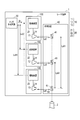
本発明の第1の実施形態に係るレーザ装置1は、図1に示すように、複数の半導体レーザ10と、複数の半導体レーザ10にそれぞれ駆動電流Idを供給する駆動装置20と、駆動電流Idを出力させるトリガ信号Stを駆動装置20に送信するトリガ生成回路30と、複数の半導体レーザ10からそれぞれ出射されたレーザ光を合波する合波装置40とを備える。合波された光は受光デバイス2に入射される。受光デバイス2は例えば光ファイバーであり、合波装置40は光ファイバーのコア部に合波された光を入射させる。
本発明の第1の実施形態に係るレーザ装置1は、図1に示すように、複数の半導体レーザ10と、複数の半導体レーザ10にそれぞれ駆動電流Idを供給する駆動装置20と、駆動電流Idを出力させるトリガ信号Stを駆動装置20に送信するトリガ生成回路30と、複数の半導体レーザ10からそれぞれ出射されたレーザ光を合波する合波装置40とを備える。合波された光は受光デバイス2に入射される。受光デバイス2は例えば光ファイバーであり、合波装置40は光ファイバーのコア部に合波された光を入射させる。
ここでは、レーザ装置1に含まれる半導体レーザ10の個数が3個(半導体レーザ11、12、13)である場合について例示的に説明する。なお、半導体レーザ10の個数が3個に限られないことはもちろんである。
以下において、トリガ生成回路30から駆動装置20までトリガ信号Stが伝播する経路を「信号経路Ls」という。つまり、信号経路Lsは、トリガ生成回路30のトリガ信号Stの送信端子から駆動装置20のトリガ信号Stを受信する受信端子までの経路をいう。例えば、駆動装置20がトランジスタである場合、トランジスタの制御電極(ゲート電極など)が受信端子である。図1において、信号経路Lsを一点鎖線で示した(以下において同様。)。
また、駆動装置20から半導体レーザ10まで駆動電流Idが伝播する経路を「電流経路Le」という。つまり、電流経路Leは、駆動装置20の駆動電流Idを出力する出力端子から半導体レーザ10の駆動電流Idが入力する入力端子までの経路をいう。例えば、半導体レーザ10のアノード端子が入力端子である。図1において、電流経路Leを実線で示した(以下において同様。)。
更に、半導体レーザ10の出射口から合波端50までレーザ光が伝播する経路を「光学経路Lp」という。図1において、光学経路Lpを破線で示した(以下において同様。)。光学経路Lpは、合波装置40を経由する。合波装置40には、例えば図1に示すように、レーザ光の進行方向を変化させる素子などの光学素子41が含まれてもよい。光学素子41は、例えばプリズム、反射レンズ、光学用ミラーなどである。
上記のように、信号経路Ls、電流経路Le及び光学経路Lpを含んで構成される複数の伝播経路Laがレーザ装置1に定義される。1つの伝播経路Laは、複数の半導体レーザ10のいずれかから出射されるレーザ光の光路をそれぞれ1つ含む。
レーザ装置1においては、信号経路Lsをトリガ信号Stが伝播する信号伝播時間Ts、電流経路Leを駆動電流Idが伝播する電流伝播時間Te、及び光学経路Lpをレーザ光が伝播する光伝播時間Tpの合計時間(以下において、「総伝播時間Ta」という。)が、トリガ生成回路30からトリガ信号Stが出力されてから半導体レーザ10から出射されたレーザ光が合波端50に到達するまでの時間である。
したがって、それぞれの半導体レーザ10から出射されたレーザ光が合波端50に到達するタイミングに影響を与えるのは、信号伝播時間Ts、電流伝播時間Te、及び光伝播時間Tpである。
レーザ装置1では、半導体レーザ10からそれぞれ出射されたレーザ光が所定のタイミングで合波端50に到達するように、複数の伝播経路Laのそれぞれについて総伝播時間Taが設定されている。即ち、レーザ装置1では、総伝播時間Taが複数の伝播経路Laのそれぞれに設定された時間であるように、信号伝播時間Ts、電流伝播時間Te及び光伝播時間Tpの少なくともいずれかが調整されている。
以下では、複数の半導体レーザ10から出射されたレーザ光が同一のタイミングで合波端50に到達するように設定されたレーザ装置1について説明する。つまり、総伝播時間Taが複数の伝播経路Laで同一であるように、信号伝播時間Ts、電流伝播時間Te及び光伝播時間の少なくともいずれかが調整される。
図1に示したレーザ装置1では、1つのトリガ生成回路30に1つの駆動装置20が接続されている。そして、駆動装置20に複数の半導体レーザ10が直列接続されている。駆動装置20から出力された駆動電流Idは、複数の半導体レーザ10に順次供給される。即ち、駆動装置20に近い側に接続された半導体レーザ11、12、13の順に駆動電流Idが供給される。
したがって、図1に示したレーザ装置1では、伝播経路Laそれぞれにおける信号経路Lsが共通であり、信号伝播時間Tsは同一である。
一方、電流経路Leはそれぞれの伝播経路Laごとに異なる。即ち、直列接続された複数の半導体レーザ10においては、駆動装置20に近い側に接続された半導体レーザ10ほど電流経路Leが短く、電流伝播時間Teが短い。
このため、図1に示したレーザ装置1では、駆動装置20に近い側に接続された半導体レーザ10の出射するレーザ光の光路を含む伝播経路Laほど、光学経路Lpが長く設定される。このようにして、電流経路Leの差が相殺されるように光学経路Lpを設定することによって、総伝播時間Taがそれぞれの伝播経路Laで同一になるように調整されている。その結果、半導体レーザ10からそれぞれ出射されるレーザ光が合波端50に到達するタイミングが一致する。これにより、レーザ装置1を高出力化できる。
具体的には、以下のように伝播経路Laが設定される。図1に示すレーザ装置1の半導体レーザ11、12、13の出射するレーザ光の光路をそれぞれ含む伝播経路La1、La2、La3の電流経路Leの長さをLe1、Le2、Le3とすると、Le1<Le2<Le3である。ここで、駆動電流Idの伝播速度を電流伝播速度Veとすると、長さがLe1、Le2、Le3の電流経路Leにおける電流伝播時間Te1、Te2、Te3は、Le1/Ve、Le2/Ve、Le3/Veである。
このとき、長さがLe1、Le2、Le3の電流経路Leを駆動電流Idが伝播する電流伝播時間Teの差を相殺するように、伝播経路La1、La2、La3の光学経路Lpの長さであるLp1、Lp2、Lp3が設定される。即ち、Lp1>Lp2>Lp3とする。光学経路Lpにおけるレーザ光の伝播速度を光伝播速度Vpとすると、長さがLp1、Lp2、Lp3の光学経路Lpおける電流伝播時間Tp1、Tp2、Tp3は、Lp1/Vp、Lp2/Vp、Lp3/Vpである。伝播経路La1、La2、La3の総伝播時間Taを同一にするためには、以下の式(1)が満たされる:
Te1+Tp1=Te2+Tp2=Te3+Tp3 ・・・(1)
したがって、以下の式(2)を満たすように、Lp1、Lp2、Lp3が設定される:
Le1/Ve+Lp1/Vp=Le2/Ve+Lp2/Vp=Le3/Ve+Lp3/Vp ・・・(2)
Te1+Tp1=Te2+Tp2=Te3+Tp3 ・・・(1)
したがって、以下の式(2)を満たすように、Lp1、Lp2、Lp3が設定される:
Le1/Ve+Lp1/Vp=Le2/Ve+Lp2/Vp=Le3/Ve+Lp3/Vp ・・・(2)
なお、図1に示したレーザ装置1では、伝播経路Laにおける半導体レーザ10の出射口から光学素子41までの距離Lp0を同一としている。半導体レーザ10から出射されたレーザ光は光学素子41で反射された後、受光デバイス2に向けて進行する。そして、図1に示したように、伝播経路La3の光学素子41において半導体レーザ11、12、13から出射されたレーザ光が合波される。伝播経路La1における光学素子41から合波端50までの距離Lp01として、Lp1=Lp0+Lp01である。また、伝播経路La2における光学素子41から合波端50までの距離Lp02として、Lp2=Lp0+Lp02である。伝播経路La3では、Lp3=Lp0である。
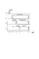
そして、伝播経路Laごとに光学素子41から合波端50までの距離を調整することによって、伝播経路La1、La2、La3の総伝播時間Taを一致させる。ここで、長さLe1と長さLe2との差をLe02、長さLe1と長さLe3との差をLe03として、総伝播時間Taを一致させる例を説明する。この場合における、半導体レーザ11に駆動電流Idが供給された時刻t1を基準としたタイミングチャートの例を図2に示す。
図2の時刻t1において、半導体レーザ11からレーザ光L1が出射される。その後、時刻t1から時間Le02/Veを経過した後の時刻t2において、半導体レーザ12に駆動電流Idが供給され、半導体レーザ12からレーザ光L2が出射される。更に、時刻t1から時間Le03/Veを経過した後の時刻t3において、半導体レーザ13に駆動電流Idが供給され、半導体レーザ13からレーザ光L3が出射される。
一方、時刻t1から時間(Lp0+Lp01)/Vpを経過した後の時刻t4において、半導体レーザ11から出射されたレーザ光L1が合波端50に到達する。また、時刻t2から(Lp0+Lp02)/Vpを経過した後の時刻t4において、半導体レーザ12から出射されたレーザ光L2が合波端50に到達する。更に、時刻t3から時間Lp0/Vpを経過した後の時刻t4において、半導体レーザ13から出射されたレーザ光L3が合波端50に到達する。
つまり、以下の式(3)を満足するように、電流経路Leの差Le02、Le03に対応して光学経路の差Lp01、Lp02が設定される:
(Lp0+Lp01)/Vp=Le02/Ve+(Lp0+Lp02)/Vp=Le03/Ve+Lp0/Vp ・・・(3)
(Lp0+Lp01)/Vp=Le02/Ve+(Lp0+Lp02)/Vp=Le03/Ve+Lp0/Vp ・・・(3)
上記では、伝播経路Laごとに光学素子41から合波端50までの距離を調整する例を説明した。しかし、半導体レーザ10の出射口から光学素子41までの距離を調整したり、半導体レーザ10の出射口から光学素子41までの距離と光学素子41から合波端50までの距離の両方を調整したりしてもよいことはもちろんである。
上記のようにすべての伝播経路Laの総伝播時間Taを同一にすることによって、半導体レーザ11、12、13からそれぞれ出射されるレーザ光が合波端50に到達するタイミングを一致させることができる。その結果、レーザ装置1を高出力化できる。
上記では、電流経路Leの長さの差を光学経路Lpの差で相殺する例を示した。しかし、光学経路Lpの長さに差がある場合に、電流経路Leの長さを調整してもよいことはもちろんである。
図1に示したレーザ装置1によれば、駆動装置20に半導体レーザ10を直列接続することによって消費電力を抑制することができる。
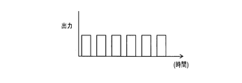
ところで、上記では、それぞれの伝播経路Laで総伝播時間Taが同一であるように設定する場合を説明した。これにより、半導体レーザ10のそれぞれのレーザ光が合波端50に到達するタイミングを一致させ、レーザ装置1を高出力化できる。しかし、半導体レーザ10ごとに伝播経路Laの長さを変えて、半導体レーザ10のそれぞれのレーザ光が合波端50に到達するタイミングを互いに異なるようにしてもよい。即ち、半導体レーザ10ごとに、所定の値だけずれるように総伝播時間を設定する。これにより、例えば図3に示すように、トリガ生成回路30の送信するトリガ信号Stの周期よりも短い一定の周期で、半導体レーザ10のレーザ光を受光デバイス2に入射できる。これにより、例えば複数の半導体レーザ10のレーザ光を合波した高出力は必要としないが、短い周期でレーザ光を照射することが必要なレーザ加工などにレーザ装置1を使用できる。
<変形例>
上記では、光学経路Lpの物理的な長さを設定して光伝播時間Tpを調整する場合を説明したが、他の方法によって光伝播時間Tpを調整してもよい。例えば、図4に示すように、レーザ光Lが進行する光学経路Lp上にガラス板42などのレーザ光Lの進行速度を低下させる光学素子を配置する。このようにして、光学経路Lpごとにレーザ光の光伝播速度Vpを変更し、伝播経路Laごとに光伝播時間Tpに差を設定してもよい。
上記では、光学経路Lpの物理的な長さを設定して光伝播時間Tpを調整する場合を説明したが、他の方法によって光伝播時間Tpを調整してもよい。例えば、図4に示すように、レーザ光Lが進行する光学経路Lp上にガラス板42などのレーザ光Lの進行速度を低下させる光学素子を配置する。このようにして、光学経路Lpごとにレーザ光の光伝播速度Vpを変更し、伝播経路Laごとに光伝播時間Tpに差を設定してもよい。
或いは、電流経路Leの長さを調整する以外に、伝播経路Laごとに駆動電流Idの電流伝播速度Veが異なるように、材料や形状(パターン)の異なる導線を電流経路Leに採用してもよい。即ち、伝播経路Laそれぞれの電流経路Leに駆動電流Idの電流伝播速度Veが互いに異なる導線を使用することによって、伝播経路Laごとに電流伝播時間Teに差を設定する。
例えば、伝播経路Laが長い電流経路Leほど、電流伝播時間Teが小さいように導線の誘電率を設定する。これにより、伝播経路La間の信号伝播時間Tsと光伝播時間Tpの合計の差異と、電流伝播時間Teとの差異とが一定程度相殺される。例えば、トリガ生成回路30に近い位置の駆動装置20ほど、電流伝播速度Veの遅い導線を電流経路Leに使用する。
このように、誘電率の異なる材料の導線や膜厚や幅の異なる形状の導線を使用して、複数の伝播経路Laのそれぞれについて電流伝播時間Teを調整してもよい。ただし、導線の材料や形状の差による電流伝播速度の差は小さい。このため、光学経路Lpの長さによって信号経路Lsの長さの差を略一致させ、導線の材料や形状の差による電流伝播速度の差の効果は微調整に使用することが好ましい。
(第2の実施形態)
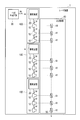
本発明の第2の実施形態に係るレーザ装置1では、図5に示すように、1つのトリガ生成回路30に複数の駆動装置20が接続され、駆動装置20のそれぞれに半導体レーザ10が接続されている。即ち、駆動装置20と半導体レーザ10とをそれぞれ1つずつ含む複数のレーザユニット100のレーザ光を出射するタイミングが、共通のトリガ生成回路30によって制御される構成である。ここで、各レーザユニット100において、電流経路Leの長さは同じであり、電流伝播時間Teは同一であるとする。他は、図1に示したレーザ装置1と同様である。
本発明の第2の実施形態に係るレーザ装置1では、図5に示すように、1つのトリガ生成回路30に複数の駆動装置20が接続され、駆動装置20のそれぞれに半導体レーザ10が接続されている。即ち、駆動装置20と半導体レーザ10とをそれぞれ1つずつ含む複数のレーザユニット100のレーザ光を出射するタイミングが、共通のトリガ生成回路30によって制御される構成である。ここで、各レーザユニット100において、電流経路Leの長さは同じであり、電流伝播時間Teは同一であるとする。他は、図1に示したレーザ装置1と同様である。
図5に示したレーザ装置1では、信号経路Lsがそれぞれの伝播経路Laごとに異なる。即ち、トリガ生成回路30に近い位置に配置されたレーザユニット100ほど信号経路Lsが短く、信号伝播時間Tsが短い。つまり、駆動装置21、22、23の順にトリガ信号Stを受信する。その結果、半導体レーザ11、12、13の順に駆動電流Idが供給される。
このため、図5に示したレーザ装置1では、トリガ生成回路30の近くに配置されたレーザユニット100から出射されるレーザ光の光路を含む伝播経路Laほど、信号経路Lsの差が相殺されるように光学経路Lpが長く設定される。このようにして、総伝播時間Taがそれぞれの伝播経路Laで同一になるように設定される。その結果、半導体レーザ10からそれぞれ出射されるレーザ光が合波端50に到達するタイミングが一致する。これにより、レーザ装置1を高出力化できる。
具体的には、以下のように伝播経路Laが設定される。図5に示すレーザ装置1の半導体レーザ11、12、13をそれぞれ含む伝播経路La1、La2、La3の信号経路Lsの長さをLs1、Ls2、Ls3とすると、Ls1<Ls2<Ls3である。ここで、トリガ信号Stの伝播速度を信号伝播速度Vsとすると、長さがLs1、Ls2、Ls3の信号経路Lsにおける信号伝播時間Ts1、Ts2、Ts3は、Ls1/Vs、Ls2/Vs、Ls3/Vsである。
このとき、長さがLs1、Ls2、Ls3の信号経路Lsをトリガ信号Stが伝播する信号伝播時間Tsの差を相殺するように、伝播経路La1、La2、La3の光学経路Lpの長さであるLp1、Lp2、Lp3が設定される。即ち、Lp1>Lp2>Lp3とする。長さがLp1、Lp2、Lp3の光学経路Lpおける電流伝播時間Tp1、Tp2、Tp3は、Lp1/Vp、Lp2/Vp、Lp3/Vpである。このため、伝播経路La1、La2、La3の総伝播時間Taを同一にするためには、以下の式(4)が満たされる:
Ts1+Tp1=Ts2+Tp2=Ts3+Tp3 ・・・(4)
したがって、以下の式(5)を満たすように、Lp1、Lp2、Lp3が設定される:
Ls1/Vs+Lp1/Vp=Ls2/Vs+Lp2/Vp=Ls3/Vs+Lp3/Vp ・・・(5)
Ts1+Tp1=Ts2+Tp2=Ts3+Tp3 ・・・(4)
したがって、以下の式(5)を満たすように、Lp1、Lp2、Lp3が設定される:
Ls1/Vs+Lp1/Vp=Ls2/Vs+Lp2/Vp=Ls3/Vs+Lp3/Vp ・・・(5)
なお、図5に示したレーザ装置1では、図1に示したレーザ装置1と同様に、伝播経路Laにおける半導体レーザ10の出射口から光学素子41までの距離Lp0は同一であり、Lp1=Lp0+Lp01、Lp2=Lp0+Lp02、Lp3=Lp0である。
そして、伝播経路Laごとに光学素子41から合波端50までの距離を調整することによって、伝播経路La1~La3の総伝播時間Taを一致させる。ここで、長さLs1と長さLs2との差をLs02、長さLs1と長さLs3との差をLs03として、総伝播時間Taを一致させる例を説明する。この場合における、信号経路Lsの長さがLs1である駆動装置21にトリガ信号Stが送信された時刻t0を基準としたタイミングチャートの例を図6に示す。
図6の時刻t0から時間Ls0/Vsを経過した後の時刻t1において、半導体レーザ11からレーザ光L1が出射される。その後、時刻t1から時間Ls02/Vsを経過した後の時刻t2において、半導体レーザ12からレーザ光L2が出射される。更に、時刻t1から時間Ls03/Vsを経過した後の時刻t3において、半導体レーザ13からレーザ光L3が出射される。
一方、時刻t1から時間(Lp0+Lp01)/Vpを経過した後の時刻t4において、半導体レーザ11から出射されたレーザ光L1が合波端50に到達する。また、時刻t2から(Lp0+Lp02)/Vpを経過した後の時刻t4において、半導体レーザ12から出射されたレーザ光L2が合波端50に到達する。更に、時刻t3から時間Lp0/Vpを経過した後の時刻t4において、半導体レーザ13から出射されたレーザ光L3が合波端50に到達する。
つまり、以下の式(6)を満足するように、信号経路Lsの差Ls02、Ls03に対応して光学経路の差Lp01、Lp02が設定される:
(Lp0+Lp01)/Vp=Ls02/Vs+(Lp0+Lp02)/Vp=Ls03/Vs+Lp0/Vp ・・・(6)
(Lp0+Lp01)/Vp=Ls02/Vs+(Lp0+Lp02)/Vp=Ls03/Vs+Lp0/Vp ・・・(6)
上記では、伝播経路Laごとに光学素子41から合波端50までの距離を調整する例を説明した。しかし、半導体レーザ10の出射口から光学素子41までの距離を調整したり、半導体レーザ10の出射口から光学素子41までの距離と光学素子41から合波端50までの距離の両方を調整したりしてもよいことはもちろんである。
上記のようにすべての伝播経路Laの総伝播時間Taを同一にすることによって、半導体レーザ11、12、13からそれぞれ出射されるレーザ光が合波端50に到達するタイミングを一致させることができる。その結果、レーザ装置1を高出力化できる。なお、半導体レーザ10から出力されたレーザ光のそれぞれが異なるタイミングで合波端50に到達するようにしてもよいことは、第1の実施形態と同様である。
図5に示したレーザ装置1によれば、共通のトリガ生成回路30に複数のレーザユニット100を並列に接続することによって、複数の半導体レーザ10を高速に制御することができる。なお、第1の実施形態の変形例で説明したように、光学経路Lpごとにレーザ光の光伝播速度Vpを変更して光伝播時間Tpを調整してもよい。
また、信号経路Lsの長さの差を光学経路Lpの長さで相殺する例を示した。しかし、光学経路Lpの長さに差がある場合に、信号経路Lsの長さを調整してもよいことはもちろんである。
<変形例>
信号経路Lsの差を相殺するように、レーザユニット100ごとに、駆動装置20と半導体レーザ10間の電流経路Leを設定してもよい。即ち、信号経路Lsの長いレーザユニット100ほど、電流経路Leを短くする。このように、信号伝播時間Tsの差異を電流伝播時間Teによっても相殺できる。或いは、信号伝播時間Tsの差異を、電流伝播時間Teと光伝播時間Tpの両方によって相殺してもよいことはもちろんである。
信号経路Lsの差を相殺するように、レーザユニット100ごとに、駆動装置20と半導体レーザ10間の電流経路Leを設定してもよい。即ち、信号経路Lsの長いレーザユニット100ほど、電流経路Leを短くする。このように、信号伝播時間Tsの差異を電流伝播時間Teによっても相殺できる。或いは、信号伝播時間Tsの差異を、電流伝播時間Teと光伝播時間Tpの両方によって相殺してもよいことはもちろんである。
例えば、駆動装置21と半導体レーザ11間の電流経路Leの長さと駆動装置22と半導体レーザ12間の電流経路Leの長さとの差をLe02、駆動装置21と半導体レーザ11間の電流経路Leの長さと駆動装置23と半導体レーザ13間の電流経路Leの長さとの差をLe03とする。このとき、以下の式(7)を満たすように、伝播経路Laごとに信号経路Ls、電流経路Le及び光学経路Lpを設定する:
(Lp0+Lp01)/Vp=Ls02/Vs+Le02/Ve+(Lp0+Lp02)/Vp=Ls03/Vs+Le03/Ve+Lp0/Vp ・・・(7)
(Lp0+Lp01)/Vp=Ls02/Vs+Le02/Ve+(Lp0+Lp02)/Vp=Ls03/Vs+Le03/Ve+Lp0/Vp ・・・(7)
式(7)を満たすことにより、すべての伝播経路Laで総伝播時間Taを同一にできる。その結果、半導体レーザ11、12、13からそれぞれ出射されるレーザ光が合波端50に到達するタイミングを一致させることができる。
他は第1の実施形態と実質的に同様であり、重複した記載を省略する。
(その他の実施形態)
上記のように、本発明は実施形態によって記載したが、この開示の一部をなす論述及び図面はこの発明を限定するものであると理解すべきではない。この開示から当業者には様々な代替実施形態、実施例及び運用技術が明らかとなろう。
上記のように、本発明は実施形態によって記載したが、この開示の一部をなす論述及び図面はこの発明を限定するものであると理解すべきではない。この開示から当業者には様々な代替実施形態、実施例及び運用技術が明らかとなろう。
例えば図7に示すように、複数の半導体レーザ10がそれぞれ直列に接続された駆動装置20からなるレーザユニット100を複数有するレーザ装置1においても、本発明は適用可能である。上記のような複数のレーザユニット100に同一のトリガ生成回路30からトリガ信号Stを送信する構成のレーザ装置1についても、伝播経路Laのそれぞれについて総伝播時間Taが設定された時間であるように、信号伝播時間Ts、電流伝播時間Te及び光伝播時間Tpのすくなくともいずれかについて調整される。
即ち、レーザユニット100内での電流経路Leの差を相殺するように光学経路Lpを調整したり、レーザユニット100間での光学経路Lpの差を相殺するように電流経路Leを調整したりする。また、レーザユニット100間での信号経路Lsの差を相殺するように光学経路Lp、電流経路Leのいずれか、或いは両方が調整される。
このように、本発明はここでは記載していない様々な実施形態等を含むことは勿論である。したがって、本発明の技術的範囲は上記の説明から妥当な請求の範囲に係る発明特定事項によってのみ定められるものである。
本発明は、複数の半導体レーザのレーザ光を合波するレーザ装置に利用可能である。
Claims (7)
- 複数の半導体レーザと、
前記複数の半導体レーザに駆動電流を供給する駆動装置と、
前記駆動電流を出力させるトリガ信号を前記駆動装置に送信するトリガ生成回路と、
前記複数の半導体レーザ10からそれぞれ出射されたレーザ光を合波端で合波させる合波装置と
を備え、
前記複数の半導体レーザのいずれかから出射される前記レーザ光の光路をそれぞれ1つ含む伝播経路であって、前記トリガ生成回路から前記駆動装置まで前記トリガ信号が伝播する信号経路、前記駆動装置から前記半導体レーザまで前記駆動電流が伝播する電流経路、及び前記半導体レーザの出射口から前記合波端まで前記レーザ光が伝播する光学経路を含んで構成される複数の前記伝播経路が定義され、
前記信号経路を前記トリガ信号が伝播する信号伝播時間、前記電流経路を前記駆動電流が伝播する電流伝播時間、及び前記光学経路を前記レーザ光が伝播する光伝播時間の合計時間が複数の前記伝播経路のそれぞれに設定された時間であるように、前記信号伝播時間、前記電流伝播時間及び前記光伝播時間の少なくともいずれかが調整されていることを特徴とするレーザ装置。 - 前記合計時間が複数の前記伝播経路で同一であるように、前記信号伝播時間、前記電流伝播時間及び前記光伝播時間の少なくともいずれかが調整されていることを特徴とする請求項1に記載のレーザ装置。
- 前記複数の半導体レーザから出力された前記レーザ光のそれぞれが異なるタイミングで前記合波端に到達するように、前記信号伝播時間、前記電流伝播時間及び前記光伝播時間の少なくともいずれかが調整されていることを特徴とする請求項1に記載のレーザ装置。
- 前記駆動電流が前記複数の半導体レーザに順次供給されるように前記複数の半導体レーザが直列接続され、
前記電流経路が短くて前記駆動電流が先に供給される前記半導体レーザから出射されるレーザ光の光路を含む前記伝播経路ほど、前記光学経路が長く設定されていることを特徴とする請求項1に記載のレーザ装置。 - 同一の前記トリガ生成回路から前記トリガ信号を送信される複数の前記駆動装置を備え、
前記信号経路が短くて前記トリガ信号を先に受信する前記駆動装置を含む前記伝播経路ほど、前記光学経路が長く設定されていることを特徴とする請求項1に記載のレーザ装置。 - 前記伝播経路それぞれの前記電流経路に前記駆動電流の伝播速度が互いに異なる導線を使用することによって、前記伝播経路ごとに前記電流伝播時間に差を設定したことを特徴とする請求項1に記載のレーザ装置。
- 前記光学経路に前記レーザ光の進行速度を低下させる光学素子を配置することによって、前記伝播経路ごとに前記光伝播時間に差を設定したことを特徴とする請求項1に記載のレーザ装置。
Priority Applications (2)
| Application Number | Priority Date | Filing Date | Title |
|---|---|---|---|
| US15/129,061 US9647422B1 (en) | 2014-03-26 | 2014-03-26 | Laser device |
| PCT/JP2014/058478 WO2015145603A1 (ja) | 2014-03-26 | 2014-03-26 | レーザ装置 |
Applications Claiming Priority (1)
| Application Number | Priority Date | Filing Date | Title |
|---|---|---|---|
| PCT/JP2014/058478 WO2015145603A1 (ja) | 2014-03-26 | 2014-03-26 | レーザ装置 |
Publications (1)
| Publication Number | Publication Date |
|---|---|
| WO2015145603A1 true WO2015145603A1 (ja) | 2015-10-01 |
Family
ID=54194201
Family Applications (1)
| Application Number | Title | Priority Date | Filing Date |
|---|---|---|---|
| PCT/JP2014/058478 Ceased WO2015145603A1 (ja) | 2014-03-26 | 2014-03-26 | レーザ装置 |
Country Status (2)
| Country | Link |
|---|---|
| US (1) | US9647422B1 (ja) |
| WO (1) | WO2015145603A1 (ja) |
Citations (7)
| Publication number | Priority date | Publication date | Assignee | Title |
|---|---|---|---|---|
| JPS6328089A (ja) * | 1986-07-22 | 1988-02-05 | Iwatsu Electric Co Ltd | 半導体レ−ザ光パルス発生器 |
| JPH03104331A (ja) * | 1989-09-06 | 1991-05-01 | General Instr Corp | アナログ光通信システムにおけるひずみ減少装置と方式 |
| JPH09168884A (ja) * | 1995-12-19 | 1997-06-30 | Mitsubishi Chem Corp | レーザテキスチャ装置 |
| JP2008244339A (ja) * | 2007-03-28 | 2008-10-09 | Sumitomo Osaka Cement Co Ltd | 光パルスレーザー装置 |
| JP2011061153A (ja) * | 2009-09-14 | 2011-03-24 | Omron Corp | レーザ加工装置およびレーザ加工方法 |
| JP2012018122A (ja) * | 2010-07-09 | 2012-01-26 | Olympus Corp | 観察装置 |
| US20120243562A1 (en) * | 2011-03-21 | 2012-09-27 | Soreq Nuclear Research Center | Laser Diode Driver |
Family Cites Families (3)
| Publication number | Priority date | Publication date | Assignee | Title |
|---|---|---|---|---|
| US5946334A (en) * | 1996-03-27 | 1999-08-31 | Ricoh Company, Inc. | Semiconductor laser control system |
| CN101263422B (zh) * | 2005-09-14 | 2010-09-22 | 松下电器产业株式会社 | 激光图像形成装置 |
| JP2013048159A (ja) | 2011-08-29 | 2013-03-07 | Furukawa Electric Co Ltd:The | レーザ加工装置 |
-
2014
- 2014-03-26 WO PCT/JP2014/058478 patent/WO2015145603A1/ja not_active Ceased
- 2014-03-26 US US15/129,061 patent/US9647422B1/en not_active Expired - Fee Related
Patent Citations (7)
| Publication number | Priority date | Publication date | Assignee | Title |
|---|---|---|---|---|
| JPS6328089A (ja) * | 1986-07-22 | 1988-02-05 | Iwatsu Electric Co Ltd | 半導体レ−ザ光パルス発生器 |
| JPH03104331A (ja) * | 1989-09-06 | 1991-05-01 | General Instr Corp | アナログ光通信システムにおけるひずみ減少装置と方式 |
| JPH09168884A (ja) * | 1995-12-19 | 1997-06-30 | Mitsubishi Chem Corp | レーザテキスチャ装置 |
| JP2008244339A (ja) * | 2007-03-28 | 2008-10-09 | Sumitomo Osaka Cement Co Ltd | 光パルスレーザー装置 |
| JP2011061153A (ja) * | 2009-09-14 | 2011-03-24 | Omron Corp | レーザ加工装置およびレーザ加工方法 |
| JP2012018122A (ja) * | 2010-07-09 | 2012-01-26 | Olympus Corp | 観察装置 |
| US20120243562A1 (en) * | 2011-03-21 | 2012-09-27 | Soreq Nuclear Research Center | Laser Diode Driver |
Also Published As
| Publication number | Publication date |
|---|---|
| US9647422B1 (en) | 2017-05-09 |
| US20170110849A1 (en) | 2017-04-20 |
Similar Documents
| Publication | Publication Date | Title |
|---|---|---|
| US7489711B2 (en) | Laser beam processing apparatus | |
| ATE545827T1 (de) | Kompaktes fahrzeugbeleuchtungssystem mit mehreren strahlenbündeln | |
| US9952441B2 (en) | Optical module | |
| DK2184868T3 (da) | Optisk multimode-system | |
| CN102132207A (zh) | 太赫兹波产生装置以及太赫兹波产生方法 | |
| EP4481433A3 (en) | Waveguide diffusers for lidars | |
| WO2018194301A1 (ko) | 레이저 증폭 장치 | |
| WO2009025261A1 (ja) | マルチビーム走査装置 | |
| WO2019144495A1 (zh) | 激光合光装置及显示设备 | |
| CN107005017A (zh) | 光纤激光器系统以及激光输出方法 | |
| CN108535943A (zh) | 一种光源装置及其投影显示系统 | |
| US9164352B2 (en) | System and method for synchronizing light pulses at a selected location | |
| WO2021079703A1 (ja) | 光給電システム | |
| WO2015145603A1 (ja) | レーザ装置 | |
| CN104037615A (zh) | 高功率脉冲可裁剪式固体激光器 | |
| CN109194408B (zh) | 一种空间激光通信发射装置 | |
| CN104993367B (zh) | 无线激光通信ppm调制器及其多光源序列合成的方法 | |
| CN101581436B (zh) | Led发光系统及发光方法 | |
| US20180323567A1 (en) | Laser beam generation apparatus, laser machining device, and laser machining method | |
| US20090179492A1 (en) | Pluggable optical transceiver with function to be provided with power supplies simultaneously | |
| CN107888293A (zh) | 光模块 | |
| CN209387865U (zh) | 一种激光雷达发射装置及激光雷达 | |
| WO2017081858A1 (en) | Laser beam generation apparatus, laser machining device, and laser machining method | |
| JP2017103448A (ja) | レーザー光発生装置、レーザー加工機、被加工物の生産方法 | |
| WO2016001969A1 (ja) | 半導体レーザ装置 |
Legal Events
| Date | Code | Title | Description |
|---|---|---|---|
| 121 | Ep: the epo has been informed by wipo that ep was designated in this application |
Ref document number: 14887290 Country of ref document: EP Kind code of ref document: A1 |
|
| NENP | Non-entry into the national phase |
Ref country code: DE |
|
| WWE | Wipo information: entry into national phase |
Ref document number: 15129061 Country of ref document: US |
|
| 122 | Ep: pct application non-entry in european phase |
Ref document number: 14887290 Country of ref document: EP Kind code of ref document: A1 |
|
| NENP | Non-entry into the national phase |
Ref country code: JP |