WO2015137144A1 - 固体撮像素子 - Google Patents
固体撮像素子 Download PDFInfo
- Publication number
- WO2015137144A1 WO2015137144A1 PCT/JP2015/055723 JP2015055723W WO2015137144A1 WO 2015137144 A1 WO2015137144 A1 WO 2015137144A1 JP 2015055723 W JP2015055723 W JP 2015055723W WO 2015137144 A1 WO2015137144 A1 WO 2015137144A1
- Authority
- WO
- WIPO (PCT)
- Prior art keywords
- pixel
- channel
- unit
- image signal
- pixels
- Prior art date
- Legal status (The legal status is an assumption and is not a legal conclusion. Google has not performed a legal analysis and makes no representation as to the accuracy of the status listed.)
- Ceased
Links
Images






Classifications
-
- H—ELECTRICITY
- H04—ELECTRIC COMMUNICATION TECHNIQUE
- H04N—PICTORIAL COMMUNICATION, e.g. TELEVISION
- H04N9/00—Details of colour television systems
- H04N9/64—Circuits for processing colour signals
- H04N9/646—Circuits for processing colour signals for image enhancement, e.g. vertical detail restoration, cross-colour elimination, contour correction, chrominance trapping filters
-
- G—PHYSICS
- G06—COMPUTING OR CALCULATING; COUNTING
- G06T—IMAGE DATA PROCESSING OR GENERATION, IN GENERAL
- G06T3/00—Geometric image transformations in the plane of the image
- G06T3/40—Scaling of whole images or parts thereof, e.g. expanding or contracting
-
- H—ELECTRICITY
- H04—ELECTRIC COMMUNICATION TECHNIQUE
- H04N—PICTORIAL COMMUNICATION, e.g. TELEVISION
- H04N23/00—Cameras or camera modules comprising electronic image sensors; Control thereof
- H04N23/10—Cameras or camera modules comprising electronic image sensors; Control thereof for generating image signals from different wavelengths
- H04N23/12—Cameras or camera modules comprising electronic image sensors; Control thereof for generating image signals from different wavelengths with one sensor only
-
- H—ELECTRICITY
- H04—ELECTRIC COMMUNICATION TECHNIQUE
- H04N—PICTORIAL COMMUNICATION, e.g. TELEVISION
- H04N23/00—Cameras or camera modules comprising electronic image sensors; Control thereof
- H04N23/50—Constructional details
- H04N23/51—Housings
-
- H—ELECTRICITY
- H04—ELECTRIC COMMUNICATION TECHNIQUE
- H04N—PICTORIAL COMMUNICATION, e.g. TELEVISION
- H04N23/00—Cameras or camera modules comprising electronic image sensors; Control thereof
- H04N23/80—Camera processing pipelines; Components thereof
- H04N23/84—Camera processing pipelines; Components thereof for processing colour signals
- H04N23/843—Demosaicing, e.g. interpolating colour pixel values
-
- H—ELECTRICITY
- H04—ELECTRIC COMMUNICATION TECHNIQUE
- H04N—PICTORIAL COMMUNICATION, e.g. TELEVISION
- H04N23/00—Cameras or camera modules comprising electronic image sensors; Control thereof
- H04N23/80—Camera processing pipelines; Components thereof
- H04N23/84—Camera processing pipelines; Components thereof for processing colour signals
- H04N23/86—Camera processing pipelines; Components thereof for processing colour signals for controlling the colour saturation of colour signals, e.g. automatic chroma control circuits
-
- H—ELECTRICITY
- H04—ELECTRIC COMMUNICATION TECHNIQUE
- H04N—PICTORIAL COMMUNICATION, e.g. TELEVISION
- H04N25/00—Circuitry of solid-state image sensors [SSIS]; Control thereof
- H04N25/10—Circuitry of solid-state image sensors [SSIS]; Control thereof for transforming different wavelengths into image signals
- H04N25/11—Arrangement of colour filter arrays [CFA]; Filter mosaics
- H04N25/13—Arrangement of colour filter arrays [CFA]; Filter mosaics characterised by the spectral characteristics of the filter elements
- H04N25/134—Arrangement of colour filter arrays [CFA]; Filter mosaics characterised by the spectral characteristics of the filter elements based on three different wavelength filter elements
-
- H—ELECTRICITY
- H04—ELECTRIC COMMUNICATION TECHNIQUE
- H04N—PICTORIAL COMMUNICATION, e.g. TELEVISION
- H04N9/00—Details of colour television systems
- H04N9/03—Circuitry for demodulating colour component signals modulated spatially by colour striped filters by frequency separation
Definitions
- the present invention relates to a solid-state imaging device.
- pixel data of an original image having a predetermined color arrangement (below, also referred to as a Bayer arrangement since a Bayer arrangement is common) is used to perform a filtering process in units of lines to obtain luminance data and color difference data.
- a solid-state imaging device is known that extracts two sets of data, resizes the extracted luminance data and color difference data by independently applying a band limiting filter, and then reconstructs the original Bayer array. (For example, refer to Patent Document 1). According to this solid-state imaging device, the above processing maintains the sense of resolution while reducing false signals such as moire and false colors.
- FIG. 12 shows a two-dimensional spatial frequency coordinate system representing the limit band of a full-resolution Bayer image and a reduced Bayer image reduced to 1/2 in both vertical and horizontal directions.
- fs indicates the Nyquist frequency corresponding to the pixel pitch (sampling period) of the full resolution image.
- the reproduction band of the G signal in the Bayer array is a rhombus whose reproduction band in the oblique 45 ° direction is lower than that in the vertical and horizontal directions, and the reproduction band in the oblique 45 ° direction has been reduced. Furthermore, the reproduction band of the R / B signal is the same as that of the G signal in the direction of 45 ° obliquely, but the reproduction band in the vertical and horizontal directions is half that of the G signal, and can be reproduced by comparison with the G signal. The significant frequency band has been greatly reduced.
- the present invention has been made in view of the above-described circumstances, and provides a solid-state imaging device capable of obtaining a reduced full-color multi-channel signal while minimizing the reduction in the frequency band that can be reproduced originally.
- the purpose is to do.
- a photoelectric conversion unit in which pixels of a plurality of colors having a predetermined periodicity are arranged in a two-dimensional array in a color array, and a pixel signal acquired by the photoelectric conversion unit are expressed as n ⁇ a pixel mixture readout unit that mixes pixels of the same color in n (n is an arbitrary integer of 2 or more) blocks and outputs a reduced image signal of a multi-channel with a reduction ratio of 1 / n, and the pixel mixture readout unit
- n is an arbitrary integer of 2 or more
- the light from the subject incident on the photoelectric conversion unit is photoelectrically converted into an electrical image signal for each pixel periodically arranged in color, and the acquired image signal is n ⁇ n.
- Each pixel of the same color in each block is mixed in the pixel mixture reading unit, and a multi-channel reduced image signal having a reduction ratio of 1 / n is output.
- the multi-channel reduced image signal mixed for each color includes a shift according to the color arrangement of the pixels. By correcting by the inter-channel shift correction unit, a multi-channel reduced image signal with no shift is output. can do.
- the photoelectric conversion unit includes the pixels arranged in a Bayer array, and the pixel mixture readout unit coordinates the mixed pixel signals of the same color at the barycentric positions of the pixels of the same color in the block.
- the inter-channel deviation correction unit calculates a positional deviation correction unit that corrects the positional deviation of the reduced image signal so that the coordinates of the reduced image signal of each color coincide with each other when n is an even number. You may have.
- the block mixed by the pixel mixing and reading unit includes an even number of pixels
- the barycentric position of pixels of the same color in the block is shifted between colors in the image signal acquired by each pixel of the photoelectric conversion unit arranged in the Bayer array.
- the photoelectric conversion unit includes the pixels arranged in a Bayer array, and the inter-channel shift correction unit calculates a difference in characteristics of pixels of the same color between adjacent rows when n is an odd number. You may provide the gain correction
- the image signal acquired by each pixel of the photoelectric conversion unit arranged in the Bayer array is obtained between the colors at the centroid positions of the same color pixels in the block when the block mixed by the pixel mixture reading unit includes an odd number of pixels. Although there is no positional shift, it is shifted due to the difference in the spectral characteristics of the filters in the two types of G channels. According to this aspect, the gain correction unit of the channel misalignment correction unit can correct the spectral characteristic shift of the filter and output a reduced image signal of a multi-channel with less noise.
- the photoelectric conversion unit includes the pixels arranged in a Bayer array, and the pixel mixture reading unit arranges the mixed pixel signals of the same color at the center of gravity of the pixels of the same color in the block.
- the inter-channel misalignment correction unit corrects the misalignment of the reduced image signal so that the coordinates of the reduced image signal of each color coincide with each other when n is an even number.
- a gain correction unit that corrects a difference in characteristics of pixels of the same color between adjacent rows when n is an odd number.
- the channel misalignment correcting unit corrects the shift of the reduced image signal between the channels and outputs it. be able to.
- the multi-channel reduced image signal corrected by the inter-channel shift correction unit is separated into a luminance signal and a color difference signal, and a color conversion unit that limits a signal band of the color difference signal;
- a pixel thinning unit that thins out the color difference signals output from the conversion unit may be provided.
- the multi-channel reduced image signal corrected by the inter-channel misalignment correction unit is subjected to gradation conversion, and output as an image signal expressed with a bit width smaller than the bit width after AD conversion.
- a gradation conversion unit that performs the above may be provided. In this way, the amount of data output from the gradation conversion unit can be reduced.
- a pixel signal acquired by a photoelectric conversion unit formed by two-dimensionally arranging pixels of a plurality of colors having a predetermined periodicity in a color array vertically and horizontally is represented by n ⁇ n (n Is an arbitrary integer greater than or equal to 2) which is mixed for each pixel of the same color in each block and outputs a multi-channel reduced image signal with a reduction ratio of 1 / n, and is output by the pixel mixture reading unit
- a channel-to-channel shift correction unit that corrects and outputs a shift of the reduced image signal between channels.
- FIG. 1 is a block diagram illustrating a solid-state imaging device according to a first embodiment of the present invention. It is a figure which shows the pixel arrangement
- FIG. 2 is a block diagram illustrating a photoelectric conversion unit and an image reading unit of the solid-state imaging device in FIG. 1.
- FIG. 5 is a diagram illustrating R-channel pixels and their barycentric positions in the block of FIG. 4.
- FIG. 5 is a diagram illustrating G-channel pixels and their centroid positions in the block of FIG. 4.
- FIG. 5 is a diagram illustrating a B-channel pixel and its barycentric position in the block of FIG. 4.
- FIG. 8 is a diagram for explaining a shift of the barycentric position of pixels of different channels shown in FIGS. It is a figure explaining the thinning-out amount of (a) 4: 2: 2 format and (b) 4: 2: 0 format by the pixel thinning-out part of the solid-state image sensor of FIG.
- It is a block diagram which shows the solid-state image sensor which concerns on the 2nd Embodiment of this invention. It is a figure explaining the four mixed patterns of the block read by the image reading part of the solid-state image sensor of FIG. It is a graph explaining the reproduction band of various reduced image signals.
- a solid-state imaging device 1 according to a first embodiment of the present invention will be described below with reference to the drawings.
- the solid-state imaging device 1 according to the present embodiment generates a reduced three-plate image signal having a vertical / horizontal size of (1 / even) from a full-resolution Bayer image signal. Will be described.
- the actual size of the image reduced by 1 / n in the vertical and horizontal directions is 1 / n 2.
- the 1 / n reduction means reducing the vertical and horizontal size by 1 / n. It means that.
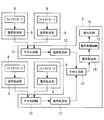
- the solid-state imaging device 1 includes a plurality of color pixels arranged in a Bayer arrangement in two dimensions, and photoelectric conversion that converts light incident on each pixel into an electrical signal.
- Unit 2 an image reading unit (pixel mixing reading unit) 3 that reads out pixel signals composed of electrical signals acquired in photoelectric conversion unit 2, mixes them for the same color, and outputs a multi-channel reduced image signal, and the image
- An inter-channel shift correction unit 4 that corrects a positional shift of the reduced image signal between channels with respect to the reduced image signal output from the reading unit 3, and a tone conversion such as ⁇ correction with respect to the corrected reduced image signal.
- a gradation conversion unit 5 a YC conversion unit (color conversion unit) 6 that separates the reduced image signal output from the gradation conversion unit 5 into a luminance signal and a color difference signal, and the YC conversion unit 6 Reduce the amount of data by thinning out color difference signals And a pixel thinning unit 7 for performing.
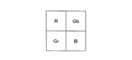
- the photoelectric conversion unit 2 is a two-dimensional array of a set of Bayer-arranged R channel pixels, Gr channel pixels, Gb channel pixels, and B channel pixels, as shown in FIG. It is arranged in an array. As shown in FIG. 4, each pixel includes a photodiode 8 that photoelectrically converts incident light, and a charge transfer unit 9 that transfers charges output from the photodiode 8.
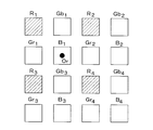
- the image reading unit 3 mixes image signals of pixels of the same color for every 4 ⁇ 4 pixel regions (blocks) 10 of a full resolution Bayer image as shown in FIG. 3 channel (3 plates) reduced image signals are output.
- Each block 10 includes four R channel pixels R 1 , R 2 , R 3 , R 4 , and eight G channel pixels Gr 1 , Gr 2 , Gr 3 , Gr 4 , Gb 1 , Gb 2 , Gb 3. , Gb 4 and four B channel pixels B 1 , B 2 , B 3 , B 4 are included.
- Pixels R 1 of the four R-channel in the block 10 of FIG. 4, R 2, R 3, R 4, corresponds to the photodiode of FIG.
- the image reading unit 3 is provided for every two pixels, and an averaging circuit 11 that averages the charges transferred from the two charge transfer units 9 and a charge transfer unit that transfers the charges averaged by the averaging circuits 11 12, an averaging circuit 13 that is provided for every four pixels, averages the charges transferred from the two charge transfer units 12, and a charge transfer unit 14 that transfers the charges output from the averaging circuit 13.
- the charge signal read by the readout circuit 16 is converted into a voltage signal by a floating diffusion amplifier (not shown), and further converted into a digital image signal by an A / D converter (not shown).
- the inter-channel misalignment correction unit 4 matches the coordinates of the R channel reduced image signal and the B channel reduced image signal mixed and read by the image reading unit 3 with the coordinates of the G channel reduced image signal. It is a position shift correction unit that corrects the position shift. Specifically, as shown in FIG. 5, the four R channel pixels R 1 , R 2 , R 3 , and R 4 in the block 10 of FIG. 3 are located on the upper left side in the same block. Therefore, the mixed output of the pixels R 1 , R 2 , R 3 , and R 4 is output as a reduced image signal having coordinates at the center of gravity position Or. The center-of-gravity position Or in this case, coincides with the second column of the coordinate pixel B 1 from the top in the second column from the left.
- the four B-channel pixels B 1 , B 2 , B 3 , B 4 in the block 10 of FIG. 3 are located on the lower right side in the block. Therefore, the mixed output of the pixels B 1 , B 2 , B 3 , and B 4 is output as a reduced image signal having coordinates at the center of gravity position Ob.
- the center-of-gravity position Ob cases are consistent from below in the second column from the right in the second row of the coordinate pixels R 1.
- the position Og coincides with the center position of the block 10.
- the reduced image signal of the G channel is output as a signal having the center position of the block 10 as coordinates.
- the reduced image signals of the R channel and the B channel are reduced images of the G channel. It has coordinates shifted diagonally up or down by 1 / (2n) pixels with respect to the coordinates of the signal.
- the inter-channel misalignment correction unit 4 corrects this misalignment, and performs four-point interpolation according to the following equation 1 on the reduced image signals of the R channel and the B channel.
- the coordinates (i, j) indicate the coordinates where the G channel pixel exists.
- the four coordinates (ib, jb), (ib, j + a), (i + a, jb), (i + a, j + a) are the nearest R channel to the coordinate (i, j)
- the coordinates where the B channel pixel exists are shown. This operation can be realized using a line memory and some arithmetic operators. Note that the inter-channel misalignment correction unit 4 and subsequent processes are performed on the digital image signal, and are calculated by a logic circuit mounted in the solid-state imaging device 1.
- the gradation conversion unit 5 performs gradation conversion represented by ⁇ correction or the like on each reduced image signal of the input RGB channel, and then reduces the bit accuracy of the image signal somewhat (for example, A / D). The amount of data is reduced by compressing the bit precision after conversion to 8 bits compared to 12 bits).
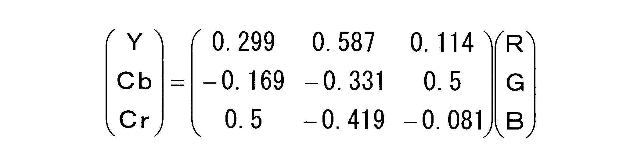
- the YC converter 6 converts the RGB channel image signal after gradation conversion by the gradation converter 5 into a luminance signal (Y) and a color difference signal (Cb / Cr) signal.
- Y luminance signal
- Cb / Cr color difference signal
- the image thinning unit 7 thins out the color difference signal (Cb / Cr) converted by the YC conversion unit 6 at a predetermined interval to reduce the data amount.
- the thinning-out amount is 4: 2: 2 format as shown in FIG. 9A (Y signal is 1 and Cb / Cr signal is 1/2), or 4 as shown in FIG. 9B. : 2: 0 format (Y signal is 1 and Cb / Cr signal is 1/4).
- a circular symbol is a Y signal
- a square symbol is a Cb signal
- a triangular symbol is a Cr signal.
- Table 1 shows the data amount of intermediate output and final output for various reduction ratios when the number of pixels of full resolution is 36 million pixels (36 megapixels).
- bit accuracy at the time of reading is 12 bits and the output of the gradation conversion unit is 8 bits.
- the amount of data output by the solid-state imaging device 1 according to the present embodiment is shown in the D column (in the case of 4: 2; 2 format) or the E column (in the case of 4: 2: 0 format).
- the D column in the case of 4: 2; 2 format
- the E column in the case of 4: 2: 0 format.
- the solid-state imaging device 1 since a multi-channel reduced image signal is output instead of a reduced Bayer image, reproducibility that has conventionally occurred to reconstruct a reduced Bayer image is possible. Therefore, there is an effect that a high-definition image can be reproduced while reducing the data transfer amount without causing a significant frequency band reduction.
- the amount of data output from the gradation conversion unit 5 can be reduced, and the YC conversion unit 6 and the pixel thinning unit 7 thin out color difference signals that are difficult to identify by human vision, thereby changing the image. There is an advantage that the amount of data can be reduced while suppressing.
- the solid-state imaging device 20 according to the present embodiment outputs a reduced three-plate image having a vertical / horizontal size of (1 / odd) from a full-resolution Bayer image. An example will be described.
- the solid-state imaging device 20 includes a gain correction unit (specific channel gain correction unit) 21 instead of the inter-channel shift correction unit 4. This is different from the solid-state imaging device 1 according to the embodiment.
- the gain correction unit 21 multiplies the G-channel reduced image signal by the gain among the reduced image signals mixed and read out by the image reading unit 3.
- the image reading unit 3 mixes image signals of pixels of the same color for every 5 ⁇ 5 pixel regions (blocks) 22 of a full resolution Bayer image as shown in FIGS. 11 (a) to 11 (d).
- a reduced image signal of 3 channels (3 plates) of R, G, and B is output.
- Each block 22 includes 4, 6 or 9 R pixels, 12 or 13 G pixels, and 4, 6 or 9 B pixels.
- the block 22 can take four mixed patterns as shown in FIGS. 11 (a) to 11 (d) depending on the cutout method.
- the center-of-gravity positions of the R channel pixel, the G channel pixel, and the B channel pixel in each mixed pattern coincide with the center positions of the 5 ⁇ 5 blocks 22 in any case. Therefore, it is not necessary to correct the displacement of the center of gravity position as in the first embodiment.
- the number of Gr pixels that are G channel pixels in the RG column differs from the number of Gb pixels that are G channel pixels in the BG column. ing.
- the mixed patterns of FIGS. 11A and 11C include 6 Gr pixels and 6 Gb pixels, and the mixed pattern of FIG. 11B includes 4 Gr images and 9 Gb pixels. In the mixed pattern (d), 9 Gr pixels and 4 Gb pixels are included.
- the green filter of the RG column Gr pixel and the Gb pixel of the BG column are mainly used. It is known that there is a case where a difference occurs between an image signal obtained from a Gr pixel and an image signal obtained from a Gb pixel.
- the gain correction unit calculates the correction gain from the number of Gr pixels and Gb pixels and the count based on the difference in spectral characteristics, and the reduced image signal and Gb read from the Gr pixel.
- the reduced image signals read from the pixels are multiplied by different correction gains. Thereby, generation
- the solid-state imaging device 1 it is possible to suppress the noise by correcting the shift of the reduced image signal between channels, and as shown in Table 1, the same amount as the data amount of the reduced Bayer image.
- the position correction unit or the gain correction unit as the inter-channel shift correction unit has been described.
- the number of pixels of the block to be selected is an even number.
- the position correction unit or the gain correction unit may be selected and applied depending on whether it is an odd number or an odd number.
- the photoelectric conversion unit in which pixels of a plurality of colors are arranged in a Bayer is illustrated, but the present invention is not limited to this, and pixels of a plurality of colors having a predetermined periodicity in the color array are arranged vertically and horizontally.
- the present invention can be applied to a case where an arbitrary photoelectric conversion unit arranged two-dimensionally is provided.
- the cases of the reduction magnifications 1/4 and 1/5 have been illustrated, instead of this, the present invention may be applied to any reduction magnifications of 1 / even and 1 / odd.
Landscapes
- Engineering & Computer Science (AREA)
- Multimedia (AREA)
- Signal Processing (AREA)
- Physics & Mathematics (AREA)
- General Physics & Mathematics (AREA)
- Theoretical Computer Science (AREA)
- Spectroscopy & Molecular Physics (AREA)
- Color Television Image Signal Generators (AREA)
- Image Processing (AREA)
Abstract
本来再現可能な周波数帯域の削減を最小限に抑えて、原画像を縮小処理する。色配列に所定の周期性を有する複数色の画素を縦横に2次元的に配列してなる光電変換部(2)と、該光電変換部(2)によって取得された画素信号を、n×n(nは2以上の任意の整数)個のブロック内の同色の画素ごとに混合し、縮小率1/nの多チャネルの縮小画像信号を出力する画素混合読出部(3)と、該画素混合読出部(3)により出力されたチャネル間の縮小画像信号のズレを補正して出力するチャネル間ズレ補正部(4)を備える固体撮像素子(1)である。
Description
本発明は、固体撮像素子に関するものである。
従来、所定の色配列(ベイヤ配列が一般的であるため、以下、ベイヤ配列とも言う。)を有する原画像の画素データに対し、ライン単位でフィルタ処理を行うことにより輝度データと色差データとの2系統のデータを抽出し、抽出された輝度データおよび色差データにそれぞれ独立に帯域制限フィルタを適用してリサイズを行った後に、元のベイヤ配列を再現するように再構成する固体撮像素子が知られている(例えば、特許文献1参照。)。この固体撮像素子によれば、上記処理により、モアレや偽色等の偽信号を低減しながら解像感を保持することとしている。
しかしながら、特許文献1の固体撮像素子では、リサイズ後にベイヤ配列に再構成するので、本来再現可能な周波数帯域まで削減されてしまう不都合がある。
図12に、フル解像度のベイヤ画像と、縦横とも1/2に縮小した縮小ベイヤ画像の限界帯域を2次元の空間周波数座標系に表したものを示す。ここで、fsはフル解像度画像の画素ピッチ(サンプリング周期)に対応するナイキスト周波数を示している。
図12に、フル解像度のベイヤ画像と、縦横とも1/2に縮小した縮小ベイヤ画像の限界帯域を2次元の空間周波数座標系に表したものを示す。ここで、fsはフル解像度画像の画素ピッチ(サンプリング周期)に対応するナイキスト周波数を示している。
図12によれば、ベイヤ配列におけるG信号の再現帯域は、垂直および水平方向に比べて斜め45°方向の再現帯域が低い菱形となり、斜め45°方向の再現帯域が削減されてしまっている。さらに、R/B信号の再現帯域は、斜め45°方向についてはG信号と同じであるが、垂直および水平方向の再現帯域はG信号の半分となり、G信号と比較しても、本来再現可能な周波数帯域が大幅に削減されてしまっている。
本発明は、上述した事情に鑑みてなされたものであって、本来再現可能な周波数帯域の削減を最小限に抑えて、縮小されたフルカラーの多チャネル信号を得ることができる固体撮像素子を提供することを目的としている。
上記目的を達成するために、本発明は以下の手段を提供する。
本発明の一態様は、色配列に所定の周期性を有する複数色の画素を縦横に2次元的に配列してなる光電変換部と、該光電変換部によって取得された画素信号を、n×n(nは2以上の任意の整数)個のブロック内の同色の画素ごとに混合し、縮小率1/nの多チャネルの縮小画像信号を出力する画素混合読出部と、該画素混合読出部により出力されたチャネル間の縮小画像信号のズレを補正して出力するチャネル間ズレ補正部とを備える固体撮像素子である。
本発明の一態様は、色配列に所定の周期性を有する複数色の画素を縦横に2次元的に配列してなる光電変換部と、該光電変換部によって取得された画素信号を、n×n(nは2以上の任意の整数)個のブロック内の同色の画素ごとに混合し、縮小率1/nの多チャネルの縮小画像信号を出力する画素混合読出部と、該画素混合読出部により出力されたチャネル間の縮小画像信号のズレを補正して出力するチャネル間ズレ補正部とを備える固体撮像素子である。
本態様によれば、光電変換部に入射した被写体からの光が、周期的に色配列された画素毎に光電変換されて電気的な画像信号に変換され、取得された画像信号がn×n個のブロック内の同色の画素ごとに画素混合読出部において混合され、縮小率1/nの多チャネルの縮小画像信号が出力される。色ごとに混合された多チャネルの縮小画像信号は、画素の色配列に応じたズレを含んでいるので、チャネル間ズレ補正部により補正することで、ズレのない多チャネルの縮小画像信号を出力することができる。縮小ベイヤ画像ではなく、多チャネルの縮小画像信号を出力するので、従来、縮小ベイヤ画像に再構成するために生じていた再現可能な周波数帯域の削減が発生せず、データ転送量を削減しつつ高精細な画像を再現することができる。
上記態様においては、前記光電変換部が、前記画素をベイヤ配列してなり、前記画素混合読出部が、混合された同色の画素信号を前記ブロック内の同色の画素の重心位置に配置される座標の縮小画像信号として算出し、前記チャネル間ズレ補正部は、nが偶数である場合に、各色の縮小画像信号の座標を一致させるように縮小画像信号の位置ズレを補正する位置ズレ補正部を備えていてもよい。
ベイヤ配列された光電変換部の各画素により取得される画像信号は画素混合読出部により混合されるブロックが偶数の画素を含む場合に、ブロック内の同色の画素の重心位置が色間でずれることになる。本態様によれば、チャネル間ズレ補正部の位置ズレ補正部により、位置ズレを補正して座標を一致させた多チャネルの縮小画像信号を出力することができる。
また、上記態様においては、前記光電変換部が、前記画素をベイヤ配列してなり、前記チャネル間ズレ補正部は、nが奇数である場合に、隣接する行間における同色の画素の特性の差を補正するゲイン補正部を備えていてもよい。
ベイヤ配列された光電変換部の各画素により取得される画像信号は、画素混合読出部により混合されるブロックが奇数の画素を含む場合に、ブロック内の同色の画素の重心位置の色間での位置ズレは生じないが、2種類のGチャネルにおけるフィルタの分光特性の相違によりずれることになる。本態様によれば、チャネル間ズレ補正部のゲイン補正部により、フィルタの分光特性のずれを補正してノイズの少ない多チャネルの縮小画像信号を出力することができる。
また、上記態様においては、前記光電変換部が、前記画素をベイヤ配列してなり、前記画素混合読出部が、混合された同色の画素信号を前記ブロック内の同色の画素の重心位置に配置される座標の縮小画像信号として算出し、前記チャネル間ズレ補正部は、nが偶数である場合に、各色の縮小画像信号の座標を一致させるように縮小画像信号の位置ズレを補正する位置ズレ補正部と、nが奇数である場合に、隣接する行間における同色の画素の特性の差を補正するゲイン補正部とを備えていてもよい。
このようにすることで、画素混合読出部により混合されるブロックの画素数が偶数であっても奇数であってもチャネル間ズレ補正部によりチャネル間の縮小画像信号のズレを補正して出力することができる。
また、上記態様においては、前記チャネル間ズレ補正部により補正された多チャネルの縮小画像信号を、輝度信号と色差信号とに分離し、色差信号の信号帯域を制限する色変換部と、該色変換部から出力された色差信号を間引く画素間引部とを備えていてもよい。
このようにすることで、人の視覚によって識別しにくい色差信号を間引くので、画像上の変化を抑えつつデータ量を削減することができる。
このようにすることで、人の視覚によって識別しにくい色差信号を間引くので、画像上の変化を抑えつつデータ量を削減することができる。
また、上記態様においては、前記チャネル間ズレ補正部により補正された多チャネルの縮小画像信号に対して階調変換を行い、AD変換後のビット幅より小さいビット幅で表現される画像信号として出力する階調変換部を備えていてもよい。
このようにすることで、階調変換部から出力されるデータ量を削減することができる。
このようにすることで、階調変換部から出力されるデータ量を削減することができる。
また、本発明の他の態様は、色配列に所定の周期性を有する複数色の画素を縦横に2次元的に配列してなる光電変換部によって取得された画素信号を、n×n(nは2以上の任意の整数)個のブロック内の同色の画素毎に混合し、縮小率1/nの多チャネルの縮小画像信号を出力する画素混合読出部と、該画素混合読出部により出力されたチャネル間の縮小画像信号のズレを補正して出力するチャネル間ズレ補正部とを備える固体撮像素子である。
本発明によれば、本来再現可能な周波数帯域の削減を最小限に抑えて、縮小されたフルカラーの多チャネル信号を得ることができるという効果を奏する。
本発明の第1の実施形態に係る固体撮像素子1について、図面を参照して以下に説明する。
本実施形態に係る固体撮像素子1は、フル解像度ベイヤ画像信号から縦横サイズが(1/偶数)となる縮小3板化画像信号を生成するものであり、ここでは、縦横1/4縮小するものとして説明する。一般には縦横1/n縮小した画像の実際のサイズは1/n2となるが、本実施形態の説明においては、特に追記がない限り、1/n縮小とは縦横サイズを1/n縮小することを意味するものとする。
本実施形態に係る固体撮像素子1は、フル解像度ベイヤ画像信号から縦横サイズが(1/偶数)となる縮小3板化画像信号を生成するものであり、ここでは、縦横1/4縮小するものとして説明する。一般には縦横1/n縮小した画像の実際のサイズは1/n2となるが、本実施形態の説明においては、特に追記がない限り、1/n縮小とは縦横サイズを1/n縮小することを意味するものとする。
本実施形態に係る固体撮像素子1は、図1に示されるように、ベイヤ配列された複数色の画素が縦横2次元に配列され、各画素に入射された光を電気信号に変換する光電変換部2と、該光電変換部2において取得された電気信号からなる画素信号を読み出して同色毎に混合し多チャネルの縮小画像信号を出力する画像読出部(画素混合読出部)3と、該画像読出部3から出力された縮小画像信号に対し、チャネル間の縮小画像信号の位置ズレを補正するチャネル間ズレ補正部4と、補正された縮小画像信号に対しγ補正等の階調変換を行う階調変換部5と、該階調変換部5から出力された縮小画像信号を輝度信号と色差信号とに分離するYC変換部(色変換部)6と、該YC変換部6において変換された色差信号を間引いてデータ量の削減を行う画素間引部7とを備えている。
光電変換部2は、図2に示されるように、ベイヤ配列されたRチャネルの画素,Grチャネルの画素,Gbチャネルの画素,Bチャネルの画素の集合を図3に示されるように、2次元的に配列して構成されている。各画素は、図4に示されるように、入射光を光電変換するフォトダイオード8、フォトダイオード8から出力された電荷を転送する電荷転送部9を備えている。
画像読出部3は、例えば、図3に示されるようなフル解像度のベイヤ画像の4×4個の画素領域(ブロック)10毎に、同色の画素の画像信号を混合し、R,G,Bの3チャネル(3板)の縮小画像信号を出力するようになっている。各ブロック10には4個のRチャネル画素R1,R2,R3,R4、8個のGチャネルの画素Gr1,Gr2,Gr3,Gr4,Gb1,Gb2,Gb3,Gb4および4個のBチャネルの画素B1,B2,B3,B4が含まれている。
ここでは、4個のRチャネルの画素R1,R2,R3,R4からの画像信号の混合を例に挙げて説明する。図4のブロック10中の4個のRチャネルの画素R1,R2,R3,R4が、図4のフォトダイオードに対応している。画像読出部3は、2画素ごとに設けられて2つの電荷転送部9から転送されてきた電荷を平均する平均化回路11と、各平均化回路11によって平均された電荷を転送する電荷転送部12と、4画素ごとに設けられ、2つの電荷転送部12から転送されてきた電荷を平均化する平均化回路13と、該平均化回路13から出力された電荷を転送する電荷転送部14と、該電荷転送部14により転送されてきた電荷を蓄積する電荷蓄積回路15と、該電荷蓄積回路15から電荷信号を読み出す読出回路16とを備えている。
読出回路16により読み出された電荷信号はフローティングディフュージョンアンプ(図示略)にて電圧信号に変換され,さらにA/D変換器(図示略)によってデジタル画像信号に変換されるようになっている。
チャネル間ズレ補正部4は、画像読出部3により混合されて読み出されたRチャネルの縮小画像信号およびBチャネルの縮小画像信号の座標を、Gチャネルの縮小画像信号の座標に一致させるように位置ズレを補正する位置ズレ補正部である。
具体的には、図5に示されるように、図3のブロック10の中の4個のRチャネルの画素R1,R2,R3,R4は同ブロックの中で左上側に位置しているため、それらの画素R1,R2,R3,R4の混合出力はそれらの重心位置Orに座標を有する縮小画像信号として出力される。この場合の重心位置Orは、左から2列目で上から2列目の画素B1の座標に一致している。
具体的には、図5に示されるように、図3のブロック10の中の4個のRチャネルの画素R1,R2,R3,R4は同ブロックの中で左上側に位置しているため、それらの画素R1,R2,R3,R4の混合出力はそれらの重心位置Orに座標を有する縮小画像信号として出力される。この場合の重心位置Orは、左から2列目で上から2列目の画素B1の座標に一致している。
また、図7に示されるように、図3のブロック10の中の4個のBチャネルの画素B1,B2,B3,B4は同ブロックの中で右下側に位置しているため、それらの画素B1,B2,B3,B4の混合出力はそれらの重心位置Obに座標を有する縮小画像信号として出力される。この場合の重心位置Obは、右から2列目で下から2列目の画素R1の座標に一致している。
一方、図6に示されるように、図4のブロック10の中の8個のGチャネルの画素Gr1,Gr2,Gr3,Gr4,Gb1,Gb2,Gb3,Gb4の重心位置Ogは、ブロック10の中心位置に一致している。
一方、図6に示されるように、図4のブロック10の中の8個のGチャネルの画素Gr1,Gr2,Gr3,Gr4,Gb1,Gb2,Gb3,Gb4の重心位置Ogは、ブロック10の中心位置に一致している。
したがって、Gチャネルの縮小画像信号は、ブロック10の中心位置を座標とする信号として出力されるが、図8に示されるように、RチャネルおよびBチャネルの縮小画像信号は、Gチャネルの縮小画像信号の座標に対して1/(2n)画素分斜め上または斜め下にずれた座標を有している。
チャネル間ズレ補正部4は、この位置ズレを補正するものであり、RチャネルおよびBチャネルの縮小画像信号に対して以下の数1による4点補間を行うようになっている。
チャネル間ズレ補正部4は、この位置ズレを補正するものであり、RチャネルおよびBチャネルの縮小画像信号に対して以下の数1による4点補間を行うようになっている。
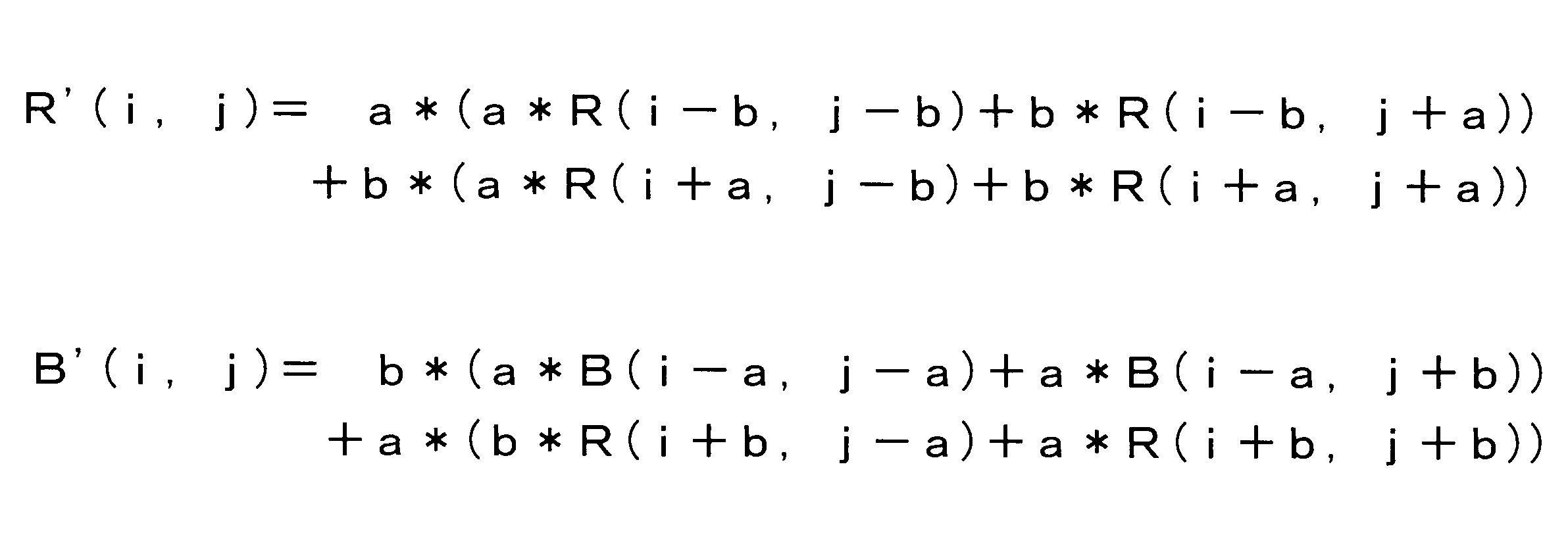
数1において、座標(i,j)はGチャネルの画素が存在する座標を示している。4点の座標(i-b,j-b)、(i-b,j+a)、(i+a,j-b)、(i+a,j+a)は座標(i,j)に対して最近傍のRチャネルまたはBチャネルの画素が存在する座標を示している。この演算はラインメモリといくつかの算術演算器を用いて実現可能である。
なお、チャネル間ズレ補正部4以降は、デジタル画像信号に対する処理となり、固体撮像素子1内に搭載された論理回路にて演算されるようになっている。
なお、チャネル間ズレ補正部4以降は、デジタル画像信号に対する処理となり、固体撮像素子1内に搭載された論理回路にて演算されるようになっている。
階調変換部5は、入力されたRGBチャネルの各縮小画像信号に対してγ補正等に代表される階調変換を行い、その後に画像信号のビット精度をいくらか削減する(例えば、A/D変換後のビット精度が12ビットであるのに対して8ビットに圧縮する等)ことにより、データ量を削減するようになっている。
YC変換部6は階調変換部5による階調変換後のRGBチャネルの画像信号を輝度信号(Y)と色差信号(Cb/Cr)信号に変換するようになっている。ITU-R BT.601方式による一般的な変換式は数2に示す通りである。
画像間引部7は、YC変換部6により変換された色差信号(Cb/Cr)を所定の間隔で間引き、データ量の削減を行うようになっている。間引き量は、図9(a)に示されるような4:2:2フォーマット(Y信号が1に対してCb/Cr信号が1/2)や、図9(b)に示されるような4:2:0フォーマット(Y信号が1に対してCb/Cr信号が1/4)等が代表的なものである。図中、円形の記号はY信号、四角形の記号はCb信号、三角形の記号はCr信号である。
表1は、フル解像度の画素数を仮に3600万画素(36メガピクセル)とした場合の、各種縮小率に対する中間出力および最終出力のデータ量を示したものである。ここで、読み出し時のビット精度を12ビット、階調変換部の出力を8ビットと仮定した。
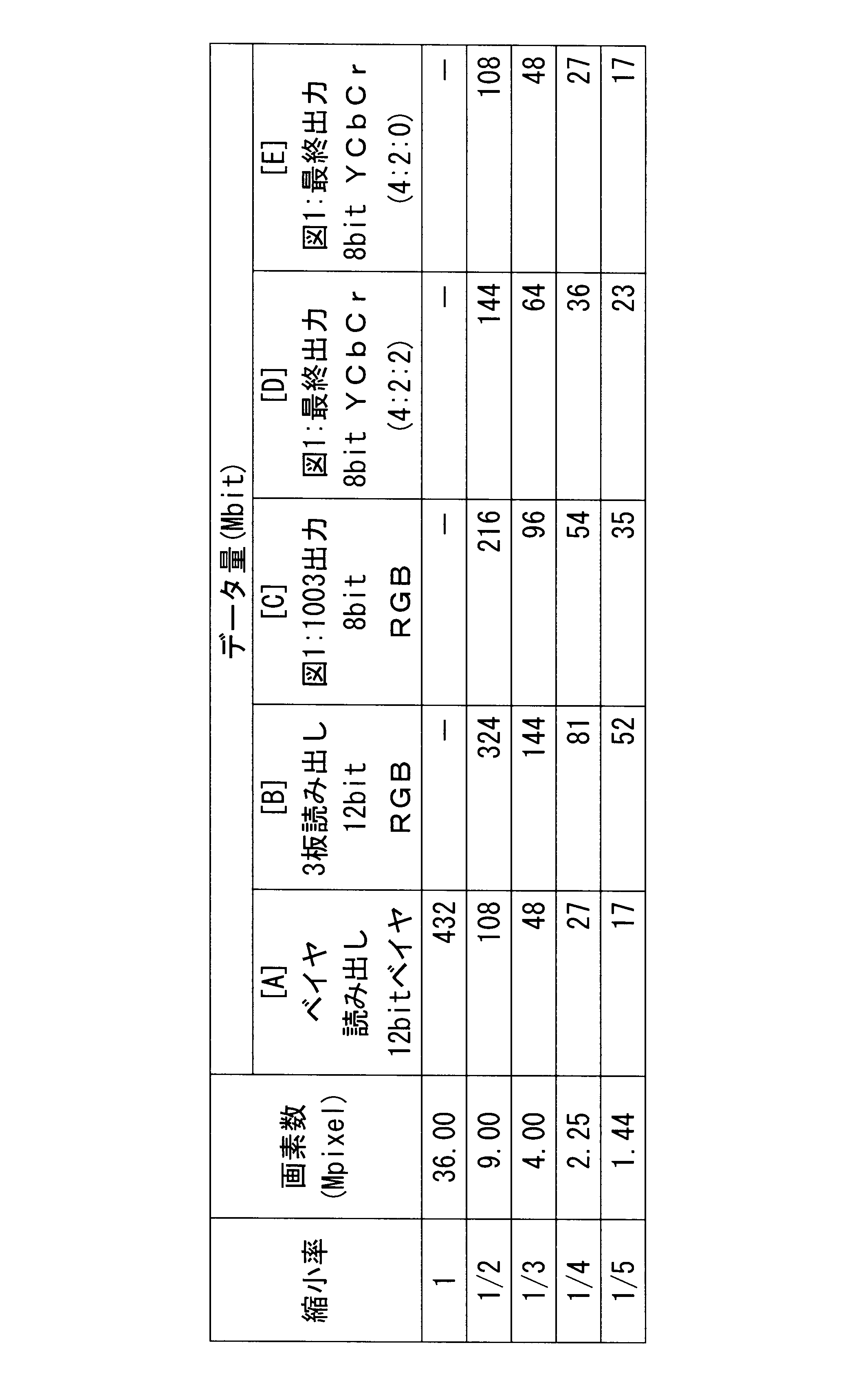
これによれば、本実施形態に係る固体撮像素子1により出力されるデータ量はD列(4:2;2フォーマットの場合)、もしくはE列(4:2:0フォーマットの場合)に示すものとなり、縮小ベイヤ画像のデータ量(A列)と同程度で高解像の3板化画像信号を転送することができることが分かる。
このように、本実施形態に係る固体撮像素子1によれば、縮小ベイヤ画像ではなく、多チャネルの縮小画像信号を出力するので、従来、縮小ベイヤ画像に再構成するために生じていた再現可能な周波数帯域の削減が発生せず、データ転送量を削減しつつ高精細な画像を再現することができるという効果を奏する。また、階調変換部5から出力されるデータ量を削減することができるとともに、YC変換部6および画素間引部7により、人の視覚によって識別しにくい色差信号を間引いて、画像上の変化を抑えつつデータ量を削減することができるという利点がある。
次に、本発明の第2の実施形態に係る固体撮像素子20について、図面を参照して以下に説明する。
本実施形態の説明において、上述した第1の実施形態に係る固体撮像素子1と構成を共通とする箇所には同一符号を付して説明を省略する。
本実施形態に係る固体撮像素子20は、フル解像度のベイヤ画像から縦横サイズが(1/奇数)となる縮小3板化画像を出力するものであり、以降は基本的に縦横を1/5縮小するものを例示して説明する。
本実施形態の説明において、上述した第1の実施形態に係る固体撮像素子1と構成を共通とする箇所には同一符号を付して説明を省略する。
本実施形態に係る固体撮像素子20は、フル解像度のベイヤ画像から縦横サイズが(1/奇数)となる縮小3板化画像を出力するものであり、以降は基本的に縦横を1/5縮小するものを例示して説明する。
図10に示されるように、本実施形態に係る固体撮像素子20は、チャネル間ズレ補正部4に代えて、ゲイン補正部(特定チャネルゲイン補正部)21を有している点で、第1の実施形態に係る固体撮像素子1と相違している。
このゲイン補正部21は、画像読出部3により混合読み出しされた縮小画像信号の内、Gチャネルの縮小画像信号にゲインを乗算するものである。
このゲイン補正部21は、画像読出部3により混合読み出しされた縮小画像信号の内、Gチャネルの縮小画像信号にゲインを乗算するものである。
画像読出部3は、例えば、図11(a)~(d)に示されるようなフル解像度のベイヤ画像の5×5個の画素領域(ブロック)22毎に、同色の画素の画像信号を混合し、R,G,Bの3チャネル(3板)の縮小画像信号を出力するようになっている。各ブロック22には4個、6個または9個のR画素、12個または13個のG画素、および4個、6個または9個のB画素が含まれている。そして、ブロック22は、その切り出し方によって、図11(a)~(d)に示されるように、4つの混合パターンをとることができる。
本実施形態の場合には、各混合パターンにおけるRチャネルの画素、Gチャネルの画素およびBチャネルの画素の重心位置は、いずれの場合においても、5×5個のブロック22の中心位置に一致しているので、第1の実施形態のように重心位置の位置ズレを補正する必要はない。しかしながら、各混合パターンにおいて縮小画像信号を構成するためのGチャネルにおいて、R-G列のGチャネルの画素であるGr画素と、B-G列のGチャネルの画素であるGb画素の個数が異なっている。
すなわち、図11(a)、(c)の混合パターンでは、6個のGr画素と6個のGb画素を含み、(b)の混合パターンでは、4個のGr画像と9個のGb画素を含み、(d)の混合パターンでは、9個のGr画素と4個のGb画素を含んでいる。
一般的なベイヤ配列の固体撮像素子においては、明るさと色成分が一様な被写体を撮像した場合であっても、主にR-G列のGr画素の緑色フィルタとB-G列のGb画素の緑色フィルタとは分光特性が異なっており、Gr画素から得られる画像信号とGb画素から得られる画像信号との間に差が生じる場合があることが知られている。
そこで、本実施形態においては、ゲイン補正部により、Gr画素とGb画素のそれぞれの個数と分光特性の相違に基づく計数とから補正ゲインを計算しておき、Gr画素から読み取った縮小画像信号およびGb画素から読み取った縮小画像信号に対して、それぞれ異なる補正ゲインを乗算することとしている。
これにより、緑色フィルタの分光特性が異なることによる格子状または縞状のノイズの発生を抑制することができる。
これにより、緑色フィルタの分光特性が異なることによる格子状または縞状のノイズの発生を抑制することができる。
すなわち、本実施形態に係る固体撮像素子1においても、チャネル間の縮小画像信号のズレを補正してノイズを抑制することができ、表1に示されるように、縮小ベイヤ画像のデータ量と同程度のデータ量で、高解像度の画像を再現可能な縮小3板化画像信号を出力することができるという利点がある。
なお、上記実施形態においては、チャネル間ズレ補正部として、位置補正部またはゲイン補正部のいずれかを有する場合について説明したが、これに代えて、両者を備え、選択するブロックの画素数が偶数か奇数かによって位置補正部またはゲイン補正部を選択して適用することにしてもよい。
また、本実施形態においては、複数色の画素がベイヤ配列された光電変換部について例示したが、これに限定されるものではなく、色配列に所定の周期性を有する複数色の画素を縦横に2次元的に配列してなる任意の光電変換部を有する場合に適用することができる。
また、縮小倍率1/4と1/5の場合を例示したが、これに代えて、任意の1/偶数および1/奇数の縮小倍率の場合に適用してもよい。
また、縮小倍率1/4と1/5の場合を例示したが、これに代えて、任意の1/偶数および1/奇数の縮小倍率の場合に適用してもよい。
1,20 固体撮像素子
2 光電変換部
3 画素混合読出部(画像読出部)
4 位置補正部(チャネル間ズレ補正部)
5 階調変換部
6 YC変換部(色変換部)
7 画素間引部
10,22 ブロック
21 ゲイン補正部(チャネル間ズレ補正部)
2 光電変換部
3 画素混合読出部(画像読出部)
4 位置補正部(チャネル間ズレ補正部)
5 階調変換部
6 YC変換部(色変換部)
7 画素間引部
10,22 ブロック
21 ゲイン補正部(チャネル間ズレ補正部)
Claims (7)
- 色配列に所定の周期性を有する複数色の画素を縦横に2次元的に配列してなる光電変換部と、
該光電変換部によって取得された画素信号を、n×n(nは2以上の任意の整数)個のブロック内の同色の画素毎に混合し、縮小率1/nの多チャネルの縮小画像信号を出力する画素混合読出部と、
該画素混合読出部により出力されたチャネル間の縮小画像信号のズレを補正して出力するチャネル間ズレ補正部とを備える固体撮像素子。 - 前記光電変換部が、前記画素をベイヤ配列してなり、
前記画素混合読出部が、混合された同色の画素信号を前記ブロック内の同色の画素の重心位置に配置される座標の縮小画像信号として算出し、
前記チャネル間ズレ補正部は、nが偶数である場合に、各色の縮小画像信号の座標を一致させるように縮小画像信号の位置ズレを補正する位置ズレ補正部を備える請求項1に記載の固体撮像素子。 - 前記光電変換部が、前記画素をベイヤ配列してなり、
前記チャネル間ズレ補正部は、nが奇数である場合に、隣接する行間における同色の画素の特性の差を補正するゲイン補正部を備える請求項1に記載の固体撮像素子。 - 前記光電変換部が、前記画素をベイヤ配列してなり、
前記画素混合読出部が、混合された同色の画素信号を前記ブロック内の同色の画素の重心位置に配置される座標の縮小画像信号として算出し、
前記チャネル間ズレ補正部は、nが偶数である場合に、各色の縮小画像信号の座標を一致させるように縮小画像信号の位置ズレを補正する位置ズレ補正部と、nが奇数である場合に、隣接する行間における同色の画素の特性の差を補正するゲイン補正部とを備える請求項1に記載の固体撮像素子。 - 前記チャネル間ズレ補正部により補正された多チャネルの縮小画像信号を、輝度信号と色差信号とに分離し、色差信号の信号帯域を制限する色変換部と、該色変換部から出力された色差信号を間引く画素間引部とを備える請求項1から請求項4のいずれかに記載の固体撮像素子。
- 前記チャネル間ズレ補正部により補正された多チャネルの縮小画像信号に対して階調変換を行い、AD変換後のビット幅より小さいビット幅で表現される画像信号として出力する階調変換部を備える請求項1から請求項5のいずれかに記載の固体撮像素子。
- 色配列に所定の周期性を有する複数色の画素を縦横に2次元的に配列してなる光電変換部によって取得された画素信号を、n×n(nは2以上の任意の整数)個のブロック内の同色の画素毎に混合し、縮小率1/nの多チャネルの縮小画像信号を出力する画素混合読出部と、
該画素混合読出部により出力されたチャネル間の縮小画像信号のズレを補正して出力するチャネル間ズレ補正部とを備える固体撮像素子。
Priority Applications (1)
| Application Number | Priority Date | Filing Date | Title |
|---|---|---|---|
| US15/208,014 US9877005B2 (en) | 2014-03-13 | 2016-07-12 | Solid-state image-capturing device which reduces number of signal channels |
Applications Claiming Priority (2)
| Application Number | Priority Date | Filing Date | Title |
|---|---|---|---|
| JP2014-050420 | 2014-03-13 | ||
| JP2014050420A JP6396044B2 (ja) | 2014-03-13 | 2014-03-13 | 固体撮像素子 |
Related Child Applications (1)
| Application Number | Title | Priority Date | Filing Date |
|---|---|---|---|
| US15/208,014 Continuation US9877005B2 (en) | 2014-03-13 | 2016-07-12 | Solid-state image-capturing device which reduces number of signal channels |
Publications (1)
| Publication Number | Publication Date |
|---|---|
| WO2015137144A1 true WO2015137144A1 (ja) | 2015-09-17 |
Family
ID=54071592
Family Applications (1)
| Application Number | Title | Priority Date | Filing Date |
|---|---|---|---|
| PCT/JP2015/055723 Ceased WO2015137144A1 (ja) | 2014-03-13 | 2015-02-26 | 固体撮像素子 |
Country Status (3)
| Country | Link |
|---|---|
| US (1) | US9877005B2 (ja) |
| JP (1) | JP6396044B2 (ja) |
| WO (1) | WO2015137144A1 (ja) |
Families Citing this family (4)
| Publication number | Priority date | Publication date | Assignee | Title |
|---|---|---|---|---|
| JP6817789B2 (ja) * | 2016-06-10 | 2021-01-20 | ラピスセミコンダクタ株式会社 | 表示ドライバ及び半導体装置 |
| US11128843B2 (en) * | 2020-01-13 | 2021-09-21 | Facebook Technologies, Llc | Image-sensor data compression |
| KR102713585B1 (ko) | 2020-06-30 | 2024-10-07 | 삼성전자주식회사 | 이미지 센서를 포함하는 전자 장치 |
| CN115096555B (zh) * | 2022-06-30 | 2025-04-22 | 湘能华磊光电股份有限公司 | 一种led多针测试机通道亮度差异的修正方法 |
Citations (3)
| Publication number | Priority date | Publication date | Assignee | Title |
|---|---|---|---|---|
| JP2007006038A (ja) * | 2005-06-22 | 2007-01-11 | Canon Inc | 画像処理装置及び画像処理方法及びプログラム及び記憶媒体 |
| JP2007158509A (ja) * | 2005-12-01 | 2007-06-21 | Canon Inc | 撮像装置及び画像処理方法及びプログラム及び記憶媒体 |
| JP2008199177A (ja) * | 2007-02-09 | 2008-08-28 | Olympus Imaging Corp | 画像処理装置およびその方法と電子カメラ |
Family Cites Families (2)
| Publication number | Priority date | Publication date | Assignee | Title |
|---|---|---|---|---|
| JP5280448B2 (ja) | 2008-08-04 | 2013-09-04 | パナソニック株式会社 | 画像処理装置、画像処理方法、画像処理プログラム及び半導体集積回路 |
| US9332239B2 (en) * | 2012-05-31 | 2016-05-03 | Apple Inc. | Systems and methods for RGB image processing |
-
2014
- 2014-03-13 JP JP2014050420A patent/JP6396044B2/ja active Active
-
2015
- 2015-02-26 WO PCT/JP2015/055723 patent/WO2015137144A1/ja not_active Ceased
-
2016
- 2016-07-12 US US15/208,014 patent/US9877005B2/en not_active Expired - Fee Related
Patent Citations (3)
| Publication number | Priority date | Publication date | Assignee | Title |
|---|---|---|---|---|
| JP2007006038A (ja) * | 2005-06-22 | 2007-01-11 | Canon Inc | 画像処理装置及び画像処理方法及びプログラム及び記憶媒体 |
| JP2007158509A (ja) * | 2005-12-01 | 2007-06-21 | Canon Inc | 撮像装置及び画像処理方法及びプログラム及び記憶媒体 |
| JP2008199177A (ja) * | 2007-02-09 | 2008-08-28 | Olympus Imaging Corp | 画像処理装置およびその方法と電子カメラ |
Also Published As
| Publication number | Publication date |
|---|---|
| US9877005B2 (en) | 2018-01-23 |
| JP2015177243A (ja) | 2015-10-05 |
| US20160323555A1 (en) | 2016-11-03 |
| JP6396044B2 (ja) | 2018-09-26 |
Similar Documents
| Publication | Publication Date | Title |
|---|---|---|
| JP4662883B2 (ja) | 二次元カラー固体撮像素子 | |
| JP4377428B2 (ja) | 固体撮像素子及びそれを用いた撮像装置 | |
| US7929807B2 (en) | Colour binning of a digital image to reduce the image resolution | |
| US8023018B2 (en) | Drive method for solid-state imaging device, solid-state imaging device, and imaging apparatus | |
| JP5589146B2 (ja) | 撮像素子及び撮像装置 | |
| JP5054856B1 (ja) | カラー撮像素子 | |
| US9188480B2 (en) | Color filter array and image sensor | |
| US8743246B2 (en) | Color imaging device | |
| CN104025583B (zh) | 图像处理装置、方法及摄像装置 | |
| JPWO2013099637A1 (ja) | カラー撮像素子及び撮像装置 | |
| JP6396044B2 (ja) | 固体撮像素子 | |
| US8922684B2 (en) | Imaging device, control method for imaging device, and storage medium storing a control program for imaging device | |
| CN100444620C (zh) | 固态成像装置驱动方法、固态成像装置以及成像设备 | |
| JP6535454B2 (ja) | 二板式カラーまたは白黒撮像装置と二板式カラーまたは白黒撮像装置の画像処理方法 | |
| US20130038772A1 (en) | Image processing apparatus and image processing method | |
| JP4253095B2 (ja) | 画像データ・フィルタリング装置および方法 | |
| JP2006211631A (ja) | 固体撮像装置および撮像装置 | |
| JP5697418B2 (ja) | 画像処理装置及びその制御方法 | |
| JPWO2020059069A1 (ja) | 二板式撮像装置と二板式撮像装置の画像処理方法とその固体撮像素子の位置決め方法 | |
| JP2009010923A (ja) | デジタル画像のカラービニング | |
| JP6083678B2 (ja) | 画像処理装置 |
Legal Events
| Date | Code | Title | Description |
|---|---|---|---|
| 121 | Ep: the epo has been informed by wipo that ep was designated in this application |
Ref document number: 15762157 Country of ref document: EP Kind code of ref document: A1 |
|
| NENP | Non-entry into the national phase |
Ref country code: DE |
|
| 122 | Ep: pct application non-entry in european phase |
Ref document number: 15762157 Country of ref document: EP Kind code of ref document: A1 |