WO2015129766A1 - アンテナ装置および携帯端末装置 - Google Patents
アンテナ装置および携帯端末装置 Download PDFInfo
- Publication number
- WO2015129766A1 WO2015129766A1 PCT/JP2015/055474 JP2015055474W WO2015129766A1 WO 2015129766 A1 WO2015129766 A1 WO 2015129766A1 JP 2015055474 W JP2015055474 W JP 2015055474W WO 2015129766 A1 WO2015129766 A1 WO 2015129766A1
- Authority
- WO
- WIPO (PCT)
- Prior art keywords
- antenna
- plane
- antenna pattern
- rib
- width
- Prior art date
- Legal status (The legal status is an assumption and is not a legal conclusion. Google has not performed a legal analysis and makes no representation as to the accuracy of the status listed.)
- Ceased
Links
Images




Classifications
-
- G—PHYSICS
- G06—COMPUTING OR CALCULATING; COUNTING
- G06K—GRAPHICAL DATA READING; PRESENTATION OF DATA; RECORD CARRIERS; HANDLING RECORD CARRIERS
- G06K19/00—Record carriers for use with machines and with at least a part designed to carry digital markings
- G06K19/06—Record carriers for use with machines and with at least a part designed to carry digital markings characterised by the kind of the digital marking, e.g. shape, nature, code
- G06K19/067—Record carriers with conductive marks, printed circuits or semiconductor circuit elements, e.g. credit or identity cards also with resonating or responding marks without active components
- G06K19/07—Record carriers with conductive marks, printed circuits or semiconductor circuit elements, e.g. credit or identity cards also with resonating or responding marks without active components with integrated circuit chips
- G06K19/077—Constructional details, e.g. mounting of circuits in the carrier
- G06K19/07749—Constructional details, e.g. mounting of circuits in the carrier the record carrier being capable of non-contact communication, e.g. constructional details of the antenna of a non-contact smart card
- G06K19/07773—Antenna details
- G06K19/07777—Antenna details the antenna being of the inductive type
- G06K19/07779—Antenna details the antenna being of the inductive type the inductive antenna being a coil
-
- H—ELECTRICITY
- H01—ELECTRIC ELEMENTS
- H01Q—ANTENNAS, i.e. RADIO AERIALS
- H01Q1/00—Details of, or arrangements associated with, antennas
- H01Q1/12—Supports; Mounting means
- H01Q1/22—Supports; Mounting means by structural association with other equipment or articles
- H01Q1/2208—Supports; Mounting means by structural association with other equipment or articles associated with components used in interrogation type services, i.e. in systems for information exchange between an interrogator/reader and a tag/transponder, e.g. in Radio Frequency Identification [RFID] systems
- H01Q1/2225—Supports; Mounting means by structural association with other equipment or articles associated with components used in interrogation type services, i.e. in systems for information exchange between an interrogator/reader and a tag/transponder, e.g. in Radio Frequency Identification [RFID] systems used in active tags, i.e. provided with its own power source or in passive tags, i.e. deriving power from RF signal
-
- H—ELECTRICITY
- H01—ELECTRIC ELEMENTS
- H01Q—ANTENNAS, i.e. RADIO AERIALS
- H01Q7/00—Loop antennas with a substantially uniform current distribution around the loop and having a directional radiation pattern in a plane perpendicular to the plane of the loop
-
- H—ELECTRICITY
- H05—ELECTRIC TECHNIQUES NOT OTHERWISE PROVIDED FOR
- H05K—PRINTED CIRCUITS; CASINGS OR CONSTRUCTIONAL DETAILS OF ELECTRIC APPARATUS; MANUFACTURE OF ASSEMBLAGES OF ELECTRICAL COMPONENTS
- H05K1/00—Printed circuits
- H05K1/02—Details
- H05K1/0296—Conductive pattern lay-out details not covered by sub groups H05K1/02 - H05K1/0295
-
- H—ELECTRICITY
- H05—ELECTRIC TECHNIQUES NOT OTHERWISE PROVIDED FOR
- H05K—PRINTED CIRCUITS; CASINGS OR CONSTRUCTIONAL DETAILS OF ELECTRIC APPARATUS; MANUFACTURE OF ASSEMBLAGES OF ELECTRICAL COMPONENTS
- H05K2201/00—Indexing scheme relating to printed circuits covered by H05K1/00
- H05K2201/09—Shape and layout
- H05K2201/09009—Substrate related
- H05K2201/09036—Recesses or grooves in insulating substrate
-
- H—ELECTRICITY
- H05—ELECTRIC TECHNIQUES NOT OTHERWISE PROVIDED FOR
- H05K—PRINTED CIRCUITS; CASINGS OR CONSTRUCTIONAL DETAILS OF ELECTRIC APPARATUS; MANUFACTURE OF ASSEMBLAGES OF ELECTRICAL COMPONENTS
- H05K2201/00—Indexing scheme relating to printed circuits covered by H05K1/00
- H05K2201/09—Shape and layout
- H05K2201/09009—Substrate related
- H05K2201/09045—Locally raised area or protrusion of insulating substrate
-
- H—ELECTRICITY
- H05—ELECTRIC TECHNIQUES NOT OTHERWISE PROVIDED FOR
- H05K—PRINTED CIRCUITS; CASINGS OR CONSTRUCTIONAL DETAILS OF ELECTRIC APPARATUS; MANUFACTURE OF ASSEMBLAGES OF ELECTRICAL COMPONENTS
- H05K3/00—Apparatus or processes for manufacturing printed circuits
- H05K3/10—Apparatus or processes for manufacturing printed circuits in which conductive material is applied to the insulating support in such a manner as to form the desired conductive pattern
- H05K3/107—Apparatus or processes for manufacturing printed circuits in which conductive material is applied to the insulating support in such a manner as to form the desired conductive pattern by filling grooves in the support with conductive material
-
- H—ELECTRICITY
- H05—ELECTRIC TECHNIQUES NOT OTHERWISE PROVIDED FOR
- H05K—PRINTED CIRCUITS; CASINGS OR CONSTRUCTIONAL DETAILS OF ELECTRIC APPARATUS; MANUFACTURE OF ASSEMBLAGES OF ELECTRICAL COMPONENTS
- H05K3/00—Apparatus or processes for manufacturing printed circuits
- H05K3/10—Apparatus or processes for manufacturing printed circuits in which conductive material is applied to the insulating support in such a manner as to form the desired conductive pattern
- H05K3/12—Apparatus or processes for manufacturing printed circuits in which conductive material is applied to the insulating support in such a manner as to form the desired conductive pattern using thick film techniques, e.g. printing techniques to apply the conductive material or similar techniques for applying conductive paste or ink patterns
- H05K3/1258—Apparatus or processes for manufacturing printed circuits in which conductive material is applied to the insulating support in such a manner as to form the desired conductive pattern using thick film techniques, e.g. printing techniques to apply the conductive material or similar techniques for applying conductive paste or ink patterns by using a substrate provided with a shape pattern, e.g. grooves, banks, resist pattern
Definitions
- the present invention relates to an antenna device, a portable terminal incorporating the antenna device, an RFID tag, a non-contact IC card, an RFID reader / writer, and the like.
- Patent Document 1 discloses a portable terminal device that aims to improve communication efficiency while reducing the size of a housing. Specifically, in a mobile terminal device in which an antenna and a battery are disposed in a housing, the antenna is configured by a flexible cable and is disposed so as to surround the battery.
- Japanese Patent Publication Japanese Patent Laid-Open No. 2005-303541 (published on October 27, 2005)”
- the value of the electrical resistance of the antenna pattern decreases as the line width of the antenna pattern increases. Therefore, if the line width of the antenna pattern is wide, the magnetic force generated by passing a current through the antenna pattern becomes strong, or the induced current generated by the change of the magnetic flux passing through the antenna pattern becomes strong. become longer.
- the area of the region (opening region) surrounded by the loop shape of the antenna pattern is proportional to the amount of magnetic flux generated by passing a current through the antenna pattern.
- the larger the area the greater the amount of magnetic flux that passes through the opening area of the antenna pattern, so that the induced current generated by the change in the magnetic flux becomes stronger. Therefore, when the opening area of the antenna is wide, the communication distance of the antenna becomes long.
- the conventional techniques as described above are specialized in reducing the size of the housing and are not developed from the viewpoint of widening the line width of the antenna pattern in a limited area. For this reason, it is difficult to form a wide line width of the antenna pattern in a limited region.
- An object of the present invention is to realize an antenna device having an antenna pattern with a wide line width in a limited area.
- an antenna device is an antenna device in which a thin film pattern of a conductor is formed on a base in a loop structure, and the base is along the loop structure.
- a groove-shaped or rib-shaped structure, and at least a part of the thin film pattern of the conductor is formed on the inner surface of the groove-shaped structure or the outer surface of the rib-shaped structure, and the conductor
- the thin film pattern has a polygonal line shape, a curved shape, or a combination thereof along a polygonal line shape, a curved shape, or a combination thereof of the groove shape or the rib-like structure in a cross section perpendicular to the base. Includes shape.
- an antenna pattern having a wide line width can be formed in a limited region, and the communication distance is extended as compared with an antenna device in which a thin film pattern of a conductor is formed only on a reference surface. Or, there is an effect that communication sensitivity can be increased.
- (A) to (d) is a diagram showing an example of an antenna device according to the present invention. It is a figure which shows an example of the non-contact communication circuit provided with the said antenna apparatus.
- (A) to (c) is a diagram showing another example of the antenna device according to the present invention.
- (A)-(l) is a figure which shows the variation of the formation position of the antenna pattern which concerns on this invention.
- (A) to (d) is a diagram showing another example of an antenna according to the present invention. It is a figure which shows the relationship between the characteristic of the antenna apparatus regarding communication distance, and the line
- (A) to (e) is a diagram illustrating an example of an antenna device according to a reference technique.
- a thin film pattern of a conductor constituting an antenna is referred to as an “antenna pattern”.
- a groove-like or rib-like structure is formed by making irregularities on the upper surface of the base (substrate) used for forming the antenna pattern, and the upper surface adjacent to the structure is used as a reference surface.
- the length from one end to the other end of the cross-sectional shape perpendicular to the reference plane of the antenna pattern is defined as “antenna pattern line width” or “antenna pattern width”.
- FIG. 7 is a diagram illustrating antennas 101 and 101a according to the reference technique.
- 7A and 7C are plan views of the antenna 101 and the antenna 101a according to the reference embodiment, respectively.
- the antenna 101 and the antenna 101a are formed by forming the antenna pattern 111 or the antenna pattern 111a on the substrate 112.
- the substrate 112 has a rectangular shape, and an opening area which is a rectangular space is provided in the center, and the substrate 112 does not exist in the opening area.
- the antenna 101 shown in FIG. 7A is provided with an opening area S11
- the antenna 101a shown in FIG. 7C is provided with an opening area S12.
- an antenna pattern 111 or 111a is formed in a rectangular spiral shape.
- FIG. 7E is a schematic diagram showing a magnetic flux generated when a current flows through the antenna 101.
- the magnetic flux directions M1, M2, and M3 are perpendicular to the plane.
- the reference surface can be regarded as a surface that is held over an RFID reader / writer device during communication.
- the line width (width) of the antenna pattern is “the length from one end to the other end of the cross-sectional shape perpendicular to the reference plane (base) of the antenna pattern”.
- FIG. 7B is a diagram showing a cross section taken along the line DD of FIG. 7A
- FIG. 7D is a diagram showing a cross section taken along the line EE of FIG. 7C. is there.
- the width of the substrate 112 on which the antenna 101 is formed is the width W1
- the line width of the antenna pattern 111 on each circumference forming the spiral shape is the width L1.
- the width of the substrate 112 on which the antenna 101a is formed is W3
- the line width of the antenna pattern 111a on each circumference forming the spiral shape is the width L12.
- the width L12 is set wider than the width L1. Therefore, from the viewpoint of the line width of the antenna pattern described above, the antenna 101a is more advantageous than the antenna 101 when attempting to increase the communication distance.
- the width W3 of the region where the antenna 101a formed by the antenna pattern having a wide line width is formed on the substrate 112 is wider than the width W1 of the region where the antenna 101 is formed on the substrate 112. Therefore, as shown in FIGS. 7A and 7C, the area of the opening region S12 of the antenna 101a is narrower than the area of the opening region S11 of the antenna 101. Therefore, from the viewpoint of the area of the opening area of the antenna described above, the antenna 101 is more advantageous than the antenna 101a in order to increase the communication distance.
- the position where the antenna pattern is formed and the position of the opening area of the antenna are located on the same plane with a limited area. For this reason, it is difficult to form an antenna pattern having a wide line width in a limited region.
- Embodiment 1 An antenna (antenna device) 1 according to an embodiment of the present invention will be described below with reference to FIGS. However, the dimensions, materials, shapes, and relative arrangements of the components described in the present embodiment and other embodiments are not intended to limit the scope of the present invention to that unless otherwise specified. It is merely an illustrative example.
- FIG. 1 is a diagram illustrating an example of an antenna 1 according to the present embodiment.
- FIG. 1A is a plan view of the antenna 1 according to this embodiment.
- the antenna 1 is formed by forming an antenna pattern 11 on a substrate (base) 12.
- the substrate 12 has a rectangular shape
- an opening region S1 that is a rectangular space is provided in the center
- the substrate 12 does not exist in the opening region S1
- the present invention is not limited to the above-described configuration.
- the substrate may exist in the central portion of the substrate, but the antenna pattern may not be formed in the central portion.
- the antenna pattern 11 is formed in a spiral shape in which a plurality of rectangular loops are wound and a predetermined interval is provided between adjacent loops.
- the substrate 12 is, for example, a flexible substrate (FPC (Flexible printed circuit)).
- FPC Flexible printed circuit
- the antenna pattern 11 may be formed on the surface of a resin housing or the like of a device incorporating the antenna 1. Good.
- the antenna pattern 11 may be formed by copper and nickel plating, or copper, nickel and gold plating.
- the antenna pattern 11 may be formed by printing (printing) using a conductive paste material, or may be formed by sheet metal insert molding.
- FIG. 1B is a view showing a cross section taken along the line AA in FIG.
- the cross section shown in FIG. 1B shows a cross section of the antenna pattern 11 that is perpendicular to the reference plane (plane T4) on which the antenna pattern 11 forms a spiral shape.
- the reference surface is also a surface on which a groove-like or rib-like structure such as the following groove 3 or a rib 13 described later is formed.
- a groove 12 (groove-like structure) 3 is formed on the substrate 12, and the cross section of the groove 3 has a substantially “U” shape with one side of the rectangle open.
- the groove 3 is composed of a plane T2 and a plane T3 perpendicular to the reference plane of the substrate 12, and a plane T1 parallel to the reference plane.
- the cross-sectional shape of the groove portion 3 is illustrated as a substantially “U” shape, but the above-described shape is an example of an aspect in which the cross-sectional shape includes a polygonal line shape. Therefore, the cross-sectional shape of the groove portion 3 may be, for example, a polygonal shape having a plurality of nodes.
- the antenna pattern 11 is formed on at least two adjacent surfaces among the planes T1, T2 and T3 of the groove portion 3.
- the antenna pattern 11 may be continuously formed on a plane T4 on the substrate 12 adjacent to the groove 3 in addition to the planes T1, T2, and T3 that form the groove 3.
- the antenna pattern 11 may have a uniform line width. As shown in FIG. 1B, the line width of the antenna pattern 11 exemplified in this embodiment may not be uniform.
- the antenna pattern 11 can be formed according to the structure of the substrate 12. That is, the antenna pattern 11 is formed at least on a surface that is not parallel to the reference surface on which the antenna 1 is formed, and the antenna pattern 11 extends over two or more adjacent planes in the cross section of the line width. Is formed.
- a plane that is not parallel to the reference plane can also be said to be a plane that is not parallel to a plane orthogonal to the directions M1 to M3 of magnetic flux generated by flowing current through the antenna 1 ((e) of FIG. 7).
- the antenna pattern formation region of this embodiment and the above-described reference embodiment will be compared.
- the antenna pattern 11 according to this embodiment is formed with a width L1 when the reference plane (plane T4) is viewed in plan view.
- the substrate 112 is formed to have the same width L1 when viewed in plan.
- the antenna pattern 11 according to the present embodiment is formed not only on the plane T1 parallel to the reference plane but also on the planes T2 and / or T3 perpendicular to the plane T4. Therefore, as for the line width of the antenna pattern 11, the width of the antenna pattern 11 formed on the plane T2 and / or the plane T3 is added to the width L1. For example, as shown in FIG. 1B, when the antenna pattern 11 is formed with the width L2 on the planes T2 and T3, the line width of the antenna pattern 11 is width L1 + width L2 ⁇ 2.
- the width of the region necessary for installing one loop of the antenna pattern 11 is the width L1, but the actual width of the antenna pattern 11 is the width L1 + the width L2 ⁇ 2. Therefore, even if the width W1 of the formation region of the antenna 101 in the reference embodiment and the width W1 of the formation region of the antenna 1 in the present embodiment are the same, the line width of the antenna pattern 11 of the present embodiment is the same as that of the reference embodiment.
- the line width of the antenna pattern 111 can be made wider.
- FIG. 6 is a diagram illustrating the relationship between the change in communication distance with respect to the resonance frequency and the line width of the antenna pattern.
- antenna patterns having line widths of 0.3 mm, 0.4 mm, and 0.5 mm are formed in antennas having the same outer size (the same number of turns), and the resonance frequency (X axis) -communication distance in each antenna (Y-axis) Data plotting characteristics.
- FIG. 1C is a diagram showing a cross section of the antenna 1a according to this modification, and the antenna pattern 11 shows a cross sectional shape perpendicular to the reference plane (plane T4).
- a groove portion 3a is formed on the reference surface of the substrate 12, and the groove portion 3a has a plane T6 composed of a plane perpendicular to the reference surface and an arbitrary oblique angle with respect to the reference surface. It is comprised from the plane T5 which has.
- the oblique angles of the plane T6 and the plane T5 with respect to the reference plane are an example of an aspect in which the cross-sectional shape includes a polygonal line shape. Therefore, it may be an arbitrary angle between the plane T6 and the plane T5.
- the antenna pattern 11 may be continuously formed on the plane T4 on the substrate 12 adjacent to the groove 3a in addition to the planes T5 and T6 constituting the groove 3a. That is, the antenna pattern 11 is formed on at least a plane that is not parallel to the reference plane, and the antenna pattern 11 is formed across two or more planes that are adjacent in the cross section of the line width.
- the antenna pattern 11 according to this embodiment is formed with a width L5 when the reference plane (plane T4) is viewed in plan.
- the width L5 is narrower than the width L1 of the antenna pattern 111 according to the reference embodiment shown in FIG.
- the antenna pattern 11 is formed on the plane T5 and the plane T6 that constitute the groove 3a.
- the width of the antenna pattern 11 formed on the plane T5 is a width L3
- the width of the antenna pattern 11 formed on the plane T6 is a width L4.
- the sum of the width L3 and the width L4 is wider than the width L1 of the antenna pattern 111 of the reference embodiment. That is, although the width L5 in which the antenna pattern 11 is formed is narrower than the width L1, the line width of the antenna pattern 11 according to the present modification is wider than the line width of the antenna pattern according to the reference mode. Therefore, the width W2 of the region required for forming the antenna 1a on the substrate 12 can be made smaller than the width W1 of the antenna 101. The degree of this effect increases as the number of loops increases.
- the antenna pattern 11 is formed on a surface that is not parallel to the plane T4 formed by the substrate 12 by using the inner surface of the groove portion 3a.
- the antenna formation area on 12 can be narrowed. Therefore, the antenna opening area can be widened, and the communication performance can be improved even in an antenna formed in a limited area.
- FIG. 1D is a diagram showing a cross section of the antenna 1b.
- a cross sectional shape perpendicular to the reference plane plane T4 is shown.
- a groove 3b is formed on the reference surface of the substrate 12, and the shape of the groove 3b in a cross section perpendicular to the plane T4 is an arc shape. That is, the groove part 3b is comprised from the circular-arc-shaped curved surface T7.
- the arc shape is an example of an aspect in which the cross-sectional shape includes a curve. Therefore, the cross-sectional shape of the groove 3b is not limited to the circular arc shape, and may be, for example, a shape showing a part of an elliptical circumference or a part of a parabola.
- the antenna pattern 11 only needs to be formed on at least a part of the curved surface T7 of the groove 3b, and may be formed over the entire curved surface T7.
- the antenna pattern 11 may be continuously formed on a plane T4 adjacent to the groove 3b in addition to at least a part of the curved surface T7 that forms the groove 3b.
- the antenna pattern 11 according to this modification is formed in the groove 3b. Specifically, the antenna pattern 11 is formed on the curved surface T7 that forms the groove 3b.
- the width of the groove 3b is a width L1, which is the same as the width L1 of the antenna pattern 111 according to the reference embodiment. Since the curved surface T7 is a curved surface as described above, the width of the antenna pattern 11 can be made wider than the width L1. Therefore, even if the width W1 of the region required for forming the antenna 111 of the reference form and the antenna 1b of the present modification is the same, the line width of the antenna pattern 11 is made larger than the line width of the antenna pattern 111. It can be widened.
- the antenna pattern 11 is formed in a loop structure on the substrate 12, and the substrate 12 has the structure of the groove 3, 3a or 3b along the loop structure. At least a part of the antenna pattern 11 is formed on the inner surface of the groove 3, 3a, or 3b.
- the antenna pattern 11 has a polygonal line shape or a curved shape of the groove 3, 3a, or 3b in a cross section perpendicular to the substrate 12. It includes a polygonal line shape or a curved shape.
- the cross-sectional shape of the groove part shown in the above-described embodiment exemplifies a shape including a polygonal line shape or a curved line shape
- the cross-sectional shape of the groove part may be configured by a combination of a polygonal line shape and a curved line shape
- the cross-sectional shape of the antenna pattern includes a combination of a polygonal line shape and a curved shape.
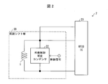
- FIG. 2 is a block diagram illustrating a main configuration of the non-contact communication circuit 2 including the antenna 1 according to the present embodiment.
- the non-contact communication circuit 2 includes a tuning shift unit 20 and an RFID IC (integrated circuit) 23.
- the non-contact communication circuit 2 is a non-contact communication circuit having both an RFID card function and an RFID reader / writer function.
- the tuning shift unit 20 functions to shift the resonance frequency, and includes the antenna 1 and the external control variable capacitor 22.
- the antenna 1 communicates with an external device by transmitting or receiving radio waves.
- the external control variable capacitor 22 receives a control signal from the outside, and changes the capacity of the external control variable capacitor 22, thereby transmitting and receiving radio waves via the antenna 1. Change the resonance frequency.
- the antenna 1 and the external control variable capacitor 22 form a parallel resonance circuit.
- the RFID IC 23 operates a built-in control circuit and a memory by the power generated by the tuning shift unit 20 and performs necessary information processing.
- the antenna 1 is applied to a contactless communication circuit having both the RFID card function and the RFID reader / writer function.
- the antenna 1 has an RFID card function (RFID tag function). You may apply to the portable terminal device etc. which were equipped with.
- the antenna according to the present embodiment is formed by forming a rib (rib-like structure) on the reference surface and providing an antenna pattern on the outer surface of the rib.
- FIG. 3A is a perspective view showing an antenna 1c according to the present embodiment.
- the antenna pattern 11 a is formed on the outer surface of the rib 13 on the plane T ⁇ b> 10 that is a reference surface of the housing (base) 15.
- the antenna pattern 11 a is connected to the power supply pad portion 14.
- the casing 15 include a casing of a mobile terminal, an RFID tag, a non-contact IC card, an RFID reader / writer, and the like.
- the housing 15 may be a resin housing.
- the multiple loop structure of the rib 13 will be specifically described.
- three large, medium and small frame-shaped ribs 13 are formed, and medium-sized ribs 13 are formed so as to surround the small ribs 13.
- a large rib 13 is formed so as to surround the medium-sized rib 13. That is, the rib 13 is formed in a spiral structure in which a predetermined interval is provided between adjacent loops having different sizes.
- the rib 13 may be formed by digging down, may be formed by adhering the formed rib 13 to the plane T10, or may be formed by providing irregularities on the resin casing itself.
- Antenna patterns 11 a are formed on the outer surfaces of the three ribs 13, and the antenna patterns 11 a formed on one rib 13 are connected in series to the antenna patterns 11 a formed on the adjacent ribs 13.
- the power feeding pad portion 14 is formed on the plane T10 located inside and outside the rib 13.
- the power supply pad portion 14 is connected to the substrate circuit via a power supply spring.
- the antenna 1c is operated by making the power supply pad portion 14 conductive.
- the antenna pattern 11a is the same as the method described in the first embodiment, and a description thereof is omitted here.
- the antenna pattern is preferably formed (plated) integrally with the housing by plating a housing such as a resin.
- a housing such as a resin.
- substrate) become unnecessary. Therefore, the cost for forming the antenna can be suppressed.
- FIG. 3B is a perspective view showing the rib 13 and the antenna pattern 11a according to the present embodiment.
- the rib 13 has three outer surfaces for forming the antenna pattern 11a. Of the three outer surfaces, two are the planes T11 and T13 constituting the side surface of the rib 13, and have a height L7. The remaining one plane is a plane parallel to the plane T10 and is a plane T12 that forms the upper surface of the rib 13.
- the plane T12 has a width L6.
- the antenna pattern 11a is continuously formed from at least a part of the plane T11 to at least a part of the plane T12. That is, the antenna pattern 11 a includes a polygonal line shape along the polygonal line shape of the rib 13.
- the width of the antenna pattern 11a is L6 + L7. Therefore, the line width of the antenna pattern 11a according to this embodiment and the antenna pattern 11b described later can be formed wider than the width L6 that is the width of the rib 13.
- the antenna pattern 11a may be formed so that the cross-sectional shape is a polygonal line shape over the entire plane T11 and the plane T10 adjacent to the plane T11.
- FIG. 3C is a perspective view showing the rib 13 and the antenna pattern 11b according to this modification.
- the antenna pattern 11b is formed over the entire three planes T11, T12, and T13 of the rib 13.
- the antenna pattern 11b may be formed so that a cross-sectional shape may become a polygonal line shape over the plane T10 adjacent to the plane T11 and the plane T13.
- FIGS. 4A to 4L are diagrams showing variations in the formation position of the antenna pattern 11c according to this modification.
- 4A to 4L show the rib 13 and the antenna pattern 11c in a cross section perpendicular to the plane T10 of the housing 15.
- FIG. The line width of the antenna pattern 11c shown in FIGS. 4A to 4L is all wider than the width L6 of the rib 13.
- 4B is formed over the entire plane T11 and the plane T10 adjacent to the plane T11.
- the antenna pattern 11c shown in FIG. 4C is formed over the entire plane T11, a part of the plane T12 that forms the upper surface of the rib 13, and the plane T10 adjacent to the plane T11.
- 4D is formed over the entire plane T11, the entire plane T12, and the plane T10 adjacent to the plane T11.
- the antenna pattern 11c shown in FIG. 4E includes the entire plane T11, the entire plane T12, a part of the plane T13 that forms the other side surface of the rib 13, and a plane T10 adjacent to the plane T11. It is formed over.
- the antenna pattern 11c is formed across the entire plane T11, the entire plane T12, the entire plane T13, and the plane T10 adjacent to the plane T11.
- the antenna pattern 11c shown in FIG. 4G is formed on the entire plane T11, the entire plane T12, the entire plane T13, the plane T10 adjacent to the plane T11, and the plane T10 adjacent to the plane T13. It is formed over.
- the antenna pattern 11c shown in (h) of FIG. 4 is formed over the entire plane T11 and a part of the plane T12.
- the antenna pattern 11c shown in (i) of FIG. 4 is formed over the entire plane T11 and the entire plane T12.
- the antenna pattern 11c shown in (j) of FIG. 4 is formed over the entire plane T11, the entire plane T12, and a part of the plane T13.
- the antenna pattern 11c shown in FIG. 4 (k) is formed over the entire plane T11, the entire plane T12, and the entire plane T13.
- the antenna pattern 11c shown in (l) of FIG. 4 is formed over a part of the plane T11, the entire plane T12, and a part of the plane T13.
- the surface which comprises a rib is not limited to a plane,
- a curved surface may be sufficient.
- the rib may be configured by combining a flat surface and a curved surface.
- the antenna 1c is an antenna in which the antenna pattern is formed in the loop structure on the casing 15, and the casing 15 has the ribs 13 along the loop structure. At least a part of the antenna pattern is formed on the outer surface of the structure of the rib 13, and the antenna pattern conforms to a polygonal line shape, a curved shape, or a combination of the ribs 13 in a cross section perpendicular to the housing 15. , A polygonal line shape, a curved line shape, or a combination thereof.
- the antenna patterns 11, 11 a, 11 b, and 11 c are formed on at least a part of the inner surface of the groove-shaped structure, or a rib shape And an antenna formed on at least a part of the outer surface of the structure.
- the antenna patterns 11, 11 a, 11 b, and 11 c have at least a part of the inner surface of the groove-shaped structure or the outer surface of the rib-shaped structure, and other than the above structure.
- the antenna formed also in the plane (T4, T10) is included.
- a part of the antenna pattern 31 is formed on the rib 33 formed on the casing 32 of the mobile terminal.
- FIG. 5 is a figure which shows the space which the housing
- the housing 32 has a space for storing the circuit configuration unit 34, the circuit configuration unit 34 b, and the battery unit 35.
- FIG. 5B is a diagram showing the antenna 1d formed on the plane T14 forming the reference plane of the housing 32.
- the antenna pattern 31 constituting the antenna 1d is formed on the outer surface of the plane T14 and the rib 33 on the plane T14.
- the antenna 1d is formed as a double loop structure (spiral structure). Note that the loop structure of the antenna 1d is not limited to double, and may be triple or more, for example, or may be single.
- FIG. 5C is a view showing a cross section taken along the line BB of FIG.
- a part of the region R2 where the antenna pattern 31 is formed on the plane T14 is located below the space in which the circuit configuration unit 34 is stored.
- the power supply pad portion 36 is formed in the region R ⁇ b> 2, and the antenna pattern 31 is connected to the power supply pad portion 36.
- the power supply pad portion 36 is connected to the circuit configuration portion 34 via a power supply spring 38.
- the antenna 1d is operated by making the power supply pad portion 36 and the circuit configuration portion 34 conductive.
- a display unit 37 is provided on the upper portion of the housing 32.
- the circuit configuration unit 34 is stored above the housing 32 (on the display unit 37 side), and the antenna pattern 31 is on the plane T14 in a region where there is no space to expand in the direction perpendicular to the plane T14. Is formed.
- FIG. 5D is a view showing a cross section taken along the line CC of FIG.
- FIG. 5D is a view showing a cross section taken along the line CC of FIG.
- a part of the space formed in the region R1 is used for forming the rib 33, and the rest of the space is used for storing the circuit component 34b.
- the rib 33 has two planes that form the side surfaces of the rib 33 that are perpendicular to the plane T14 and parallel to each other in the vertical cross section of the plane T14, and the upper surface of the rib 33 that is parallel to the plane T14. And a single flat surface.
- the rib 33 is formed with a width L8 in a cross section perpendicular to the plane T14.
- the antenna pattern 31 is formed on the outer surface of the rib 33 so that the cross-sectional shape includes a polygonal line shape so that the line width is wider than the width L ⁇ b> 8 of the rib 33. ing.
- the said space can be effectively utilized by forming the rib 33 in the space currently expand
- the antenna pattern 31 on the rib 33 or the plane T14 according to the space in the housing 32, the size and / or thickness of the mobile terminal can be reduced.
- the antenna pattern on the outer surface of the rib 33 formed in the space extending in the direction perpendicular to the plane T14 the line width of the antenna pattern is widened. Therefore, an antenna with good performance can be formed.
- the casing of the mobile terminal is designed to ensure the maximum battery capacity.
- the width of the storage space of the battery unit 35 is often set close to the housing 32. Therefore, the width of the battery portion 35 and the housing 32 on the plane T14 is extremely small, and the circuit components arranged in the space having the width are limited to small components. Therefore, the space tends to be a dead space.
- the antenna 1d according to the present embodiment by forming the ribs 33 in the dead space that develops in the direction perpendicular to the plane T14, an antenna pattern with as wide a line width as possible can be formed.
- the circuit configuration unit 34 includes a plurality of circuit boards on which circuit components are mounted. Therefore, in the upper or lower region of the circuit configuration unit 34, a space cannot be developed in the direction perpendicular to the plane T14.
- the antenna pattern 31 that requires a space in the direction perpendicular to the plane T14 is formed in the upper or lower region of the circuit configuration unit 34, there is a demerit that the size of the housing 32 must be increased.
- the antenna 1d when there is no space in the vertical direction with respect to the plane T14, the antenna pattern 31 is formed on the plane T14. Therefore, the increase in the size of the housing 32 can be suppressed.
- a thin film pattern (antenna patterns 11, 11a, 11b) of a conductor is formed in a loop structure on a base (casings 15 and 32, a substrate 12).
- the antenna device (antennas 1, 1a to d) has a groove-like structure (grooves 3, 3a, 3b) or a rib-like structure (ribs 13, 33) along the loop structure.
- at least a part of the thin film pattern of the conductor is formed on the inner surface of the groove-shaped structure or the outer surface of the rib-shaped structure, and the thin film pattern of the conductor is perpendicular to the base.
- the cross section includes a polyline shape, a curve shape, or a combination thereof along the shape of a polyline, a curve, or a combination of the groove-like or rib-like structures.
- the rib-shaped or groove-shaped structure includes a polygonal line shape or a curved line shape, for example, as in a mode in which the cross-sectional shape is rectangular. Therefore, the thin film is formed such that the shape (cross-sectional shape) of the cross section perpendicular to the base includes a polygonal line shape or a curved shape along the outer surface of such a three-dimensional rib-shaped structure or the inner surface of the groove-shaped structure.
- a pattern can be formed.
- the length (line width of the thin film pattern) from one end to the other end of the above-mentioned cross-sectional shape of the thin film pattern is changed to an antenna device in which the thin film pattern is formed only on one plane.
- the thin film pattern can be formed longer. That is, the thin film pattern can have a wide line width.
- a thin film pattern having a predetermined line width can be formed in a narrower region on the substrate surface than in the prior art.
- the inner surface of the groove-like structure may be composed of a combination of a plurality of planes, may be composed of one curved surface or a combination of a plurality of curved surfaces, or may be composed of one or a plurality of planes and one or more It may be composed of a combination of a plurality of curved surfaces.
- the antenna device is the antenna apparatus according to aspect 1, wherein the thin film pattern of the conductor is formed on at least a part of the inner surface of the groove-shaped structure, or the outer surface of the rib-shaped structure. It may be formed at least partially.
- the thin film pattern is formed in at least one part of the inner surface of the said groove-shaped structure, or is formed in a part of outer surface of the said rib-shaped structure. Therefore, a conductor thin film pattern having a wide line width can be formed by using a part of the inner or outer surface of the three-dimensional structure.
- the thin film pattern is formed on the entire inner surface or outer surface of the structure, and the aspect formed on a part of the inner surface or outer surface of the structure and the surface other than the structure on the base. Is included.
- the antenna device may be formed over at least a part of the inner surface or outer surface of the structure and a surface of the base other than the structure in the aspect 2.
- the thin film pattern is formed ranging from the inner surface or a part of outer surface of the said structure to surfaces other than the said structure in the said base. Therefore, the line width of the thin film pattern of the conductor can be formed wider.
- the loop structure may be a spiral structure including a plurality of loop structures.
- a thin film pattern having a predetermined line width can be formed in a narrower region on the substrate surface than in the prior art. Therefore, according to the aspect 4 in which the aspect 1 is applied to the spiral structure in which the thin film pattern is rotated a plurality of times, the arrangement area of the thin film pattern for each turn can be narrowed. Therefore, the area of a region necessary for forming a spiral-shaped thin film pattern having a plurality of loop structures can be greatly suppressed.
- the mobile terminal device may include the antenna device according to aspects 1 to 4.
- the said portable terminal device can be equipped with an antenna with a long communication distance or a high communication sensitivity in the limited area
- the mobile terminal device can be downsized.
- the non-contact communication device may include the antenna device according to aspects 1 to 4.
- a non-contact communication device such as an RFID tag, a non-contact IC card, or an RFID reader / writer can be provided with an antenna having a long communication distance or good communication sensitivity in a limited area.
- the contactless communication device can be reduced in size.
- the present invention can be used for an antenna device, a portable terminal incorporating the antenna device, an RFID tag, a non-contact IC card, an RFID reader / writer, and the like.
- 1, 1a to d antenna antenna (antenna device), 2, non-contact communication circuit (non-contact communication device), 3, 3a, 3b groove (groove-like structure), 11, 11a, 11b antenna pattern (conductor thin film pattern), 12, 32 substrate (base), 13, 33 rib (rib-like structure), 15 housing (base)
Landscapes
- Engineering & Computer Science (AREA)
- Microelectronics & Electronic Packaging (AREA)
- Computer Networks & Wireless Communication (AREA)
- Computer Hardware Design (AREA)
- Physics & Mathematics (AREA)
- General Physics & Mathematics (AREA)
- Theoretical Computer Science (AREA)
- Details Of Aerials (AREA)
Abstract
限られた領域において広い線幅の導体の薄膜パターンを有するように、導体の薄膜パターン(アンテナパターン11、11a、11b)のループ構造に沿って、溝状(溝部3、3a、3b)、または、リブ状(リブ13、33)の構造を有し、導体の薄膜パターンは、上記構造の内面、または、外面に形成されており、上記導体の薄膜パターンは、上記土台に垂直な断面において、折れ線形状または曲線形状に沿った折れ線形状または曲線形状を含んでいる。
Description
本発明は、アンテナ装置、当該アンテナ装置を内蔵する携帯端末、RFIDタグ、非接触ICカード、RFIDリーダライタ等に関する。
現在までに、携帯電話、または、RFID(Radio Frequency Identification)システムなどによる無線通信において、内蔵型のアンテナ装置の技術が開発されている。内蔵型のアンテナ装置として、アンテナとして機能するループ形状のアンテナパターン(導体の薄膜パターン)を備えた装置が普及している。上述のようなアンテナに関する技術として、例えば、特許文献1には、筐体の小型化を図りつつ通信効率の向上を図り得ることを目的とした携帯端末装置が開示されている。具体的には、筐体内にアンテナと電池とが配設されてなる携帯端末装置において、アンテナを可撓性を有するケーブルにより構成し、かつ電池を囲繞するよう配置している。
ところで、アンテナパターンは、その線幅が広くなると、アンテナパターンの電気抵抗の値は小さくなる。したがって、アンテナパターンの線幅が広いと、アンテナパターンに電流を流すことによって生じる磁力は強くなる、あるいは、アンテナパターンを通る磁束の変化によって発生する誘導電流が強くなるので、当該アンテナの通信距離が長くなる。
一方、アンテナパターンのループ形状に囲まれた領域(開口領域)の面積と、当該アンテナパターンに電流を流すことによって生じる磁束の量は比例する。あるいは、上記面積が広いほど、アンテナパターンの開口領域を通る磁束の量が増えるので、その磁束の変化によって発生する誘導電流が強くなる。したがって、アンテナの開口領域が広いと、当該アンテナの通信距離が長くなる。
しかしながら、上述のような従来技術は、筐体の小型化を図ることに特化しており、限られた領域においてアンテナパターンの線幅を広く形成するという観点から開発された技術ではない。そのため、限られた領域においてアンテナパターンの線幅を広く形成することは困難であった。
本発明の目的は、限られた領域において広い線幅のアンテナパターンを有するアンテナ装置を実現することにある。
上記の課題を解決するために、本発明の一態様に係るアンテナ装置は、土台に導体の薄膜パターンがループ構造に形成されているアンテナ装置であって、上記土台は、上記ループ構造に沿って、溝状、または、リブ状の構造を有し、上記導体の薄膜パターンの少なくとも一部は、上記溝状の構造の内面、または、上記リブ状の構造の外面に形成されており、上記導体の薄膜パターンは、上記土台に垂直な断面において、上記溝状、または、上記リブ状の構造の折れ線形状、曲線形状、またはその組み合わせの形状に沿った、折れ線形状、曲線形状、またはその組み合わせの形状を含んでいる。
本発明の一態様によれば、限られた領域において広い線幅のアンテナパターンを形成することが可能となり、導体の薄膜パターンが基準面にのみ形成されているアンテナ装置に比べ、通信距離を伸ばす、または通信感度を高めることができるという効果を奏する。
本明細書においては、アンテナを構成する導体の薄膜パターンを「アンテナパターン」とする。また、アンテナパターンの形成に用いる土台(基板)の上面に凹凸をつけることによって溝状またはリブ状の構造を形成するが、当該構造に隣接した上記上面を基準面とする。さらに、アンテナパターンの上記基準面に垂直な断面形状の一端から他端までの長さを「アンテナパターンの線幅」または「アンテナパターンの幅」とする。
(参考形態)
図7は、参考技術に係るアンテナ101および101aを例示する図である。
図7は、参考技術に係るアンテナ101および101aを例示する図である。
図7の(a)および(c)は、参考形態に係るアンテナ101、アンテナ101aの平面図をそれぞれ示している。
図7の(a)および(c)に示すように、基板112上にアンテナパターン111、または、アンテナパターン111aを形成することによって、アンテナ101およびアンテナ101aは形成されている。
基板112は矩形の形状であり、中央部には矩形の空間である開口領域が設けられており、上記開口領域には基板112は存在していない。図7の(a)に示すアンテナ101においては開口領域S11が設けられており、図7の(c)に示すアンテナ101aにおいては開口領域S12が設けられている。基板112上にはアンテナパターン111または111aが、矩形の螺旋形状に形成されている。
図7の(e)は、アンテナ101に電流が流された場合に生じる磁束を示す模式図である。図7の(e)に示すように、アンテナが形成されている基準面において、磁束の向きM1、M2、M3は、当該面に対して垂直の方向となる。例えば、当該アンテナ101がRFIDタグに提供された場合、上記基準面は、通信時にRFIDリーダライタ機器に対してかざす面とみなすことができる。
ここで、アンテナパターンの線幅とアンテナ特性との関係、および、アンテナの開口領域の面積とアンテナ特性との関係について図7を用いて説明する。なお、「アンテナパターンの線幅(幅)」とは「アンテナパターンの基準面(土台)に垂直な断面形状の一端から他端までの長さ」とする。
図7の(b)は図7の(a)のD-D線における断面を示す図であり、図7の(d)は図7の(c)のE-E線における断面を示す図である。
初めに、アンテナパターンの線幅とアンテナ特性との関係を説明する。図7の(b)に示すように、アンテナ101が形成されている基板112の幅は幅W1であり、螺旋形状を形成する各周のアンテナパターン111の線幅は幅L1である。一方で、図7の(d)に示すようにアンテナ101aが形成されている基板112の幅はW3であり、螺旋形状を形成する各周のアンテナパターン111aの線幅は幅L12である。幅L12は、幅L1よりも広く設定されている。よって、上述したアンテナパターンの線幅の観点で、通信距離を長くしようとすると、アンテナ101よりもアンテナ101aの方が有利である。
次に、アンテナの開口領域の面積とアンテナ特性との関係を図7を用いて説明する。図7の(b)および(d)に示すように、線幅の広いアンテナパターンを形成するためには、基板112の幅を広くする必要がある。したがって、広い線幅のアンテナパターンによって形成されているアンテナ101aが基板112上において形成されている領域の幅W3は、アンテナ101が基板112上において形成されている領域の幅W1よりも広くなる。よって、図7の(a)および(c)に示すように、アンテナ101aの開口領域S12の面積は、アンテナ101の開口領域S11の面積よりも狭くなる。そのため、上述したアンテナの開口領域の面積の観点で、通信距離を長くしようとすると、アンテナ101aよりもアンテナ101の方が有利である。
すなわち、上記2つの観点を考慮することが好ましい。具体的には、開口領域を稼ぐように限られた領域に、できるだけ線幅の広いアンテナパターンを形成することが好ましい。しかし、本参考形態においてはアンテナパターンの形成位置とアンテナの開口領域の位置とが、限られた面積の同一平面に位置している。そのため、限られた領域に線幅の広いアンテナパターンを形成することが困難である。
〔実施形態1〕
以下、本発明の一実施形態に係るアンテナ(アンテナ装置)1について、図1~図2に基づいて説明すれば、以下のとおりである。但し、本実施形態およびその他の実施形態に記載されている構成部品の寸法、材質、形状、その相対配置などは特に特定的な記載がない限り、この発明の範囲をそれのみに限定する趣旨ではなく、単なる説明例に過ぎない。
以下、本発明の一実施形態に係るアンテナ(アンテナ装置)1について、図1~図2に基づいて説明すれば、以下のとおりである。但し、本実施形態およびその他の実施形態に記載されている構成部品の寸法、材質、形状、その相対配置などは特に特定的な記載がない限り、この発明の範囲をそれのみに限定する趣旨ではなく、単なる説明例に過ぎない。
図1は、本実施形態に係るアンテナ1の一例を示す図である。図1の(a)は、本実施形態に係るアンテナ1の平面図を示している。図1の(a)に示すように、基板(土台)12上にアンテナパターン11を形成することによって、アンテナ1は形成されている。なお、以下では、基板12は矩形の形状であり、中央部には矩形の空間である開口領域S1が設けられ、開口領域S1には基板12は存在していない構成を例に説明する。一方で、本発明は上記の構成に限らず、例えば、基板の中央部において基板が存在しているが、当該中央部においてはアンテナパターンが形成されていない構成であってもよい。
基板12の上記基準面には、アンテナパターン11が、矩形のループを複数巻きにし、隣り合うループ間に所定間隔を設けた螺旋形状に形成されている。
ここで、基板12は、例えば、フレキシブル基板(FPC(Flexible printed circuits))などである。なお、本実施形態において、説明の便宜上、アンテナパターン11を基板12上に形成する例を挙げているが、アンテナパターン11はアンテナ1を内蔵する装置の樹脂筐体などの表面に形成されてもよい。アンテナパターン11は、銅およびニッケルのメッキ、または、銅、ニッケルおよび金のメッキによって形成されてもよい。また、アンテナパターン11は、導電性ペースト材を用いたプリント(印刷)によって形成されてもよいし、板金インサート成型によって形成されてもよい。
次に、本実施例に係るアンテナパターン11の断面形状について説明する。なお、本明細書に記載の溝、リブの断面形状、すなわち、アンテナパターンの断面形状については、辺の数、長さ、隣り合う2辺のなす角度は任意である。さらに、すべての辺が直線の場合に限らず、一部または全部の辺が曲線でもよい。図1の(b)は、図1の(a)におけるA-Aの断面を示す図である。図1の(b)に示す断面は、アンテナパターン11において、アンテナパターン11が螺旋形状を形成する基準面(平面T4)に垂直な断面形状を示している。また、基準面(平面T4)は、下記の溝部3または後述のリブ13のような溝状またはリブ状の構造が形成される面でもある。図1の(b)に示すように、基板12には溝部(溝状の構造)3が形成されており、溝部3の断面は矩形の一辺が開放された略「コ」の字状である。すなわち、溝部3は、基板12の基準面に垂直な平面T2および平面T3、基準面に平行な平面T1から構成されている。なお、本実施形態においては、溝部3の断面形状を略「コ」の字状として例示しているが、上記形状は、当該断面形状が折れ線形状を含んだ態様の一例である。したがって、溝部3の断面形状は例えば、節が複数の折れ線形状などでもよい。
アンテナパターン11は、溝部3の平面T1、T2およびT3のうち、少なくとも隣接した2面上に形成されている。また、アンテナパターン11は、上記溝部3を形成する平面T1、T2およびT3に加え、溝部3に隣接する基板12上の平面T4に連続して形成されていてもよい。アンテナパターン11は、線幅が均一に形成されていてもよい。なお、図1の(b)に示すように、本実施形態に例示するアンテナパターン11の線幅は均一でなくてもよい。上記の構成によると、基板12の構造に応じてアンテナパターン11を形成することができる。すなわち、アンテナパターン11は、アンテナ1が形成されている基準面に平行ではない面に少なくとも形成されており、かつ、アンテナパターン11は、当該線幅の断面において隣接した2つ以上の平面に亘って形成されている。なお、基準面に平行ではない平面とは、アンテナ1に電流を流すことにより発生する磁束の向きM1~M3(図7の(e))と直交する平面に平行でない平面ともいえる。
次に、本実施形態と上述の参考形態とのアンテナパターン形成領域について比較する。例えば、図1の(b)および図7の(b)に示すように、本実施形態に係るアンテナパターン11は、基準面(平面T4)を平面視したとき、幅L1で形成されており、参考形態に係るアンテナパターン111においても、基板112を平面視したとき、同じ幅L1に形成されている。
一方で、本実施形態に係るアンテナパターン11は、基準面に平行な平面T1に加え、平面T4に垂直な平面T2および/またはT3においても形成されている。そのため、アンテナパターン11の線幅は、平面T2および/または平面T3上に形成されたアンテナパターン11の幅が幅L1に加わる。例えば、図1の(b)に示すように、アンテナパターン11が平面T2上およびT3上において幅L2で形成された場合、アンテナパターン11の線幅は、幅L1+幅L2×2となる。
したがって、アンテナパターン11の1ループの設置に必要な領域の幅は幅L1となるが、実際のアンテナパターン11の幅は幅L1+幅L2×2となる。よって、参考形態におけるアンテナ101の形成領域の幅W1と本実施形態におけるアンテナ1の形成領域の幅W1とが同じであったとしても、本実施形態のアンテナパターン11の線幅を、参考形態のアンテナパターン111の線幅より広くすることが可能となる。
(アンテナ特性)
ここで、アンテナパターンの線幅を変化させた場合の通信特性について説明する。図6は、共振周波数に対する通信距離の変化と、アンテナパターンの線幅との関係を示す図である。
ここで、アンテナパターンの線幅を変化させた場合の通信特性について説明する。図6は、共振周波数に対する通信距離の変化と、アンテナパターンの線幅との関係を示す図である。
本実施例では、同一外形サイズのアンテナ(同一ターン数)において、線幅が0.3mm、0.4mmおよび0.5mmのアンテナパターン形成し、それぞれのアンテナにおける共振周波数(X軸)-通信距離(Y軸)特性をプロットしたデータである。
図6に示すように、線幅を太くした場合にアンテナの通信距離が顕著に伸びていることがわかる。
(変形例1)
次に、図1の(c)を用いて、本変形例に係るアンテナ1aについて説明する。本変形例に係る溝部3aは、基準面に対する垂直な断面の形状が三角形の一辺が開放された略「V」字状である。図1の(c)は、本変形例に係るアンテナ1aにおける断面を示す図であり、アンテナパターン11において、上記基準面(平面T4)に垂直な断面形状を示している。図1の(c)に示すように、基板12の基準面には溝部3aが形成されており、溝部3aは、基準面に垂直な平面からなる平面T6および基準面に対して任意の斜角を有する平面T5から構成されている。なお、上記の基準面に対する平面T6および平面T5の斜角は、当該断面形状が折れ線形状を含んだ態様の一例である。したがって、平面T6および平面T5の任意の角度であってもよい。
次に、図1の(c)を用いて、本変形例に係るアンテナ1aについて説明する。本変形例に係る溝部3aは、基準面に対する垂直な断面の形状が三角形の一辺が開放された略「V」字状である。図1の(c)は、本変形例に係るアンテナ1aにおける断面を示す図であり、アンテナパターン11において、上記基準面(平面T4)に垂直な断面形状を示している。図1の(c)に示すように、基板12の基準面には溝部3aが形成されており、溝部3aは、基準面に垂直な平面からなる平面T6および基準面に対して任意の斜角を有する平面T5から構成されている。なお、上記の基準面に対する平面T6および平面T5の斜角は、当該断面形状が折れ線形状を含んだ態様の一例である。したがって、平面T6および平面T5の任意の角度であってもよい。
また、アンテナパターン11は、溝部3aを構成する平面T5およびT6に加え、溝部3aに隣接する基板12上の平面T4に連続して形成されていてもよい。すなわち、アンテナパターン11は、少なくとも、基準面に平行ではない面に形成されており、かつ、アンテナパターン11は、当該線幅の断面において隣接した2つ以上の平面に亘って形成されている。
次に、本変形例と上述の参考形態とのアンテナパターン形成領域について比較する。図1の(c)に示すように、本実施形態に係るアンテナパターン11は、基準面(平面T4)を平面視したとき、幅L5で形成されている。幅L5は、図7の(b)に示す参考形態に係るアンテナパターン111の幅L1よりも狭い。
さらに、アンテナパターン11は、溝部3aを構成する平面T5、および、平面T6に形成されている。平面T5に形成されているアンテナパターン11の幅は幅L3であり、平面T6に形成されているアンテナパターン11の幅は幅L4である。ここで、幅L3と幅L4との和は、参考形態のアンテナパターン111の幅L1より広い。すなわち、アンテナパターン11が形成される幅L5は、幅L1より狭いにもかかわらず、本変形例に係るアンテナパターン11の線幅の方が参考形態に係るアンテナパターンの線幅よりも広い。したがって、基板12において、アンテナ1aを形成するのに要する領域の幅W2を、アンテナ101の幅W1より狭くすることができる。この効果の程度は、ループの数が多いほど高くなる。
上記の構成によれば、溝部3aの内面を利用して、基板12が形成する平面T4とは平行ではない面に、アンテナパターン11を形成するため、アンテナパターンの線幅を広くしつつ、基板12上のアンテナの形成領域を狭くすることができる。よって、アンテナ開口領域を広くすることが可能となり、限られた領域に形成されたアンテナにおいても通信性能を高めることが可能となる。
(変形例2)
次に、図1の(d)を用いて、本変形例に係るアンテナ1bについて説明する。本変形例に係る溝部3bは、基準面に対する垂直な断面形状が円弧形状である。図1の(d)は、アンテナ1bにおける、断面を示す図であり、アンテナパターン11において、基準面(平面T4)に垂直な断面形状を示している。
次に、図1の(d)を用いて、本変形例に係るアンテナ1bについて説明する。本変形例に係る溝部3bは、基準面に対する垂直な断面形状が円弧形状である。図1の(d)は、アンテナ1bにおける、断面を示す図であり、アンテナパターン11において、基準面(平面T4)に垂直な断面形状を示している。
図1の(d)に示すように、基板12の基準面には溝部3bが形成されており、溝部3bの平面T4に対して垂直な断面における形状は円弧形状である。すなわち、溝部3bは、円弧形状の曲面T7から構成されている。なお、円弧形状は、当該断面形状が曲線を含んだ態様の一例である。したがって、溝部3bの断面形状は円弧形状に限定されず、例えば、楕円の円周の一部、または放物線の一部を示す形状などでもよい。
アンテナパターン11は、溝部3bの曲面T7の少なくとも一部に形成されていればよく、曲面T7上の全体に亘って形成されていてもよい。また、アンテナパターン11は、上記溝部3bを形成する曲面T7の少なくとも一部に加え、溝部3bに隣接する平面T4上に連続して形成されていてもよい。
次に、本変形例と上述の参考形態とのアンテナパターン形成領域について比較する。本変形例に係るアンテナパターン11は、溝部3bに形成されている。詳細には、アンテナパターン11は、溝部3bを形成する曲面T7に形成されている。溝部3bの幅は幅L1であり、参考形態に係るアンテナパターン111の幅L1と同じである。上述のように曲面T7は曲面であるため、アンテナパターン11の幅を、幅L1よりも広くすることができる。よって、参考形態のアンテナ111と本変形例のアンテナ1bとを形成するのに要する領域の幅W1が互いに同じであったとしても、アンテナパターン11の線幅を、アンテナパターン111の線幅よりも広くすることが可能となる。
すなわち、本実施形態に係るアンテナ1,1aまたは1bは、基板12にアンテナパターン11がループ構造に形成され、基板12は、上記ループ構造に沿って、溝部3、3aまたは3bの構造を有し、アンテナパターン11の少なくとも一部は、溝部3、3aまたは3bの内面に形成されており、アンテナパターン11は、基板12に垂直な断面において、溝部3、3aまたは3bの折れ線形状または曲線形状に沿った折れ線形状または曲線形状を含んでいる。なお、上述の本実施形態に示す溝部の断面形状は、折れ線形状または曲線形状を含んでいる形状を例示したが、溝部の断面形状が折れ線形状および曲線形状の組合せから構成されていてもよく、その場合、アンテナパターンの断面形状は折れ線形状および曲線形状の組み合わせの形状を含む。
(非接触通信装置)
次に、本実施形態に係るアンテナ1を備えている非接触通信装置2について図2を用いて説明する。図2は、本実施形態に係るアンテナ1を備えている非接触通信回路2の要部構成を示すブロック図である。非接触通信回路2は、同調シフト部20およびRFID IC(integrated circuit)23を備えている。非接触通信回路2は、RFIDカード機能とRFIDリーダライタ機能の両機能を備えた非接触通信回路である。同調シフト部20は、共振周波数をシフトさせる働きをし、アンテナ1と外部制御可変コンデンサ22とを備えている。アンテナ1は、電波を送信、または受信して外部機器と通信を行なうものである。RFIDカード機能時及びRFIDリーダライタ機能時において、外部制御可変コンデンサ22は、外部から制御信号を受信して、外部制御可変コンデンサ22の容量を変化させることにより、アンテナ1を介して送受信する電波の共振周波数を変化させる。アンテナ1と外部制御可変コンデンサ22とは、並列共振回路を形成している。RFID IC23は、同調シフト部20で発生した電力により、内蔵の制御回路およびメモリを動作させ、必要な情報処理を行う。
次に、本実施形態に係るアンテナ1を備えている非接触通信装置2について図2を用いて説明する。図2は、本実施形態に係るアンテナ1を備えている非接触通信回路2の要部構成を示すブロック図である。非接触通信回路2は、同調シフト部20およびRFID IC(integrated circuit)23を備えている。非接触通信回路2は、RFIDカード機能とRFIDリーダライタ機能の両機能を備えた非接触通信回路である。同調シフト部20は、共振周波数をシフトさせる働きをし、アンテナ1と外部制御可変コンデンサ22とを備えている。アンテナ1は、電波を送信、または受信して外部機器と通信を行なうものである。RFIDカード機能時及びRFIDリーダライタ機能時において、外部制御可変コンデンサ22は、外部から制御信号を受信して、外部制御可変コンデンサ22の容量を変化させることにより、アンテナ1を介して送受信する電波の共振周波数を変化させる。アンテナ1と外部制御可変コンデンサ22とは、並列共振回路を形成している。RFID IC23は、同調シフト部20で発生した電力により、内蔵の制御回路およびメモリを動作させ、必要な情報処理を行う。
なお、本実施形態においては、アンテナ1をRFIDカード機能とRFIDリーダライタ機能の両機能を備えた非接触通信回路に適用する例を示したが、アンテナ1をRFIDカード機能(RFIDタグの機能)を備えた携帯端末装置などに適用してもよい。
〔実施形態2〕
本発明の他の実施形態について、図3に基づいて説明すれば、以下のとおりである。なお、説明の便宜上、前記実施形態にて説明した部材と同じ機能を有する部材については、同じ符号を付記し、その説明を省略する。
本発明の他の実施形態について、図3に基づいて説明すれば、以下のとおりである。なお、説明の便宜上、前記実施形態にて説明した部材と同じ機能を有する部材については、同じ符号を付記し、その説明を省略する。
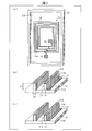
本実施形態に係るアンテナは、基準面にリブ(リブ状の構造)を形成し、当該リブの外面にアンテナパターンを設けることによって形成されている。図3の(a)は、本実施形態に係るアンテナ1cを示す斜視図である。図3の(a)に示すように、アンテナパターン11aは、筐体(土台)15の基準面である平面T10上のリブ13の外面に形成されている。また、アンテナパターン11aは給電パッド部14に連結している。筐体15は、例えば、携帯端末の筐体、RFIDタグ、非接触ICカード、RFIDリーダライタ等の筐体が挙げられる。筐体15は樹脂筐体であってもよい。
リブ13の多重ループ構造について具体的に説明する。平面T10には、大中小の3つの大きさの枠状のリブ13が形成されており、小さいリブ13を取り囲むように、中程度の大きさのリブ13が形成されている。また、中程度の大きさのリブ13を取り囲むように、大きいリブ13が形成されている。すなわち、リブ13は、サイズの異なる隣り合うループ間に所定間隔を設けた螺旋構造に形成されている。
上記リブ13は、掘り下げて形成されてもよいし、形成されたリブ13を平面T10に接着することによって形成されてもよいし、樹脂筺体自体に凹凸をつけることによって形成されてもよい。3つのリブ13の外面にはアンテナパターン11aが形成されており、あるリブ13に形成されているアンテナパターン11aは、隣接するリブ13に形成されているアンテナパターン11aに直列に連結している。
また、給電パッド部14は、リブ13よりも内側および外側に位置する平面T10上に形成されている。給電パッド部14は、給電用バネを介して基板回路に接続している。給電パッド部14を導通させることによって、アンテナ1cを動作させる。
アンテナパターン11aの形成方法は、実施形態1にて記載した方法と同様のためここでの説明を省略する。なお、本実施形態においては、アンテナパターンを樹脂などの筺体にメッキすることにより、筐体と一体に形成(メッキ)することが好ましい。従来の基準面にのみアンテナパターンが形成されているアンテナの場合、アンテナパターンを形成した硬質基板、FPC等を、筺体やホルダ部材に粘着テープ等を用いて貼り付け固定する必要があった。そのため、複数の部材が必要であった。上記の構成によれば、アンテナ形成用の基板やFPC(フレキシブル基板)が不要となる。したがって、アンテナ形成にかかるコストを抑えることができる。
次にリブ13における、アンテナパターン11aの形成位置について説明する。図3の(b)は、本実施形態に係るリブ13およびアンテナパターン11aを示す斜視図である。図3の(b)に示すように、リブ13は、アンテナパターン11aを形成するための3つの外面を有する。当該3つの外面のうち、2つはリブ13の側面を構成する平面T11およびT13であり、高さL7を有する。残りの1つの平面は、平面T10に平行な平面であり、リブ13の上面を形成する平面T12である。平面T12は幅L6を有する。
アンテナパターン11aは、一例として、平面T11の少なくとも一部から、平面T12の少なくとも一部に亘って連続的に形成されている。すなわち、アンテナパターン11aは、リブ13の折れ線形状に沿った折れ線形状を含んでいる。ここで、アンテナパターン11aの幅は、L6+L7となる。したがって、本実施形態に係るアンテナパターン11a、および、後述するアンテナパターン11bの線幅は、リブ13の幅である幅L6よりも広く形成することができる。なお、アンテナパターン11aは平面T11の全体および平面T11に隣接する平面T10に亘って、断面形状が折れ線形状となるように形成されていてもよい。
(変形例3)
次に、リブ13における、アンテナパターン11aの形成位置の変形例について説明する。図3の(c)は、本変形例に係るリブ13およびアンテナパターン11bを示す斜視図である。図3の(c)に示すように、アンテナパターン11bは、リブ13の上記3つの平面T11,T12およびT13の全体に亘って形成されている。なお、アンテナパターン11bは平面T11および平面T13に隣接する平面T10に亘って、断面形状が折れ線形状となるように形成されていてもよい。
次に、リブ13における、アンテナパターン11aの形成位置の変形例について説明する。図3の(c)は、本変形例に係るリブ13およびアンテナパターン11bを示す斜視図である。図3の(c)に示すように、アンテナパターン11bは、リブ13の上記3つの平面T11,T12およびT13の全体に亘って形成されている。なお、アンテナパターン11bは平面T11および平面T13に隣接する平面T10に亘って、断面形状が折れ線形状となるように形成されていてもよい。
(変形例4)
次に、リブ13における、アンテナパターン11aの形成位置のバリエーションについて説明する。図4の(a)から(l)は、本変形例に係るアンテナパターン11cの形成位置のバリエーションを示す図である。図4の(a)から(l)は、筐体15の平面T10に垂直な断面における、リブ13およびアンテナパターン11cを示している。なお、図4の(a)から(l)に示されるアンテナパターン11cの線幅は、リブ13の幅L6よりもすべて広く形成されている。
次に、リブ13における、アンテナパターン11aの形成位置のバリエーションについて説明する。図4の(a)から(l)は、本変形例に係るアンテナパターン11cの形成位置のバリエーションを示す図である。図4の(a)から(l)は、筐体15の平面T10に垂直な断面における、リブ13およびアンテナパターン11cを示している。なお、図4の(a)から(l)に示されるアンテナパターン11cの線幅は、リブ13の幅L6よりもすべて広く形成されている。
図4の(a)に示されるアンテナパターン11cは、リブ13の一方の側面を形成する平面T11の一部、および、平面T11に隣接する平面T10に亘って形成されている。
図4の(b)に示されるアンテナパターン11cは、上記平面T11の全体、および、平面T11に隣接する平面T10に亘って形成されている。
図4の(c)に示されるアンテナパターン11cは、上記平面T11の全体、リブ13の上面を形成する平面T12の一部、および、平面T11に隣接する平面T10に亘って形成されている。
図4の(d)に示されるアンテナパターン11cは、上記平面T11の全体、上記平面T12の全体、および、平面T11に隣接する平面T10に亘って形成されている。
図4の(e)に示されるアンテナパターン11cは、上記平面T11の全体、上記平面T12の全体、リブ13の他方の側面を形成する平面T13の一部、および、平面T11に隣接する平面T10に亘って形成されている。
図4の(f)に示されるアンテナパターン11cは、上記平面T11の全体、上記平面T12の全体、上記平面T13の全体、および、平面T11に隣接する平面T10に亘って形成されている。
図4の(g)に示されるアンテナパターン11cは、上記平面T11の全体、上記平面T12の全体、上記平面T13の全体、平面T11に隣接する平面T10、および、平面T13に隣接する平面T10に亘って形成されている。
図4の(h)に示されるアンテナパターン11cは、上記平面T11の全体、および、上記平面T12の一部に亘って形成されている。
図4の(i)に示されるアンテナパターン11cは、上記平面T11の全体、および、上記平面T12の全体に亘って形成されている。
図4の(j)に示されるアンテナパターン11cは、上記平面T11の全体、上記平面T12の全体、上記平面T13の一部に亘って形成されている。
図4の(k)に示されるアンテナパターン11cは、上記平面T11の全体、上記平面T12の全体、および、上記平面T13の全体に亘って形成されている。
図4の(l)に示されるアンテナパターン11cは、上記平面T11の一部、上記平面T12の全体、および、上記平面T13の一部に亘って形成されている。
なお、本変形例においては、平面T11、T12およびT13によって構成されているリブ13について例示したが、リブを構成する面は、平面に限定されず、例えば、曲面であってもよい。また、リブは平面と曲面とを組み合せて構成されていてもよい。
また、本変形例は、リブ13の外面に形成されるアンテナパターン11cのバリエーションについて説明したが、3つの面から成る溝部の内面にアンテナパターンを形成する場合においても、リブ13の外面を溝部の内面と解釈することによって上記バリエーションを同様に適用できる。
このように、本実施形態に係るアンテナ1cは、筐体15にアンテナパターンがループ構造に形成されているアンテナであって、筐体15は、上記ループ構造に沿って、リブ13を有し、アンテナパターンの少なくとも一部は、リブ13の構造の外面に形成されており、アンテナパターンは、筐体15に垂直な断面において、リブ13の折れ線形状、曲線形状、またはその組み合わせの形状に沿った、折れ線形状、曲線形状、またはその組み合わせの形状を含んでいる。
また、実施形態1および2に係るアンテナ1,1a,1b,1cは、アンテナパターン11,11a,11b,11cが上記溝状の構造の内面の少なくとも一部に形成されている、あるいは、リブ状の構造の外面の少なくとも一部に形成されているアンテナを含んでいる。
また、上述したアンテナ1,1a,1b,1cは、アンテナパターン11,11a,11b,11cが、溝状の構造の内面、または、リブ状の構造の外面の少なくとも一部と、上記構造以外の平面(T4,T10)にも形成されているアンテナを含んでいる。
〔実施形態3〕
本発明の他の実施形態について、図5に基づいて説明すれば、以下のとおりである。なお、説明の便宜上、前記実施形態にて説明した部材と同じ機能を有する部材については、同じ符号を付記し、その説明を省略する。
本発明の他の実施形態について、図5に基づいて説明すれば、以下のとおりである。なお、説明の便宜上、前記実施形態にて説明した部材と同じ機能を有する部材については、同じ符号を付記し、その説明を省略する。
本実施形態においては、携帯端末の筐体32に形成されたリブ33上にアンテナパターン31の一部が形成されている。
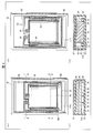
初めに、筐体32が有するスペースについて説明する。図5の(a)は、携帯端末の筐体32が有するスペースを示す図である。図5の(a)に示すように、筐体32は、回路構成部34、回路構成部34b、および、電池部35を格納するスペースを有している。
次に、筐体32に形成されているアンテナ1dについて説明する。図5の(b)は、筐体32の基準面を形成している平面T14に形成されているアンテナ1dを示す図である。図5の(b)に示すように、アンテナ1dを構成するアンテナパターン31は、平面T14、および、平面T14上のリブ33の外面に形成されている。アンテナ1dは2重のループ構造(螺旋構造)として形成されている。なお、アンテナ1dのループ構造は2重に限定されず、例えば、3重以上であってもよいし、1重であってもよい。
次に、アンテナパターン31が平面T14に形成されている領域R2について説明する。図5の(c)は、図5の(a)のB-Bにおける断面を示す図である。図5の(b)および(c)に示すように、アンテナパターン31が平面T14に形成されている領域R2の一部は、回路構成部34が格納されるスペースの下方に位置している。また、図5の(c)に示すように、領域R2には、給電パッド部36が形成されており、アンテナパターン31は、給電パッド部36に連結している。給電パッド部36は、給電用バネ38を介して回路構成部34に接続している。給電パッド部36と回路構成部34とを導通させることによって、アンテナ1dを動作させる。なお、筐体32の上部には、表示部37が設けられている。
このように、筐体32の上方(表示部37側)に回路構成部34を格納しており、平面T14に対して垂直方向に展開するスペースがない領域においては、アンテナパターン31は平面T14上に形成されている。
次に、リブ33が形成されている領域R1について説明する。図5の(d)は、図5の(a)のC-Cにおける断面を示す図である。図5の(d)に示すように、電池部35と筐体32との間には、平面T14に対して垂直方向に展開しているスペースがある。領域R1に形成されたそのスペースの一部はリブ33の形成に利用され、そのスペースの残りは、回路構成部34bの格納に利用されている。リブ33は平面T14の垂直な断面において、平面T14に垂直でありお互いに平行であるリブ33の側面を形成している2つの平面と、平面T14に平行でありリブ33の上面を形成している1つの平面とから形成されている。リブ33は、平面T14に垂直な断面において、幅L8にて形成されている。アンテナパターン31は、図4を参照して説明したように、当該線幅が、リブ33の幅L8よりも広くなるように、リブ33の外面に、断面形状が折れ線形状を含むように形成されている。
上記の構成によると、電池部35と筐体32との間の平面T14に対して垂直方向に展開しているスペースに、リブ33を形成することによって、当該スペースを有効に活用することができる。また、筐体32内のスペースに応じて、アンテナパターン31をリブ33、または、平面T14に形成することによって、携帯端末のサイズの小型化および/または薄型化を実現することができる。また、平面T14に対して垂直方向に展開するスペースに形成されたリブ33の外面にアンテナパターンを形成することによって、アンテナパターンの線幅が広くなる。よって、良好な性能のアンテナを形成することができる。詳細には、携帯端末の筐体においては、最大限の電池容量を確保するように設計される。そのため、電池部35の格納スペースの幅を、筐体32に近接して設定することが多い。したがって、平面T14における電池部35と筐体32との幅は極小となり、当該幅を有するスペースに配置する回路部品は小さな部品に限られる。よって、当該スペースはデッドスペースとなりやすい。本実施形態に係るアンテナ1dにおいては、平面T14に対して垂直方向に展開する当該デッドスペースにリブ33を形成することによって、できるだけ線幅の広いアンテナパターンを形成することができる。
また、回路構成部34は、回路部品が実装された複数の回路基板が積層されている。そのため、回路構成部34の上方または下方領域においては、平面T14に対して垂直方向にスペースを展開させることができない。回路構成部34の上方または下方領域において、平面T14に対して垂直方向のスペースを必要とするアンテナパターン31を形成する場合、筐体32のサイズを大きくしなければならないというデメリットが生じる。本実施形態に係るアンテナ1dにおいては平面T14に対して垂直方向のスペースがない場合には、平面T14上にアンテナパターン31を形成するので、筐体32のサイズの拡大を抑えることができる。
〔まとめ〕
本発明の態様1に係るアンテナ装置(アンテナ1、1a~d)は、土台(筐体15および32、基板12)に導体の薄膜パターン(アンテナパターン11、11a、11b)がループ構造に形成されているアンテナ装置(アンテナ1、1a~d)であって、上記土台は、上記ループ構造に沿って、溝状(溝部3、3a、3b)、または、リブ状(リブ13、33)の構造を有し、上記導体の薄膜パターンの少なくとも一部は、上記溝状の構造の内面、または、上記リブ状の構造の外面に形成されており、上記導体の薄膜パターンは、上記土台に垂直な断面において、上記溝状、または、上記リブ状の構造の折れ線形状、曲線形状、またはその組み合わせの形状に沿った折れ線形状、曲線形状、またはその組み合わせの形状を含んでいる。上記の構成によれば、リブ状または溝状の構造は、例えば断面形状が矩形状の態様のように、折れ線形状、または、曲線形状を含んでいる。よって、そのような立体的なリブ状の構造の外面または溝状の構造の内面に沿って、上記土台に垂直な断面の形状(断面形状)が折れ線形状、または、曲線形状を含むように薄膜パターンを形成することができる。したがって、限られた領域にアンテナ装置を形成する場合、薄膜パターンの上記断面形状の一端から他端までの長さ(薄膜パターンの線幅)を、1平面のみに薄膜パターンを形成したアンテナ装置に比べ、長く形成することができる。すなわち、上記薄膜パターンは広い線幅を有することができる。換言すれば、所定の広さの線幅の薄膜パターンを、従来技術に比べ、より狭い基板面上の領域に形成することができる。
本発明の態様1に係るアンテナ装置(アンテナ1、1a~d)は、土台(筐体15および32、基板12)に導体の薄膜パターン(アンテナパターン11、11a、11b)がループ構造に形成されているアンテナ装置(アンテナ1、1a~d)であって、上記土台は、上記ループ構造に沿って、溝状(溝部3、3a、3b)、または、リブ状(リブ13、33)の構造を有し、上記導体の薄膜パターンの少なくとも一部は、上記溝状の構造の内面、または、上記リブ状の構造の外面に形成されており、上記導体の薄膜パターンは、上記土台に垂直な断面において、上記溝状、または、上記リブ状の構造の折れ線形状、曲線形状、またはその組み合わせの形状に沿った折れ線形状、曲線形状、またはその組み合わせの形状を含んでいる。上記の構成によれば、リブ状または溝状の構造は、例えば断面形状が矩形状の態様のように、折れ線形状、または、曲線形状を含んでいる。よって、そのような立体的なリブ状の構造の外面または溝状の構造の内面に沿って、上記土台に垂直な断面の形状(断面形状)が折れ線形状、または、曲線形状を含むように薄膜パターンを形成することができる。したがって、限られた領域にアンテナ装置を形成する場合、薄膜パターンの上記断面形状の一端から他端までの長さ(薄膜パターンの線幅)を、1平面のみに薄膜パターンを形成したアンテナ装置に比べ、長く形成することができる。すなわち、上記薄膜パターンは広い線幅を有することができる。換言すれば、所定の広さの線幅の薄膜パターンを、従来技術に比べ、より狭い基板面上の領域に形成することができる。
広い線幅を有する薄膜パターンにおいては、電気抵抗値が減るため、電流を多く流すことが可能となる。よって、電流が作る磁界または誘導電流を強くすることができる。よって、土台上の1平面にのみ形成されている導体の薄膜パターンによって構成されるアンテナ装置に比べ、通信距離を伸ばす、または通信感度を高めることが可能となる。
なお、溝状の構造の内面は、複数の平面の組み合わせで構成されていてもよいし、1つの曲面または複数の曲面の組み合わせで構成されていてもよいし、1または複数の平面と1または複数の曲面の組み合わせで構成されていてもよい。リブ状の構造の外面についても、同様である。
本発明の態様2に係るアンテナ装置は、上記態様1において、上記導体の薄膜パターンは、上記溝状の構造の内面の少なくとも一部に形成されている、あるいは、上記リブ状の構造の外面の少なくとも一部に形成されていてもよい。上記の構成によれば、薄膜パターンは、少なくとも、上記溝状の構造の内面の一部に形成されている、または上記リブ状の構造の外面の一部に形成されている。そのため、立体的な構造の内面または外面の一部を利用して、線幅の広い導体の薄膜パターンを形成することができる。なお、本態様2には、薄膜パターンを上記構造の内面または外面の全体に形成した態様、および上記構造の内面または外面の一部と、土台における上記構造以外の面とに亘って形成した態様が含まれる。
本発明の態様3に係るアンテナ装置は、上記態様2において、上記構造の内面または外面の少なくとも一部と、上記土台における上記構造以外の面とに亘って形成されていてもよい。上記の構成によれば、薄膜パターンは、上記構造の内面または外面の一部から、上記土台における上記構造以外の面にまで亘って形成されている。したがって、導体の薄膜パターンの線幅を一層広く形成することができる。
本発明の態様4に係るアンテナ装置は、上記態様1から3において、上記ループ構造が複数のループ構造から成る螺旋構造であってもよい。本発明の態様1によれば、所定の広さの線幅の薄膜パターンを、従来技術に比べ、より狭い基板面上の領域に形成することができる。そのため、態様1を、薄膜パターンを複数回周回させた螺旋構造に適用した本態様4によれば、1周毎の薄膜パターンの配置領域をそれぞれ狭くすることができる。したがって、複数のループ構造からなる螺旋構造の薄膜パターンを形成するのに必要となる領域の面積を大きく抑制することができる。
これにより、アンテナパターンのループ構造によって囲まれた中央部に位置しており、アンテナパターンが形成されていない領域であるアンテナ開口領域を広く維持することができる。アンテナ開口領域の面積と当該開口領域を通る磁束の量とは比例するため、開口領域の面積が大きいほど通信距離が伸ばすことができる。したがって、広い線幅のアンテナパターンを有し、かつ、広いアンテナ開口領域を有するアンテナを形成することによって、アンテナの通信距離を伸ばす、または通信感度を高めることが可能となる。
本発明の態様5に係る携帯端末装置は、上記態様1から4のアンテナ装置を備えていてもよい。上記の構成によれば、上記携帯端末装置は、限られた領域に、通信距離の長い、あるいは通信感度の良いアンテナを備えることができる。または、通信距離または通信感度を従来と同じにした場合には、携帯端末装置の小型化を図ることができる。
本発明の態様6に係る非接触通信装置は、上記態様1から4のアンテナ装置を備えていてもよい。上記の構成によれば、RFIDタグ、非接触ICカード、RFIDリーダライタなどの非接触通信装置は、限られた領域に、通信距離の長い、あるいは通信感度の良いアンテナを備えることができる。または、通信距離または通信感度を従来と同じにした場合には、非接触通信装置の小型化を図ることができる。
本発明は上述した各実施形態に限定されるものではなく、請求項に示した範囲で種々の変更が可能であり、異なる実施形態にそれぞれ開示された技術的手段を適宜組み合わせて得られる実施形態についても本発明の技術的範囲に含まれる。さらに、各実施形態にそれぞれ開示された技術的手段を組み合わせることにより、新しい技術的特徴を形成することができる。
本発明は、アンテナ装置、当該アンテナ装置を内蔵する携帯端末、RFIDタグ、非接触ICカード、RFIDリーダライタ等に利用することができる。
1、1a~d アンテナ(アンテナ装置)、 2 非接触通信回路(非接触通信装置)、 3、3a、3b 溝部(溝状の構造)、 11、11a、11b アンテナパターン(導体の薄膜パターン)、12、32 基板(土台)、 13、33 リブ(リブ状の構造)、15 筐体(土台)
Claims (5)
- 土台に導体の薄膜パターンがループ構造に形成されているアンテナ装置であって、
上記土台は、上記ループ構造に沿って、溝状、または、リブ状の構造を有し、
上記導体の薄膜パターンの少なくとも一部は、上記溝状の構造の内面、または、上記リブ状の構造の外面に形成されており、
上記導体の薄膜パターンは、上記土台に垂直な断面において、上記溝状、または、上記リブ状の構造の折れ線形状、曲線形状、またはその組み合わせの形状に沿った、折れ線形状、曲線形状、またはその組み合わせの形状を含んでいることを特徴とするアンテナ装置。 - 上記導体の薄膜パターンは、上記溝状の構造の内面の少なくとも一部に形成されている、あるいは、上記リブ状の構造の外面の少なくとも一部に形成されていることを特徴とする請求項1に記載のアンテナ装置。
- 上記導体の薄膜パターンは、上記構造の内面または外面の少なくとも一部と、上記土台における上記構造以外の面とに亘って形成されていることを特徴とする請求項2に記載のアンテナ装置。
- 上記ループ構造が複数のループ構造から成る螺旋構造であることを特徴とする請求項1から3のいずれか1項に記載のアンテナ装置。
- 請求項1から4のいずれか1項に記載のアンテナ装置を備えていることを特徴とする携帯端末装置。
Applications Claiming Priority (2)
| Application Number | Priority Date | Filing Date | Title |
|---|---|---|---|
| JP2014039531 | 2014-02-28 | ||
| JP2014-039531 | 2014-02-28 |
Publications (1)
| Publication Number | Publication Date |
|---|---|
| WO2015129766A1 true WO2015129766A1 (ja) | 2015-09-03 |
Family
ID=54009081
Family Applications (1)
| Application Number | Title | Priority Date | Filing Date |
|---|---|---|---|
| PCT/JP2015/055474 Ceased WO2015129766A1 (ja) | 2014-02-28 | 2015-02-25 | アンテナ装置および携帯端末装置 |
Country Status (1)
| Country | Link |
|---|---|
| WO (1) | WO2015129766A1 (ja) |
Cited By (2)
| Publication number | Priority date | Publication date | Assignee | Title |
|---|---|---|---|---|
| CN106329100A (zh) * | 2016-08-31 | 2017-01-11 | 福建联迪商用设备有限公司 | 一种板载天线 |
| CN114324741A (zh) * | 2020-09-30 | 2022-04-12 | 宝山钢铁股份有限公司 | 一种辊冲成形筋槽特征成形极限评估模具和评估方法 |
Citations (2)
| Publication number | Priority date | Publication date | Assignee | Title |
|---|---|---|---|---|
| JP2000133520A (ja) * | 1998-10-28 | 2000-05-12 | Tdk Corp | 薄膜コイル部品 |
| JP2005109505A (ja) * | 2003-10-01 | 2005-04-21 | Samsung Techwin Co Ltd | 回路基板製造方法及びその回路基板を有するスマートラベル |
-
2015
- 2015-02-25 WO PCT/JP2015/055474 patent/WO2015129766A1/ja not_active Ceased
Patent Citations (2)
| Publication number | Priority date | Publication date | Assignee | Title |
|---|---|---|---|---|
| JP2000133520A (ja) * | 1998-10-28 | 2000-05-12 | Tdk Corp | 薄膜コイル部品 |
| JP2005109505A (ja) * | 2003-10-01 | 2005-04-21 | Samsung Techwin Co Ltd | 回路基板製造方法及びその回路基板を有するスマートラベル |
Cited By (3)
| Publication number | Priority date | Publication date | Assignee | Title |
|---|---|---|---|---|
| CN106329100A (zh) * | 2016-08-31 | 2017-01-11 | 福建联迪商用设备有限公司 | 一种板载天线 |
| CN114324741A (zh) * | 2020-09-30 | 2022-04-12 | 宝山钢铁股份有限公司 | 一种辊冲成形筋槽特征成形极限评估模具和评估方法 |
| CN114324741B (zh) * | 2020-09-30 | 2024-02-13 | 宝山钢铁股份有限公司 | 一种辊冲成形筋槽特征成形极限评估模具和评估方法 |
Similar Documents
| Publication | Publication Date | Title |
|---|---|---|
| JP4883125B2 (ja) | アンテナ | |
| CN101213567B (zh) | 基板安装用天线线圈及天线装置 | |
| JP5131413B2 (ja) | アンテナ装置および通信端末装置 | |
| JP4452865B2 (ja) | 無線icタグ装置及びrfidシステム | |
| JP4720348B2 (ja) | Rf−idリーダーライター装置用アンテナ及びそれを用いたrf−idリーダーライター装置並びにrf−idシステム | |
| US9577335B2 (en) | Antenna | |
| US8698685B2 (en) | Antenna device | |
| US8199066B2 (en) | Magnetic antenna and antenna device | |
| JP4894945B2 (ja) | アンテナ | |
| JP2007324865A (ja) | アンテナ回路及びトランスポンダ | |
| JP2010200309A (ja) | 近接型アンテナ及び無線通信機 | |
| JPWO2008018231A1 (ja) | アンテナコイルおよびアンテナ装置 | |
| CN205039241U (zh) | 无线通信装置 | |
| JP6521514B2 (ja) | アンテナ装置、装置、電子部品及び電子機器 | |
| JP2009290829A (ja) | ループアンテナ装置 | |
| JP6213688B2 (ja) | アンテナ装置および電子機器 | |
| JP5593834B2 (ja) | 近接型アンテナ及び無線通信機器 | |
| JP6589403B2 (ja) | アンテナ装置及びこれに用いるコイル部品 | |
| KR101927955B1 (ko) | 안테나 모듈 및 이를 포함하는 휴대용 단말기 | |
| US10122065B2 (en) | Antenna device, card information medium, electronic apparatus, and method for manufacturing antenna device | |
| CN103348533B (zh) | 天线装置 | |
| JP5152395B2 (ja) | アンテナ、アンテナ装置及び通信装置 | |
| WO2015129766A1 (ja) | アンテナ装置および携帯端末装置 | |
| KR101958316B1 (ko) | 자계강도를 확장시킨 근거리 통신용 안테나 장치 | |
| KR101398109B1 (ko) | 루프 안테나 |
Legal Events
| Date | Code | Title | Description |
|---|---|---|---|
| 121 | Ep: the epo has been informed by wipo that ep was designated in this application |
Ref document number: 15754506 Country of ref document: EP Kind code of ref document: A1 |
|
| NENP | Non-entry into the national phase |
Ref country code: DE |
|
| 122 | Ep: pct application non-entry in european phase |
Ref document number: 15754506 Country of ref document: EP Kind code of ref document: A1 |
|
| NENP | Non-entry into the national phase |
Ref country code: JP |