WO2015125448A1 - 有機発光デバイスと有機表示装置 - Google Patents
有機発光デバイスと有機表示装置 Download PDFInfo
- Publication number
- WO2015125448A1 WO2015125448A1 PCT/JP2015/000676 JP2015000676W WO2015125448A1 WO 2015125448 A1 WO2015125448 A1 WO 2015125448A1 JP 2015000676 W JP2015000676 W JP 2015000676W WO 2015125448 A1 WO2015125448 A1 WO 2015125448A1
- Authority
- WO
- WIPO (PCT)
- Prior art keywords
- bank
- light emitting
- layer
- organic light
- organic
- Prior art date
- Legal status (The legal status is an assumption and is not a legal conclusion. Google has not performed a legal analysis and makes no representation as to the accuracy of the status listed.)
- Ceased
Links
Images





Classifications
-
- H—ELECTRICITY
- H10—SEMICONDUCTOR DEVICES; ELECTRIC SOLID-STATE DEVICES NOT OTHERWISE PROVIDED FOR
- H10K—ORGANIC ELECTRIC SOLID-STATE DEVICES
- H10K59/00—Integrated devices, or assemblies of multiple devices, comprising at least one organic light-emitting element covered by group H10K50/00
- H10K59/10—OLED displays
- H10K59/12—Active-matrix OLED [AMOLED] displays
- H10K59/122—Pixel-defining structures or layers, e.g. banks
-
- H—ELECTRICITY
- H10—SEMICONDUCTOR DEVICES; ELECTRIC SOLID-STATE DEVICES NOT OTHERWISE PROVIDED FOR
- H10K—ORGANIC ELECTRIC SOLID-STATE DEVICES
- H10K50/00—Organic light-emitting devices
- H10K50/10—OLEDs or polymer light-emitting diodes [PLED]
- H10K50/14—Carrier transporting layers
- H10K50/15—Hole transporting layers
-
- H—ELECTRICITY
- H10—SEMICONDUCTOR DEVICES; ELECTRIC SOLID-STATE DEVICES NOT OTHERWISE PROVIDED FOR
- H10K—ORGANIC ELECTRIC SOLID-STATE DEVICES
- H10K50/00—Organic light-emitting devices
- H10K50/10—OLEDs or polymer light-emitting diodes [PLED]
- H10K50/14—Carrier transporting layers
- H10K50/16—Electron transporting layers
- H10K50/165—Electron transporting layers comprising dopants
-
- H—ELECTRICITY
- H10—SEMICONDUCTOR DEVICES; ELECTRIC SOLID-STATE DEVICES NOT OTHERWISE PROVIDED FOR
- H10K—ORGANIC ELECTRIC SOLID-STATE DEVICES
- H10K50/00—Organic light-emitting devices
- H10K50/10—OLEDs or polymer light-emitting diodes [PLED]
- H10K50/17—Carrier injection layers
-
- H—ELECTRICITY
- H10—SEMICONDUCTOR DEVICES; ELECTRIC SOLID-STATE DEVICES NOT OTHERWISE PROVIDED FOR
- H10K—ORGANIC ELECTRIC SOLID-STATE DEVICES
- H10K50/00—Organic light-emitting devices
- H10K50/80—Constructional details
- H10K50/805—Electrodes
- H10K50/82—Cathodes
- H10K50/828—Transparent cathodes, e.g. comprising thin metal layers
-
- H—ELECTRICITY
- H10—SEMICONDUCTOR DEVICES; ELECTRIC SOLID-STATE DEVICES NOT OTHERWISE PROVIDED FOR
- H10K—ORGANIC ELECTRIC SOLID-STATE DEVICES
- H10K59/00—Integrated devices, or assemblies of multiple devices, comprising at least one organic light-emitting element covered by group H10K50/00
- H10K59/30—Devices specially adapted for multicolour light emission
- H10K59/38—Devices specially adapted for multicolour light emission comprising colour filters or colour changing media [CCM]
-
- H—ELECTRICITY
- H10—SEMICONDUCTOR DEVICES; ELECTRIC SOLID-STATE DEVICES NOT OTHERWISE PROVIDED FOR
- H10K—ORGANIC ELECTRIC SOLID-STATE DEVICES
- H10K77/00—Constructional details of devices covered by this subclass and not covered by groups H10K10/80, H10K30/80, H10K50/80 or H10K59/80
- H10K77/10—Substrates, e.g. flexible substrates
-
- H—ELECTRICITY
- H10—SEMICONDUCTOR DEVICES; ELECTRIC SOLID-STATE DEVICES NOT OTHERWISE PROVIDED FOR
- H10K—ORGANIC ELECTRIC SOLID-STATE DEVICES
- H10K50/00—Organic light-emitting devices
- H10K50/10—OLEDs or polymer light-emitting diodes [PLED]
- H10K50/17—Carrier injection layers
- H10K50/171—Electron injection layers
-
- Y—GENERAL TAGGING OF NEW TECHNOLOGICAL DEVELOPMENTS; GENERAL TAGGING OF CROSS-SECTIONAL TECHNOLOGIES SPANNING OVER SEVERAL SECTIONS OF THE IPC; TECHNICAL SUBJECTS COVERED BY FORMER USPC CROSS-REFERENCE ART COLLECTIONS [XRACs] AND DIGESTS
- Y02—TECHNOLOGIES OR APPLICATIONS FOR MITIGATION OR ADAPTATION AGAINST CLIMATE CHANGE
- Y02E—REDUCTION OF GREENHOUSE GAS [GHG] EMISSIONS, RELATED TO ENERGY GENERATION, TRANSMISSION OR DISTRIBUTION
- Y02E10/00—Energy generation through renewable energy sources
- Y02E10/50—Photovoltaic [PV] energy
- Y02E10/549—Organic PV cells
Definitions
- the present invention relates to an organic light emitting device and an organic display device, and more particularly to a bank structure in a device including a charge transport layer including an organic material doped with alkali metal or alkaline earth metal in each light emitting portion.
- organic light-emitting devices such as organic EL (electroluminescence) panels and organic EL lighting have been actively developed.
- the organic EL panel has a configuration in which a plurality of subpixels are two-dimensionally arranged along the main surface of the substrate.
- Each subpixel has a configuration in which an anode, a hole injection layer, a hole transport layer, an organic light emitting layer, an electron transport layer, and a cathode are stacked in this order above the substrate.
- a bank that partitions adjacent subpixels is provided in order to form an organic layer such as an organic light emitting layer.
- the bank is made of an insulating material, and liquid repellency is imparted to the surface portion thereof.
- an electron transport layer for example, it has been researched and developed to employ a layer made of an organic material doped with barium. By adopting such an electron transport layer, high electron injection characteristics can be obtained.
- Patent Document 1 a technique in which a barrier layer made of an inorganic material is interposed between the organic light emitting layer and the electron transport layer.
- Examples of the inorganic material introduced in Patent Document 1 include silicon oxide (SiO x ).
- a layer containing an organic material doped with alkali metal or alkaline earth metal is employed as the electron transport layer, and between the organic light emitting layer and the electron transport layer. Development of a configuration in which an intermediate layer containing an alkali metal or alkaline earth metal fluoride is inserted is underway.
- Such an intermediate layer is considered to be able to obtain a high electron injection property while having an impurity blocking function.
- An object of the present invention is to provide an organic light-emitting device and an organic display device capable of further improving luminous efficiency by obtaining high charge injection properties while suppressing deterioration of the charge transport layer due to impurities. To do.
- the organic light emitting device is a device in which a plurality of light emitting portions are two-dimensionally arranged in a direction along the main surface of the substrate.
- Each of the plurality of light emitting units includes a first electrode, an organic light emitting layer, an intermediate layer, a charge transport layer, and a second electrode in a first direction intersecting with a direction along the main surface of the substrate. And having.
- Organic light-emitting layer is disposed above the first electrode. Note that the first electrode and the organic light emitting layer may be in contact with each other, or another functional layer may be interposed therebetween.
- Organic light emitting layer Arranged above the organic light emitting layer. Note that the organic light emitting layer and the intermediate layer may be in contact with each other, or another functional layer may be interposed therebetween.
- Electrode is disposed above the charge transport layer. Note that the charge transport layer and the second electrode may be in contact with each other, or another functional layer may be interposed therebetween.
- a layer containing an alkali metal or alkaline earth metal fluoride is employed.
- a layer containing an organic material doped with alkali metal or alkaline earth metal is employed.
- each of the plurality of light emitting units is formed by extending in a third direction intersecting the second direction in the second direction, which is one direction along the main surface of the substrate.
- the first bank is defined by the second bank formed in the third direction and extending in the second direction.
- the first bank and the second bank are each made of an insulating material, and the liquid repellency of the surface portion facing the light emitting portion in the first bank is changed to the liquid repellency of the surface portion facing the light emitting portion in the second bank. Higher than that.
- the emission efficiency can be further improved by obtaining a high charge injection property while suppressing deterioration of the charge transport layer due to impurities.
- FIG. 1 is a schematic block diagram showing a schematic configuration of an organic EL display device 1 according to Embodiment 1 of the present invention.
- 3 is a schematic plan view showing an arrangement form of sub-pixels 10a to 10c in the display panel 10.
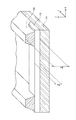
- FIG. FIG. 3 is a schematic cross-sectional view showing a configuration in the AA cross section of FIG.
- A) is a schematic plan view which shows the arrangement
- (b) is a schematic cross section which shows a partial structure in the BB cross section
- FIG. 5 is a schematic cross-sectional view showing a partial configuration in a CC cross section.
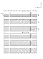
- (A) is a schematic plan view which shows the structure of the bank 804 in the display panel 80 which concerns on a comparative example
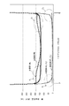
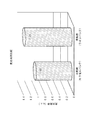
- (b) is a schematic cross section which shows the partial structure in the DD cross section. It is a schematic diagram which shows the surface shape of the organic light emitting layer and hole transport layer in the bank structure which concerns on an Example. It is the figure which compared the luminous efficiency of an Example and a comparative example.
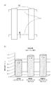
- (A) is a schematic top view which shows the arrangement
- (b) is a figure which shows the relationship between the width
- FIG. 3 is a schematic cross-sectional view showing the configuration of a first bank 104 and a second bank 115.
- FIG. It is a schematic cross section which shows the structure of the bank 304 in the display panel 30 which concerns on Embodiment 2 of this invention.
- (A) is a schematic block diagram which shows the laminated structure of each sub pixel in the display panel 40 which concerns on the modification 1
- (b) is the laminated structure of each sub pixel in the display panel 50 which concerns on the modification 2.
- FIG. It is a schematic block diagram which shows.
- the organic light emitting device is a device in which a plurality of light emitting units are two-dimensionally arranged in a direction along the main surface of a substrate.
- Each of the plurality of light emitting units includes a first electrode, an organic light emitting layer, an intermediate layer, a charge transport layer, and a second electrode in a first direction intersecting with a direction along the main surface of the substrate. And having.
- Organic light-emitting layer is disposed above the first electrode. Note that the first electrode and the organic light emitting layer may be in contact with each other, or another functional layer may be interposed therebetween.
- Organic light emitting layer Arranged above the organic light emitting layer. Note that the organic light emitting layer and the intermediate layer may be in contact with each other, or another functional layer may be interposed therebetween.
- Electrode is disposed above the charge transport layer. Note that the charge transport layer and the second electrode may be in contact with each other, or another functional layer may be interposed therebetween.
- a layer containing fluoride of alkali metal or alkaline earth metal is employed.
- a layer containing an organic material doped with alkali metal or alkaline earth metal is employed.
- each of the plurality of light emitting units is formed to extend in a third direction that intersects the second direction in the second direction, which is one direction in the direction along the main surface of the substrate.
- the first bank is defined by the second bank formed in the third direction and extending in the second direction.
- the first bank and the second bank are each made of an insulating material, and the liquid repellency of the surface portion facing the light emitting portion in the first bank is changed to the liquid repellency of the surface portion facing the light emitting portion in the second bank. Higher than that.
- a layer containing an organic material doped with alkali metal or alkaline earth metal is employed as the charge transport layer, so that high light emission efficiency can be obtained.
- an intermediate layer which is a layer containing an alkali metal or alkaline earth metal fluoride, is disposed between the organic light emitting layer and the charge transport layer, it has a high impurity blocking property. Accordingly, it is possible to effectively block impurities from the organic light emitting layer from entering the charge transport layer. Therefore, deterioration of the charge transport layer can be suppressed and high charge injection properties can be maintained.
- the liquid repellency of the surface portion facing the light emitting portion in the first bank is set higher than the liquid repellency of the surface portion facing the light emitting portion in the second bank. Due to the difference in liquid repellency between the surface portion of the first bank and the surface portion of the second bank, the shape of the layer surface in at least the third direction of the organic layer including the organic light emitting layer is further flattened. The thickness can be made uniform. Therefore, in the organic light emitting device according to this aspect, high luminous efficiency can be realized.
- the emission efficiency can be further improved by obtaining high charge injection properties while suppressing deterioration of the charge transport layer due to impurities.
- the height in the first direction in the first bank is higher than the height in the first direction in the second bank.
- the layer thickness in the region defined by the first bank and the second bank including the organic light emitting layer can be made more uniform. Therefore, in the light emitting device according to this aspect, higher luminous efficiency can be realized.
- an insulating layer is interposed between the substrate and the first electrode, and each height of the first bank and the second bank is equal to that of the insulating layer. It is defined based on the top surface.
- the first bank is higher than the second bank with respect to the height with respect to the upper surface of the insulating layer (the main surface opposite to the substrate), so that the layer thickness can be more uniform. Figured.
- the first bank is stacked on the second bank at the intersection of the first bank and the second bank.
- the first bank and the second bank are not integrally formed, but are formed as different portions.
- the first bank and the second bank may be formed of different materials or may be formed of the same material. It is only necessary to satisfy the above relationship regarding the liquid repellency of the surface portion.
- the height in the first direction in the second bank is in the range of 40% to 70% as compared with the height in the first direction in the first bank. Is in. According to confirmation by the present inventors, if the height ratio between the first bank and the second bank in the first direction is defined as described above, it is desirable from the viewpoint of uniform thickness of the organic layer. Therefore, the organic light emitting device according to this aspect can further improve the light emission efficiency.
- the organic light emitting device in the above configuration, when the light emitting unit and the second bank are viewed in plan from the first direction, when the length in the third direction of the light emitting unit is L P , the third width W 2B two banks are within the scope of 0.20L P ⁇ 0.30L P.
- the width W 2B of the second bank within the range of 0.20 L P to 0.30 L P , the area of the light emitting portion and the layer thickness of the organic layer (including the organic light emitting layer) are made uniform. Can be achieved with high accuracy. Therefore, the organic light emitting device according to this aspect can further improve the light emission efficiency.
- the organic light emitting device in the above configuration, when the light emitting unit and the second bank are viewed in plan from the first direction, when the length in the third direction of the light emitting unit is L P ,
- the width W 2B in the third direction of the two banks is in the range of 0.20 L P to 0.25 L P.
- the third width W 2B of the second bank is made within a range of 0.20 L P ⁇ 0.25 L P, it is possible to improve further the light emission efficiency.
- the first bank and the second bank are integrally formed in the above configuration.
- the light emission efficiency can be improved by defining the liquid repellency between the surface portions as described above.
- the height in the first direction in the first bank is equal to the height in the first direction in the second bank.
- the heights of the first bank and the second bank may be different from each other, or may be the same as in this embodiment. Note that “same” does not necessarily mean completely the same, but allows differences such as variations in manufacturing.
- the liquid repellency of the surface portion in the first bank and the liquid repellency of the surface portion in the second bank are liquid repellency with respect to the ink used in forming the organic light emitting layer. It is sex.
- the liquid repellency at each surface portion of the first bank and the second bank by the liquid repellency with respect to the ink used in forming the organic light emitting layer tail, it is possible to reliably improve the light emission efficiency.
- the intermediate layer is a layer containing sodium fluoride
- the charge transport layer is a layer containing an organic material doped with barium.
- An organic display device includes a display panel and a control drive circuit connected to the display panel.
- the device structure according to any one of the above aspects is employed as the display panel. Since the organic display device according to this aspect employs the device structure according to any one of the aspects described above as the display panel, the same effect as described above can be obtained.
- Embodiment 1 1. Schematic Configuration of Organic EL Display Device 1 A schematic configuration of the organic EL display device 1 according to Embodiment 1 of the present invention will be described with reference to FIGS. 1 and 2.
- the organic EL display device 1 includes a display panel 10 and a drive / control circuit unit 20 connected thereto.
- the display panel 10 is an organic EL panel using an electroluminescence phenomenon of an organic material, and has a plurality of pixels.
- each pixel includes a subpixel 10 a that is a red (R) light-emitting portion, a subpixel 10 b that is a green (G) light-emitting portion, and a subpixel that is a blue (B) light-emitting portion. 10c.
- the plurality of subpixels 10a to 10c are arranged in a matrix (two-dimensional arrangement) in the XY axis direction.
- the drive / control circuit unit 20 is composed of four drive circuits 21 to 24 and a control circuit 25.
- the arrangement relationship between the display panel 10 and the drive / control circuit unit 20 in the organic EL display device 1 is not limited to the form shown in FIG.
- the configuration of the pixels in the display panel 10 is not limited to the form of subpixels (light emitting portions) of three colors of R, G, and B as shown in FIG. 2, and one pixel from the light emitting portions of four or more colors. May be configured.
- the configuration of the display panel 10 will be described with reference to FIG.
- the display panel 10 according to the present embodiment employs a top emission type organic EL panel.
- the display panel 10 has a TFT substrate 100 as a base, and an insulating layer 101 is laminated on the upper surface thereof.
- the insulating layer 101 is formed so that the upper surface in the Z-axis direction is substantially flat.
- a TFT (Thin Film Transistor) layer in the TFT substrate 100 is not shown and is simplified.
- An anode 102 and a hole injection layer 103 are sequentially stacked on the upper surface of the insulating layer 101 in the Z-axis direction.
- the anode 102 and the hole injection layer 103 are provided for each of the subpixels 10a to 10c.
- the hole injection layer 103 can also be formed in a continuous state between the subpixels 10a to 10c.
- a first bank 104 is formed so as to cover the insulating layer 101 and both ends of the hole injection layer 103 in the X-axis direction.
- the first bank 104 is inserted between adjacent subpixels 10a to 10c in the X-axis direction, and defines an opening corresponding to a light emitting region in the X-axis direction.
- a hole transport layer 105 and an organic light emitting layer 106 are laminated in order from the lower side in the Z-axis direction.
- an intermediate layer 107 On the electron transport layer 108 and the top surface of the bank 104, an intermediate layer 107, an electron transport layer 108, a cathode 109, and a sealing layer 110 are sequentially stacked so as to cover them.
- a resin layer 114 is laminated on the upper side of the sealing layer 110 in the Z-axis direction.
- a CF panel in which the color filter layer 112 and the black matrix layer 113 are formed on the main surface of the substrate 111 on the lower side in the Z-axis direction is bonded onto the resin layer 114.
- the resin layer 114 is in intimate contact with the sealing layer 110, the color filter layer 112, and the black matrix layer 113.
- the layer thickness of the organic light emitting layer 106 may differ depending on the emission color.
- the thickness of the organic light emitting layer 106 and T 106a in the sub-pixels 10a, the thickness of the organic light emitting layer 106 and T 106b in the sub-pixel 10b, the organic light emitting layer 106 in the subpixel 10c The layer thickness is T 106c .
- this is not a limitation.
- a plurality of first banks 104 each extending in the Y-axis direction and arranged at intervals from each other in the X-axis direction.
- a plurality of second banks 115 each extending in the X-axis direction and spaced from each other in the Y-axis direction. That is, in this embodiment, a so-called line bank structure is adopted.
- the regions defined by the pair of adjacent first banks 104 and the pair of adjacent second banks 115 become subpixel formation regions 116a to 116c.
- the first bank 104 is interposed between the subpixels 10a to 10c adjacent in the X-axis direction, and the height with respect to the upper surface of the insulating layer 101 is H104 . is there.
- the second bank 115 is interposed between the anode 102 and the hole injection layer 103 adjacent in the Y-axis direction.
- Height of the second bank 115 relative to the upper surface of the insulating layer 101 is H 115.
- the height H 115 of the second bank 115 as compared to the height H 104 of the first bank 104, in the range of 40% to 70%, more particularly in the range of 50% to 55% .
- the liquid repellency of the surface portion 115 a in the second bank 115 is lower than the liquid repellency of the side surface portion 104 a in the first bank 104.
- the liquid repellency of the side surface portion 104 a of the first bank 104 and the liquid repellency of the surface portion 115 a of the second bank 115 are determined with respect to the ink used when forming the hole transport layer 105 and the organic light emitting layer 106. Defined with liquidity.
- the TFT substrate 100 includes a substrate and a TFT layer formed on the upper surface in the Z-axis direction of the substrate.
- the TFT layer is configured to include three electrodes of a gate, a source, and a drain, a semiconductor layer, a passivation film, and the like.
- the substrate serving as the base of the TFT substrate 100 is, for example, a glass substrate, a quartz substrate, a silicon substrate, molybdenum sulfide, copper, zinc, aluminum, stainless steel, magnesium, iron, nickel, gold, silver, or a metal substrate, a gallium arsenide group, or the like. These are formed using a semiconductor substrate, a plastic substrate, or the like.
- thermoplastic resin such as polyethylene, polypropylene, ethylene-propylene copolymer, ethylene-vinyl acetate copolymer (EVA), cyclic polyolefin, modified polyolefin, polyvinyl chloride, polyvinylidene chloride, polystyrene, polyamide, polyimide (PI), Polyamideimide, polycarbonate, poly- (4-methylbenten-1), ionomer, acrylic resin, polymethyl methacrylate, acrylic-styrene copolymer (AS resin), butadiene-styrene copolymer, polio copolymer (EVOH) ), Polyesters such as polyethylene terephthalate (PET), polybutylene terephthalate, polyethylene naphthalate (PEN), precyclohexane terephthalate (PCT), polyethers, polyether ketones Polyethers
- the insulating layer 101 is formed using, for example, an organic compound such as polyimide, polyamide, or acrylic resin material.
- the insulating layer 101 preferably has organic solvent resistance.
- the insulating layer 101 may be subjected to an etching process, a baking process, or the like during the manufacturing process, the insulating layer 101 is formed using a material having high resistance that does not cause excessive deformation or alteration to the process. It is desirable that
- Anode 102 is made of a metal material containing silver (Ag) or aluminum (Al).
- the surface portion thereof preferably has high reflectivity.
- the anode 102 not only a single layer structure made of a metal material as described above, but also a laminate of a metal layer and a transparent conductive layer can be adopted.
- a constituent material of the transparent conductive layer for example, indium tin oxide (ITO), indium zinc oxide (IZO), or the like can be used.
- the hole injection layer 103 may be formed of, for example, an oxide such as silver (Ag), molybdenum (Mo), chromium (Cr), vanadium (V), tungsten (W), nickel (Ni), iridium (Ir), or PEDOT. It is a layer made of a conductive polymer material such as (mixture of polythiophene and polystyrene sulfonic acid).
- an oxide such as silver (Ag), molybdenum (Mo), chromium (Cr), vanadium (V), tungsten (W), nickel (Ni), iridium (Ir), or PEDOT.
- It is a layer made of a conductive polymer material such as (mixture of polythiophene and polystyrene sulfonic acid).
- the organic light emission can be performed stably or by assisting the generation of holes as compared with the case where a conductive polymer material such as PEDOT is used. It has a function of injecting holes into the layer 108 and has a large work function.
- the hole injection layer 103 is made of a transition metal oxide, a plurality of levels can be obtained by taking a plurality of oxidation numbers. As a result, the hole injection becomes easy and the drive voltage is reduced. Can be reduced. In particular, it is desirable to use tungsten oxide (WO X ) from the viewpoint of stably injecting holes and assisting the generation of holes.
- WO X tungsten oxide
- First bank 104 is formed using an organic material such as a resin and has an insulating property.
- organic material used for forming the first bank 104 include acrylic resin, polyimide resin, and novolac type phenol resin.
- the surface of the first bank 104 can be treated with fluorine in order to give the surface water repellency.
- the structure of the first bank 104 not only a single layer structure as shown in FIGS. 3 and 4B but also a multilayer structure of two or more layers can be adopted.
- the above materials can be combined for each layer, and an inorganic material and an organic material can be used for each layer.
- the second bank 115 can be formed using an inorganic insulating material such as SiO 2 (silicon oxide), SiN (silicon nitride), or SiON (silicon oxynitride), or an organic insulating material.
- an inorganic insulating material such as SiO 2 (silicon oxide), SiN (silicon nitride), or SiON (silicon oxynitride), or an organic insulating material.
- organic insulating material examples include, for example, acrylic resins, polyimide resins, siloxane resins, phenol resins, and the like.
- Hole transport layer 105 is formed using a polymer compound having no hydrophilic group.
- a polymer compound having no hydrophilic group for example, polyfluorene or a derivative thereof, or a polymer compound such as polyarylamine or a derivative thereof that does not have a hydrophilic group can be used.
- Organic light emitting layer 106 has a function of emitting light by generating an excited state by injecting and recombining holes and electrons.
- As a material used for forming the organic light emitting layer 106 it is necessary to use a light emitting organic material that can be formed by a wet printing method.
- the oxinoid compound, perylene compound, coumarin compound, azacoumarin compound, oxazole compound, oxadiazole compound, perinone compound, pyrrolopyrrole described in the patent publication (Japan / JP-A-5-163488) Compound, naphthalene compound, anthracene compound, fluorene compound, fluoranthene compound, tetracene compound, pyrene compound, coronene compound, quinolone compound and azaquinolone compound, pyrazoline derivative and pyrazolone derivative, rhodamine compound, chrysene compound, phenanthrene compound, cyclopentadiene compound, stilbene compound , Diphenylquinone compound, styryl compound, butadiene compound, dicyanomethylenepyran compound, dicyanomethylenethiopyran compound, fluoro Cein compounds, pyrylium compounds, thiapyrylium
- the intermediate layer 107 includes an alkali metal or alkaline earth metal fluoride.
- NaF sodium fluoride
- Electron transport layer 108 has a function of transporting electrons injected from the cathode 118 to the organic light emitting layer 106, and is made of, for example, an organic material doped with alkali metal or alkaline earth metal.
- Ba (barium) is doped with respect to a ⁇ -electron-based low-molecular organic material such as an oxadiazole derivative (OXD), a triazole derivative (TAZ), or a phenanthroline derivative (BCP, Bphen). Being done.
- the doped metal in the structure of the electron transport layer 108 is a low work function metal such as Li (lithium), Ca (calcium), Ce (cesium), Na (sodium), and Rb (rubidium).
- low work function metal salts such as lithium fluoride, low work function metal oxides such as barium oxide, and low work function metal organic complexes such as lithium quinolinol.
- the concentration of the doped metal is preferably in the range of 5 wt% to 40 wt%, for example.
- Cathode 109 is formed using, for example, indium tin oxide (ITO) or indium zinc oxide (IZO).
- ITO indium tin oxide
- IZO indium zinc oxide
- permeability shall be 80 [%] or more.
- the sealing layer 110 has a function of suppressing exposure of an organic layer such as the organic light emitting layer 106 to moisture or exposure to air.
- an organic layer such as the organic light emitting layer 106
- silicon nitride (SiN) silicon oxynitride (SiON) It is formed using materials such as.
- a sealing resin layer made of a resin material such as an acrylic resin or a silicone resin may be provided over a layer formed using a material such as silicon nitride (SiN) or silicon oxynitride (SiON).
- the sealing layer 110 needs to be formed of a light transmissive material.
- the substrate 111 is, for example, a glass substrate, a quartz substrate, a silicon substrate, molybdenum sulfide, copper, zinc, aluminum, stainless steel, magnesium, iron, nickel, gold, silver, or other metal substrate, gallium arsenide base, like the substrate 100 described above. These are formed using a semiconductor substrate such as a plastic substrate. As for the substrate 111, when a plastic substrate is employed, either a thermoplastic resin or a thermosetting resin may be used.
- Color filter layer 112 is made of a known material that selectively transmits visible light in the wavelength range of each color of red (R), green (G), and blue (B). For example, it is formed based on an acrylic resin.
- Black matrix layer 113 is made of, for example, an ultraviolet curable resin material containing a black pigment having excellent light absorption and light shielding properties.
- Specific examples of the ultraviolet curable resin material include an acrylic resin.
- Resin layer 114 is formed from a transparent resin material, for example, an epoxy resin material. However, as a constituent material of the resin portion 130, a silicone resin or the like can be used in addition to this.
- Example An example is the display panel 10 according to the first embodiment shown in FIG. Of the subpixels 10a to 10c, the measurement was performed on the subpixel 10a having the thickest organic light emitting layer 106, ie, T106a .
- the size in the X-axis direction of the subpixel 10a is 65 ⁇ m, and the size in the Y-axis direction is 250 ⁇ m.
- the contact angle (against anisole) at the side surface portion 104a of the first bank 104 is 45 ° to 60 °, whereas the contact angle (against anisole) at the surface portion 115a of the second bank 115 is 5 ° or less.
- the display panel 80 according to the comparative example employs a so-called pixel bank structure, and the bank 804 extends in the Y-axis direction and the first bank element 804a extends in the X-axis direction.
- the two bank elements 804b are integrally formed.
- Recesses defined by the surroundings of the bank 804 are subpixel formation regions 816a to 816c.
- the height of the top surface of the bank 804 is the same in the entire display region, and the liquid repellent properties of the side surface portions 804aa and 804ba facing the opening.
- the sex is also the same.
- FIG. 5B only the insulating layer 801, the anode 802, the hole injection layer 803, and the bank 804 are extracted and illustrated. However, the components other than the bank 804 are the same as those in the above embodiment.
- the size of the sub-pixel in plan view is the same as that in the above embodiment.
- FIG. 6 is a diagram showing surface shapes in the Y-axis direction of the applied and dried hole injection layer (HTL) and organic light emitting layer (EML) for each of Examples and Comparative Examples.
- a broken line in the figure shows a comparative example, and a practical example shows an example.
- the hole transport layer (HTL) 105 has a substantially flat surface shape from the end of the subpixel in the Y-axis direction.
- the flatness is reduced at both ends in the Y-axis direction. Specifically, the layer surface rises upward in the Z-axis direction as it approaches the side surface of the second bank element 804b of the bank 804.
- the contact angle of the side surface portion 104a of the base 1 bank 104 is 45 ° to 60 °, whereas the contact angle of the surface portion 115a of the second bank 115 is set to 5 ° or less. This is desirable from the viewpoint of ensuring surface flatness in the organic layer.
- the organic light emitting layer (EML) 106 according to the example also has a substantially flat surface shape from end to end of the subpixel in the Y-axis direction.
- the flatness is lowered at both ends in the Y-axis direction. Specifically, the layer surface rises upward in the Z-axis direction as it approaches the side surface of the second bank element 804b of the bank 804. In the case of the organic light emitting layer, the degree of the bulge of the surface at the end of the subpixel is larger than in the case of the hole transport layer.
- the liquid repellency of the surface portion 115 a in the second bank 115 is made lower than the liquid repellency of the side surface portion 104 a in the first bank 104, and the height H 115 of the second bank 115 is set to be lower than that of the first bank 104.
- the height H 104 was lowered embodiment, as compared with the comparative example, it was possible to flatten the surface shape of the organic light emitting layer 106 and the hole-transporting layer 105. Therefore, in the display panel 10 according to the example, it is considered that the thicknesses of the organic light emitting layer 106 and the hole transport layer 105 in the display region can be made uniform.
- the surface shapes of the organic light emitting layer 106 and the hole transport layer 105 were measured.
- the organic layer formed in the region defined by the first bank 104 and the second bank 115 has similar results. Presumed to be.
- Luminous Efficiency measurement results of luminous efficiency in each of the display panels 10 and 80 of the above examples and comparative examples will be described with reference to FIG.
- the light emission efficiency in the display panel 80 according to the comparative example is set to 100, and the light emission efficiency in the display panel 10 according to the example is shown in comparison with the light emission efficiency.
- the light emission efficiency is improved by 29% compared to the display panel 80 according to the comparative example.
- this is because the relationship between the side surface portion 104a of the first bank 104 and the surface portion 115a of the second bank 115, and the height H 104 of the first bank 104 and the height H 115 of the second bank 115 are as follows . This is considered to be caused by the relationship.
- the width of the second bank 115 The relationship between the width of the second bank 115 and the light emission efficiency will be described with reference to FIG.
- FIG. 8A a display panel prepared with the following two levels for the width W 2B of the second bank 115 was manufactured, and each luminous efficiency was measured. About a measurement result, it shows in FIG.8 (b) by the ratio with respect to the said comparative example.
- Example 1 The width W 2B of the second bank 115 is set to 70 ⁇ m, and other configurations are the same as those of the display panel 1.
- the size of the subpixels 10a to 10c is 65 ⁇ m ⁇ 250 ⁇ m as described above. Therefore, the ratio of the width W 2B of the second bank 115 to the longitudinal size of the subpixels 10a to 10c is about 28%.
- the width W 2B of the second bank 115 is set to 55 ⁇ m, and other configurations are the same as those of the display panel 1.
- the size of the subpixels 10a to 10c is 65 ⁇ m ⁇ 250 ⁇ m as described above, and the ratio of the width W 2B of the second bank 115 to the longitudinal size of the subpixels 10a to 10c is about 22%.
- the display panel according to Example 1 was able to achieve a light emission efficiency 29% higher than that of the display panel according to the comparative example.
- the display panel according to Example 2 in which the width W 2B of the second bank 115 was further narrowed was able to achieve a light emission efficiency that was 33% higher than that of the display panel according to the comparative example.
- the width W 2B of the second bank 115 is within the range of 20% to 30%, and more preferably within the range of 20% to 25%, in the ratio to the longitudinal size of the subpixels 10a to 10c. This is desirable from the viewpoint of realizing high luminous efficiency.
- the second bank 115 plays a role of covering the edge portions of the anode 102 and the hole injection layer 103, it is desirable to reduce the extra width W 2B in consideration of a margin at the time of manufacturing. Absent.
- Second Bank 115 The height of the second bank 115 will be described with reference to FIG.
- the second bank 115 extending in the X-axis direction is formed on the insulating layer 101, and the Y-axis direction is covered so as to cover a part thereon.
- a first bank 104 extending in the direction is formed.
- the height to the top surface of the first bank 104 is H 1B
- the height to the top surface (upper surface in the Z-axis direction) of the second bank 115 is H 2B.
- the relationship of H 2B / H 1B ⁇ 54% is satisfied.
- the ratio between the height H 1B and the height H 2B is not limited to this.
- the height H 2B of the second bank 115 may be substantially 100% with respect to the height H 1B of the first bank 104 except for the intersection of the first bank 104 and the second bank 115.
- the height ratio H 2B / H 1B is set to 40% or more in consideration of planarization of the surface in the organic layer. It is desirable to be within the range of 70%.
- Embodiment 2 The configuration of the organic EL display device according to Embodiment 2 of the present invention will be described with reference to FIG.
- the bank 304 in the display panel 30 which is a structural difference from the organic EL display device 1 according to the first embodiment is mainly illustrated.
- Other configurations are the same as those in the first embodiment.
- the anode 302 and the hole injection layer 303 are sequentially stacked on the upper surface of the insulating layer 301 in the Z-axis direction.
- the anode 302 and the hole injection layer 303 are formed separately for each subpixel.
- a bank 304 is laminated so as to cover a part (exposed portion) of the upper surface in the Z-axis direction of the insulating layer 301 and an edge portion of the upper surface in the Z-axis direction of the hole injection layer 303.
- a first bank element 304a extending in the Y-axis direction and a second bank element 304b extending in the X-axis direction are integrally formed.
- the first bank element 304a and the second bank element 304b in the bank 304 are formed using the same bank material, and the upper surface in the Z-axis direction is formed flush.
- the liquid repellency of the side surface portion 304ba of the second bank element 304b is set lower than the liquid repellency of the side surface portion 304aa of the first bank element 304a.
- the contact angle of the side surface portion 304aa of the first bank element 304a is 45 ° to 60 °, while the contact angle of the side surface portion 304ba of the second bank element 304b is 5 ° or less.
- both liquid repellency of the side surface portion 304ba of the second bank element 304b and the side surface portion 304aa of the first bank element 304a is applied and formed in the opening surrounded by the bank 304. It is liquid repellent with respect to an organic layer (especially organic light emitting layer).
- the side surface portion 304ba of the second bank element 304b and the side surface portion 304aa of the first bank element 304a are both highly repellent to the ink with respect to the exposed surface 303a of the hole injection layer 303 whose surface is lyophilic. It has liquidity.
- the display panel 30 according to the present embodiment employs a so-called pixel bank structure, but the liquid repellency of the side surface portion 304aa of the first bank element 304a and the liquid repellency of the side surface portion 304ba of the second bank element 304b.
- pixel bank structure the liquid repellency of the side surface portion 304aa of the first bank element 304a and the liquid repellency of the side surface portion 304ba of the second bank element 304b.
- the configuration in which the intermediate layer is interposed between the organic light emitting layer and the electron transport layer is the same as that in the first embodiment, it is possible to effectively block impurities from entering the electron transport layer. .
- the display panel 30 according to the present embodiment high storage stability can be realized, and the deterioration of the electron transport layer is suppressed, similarly to the display panel 10 according to the first embodiment. Electron injection property can be maintained.
- Modification 1 A configuration of the display panel 40 according to Modification 1 will be described with reference to FIG. In FIG. 11A, only the laminated structure of the light emitting portions in the display panel 40 is schematically shown.
- an organic light emitting layer 406 is disposed between the anode 402 and the cathode 409. Between the anode 402 and the organic light emitting layer 406, a hole injection layer 403 and a hole transport layer 405 are sequentially stacked from the anode 402 side.
- a layer made of NaF is adopted as an example of the intermediate layer 107, but in this modification, a layer made of a fluoride of an alkali metal or alkaline earth metal excluding Na is used. Specifically, a layer made of a fluoride such as Li is employed as the intermediate layer 407.
- the intermediate layer 407 is interposed between the organic light emitting layer tail 406 and the electron transport layer 408, and the intermediate layer 407 has a low work function and a high electron injection property.
- the display panel 10 according to the first embodiment is formed, high storage stability can be realized, deterioration of the electron transport layer is suppressed, and high electrons are formed. Injectability can be maintained.
- an organic light emitting layer 506 is disposed between the anode 502 and the cathode 509, and the anode 502 side is disposed between the anode 502 and the organic light emitting layer 506.
- a hole injection layer 503 and a hole transport layer 505 that are sequentially stacked are inserted.
- the configuration up to here is the same as in the first embodiment and the first modification.
- an intermediate layer 507, a second intermediate layer 517, and an electron transport layer 508, which are sequentially stacked from the organic light emitting layer 506 side, are interposed between the organic light emitting layer 506 and the cathode 509. Has been.
- the intermediate layer 507 is a layer made of a fluoride of an alkali metal or an alkaline earth metal (for example, sodium) as in the first embodiment and the first modification.
- the second intermediate layer 517 a metal having a function of decomposing a bond between an alkali metal or an alkaline earth metal and fluorine with respect to an alkali metal or alkaline earth metal fluoride contained in the intermediate layer 507 is used. It is a layer that contains. Specifically, the second intermediate layer 517 is made of an alkali metal or an alkaline earth metal. More specifically, for example, it is a layer made of barium (Ba).
- Alkali metal or alkaline earth metal fluoride (for example, NaF) in the intermediate layer 507 has high electrical insulation. For this reason, it is thought that the electron injection property from the electron carrying layer 508 to the organic light emitting layer 506 is inhibited. For this reason, by inserting a second intermediate layer 517 made of an alkali metal or an alkaline earth metal between the intermediate layer 507 and the electron transport layer 508 as in the second modification, The bond between the alkali metal or alkaline earth metal and fluorine in the intermediate layer 507 can be decomposed. Accordingly, alkali metal or alkaline earth metal (for example, Na) in the intermediate layer 507 is liberated, and the electron injection property from the electron transport layer 508 to the organic light emitting layer 506 can be maintained high.
- alkali metal or alkaline earth metal fluoride for example, NaF
- the layer thickness of the second intermediate layer 517 be in the range of 3% to 25% with respect to the layer thickness of the intermediate layer 507.
- the layer thickness of the intermediate layer 507 is desirably about 1 nm to 10 nm, and the layer thickness of the second intermediate layer 517 is desirably about 0.1 nm to 1 nm.
- the doped metal in the electron transport layer 508 and the metal constituting the second intermediate layer 517 are the same kind of metal. This is in consideration of ease of manufacture. In particular, it is desirable to use barium as the metal. This is because the cost can be reduced by using a versatile metal such as barium.
- Embodiments 1 and 2 and Modifications 1 and 2 the display panels 10, 30, 40, and 50, which are organic EL panels, are employed as an example of the organic light emitting device, but the present invention is limited thereto. It is not a thing. For example, the same effect as described above can be obtained by applying the configuration of the present invention to organic EL lighting or the like.
- the active matrix display panels 10, 30, 40, and 50 are used.
- the present invention is not limited to this.
- the present invention can be applied to a passive matrix display panel.
- one pixel is composed of a combination of three subpixels 10a to 10c each having a rectangular shape in plan view.
- the invention is not limited to this.
- the planar view shape of each subpixel may be a triangle, a hexagon, or an octagon.
- it can also be made into a honeycomb shape as a whole.
- the first bank may be meandered in a crank shape in plan view.
- the number of subpixels constituting one pixel may be four or more.
- a plurality of subpixels constituting one pixel may emit light of different colors, or a part thereof may emit light of the same color.
- a wiring layer (bus bar wiring) connected to the cathode may be provided between adjacent pixels in the X-axis direction in FIG.
- the intermediate layers 107, 407, 507 or the second intermediate layer are provided between the organic light emitting layers 106, 406, 506 and the electron transport layers 108, 408, 508.
- the present invention is not limited to this.
- an intermediate layer having a barrier property may be interposed between the organic light emitting layer and the electron transport layer. Even in this case, it is considered that the intrusion of impurities from the organic light emitting layer to the electron transport layer can be suppressed, and the decrease in hole injection property can be suppressed.
- the constituent material of the intermediate layers 107, 407, and 507 is not limited to NaF, and the constituent material of the second intermediate layer 517 is not limited to Ba.
- the intermediate layer may be made of an alkali metal or alkaline earth metal fluoride, and may contain impurities.
- the second intermediate layer only needs to be made of an alkali metal or an alkaline earth metal, and in the adjacent charge transport layer (in Embodiments 1 and 2 and Modifications 1 and 2, the electron transport layer 108, If it is the same kind as the doped metal in 408,508), it is more desirable.
- the so-called top emission type structure is adopted, but a bottom emission type structure can also be adopted. Further, the arrangement relationship between the anodes 102, 302, 402, 502 and the cathodes 109, 409, 509 in the Z-axis direction can be reversed. Even in this case, a top emission type structure and a bottom emission type structure can be selectively employed as appropriate.
- the present invention is useful for realizing an organic light emitting device and an organic display device having high luminous efficiency.
- Subpixel 20. Drive / control circuit section 21-24.
Landscapes
- Physics & Mathematics (AREA)
- Optics & Photonics (AREA)
- Engineering & Computer Science (AREA)
- Microelectronics & Electronic Packaging (AREA)
- Electroluminescent Light Sources (AREA)
Abstract
Description
本発明の一態様に係る有機発光デバイスは、複数の発光部が基板の主面に沿った方向に二次元配置されてなるデバイスである。そして、複数の発光部の各々は、基板の主面に沿った方向に対して交差する第1方向において、第1電極と、有機発光層と、中間層と、電荷輸送層と、第2電極と、を有する。
1.有機EL表示装置1の概略構成
本発明の実施の形態1に係る有機EL表示装置1の概略構成について、図1および図2を用い説明する。
表示パネル10の構成について、図3を用い説明する。本実施の形態に係る表示パネル10は、一例としてトップエミッション型の有機ELパネルを採用する。
次に、表示パネル10におけるバンク104,115の配置形態について、図4を用い説明する。
(1)TFT基板100
TFT基板100は、基板と、当該基板のZ軸方向上面に形成されたTFT層とから構成されている。TFT層については、図示を省略しているが、ゲート、ソース、ドレインの3電極と、半導体層、パッシベーション膜などを含み構成されている。
絶縁層101は、例えば、ポリイミド、ポリアミド、アクリル系樹脂材料などの有機化合物を用い形成されている。ここで、絶縁層101は、有機溶剤耐性を有することが好ましい。
アノード102は、銀(Ag)またはアルミニウム(Al)を含む金属材料から構成されている。トップエミッション型の本実施の形態に係る表示パネル10の場合には、その表面部が高い反射性を有することが好ましい。
ホール注入層103は、例えば、銀(Ag)、モリブデン(Mo)、クロム(Cr)、バナジウム(V)、タングステン(W)、ニッケル(Ni)、イリジウム(Ir)などの酸化物、あるいは、PEDOT(ポリチオフェンとポリスチレンスルホン酸との混合物)などの導電性ポリマー材料からなる層である。
第1バンク104は、樹脂等の有機材料を用い形成されており絶縁性を有する。第1バンク104の形成に用いる有機材料の例としては、アクリル系樹脂、ポリイミド系樹脂、ノボラック型フェノール樹脂等があげられる。第1バンク104は、表面に撥水性をもたせるために、表面をフッ素処理することもできる。
第2バンク115は、SiO2(酸化シリコン)、SiN(窒化シリコン)、SiON(酸窒化シリコン)などの無機絶縁材料や、有機絶縁材料などを用い形成することができる。
ホール輸送層105は、親水基を備えない高分子化合物を用い形成されている。例えば、ポリフルオレンやその誘導体、あるいはポリアリールアミンやその誘導体などの高分子化合物であって、親水基を備えないものなどを用いることができる。
有機発光層106は、ホールと電子とが注入され再結合されることにより励起状態が生成され発光する機能を有する。有機発光層106の形成に用いる材料は、湿式印刷法を用い製膜できる発光性の有機材料を用いることが必要である。
中間層107は、アルカリ金属若しくはアルカリ土類金属のフッ化物を含み構成されている。本実施の形態では、例えば、NaF(フッ化ナトリウム)を用い形成されている。
電子輸送層108は、カソード118から注入された電子を有機発光層106へ輸送する機能を有し、例えば、アルカリ金属若しくはアルカリ土類金属をドープしてなる有機材料から構成されている。本実施の形態では、例えば、オキサジアゾール誘導体(OXD)、トリアゾール誘導体(TAZ)、フェナンスロリン誘導体(BCP、Bphen)などのπ電子系低分子有機材料に対して、Ba(バリウム)がドープされてなる。
カソード109は、例えば、酸化インジウムスズ(ITO)若しくは酸化インジウム亜鉛(IZO)などを用い形成される。本実施の形態のように、トップエミッション型の本実施の形態に係る表示パネル10の場合においては、光透過性の材料で形成されることが必要となる。光透過性については、透過率が80[%]以上とすることが好ましい。
封止層110は、有機発光層106などの有機層が水分に晒されたり、空気に晒されたりすることを抑制する機能を有し、例えば、窒化シリコン(SiN)、酸窒化シリコン(SiON)などの材料を用い形成される。また、窒化シリコン(SiN)、酸窒化シリコン(SiON)などの材料を用い形成された層の上に、アクリル樹脂、シリコーン樹脂などの樹脂材料からなる封止樹脂層を設けてもよい。
基板111は、上記基板100と同様に、例えば、ガラス基板、石英基板、シリコン基板、硫化モリブデン、銅、亜鉛、アルミニウム、ステンレス、マグネシウム、鉄、ニッケル、金、銀などの金属基板、ガリウム砒素基などの半導体基板、プラスチック基板等を用い形成されている。基板111についても、プラスチック基板を採用する場合には、熱可塑性樹脂、熱硬化性樹脂いずれの樹脂を用いてもよい。
カラーフィルタ層112としては、赤色(R)、緑色(G)、青色(B)の各色の波長域の可視光を選択的に透過する、公知の材料から構成される。例えば、アクリル樹脂をベースに形成されている。
ブラックマトリクス層113は、例えば、光吸収性および遮光性に優れる黒色顔料を含む紫外線硬化樹脂材料から構成されている。具体的な紫外線硬化樹脂材料としては、例えば、アクリル樹脂等がある。
樹脂層114は、透明樹脂材料、例えば、エポキシ系樹脂材料から形成されている。ただし、樹脂部130の構成材料としては、これ以外にもシリコーン系樹脂などを用いることもできる。
有機発光層106およびホール輸送層105の各表面形状の測定結果について、図5および図6を用い説明する。
実施例は、図3などで示した上記実施の形態1に係る表示パネル10である。なお、サブピクセル10a~10cのうち、有機発光層106の層厚がT106aと最も厚いサブピクセル10aについて測定を実施した。
図5(a)に示すように、比較例に係る表示パネル80では、所謂、ピクセルバンク構造を採用し、バンク804がY軸方向に延伸する第1バンク要素804aとX軸方向に延伸する第2バンク要素804bとが一体に形成されてなる。そして、バンク804の囲繞により規定された各凹部がサブピクセル形成領域816a~816cである。
図6は、実施例および比較例の各々について、塗布・乾燥したホール注入層(HTL)および有機発光層(EML)のY軸方向における表面形状を示す図である。図中における破線で示すのが比較例であり、実践で示すのが実施例である。
図6に示すように、実施例に係るホール輸送層(HTL)105では、Y軸方向におけるサブピクセルの端から端まで略平坦な表面形状となっている。
図6に示すように、実施例に係る有機発光層(EML)106でも、Y軸方向におけるサブピクセルの端から端まで略平坦な表面形状となっている。
次に、上記実施例および比較例の各表示パネル10,80での発光効率の測定結果について、図7を用い説明する。図7では、比較例に係る表示パネル80における発光効率を100とし、それとの対比において実施例に係る表示パネル10における発光効率を示している。
第2バンク115の幅と発光効率との関係について、図8を用い説明する。
第2バンク115の幅W2B=70μmとし、他の構成は上記表示パネル1と同様である。なお、サブピクセル10a~10cのサイズについては、上記同様に65μm×250μmである。よって、サブピクセル10a~10cの長手方向サイズに対する第2バンク115の幅W2Bの比率は、約28%である。
第2バンク115の幅W2B=55μmとし、他の構成は上記表示パネル1と同様である。なお、サブピクセル10a~10cのサイズについては、上記同様に65μm×250μmであり、サブピクセル10a~10cの長手方向サイズに対する第2バンク115の幅W2Bの比率は、約22%である。
比較例については、上記同様に、所謂、ピクセルバンク構造を採用し、他の構成については、実施例1,2と同様である。なお、比較例におけるバンク側面部の撥液性については、上記同様に、全ての領域で同一としている。
図8(b)に示すように、実施例1に係る表示パネルでは、比較例に係る表示パネルに比べて、29%高い発光効率を実現することができた。
第2バンク115の高さについて、図9を用い説明する。
本発明の実施の形態2に係る有機EL表示装置の構成について、図10を用い説明する。なお、図10では、上記実施の形態1に係る有機EL表示装置1との構成上の差異部分である表示パネル30におけるバンク304を主に図示する。その他の構成については、上記実施の形態1と同様である。
変形例1に係る表示パネル40の構成について、図11(a)を用い説明する。なお、図11(a)では、表示パネル40における発光部の積層構造だけを模式的に表している。
変形例2に係る表示パネル50の構成について、図11(b)を用い説明する。なお、図11(b)では、表示パネル50における発光部の積層構造だけを模式的に表している。
上記実施の形態1,2および変形例1,2では、有機発光デバイスの一例として、有機ELパネルである表示パネル10,30,40,50を採用したが、本発明は、これに限定を受けるものではない。例えば、有機EL照明等に本発明の構成を適用することでも上記同様の効果を得ることができる。
10,30,40,50.表示パネル
10a,10b,10c.サブピクセル
20.駆動・制御回路部
21~24.駆動回路
25.制御回路
100.TFT基板
101,301.絶縁層
102,302,402,502.アノード
103,303,403,503.ホール注入層
104.第1バンク
105,405,505.ホール輸送層
106,406,506.有機発光層
107,407,507.中間層
108,408,508.電子輸送層
109,409,509.カソード
110.封止層
111.基板
112.カラーフィルタ層
113.ブラックマトリクス層
114.樹脂層
115.第2バンク
116a,116b,116c.サブピクセル形成領域
304.バンク
304a.第1バンク要素
304b.第2バンク要素
517.第2中間層
Claims (12)
- 複数の発光部が基板の主面に沿った方向に二次元配置されてなる有機発光デバイスであって、
前記複数の発光部の各々は、前記基板の主面に沿った方向に対して交差する第1方向において、
前記基板の上方に配置された第1電極と、
前記第1電極の上方に配置された有機発光層と、
前記有機発光層の上方に配置された中間層と、
前記中間層上に配置された電荷輸送層と、
前記電荷輸送層の上方に配置された第2電極と、
を有し構成されており、
前記中間層は、アルカリ金属若しくはアルカリ土類金属のフッ化物を含み、
前記電荷輸送層は、アルカリ金属若しくはアルカリ土類金属がドープされてなる有機材料を含む層であり、
前記複数の発光部の各々は、前記基板の主面に沿った方向における一の方向である第2方向において、前記第2方向に対して交差する第3方向に延伸形成された第1バンクにより規定され、前記第3方向において、前記第2方向に延伸形成された第2バンクにより規定されており、
前記第1バンクおよび前記第2バンクは、それぞれ絶縁性材料からなるとともに、前記第1バンクにおける前記発光部に面する面部の撥液性が、前記第2バンクにおける前記発光部に面する面部の撥液性に比べて高い
ことを特徴とする有機発光デバイス。 - 前記第1バンクにおける前記第1方向での高さは、前記第2バンクにおける前記第1方向での高さに比べて高い
請求項1記載の有機発光デバイス。 - 前記基板と前記第1電極との間には、絶縁層が介挿されており、
前記第1バンクおよび前記第2バンクの各高さは、前記絶縁層の上面を基準に規定されている
請求項2記載の有機発光デバイス。 - 前記第1バンクと前記第2バンクとの交差部分においては、前記第2バンク上に前記第1バンクが積層されている
請求項2または請求項3記載の有機発光デバイス。 - 前記第2バンクにおける前記第1方向での高さは、前記第1バンクにおける前記第1方向での高さに比べて40%~70%の範囲内にある
請求項2から請求項4の何れか記載の有機発光デバイス。 - 前記第1方向から前記発光部および前記第2バンクを平面視する場合に、
前記発光部における前記第3方向の長さをLPとするとき、
前記第2バンクの前記第3方向の幅W2Bは、0.20LP~0.30LPの範囲内にある
請求項2から請求項5の何れか記載の有機発光デバイス。 - 前記第1方向から前記発光部および前記第2バンクを平面視する場合に、
前記発光部における前記第3方向の長さをLPとするとき、
前記第2バンクの前記第3方向の幅W2Bは、0.20LP~0.25LPの範囲内にある
請求項2から請求項5の何れか記載の有機発光デバイス。 - 前記第1バンクと前記第2バンクとは、一体形成されている
請求項1記載の有機発光デバイス。 - 前記第1バンクにおける前記第1方向での高さと、前記第2バンクにおける前記第1方向での高さとは等しい
請求項8記載の有機発光デバイス。 - 前記第1バンクにおける前記面部の撥液性、および前記第2バンクにおける前記面部の撥液性は、前記有機発光層の形成に際して用いられるインクに対する撥液性である
請求項1から請求項9の何れか記載の有機発光デバイス。 - 前記中間層は、ナトリウムのフッ化物を含む層であり、
前記電荷輸送層は、バリウムがドープされてなる有機材料を含む層である
請求項1から請求項10の何れか記載の有機発光デバイス。 - 表示パネルと、
前記表示パネルに接続された制御駆動回路と、
を備え、
前記表示パネルとして、請求項1から請求項11の何れかのデバイス構造が採用されている
ことを特徴とする有機表示装置。
Priority Applications (2)
| Application Number | Priority Date | Filing Date | Title |
|---|---|---|---|
| JP2016503966A JP6332769B2 (ja) | 2014-02-21 | 2015-02-13 | 有機発光デバイスと有機表示装置 |
| US15/117,546 US9786726B2 (en) | 2014-02-21 | 2015-02-13 | Organic light-emitting device and organic display device |
Applications Claiming Priority (2)
| Application Number | Priority Date | Filing Date | Title |
|---|---|---|---|
| JP2014-031299 | 2014-02-21 | ||
| JP2014031299 | 2014-02-21 |
Publications (1)
| Publication Number | Publication Date |
|---|---|
| WO2015125448A1 true WO2015125448A1 (ja) | 2015-08-27 |
Family
ID=53877971
Family Applications (1)
| Application Number | Title | Priority Date | Filing Date |
|---|---|---|---|
| PCT/JP2015/000676 Ceased WO2015125448A1 (ja) | 2014-02-21 | 2015-02-13 | 有機発光デバイスと有機表示装置 |
Country Status (3)
| Country | Link |
|---|---|
| US (1) | US9786726B2 (ja) |
| JP (1) | JP6332769B2 (ja) |
| WO (1) | WO2015125448A1 (ja) |
Cited By (3)
| Publication number | Priority date | Publication date | Assignee | Title |
|---|---|---|---|---|
| US9730475B1 (en) | 2016-12-12 | 2017-08-15 | Anita Tomkoria | Brassiere accessory for improving posture |
| JP2020537281A (ja) * | 2017-10-13 | 2020-12-17 | 京東方科技集團股▲ふん▼有限公司Boe Technology Group Co.,Ltd. | アレイ基板、表示パネル、表示装置及びその製造方法 |
| US11508928B2 (en) | 2019-11-29 | 2022-11-22 | Joled Inc. | Self-luminous element and self-luminous display panel |
Families Citing this family (2)
| Publication number | Priority date | Publication date | Assignee | Title |
|---|---|---|---|---|
| JP6688701B2 (ja) * | 2016-08-10 | 2020-04-28 | 株式会社Joled | 有機el表示パネル、及び有機el表示パネルの製造方法 |
| JP6807350B2 (ja) * | 2018-05-30 | 2021-01-06 | 株式会社Joled | 有機el表示パネル、有機el表示装置、及び、有機el表示パネルの製造方法 |
Citations (6)
| Publication number | Priority date | Publication date | Assignee | Title |
|---|---|---|---|---|
| JP2001102175A (ja) * | 1999-09-29 | 2001-04-13 | Junji Kido | 有機エレクトロルミネッセント素子、有機エレクトロルミネッセント素子群及びその発光スペクトルの制御方法 |
| JP2007095521A (ja) * | 2005-09-29 | 2007-04-12 | Toppan Printing Co Ltd | 有機エレクトロルミネッセンス素子の製造方法 |
| JP2009200049A (ja) * | 2007-05-28 | 2009-09-03 | Panasonic Corp | 有機elデバイス |
| JP2013033872A (ja) * | 2011-08-03 | 2013-02-14 | Sumitomo Chemical Co Ltd | 有機エレクトロルミネッセンス素子 |
| JP2013074085A (ja) * | 2011-09-28 | 2013-04-22 | Konica Minolta Holdings Inc | 有機エレクトロルミネッセンス素子 |
| JP2013077430A (ja) * | 2011-09-30 | 2013-04-25 | Panasonic Corp | インクジェット装置 |
Family Cites Families (8)
| Publication number | Priority date | Publication date | Assignee | Title |
|---|---|---|---|---|
| US5443922A (en) | 1991-11-07 | 1995-08-22 | Konica Corporation | Organic thin film electroluminescence element |
| JPH05163488A (ja) | 1991-12-17 | 1993-06-29 | Konica Corp | 有機薄膜エレクトロルミネッセンス素子 |
| TW474114B (en) | 1999-09-29 | 2002-01-21 | Junji Kido | Organic electroluminescent device, organic electroluminescent device assembly and method of controlling the emission spectrum in the device |
| JP4872288B2 (ja) | 2005-09-22 | 2012-02-08 | 凸版印刷株式会社 | 有機el素子及びその製造方法 |
| US20070210705A1 (en) | 2006-03-09 | 2007-09-13 | Hajime Yokoi | Organic electroluminescent element and manufacturing method of an organic electroluminescent element and a display |
| JP4882508B2 (ja) | 2006-05-23 | 2012-02-22 | 凸版印刷株式会社 | 有機エレクトロルミネッセンス素子の製造方法 |
| WO2013018251A1 (ja) * | 2011-08-03 | 2013-02-07 | パナソニック株式会社 | 有機発光素子 |
| US9171894B2 (en) * | 2012-05-31 | 2015-10-27 | Joled Inc. | Organic EL element, organic EL panel, organic EL light-emitting apparatus and organic EL display apparatus |
-
2015
- 2015-02-13 WO PCT/JP2015/000676 patent/WO2015125448A1/ja not_active Ceased
- 2015-02-13 US US15/117,546 patent/US9786726B2/en active Active
- 2015-02-13 JP JP2016503966A patent/JP6332769B2/ja active Active
Patent Citations (6)
| Publication number | Priority date | Publication date | Assignee | Title |
|---|---|---|---|---|
| JP2001102175A (ja) * | 1999-09-29 | 2001-04-13 | Junji Kido | 有機エレクトロルミネッセント素子、有機エレクトロルミネッセント素子群及びその発光スペクトルの制御方法 |
| JP2007095521A (ja) * | 2005-09-29 | 2007-04-12 | Toppan Printing Co Ltd | 有機エレクトロルミネッセンス素子の製造方法 |
| JP2009200049A (ja) * | 2007-05-28 | 2009-09-03 | Panasonic Corp | 有機elデバイス |
| JP2013033872A (ja) * | 2011-08-03 | 2013-02-14 | Sumitomo Chemical Co Ltd | 有機エレクトロルミネッセンス素子 |
| JP2013074085A (ja) * | 2011-09-28 | 2013-04-22 | Konica Minolta Holdings Inc | 有機エレクトロルミネッセンス素子 |
| JP2013077430A (ja) * | 2011-09-30 | 2013-04-25 | Panasonic Corp | インクジェット装置 |
Cited By (6)
| Publication number | Priority date | Publication date | Assignee | Title |
|---|---|---|---|---|
| US9730475B1 (en) | 2016-12-12 | 2017-08-15 | Anita Tomkoria | Brassiere accessory for improving posture |
| JP2020537281A (ja) * | 2017-10-13 | 2020-12-17 | 京東方科技集團股▲ふん▼有限公司Boe Technology Group Co.,Ltd. | アレイ基板、表示パネル、表示装置及びその製造方法 |
| JP7031954B2 (ja) | 2017-10-13 | 2022-03-08 | 京東方科技集團股▲ふん▼有限公司 | アレイ基板、表示パネル及びその製造方法、並びに表示装置 |
| US11424303B2 (en) | 2017-10-13 | 2022-08-23 | Boe Technology Group Co., Ltd. | Array substrate, display panel, and display apparatus having a pixel defining layer with thickness thinning regions |
| US12048202B2 (en) | 2017-10-13 | 2024-07-23 | Boe Technology Group Co., Ltd. | Array substrate including pixel defining layer with spacer parts |
| US11508928B2 (en) | 2019-11-29 | 2022-11-22 | Joled Inc. | Self-luminous element and self-luminous display panel |
Also Published As
| Publication number | Publication date |
|---|---|
| US9786726B2 (en) | 2017-10-10 |
| JP6332769B2 (ja) | 2018-05-30 |
| JPWO2015125448A1 (ja) | 2017-03-30 |
| US20160351637A1 (en) | 2016-12-01 |
Similar Documents
| Publication | Publication Date | Title |
|---|---|---|
| KR102885225B1 (ko) | 유기 발광 표시 장치 및 이의 제조 방법 | |
| JP6337111B2 (ja) | 有機発光デバイスおよび表示装置 | |
| JP6685675B2 (ja) | 有機el素子、それを用いた有機el表示パネル、及び有機el表示パネルの製造方法 | |
| JP5543441B2 (ja) | 有機発光素子とその製造方法、有機表示パネル、有機表示装置 | |
| CN111567142B (zh) | 显示装置及其制造方法 | |
| JP6233888B2 (ja) | 有機発光デバイスとその製造方法 | |
| JP2016091841A (ja) | 有機発光デバイスと有機表示装置 | |
| CN110416260B (zh) | 显示面板、显示装置和显示面板的制造方法 | |
| US20150014639A1 (en) | Organic light emitting diode display having reduced power consumption | |
| JP6332769B2 (ja) | 有機発光デバイスと有機表示装置 | |
| JP2019016496A (ja) | 有機el表示パネル及び有機el表示パネルの製造方法 | |
| US10109690B2 (en) | Organic light-emitting panel and organic light-emitting device with optimized bank profile | |
| CN108878495B (zh) | 显示面板、其制造方法及显示装置 | |
| JP6332772B2 (ja) | 有機発光デバイスと有機表示装置 | |
| JP5861961B2 (ja) | 有機el素子とその製造方法 | |
| JPWO2016006194A1 (ja) | 有機発光デバイスと有機表示装置 | |
| US10581019B2 (en) | Organic EL element having reduced electric power consumption by optimizing film thicknesses thereof and method of manufacturing same | |
| JP2016062764A (ja) | 有機表示デバイスと有機表示装置 | |
| JP2019012642A (ja) | 有機el表示パネル及び有機el表示パネルの製造方法 | |
| JP2014072122A (ja) | 有機el装置、有機el装置の製造方法、及び電子機器 | |
| JP2013191531A (ja) | 有機el装置、有機el装置の製造方法、及び電子機器 | |
| JP2014056738A (ja) | 有機el装置、有機el装置の製造方法、及び電子機器 |
Legal Events
| Date | Code | Title | Description |
|---|---|---|---|
| 121 | Ep: the epo has been informed by wipo that ep was designated in this application |
Ref document number: 15752165 Country of ref document: EP Kind code of ref document: A1 |
|
| ENP | Entry into the national phase |
Ref document number: 2016503966 Country of ref document: JP Kind code of ref document: A |
|
| WWE | Wipo information: entry into national phase |
Ref document number: 15117546 Country of ref document: US |
|
| NENP | Non-entry into the national phase |
Ref country code: DE |
|
| 122 | Ep: pct application non-entry in european phase |
Ref document number: 15752165 Country of ref document: EP Kind code of ref document: A1 |