WO2015118997A1 - Quality management system - Google Patents
Quality management system Download PDFInfo
- Publication number
- WO2015118997A1 WO2015118997A1 PCT/JP2015/052211 JP2015052211W WO2015118997A1 WO 2015118997 A1 WO2015118997 A1 WO 2015118997A1 JP 2015052211 W JP2015052211 W JP 2015052211W WO 2015118997 A1 WO2015118997 A1 WO 2015118997A1
- Authority
- WO
- WIPO (PCT)
- Prior art keywords
- terminal
- inspection
- solder
- circuit board
- printed circuit
- Prior art date
Links
Images


Classifications
-
- H—ELECTRICITY
- H05—ELECTRIC TECHNIQUES NOT OTHERWISE PROVIDED FOR
- H05K—PRINTED CIRCUITS; CASINGS OR CONSTRUCTIONAL DETAILS OF ELECTRIC APPARATUS; MANUFACTURE OF ASSEMBLAGES OF ELECTRICAL COMPONENTS
- H05K13/00—Apparatus or processes specially adapted for manufacturing or adjusting assemblages of electric components
- H05K13/08—Monitoring manufacture of assemblages
- H05K13/081—Integration of optical monitoring devices in assembly lines; Processes using optical monitoring devices specially adapted for controlling devices or machines in assembly lines
- H05K13/0817—Monitoring of soldering processes
-
- G—PHYSICS
- G01—MEASURING; TESTING
- G01B—MEASURING LENGTH, THICKNESS OR SIMILAR LINEAR DIMENSIONS; MEASURING ANGLES; MEASURING AREAS; MEASURING IRREGULARITIES OF SURFACES OR CONTOURS
- G01B11/00—Measuring arrangements characterised by the use of optical techniques
- G01B11/24—Measuring arrangements characterised by the use of optical techniques for measuring contours or curvatures
-
- G—PHYSICS
- G01—MEASURING; TESTING
- G01N—INVESTIGATING OR ANALYSING MATERIALS BY DETERMINING THEIR CHEMICAL OR PHYSICAL PROPERTIES
- G01N21/00—Investigating or analysing materials by the use of optical means, i.e. using sub-millimetre waves, infrared, visible or ultraviolet light
- G01N21/84—Systems specially adapted for particular applications
- G01N21/88—Investigating the presence of flaws or contamination
- G01N21/95—Investigating the presence of flaws or contamination characterised by the material or shape of the object to be examined
- G01N21/956—Inspecting patterns on the surface of objects
- G01N21/95684—Patterns showing highly reflecting parts, e.g. metallic elements
-
- H—ELECTRICITY
- H05—ELECTRIC TECHNIQUES NOT OTHERWISE PROVIDED FOR
- H05K—PRINTED CIRCUITS; CASINGS OR CONSTRUCTIONAL DETAILS OF ELECTRIC APPARATUS; MANUFACTURE OF ASSEMBLAGES OF ELECTRICAL COMPONENTS
- H05K1/00—Printed circuits
- H05K1/02—Details
- H05K1/0266—Marks, test patterns or identification means
- H05K1/0269—Marks, test patterns or identification means for visual or optical inspection
-
- H—ELECTRICITY
- H05—ELECTRIC TECHNIQUES NOT OTHERWISE PROVIDED FOR
- H05K—PRINTED CIRCUITS; CASINGS OR CONSTRUCTIONAL DETAILS OF ELECTRIC APPARATUS; MANUFACTURE OF ASSEMBLAGES OF ELECTRICAL COMPONENTS
- H05K3/00—Apparatus or processes for manufacturing printed circuits
- H05K3/30—Assembling printed circuits with electric components, e.g. with resistor
- H05K3/32—Assembling printed circuits with electric components, e.g. with resistor electrically connecting electric components or wires to printed circuits
- H05K3/34—Assembling printed circuits with electric components, e.g. with resistor electrically connecting electric components or wires to printed circuits by soldering
- H05K3/341—Surface mounted components
- H05K3/3421—Leaded components
Definitions
- the present invention relates to a system for inspecting the state of a component mounted on a printed circuit board.
- Surface mounting is a mounting method in which a solder paste is applied on a printed circuit board, and after mounting a component to be mounted, heat is applied to melt the solder to fix the component. Since it is possible to manufacture a substrate with a high degree of integration, surface mounting is often used in an apparatus for automatically mounting components on a printed circuit board.
- Patent Document 1 In order to perform post-reflow inspection, it is necessary to accurately detect which part is placed on which position on the substrate.
- the mounter which loads the component on the substrate transmits information on the dimensions of the component to the inspection device which inspects the bonding state of the component, and the inspection device uses the information
- a component mounting system is disclosed that recognizes a location to be inspected based on the component mounting system. According to the system, the inspection apparatus can correctly recognize the size of the part even if the size of the part varies due to individual differences.
- Patent Document 2 describes a method of detecting loaded components, selecting a most suitable inspection library, and performing an inspection.
- the tip position of the terminal can be detected, for example, by imaging a junction between the terminal and the land and analyzing the obtained image.
- the tip position of the terminal can not be detected.
- the method described in Patent Document 2 can detect parts and select an appropriate inspection library, but can not similarly detect the tip position of the terminal.
- the tip of the terminal is not necessarily at the estimated position.
- the present invention has been made in consideration of the above problems, and an object of the present invention is to provide a technique for improving inspection determination accuracy of a solder joint state in a surface mounting line.
- a solder printing process for printing solder on a printed circuit board by a solder printing apparatus, a mounting process for placing an electronic component on a printed circuit board by a mounter, and a reflow process for soldering electronic components by a reflow furnace It is a quality control system in the surface mounting line which performs a process.
- the quality control system is a terminal detection device that generates terminal information that is information related to the position of the terminal of the electronic component disposed on the printed circuit board after the mounting step; After the process, based on the terminal information, the position of the terminal of the electronic component is specified, and a mounting inspection device for inspecting the solder joint state between the terminal and the printed circuit board is characterized.
- the terminal detection device is means for generating terminal information which is information on the position of the terminal of the electronic component arranged after the arrangement (mounting) of the electronic component on the printed circuit board is completed.
- the terminal information may be any information as long as the mounting inspection apparatus can specify the position of the terminal on the substrate. For example, it may be the relative position of the terminal to the part. In addition, information on the width and length of the terminal, the arrangement angle, and the like may be included.
- the mounting inspection apparatus is an apparatus for inspecting the bonding state of the terminal of the electronic component and the electrode (land) on the printed board after the reflow process is completed.
- the mounting inspection apparatus identifies where on the printed circuit board the terminal to be inspected is based on the terminal information generated by the terminal detection apparatus. According to such a configuration, the mounting inspection apparatus can accurately recognize where the terminal to be inspected is on the substrate, so even if the tip of the terminal is buried in the solder, the terminal It is possible to accurately determine the bonding state between the and lands.
- the terminal detection device may be characterized in that an image of an electronic component disposed on a printed circuit board is taken, and a region where the terminal exists is detected based on the luminance value of the pixel included in the obtained image.
- the characteristic of reflected light differs between the light reflected by the terminal and the light reflected by the solder.
- the terminals specularly reflect light, and the printed solder diffusely reflects light.
- the terminal detection apparatus can detect the boundary between the terminal and the solder and specify the position of the terminal by optically detecting the difference in the characteristics.
- the terminal information may be information indicating a relative positional relationship of the terminal with respect to a reference position set on the electronic component to be inspected.
- the reference position is a position serving as a reference for specifying the position of the terminal, and may be any position as long as it is shared by the terminal detection device and the mounting inspection device. For example, it may be a point set on a part. In addition, it may be an edge portion of a part.
- the mounting inspection apparatus can specify the position of the terminal using the reference position and the relative position information of the terminal with respect to the reference position.
- the terminal information may include information indicating a relative position of the terminal, a width of the terminal, and a length of the terminal with respect to the reference position.
- the mounting inspection apparatus can identify the area where the terminal to be inspected is present.
- the terminal detection device is at least one of a mounter for arranging an electronic component on a printed circuit board and a component inspection apparatus for inspecting an arrangement state of the electronic component arranged on a printed circuit board. It is also good.
- the generation of the terminal information may be performed by the apparatus for arranging the part itself or after the arrangement of the part may be performed.
- the mounting inspection apparatus includes an appearance inspection apparatus that inspects a solder joint state between an electrode on a printed circuit board and a terminal of the electronic component using a visible light image, an electrode on the printed circuit board, and a terminal of the electronic component
- the present invention may be characterized in that it is at least one of internal inspection devices that inspect the solder joint state of the present invention by any means other than visible light images.
- the mounting inspection apparatus may be an apparatus that performs inspection using a visible light image, or may be an apparatus that performs inspection using something other than a visible light image such as an X-ray.
- the present invention can be specified as a quality control system including at least a part of the above means.
- the control method of the quality control system, the program for operating the quality control system, and the recording medium in which the program is recorded can also be specified.
- the above-mentioned processes and means can be freely combined and implemented as long as no technical contradiction arises.
- the inspection determination accuracy of the solder bonding state can be improved.
- FIG. 1 is a view schematically showing a configuration example of a production facility and a quality control system in a surface mounting line of a printed circuit board.
- SMT Surface mount technology
- FIG. 1 is a view schematically showing a configuration example of a production facility and a quality control system in a surface mounting line of a printed circuit board.
- SMT Surface mount technology
- surface mount lines mainly consist of three functions: solder printing, mounting of components to reflow (welding of solder). It consists of the process.
- a solder printing apparatus 110 is an apparatus for printing paste-like solder on electrode parts (called lands) on a printed circuit board by screen printing.
- the mounter 120 is an apparatus for picking up an electronic component to be mounted on a substrate and placing the component on the solder paste at a corresponding location, and is also called a chip mounter.
- the reflow furnace 130 is a heating device for performing heating and melting of the solder paste and then cooling to solder-bond the electronic component on the substrate.
- the production facilities 110 to 130 are connected to the production facility management apparatus 140 via a network (LAN).
- LAN network
- the production facility management apparatus 140 is a system responsible for management and overall control of the production facilities 110 to 130, and includes an installation program (including operation procedures, manufacturing conditions, setting parameters, etc.) for defining the operation of each production facility, and each production facility. It has functions such as storing, managing and outputting log data of The production facility management apparatus 140 also has a function of updating the mounting program set in the corresponding production facility when receiving an instruction to change the mounting program from the worker or another device.
- the quality control system includes four types of inspection devices, a solder printing inspection device 210, a component inspection device 220, an appearance inspection device 230, and an X-ray inspection device 240, and an inspection management device 250. , An analyzer 260, a work terminal 270, and the like.
- the solder printing inspection apparatus 210 is an apparatus for inspecting the printed state of the solder paste on the substrate carried out of the solder printing apparatus 110.
- the solder printing inspection apparatus 210 measures the solder paste printed on the substrate two-dimensionally or three-dimensionally, and determines from the measurement results whether or not various inspection items are normal values (acceptable range).
- the inspection items include, for example, the volume, area, height, positional deviation, shape, etc. of the solder.
- An image sensor (camera) or the like can be used for two-dimensional measurement of solder paste, and laser displacement meter, phase shift method, space coding method, light cutting method, etc. can be used for three-dimensional measurement. it can.
- the component inspection device 220 is a device for inspecting the arrangement of the electronic components on the substrate carried out of the mounter 120.
- the part inspection device 220 measures a part (part body, part of the part such as an electrode (lead), etc.) placed on the solder paste two-dimensionally or three-dimensionally, and various inspections are made based on the measurement result. Determine whether the item is a normal value (allowable range).
- inspection items for example, positional deviation of parts, angular (rotational) deviation, missing parts (no parts are arranged), part differences (different parts are arranged), polarity difference (parts side and board The polarity of the electrode on the side is different), the front and back reverse (the part is placed in the reverse direction), the part height, etc.
- an image sensor (camera) or the like can be used for two-dimensional measurement of electronic components, and for three-dimensional measurement, a laser displacement meter, phase shift method, space coding method, light cutting method Etc. can be used.
- the appearance inspection apparatus 230 is an apparatus for inspecting the state of soldering of the substrate carried out of the reflow furnace 130.
- the appearance inspection apparatus 230 measures the solder portion after reflow in two dimensions or three dimensions, and determines from the measurement results whether or not various inspection items have normal values (acceptable range).
- the inspection items include the same items as the component inspection as well as the quality of the solder fillet shape.
- phase shift method phase shift method
- space coding method space coding method
- so-called color highlight method R, G and B illumination surfaces with different incident angles
- the method of detecting the three-dimensional shape of the solder as two-dimensional hue information can be used by photographing the reflected light of each color with a zenith camera.
- the X-ray inspection apparatus 240 is an apparatus (internal inspection apparatus) for inspecting the state of soldering of a substrate using an X-ray image.
- an X-ray transmission image may be used, or a CT (Computed Tomography) image may preferably be used.
- the inspection management device 250 is a system responsible for management and overall control of the inspection devices 210 to 240, and an inspection program (inspection procedure, inspection conditions, setting parameters, etc.) defining the operation of each inspection device 210 to 240, and each inspection It has a function of storing, managing, and outputting inspection results and log data obtained by the devices 210 to 240.
- the analysis device 260 analyzes the inspection results (inspection results of each process) of the inspection devices 210 to 240 integrated in the inspection management device 250 to perform failure prediction, failure cause estimation, etc.
- the system has a function of performing feedback (such as changing the mounting program) to each of the production facilities 110 to 130.
- the work terminal 270 has a function of displaying information such as the state of the production facilities 110 to 130, the inspection results of the inspection devices 210 to 240, and the analysis results of the analysis device 260, and is mounted on the production equipment management device 140 and the inspection management device 250.
- This system has a function to change (edit) a program or inspection program, and a function to check the operation status of the entire surface mounting line.
- the production facility management apparatus 140, the inspection management apparatus 250, and the analysis apparatus 260 are all CPU (central processing unit), main storage (memory), auxiliary storage (such as hard disk), input device (keyboard, mouse, controller, It can be configured by a general-purpose computer system provided with a touch panel and the like, a display device and the like.
- these devices 140, 250, 260 may be separate devices, it is also possible to implement all the functions of these devices 140, 250, 260 in one computer system, and the production facility 110 It is also possible to implement all or a part of the functions of these devices 140, 250, 260 on a computer provided in any of the devices 130 and the inspection devices 210-240.
- the production facilities and the network of the quality control system are separated in FIG. 1, any configuration of networks may be used as long as they can mutually communicate data.
- the quality control system includes a component inspection device 220, an appearance inspection device 230, an X-ray inspection device 240, and an inspection management device 250.
- the details of the inspection performed by the quality control system according to the present embodiment will be described with reference to FIG. 2 which shows the flow of data.
- the component inspection apparatus 220 is an apparatus for inspecting whether the electronic component is properly mounted on the substrate.
- the visual inspection apparatus 230 and the X-ray inspection apparatus 240 are apparatuses that inspect whether the terminals of the electronic component disposed on the substrate are soldered properly to the lands on the substrate using visible light or X-rays. It is. That is, it is a means to inspect in the state where a product was completed.
- the substrates determined to be defective here are sorted as defectives and are subjected to additional inspection such as visual inspection if necessary.
- inspection performed by the appearance inspection device 230 and the X-ray inspection device 240 is referred to as post-reflow inspection.
- Each inspection apparatus is provided on an inspection line, and is configured to be capable of performing inspection on a transported substrate. In addition, each inspection device transmits the inspection result to the inspection management device 250 when the inspection is completed.
- FIG. 3 is a cross-sectional view of a portion where lands and terminals are joined by solder.
- the areas shown in black are terminals, and the areas shown in hatching are lands.
- a good solder fillet has a wide inclined surface such as a foot of a mountain from the terminal to the land.
- the area of the inclined surface becomes smaller, and conversely, in the case of the solder excess, the fillet becomes a raised shape on the land.
- the appearance inspection device 230 and the X-ray inspection device 240 determine the bonding state based on such a shape of the solder.
- the determination of the bonding state can be performed based on, for example, the length from the land end to the terminal end, the length of the front fillet, the contact angle of the solder to the land or the terminal, the wetting height of the solder, or the like. In determining these, the visual inspection apparatus 230 and the X-ray inspection apparatus 240 must recognize where the tip of the terminal (terminal end) is on the substrate and inspect an appropriate place.
- FIG. 4 is a diagram for explaining such a case.
- the gull wing lead is buried in the solder and the tip can not be confirmed from the outside.
- FIG. 4B since the upper surface of the terminal and the solder are connected smoothly, it is difficult to detect where the boundary is.
- the flat leads are buried in the solder as in the case of FIG. 4 (a).
- the appearance inspection device 230 performs the inspection based on the appearance of the part. Therefore, when the front end of the terminal can not be seen, the front end position of the terminal must be estimated. The tip position of the terminal can be estimated, for example, based on the information of the part that the inspection apparatus has. However, since there are individual differences in parts, the terminal end is not necessarily at the estimated location. In addition, if the part not at the terminal end is inspected, the wetting angle and height of the solder will greatly change even if the deviation width is in the micron unit, and as a result, it will be judged as good and not good It may not be possible to do it correctly.
- the X-ray inspection apparatus 240 performs inspection by irradiating X-rays, even in the case where the terminal end is buried, the transmittance of the terminal and the solder By detecting the difference, the boundary between the terminal and the solder can be identified.
- a step of identifying the terminal and the solder is additionally required, and therefore, the inspection time is extra.
- the imaging time increases and the inspection time further increases.
- the quality control system confirms the position of the terminal with respect to the component main body before proceeding to the reflow process after the mounting process is completed, temporarily stores the position of the terminal, and performs the reflow Used in post-testing.
- the component inspection apparatus 200 performs component inspection, it extracts an area where a terminal exists, generates information (hereinafter, terminal information) representing the position of the area, and performs inspection management along with the inspection result. It is stored in the device 250.
- terminal information information representing the position of the area
- the inspection management apparatus 250 identify the area where the terminal exists, and perform the inspection.
- the inspection management device 250 distributes the inspection program to each inspection device, and each inspection device performs the inspection using the inspection program.
- the inspection program includes, in addition to the inspection procedure, information on an object to be inspected (hereinafter referred to as inspection object information).
- FIG. 5 is an example showing the data structure of inspection object information.
- the inspection target information includes information on parts mounted on the substrate (part information) and information on an inspection area (inspection area information).
- the inspection area represents a unit to be inspected, and may be a component body or a terminal of a component. Moreover, the land to which the said terminal is connected may be sufficient.
- the inspection area information includes information on the position, size, and angle of the inspection target, inspection items, inspection criteria, and the like, and each inspection apparatus performs inspection while referring to the information.
- coordinates and angles with respect to the substrate are defined for each part. Further, for each inspection area, coordinates and angles based on the part are defined. When the inspection area is the part itself, the coordinates and the angle based on the part are both zero.
- the component inspection device 220 acquires the substrate ID of the carried-in printed circuit board.
- the substrate ID may be acquired from the production facility management apparatus 140 or the like, or may be read directly from the substrate if the image can be read by imaging the printed circuit board.
- the inspection object information corresponding to the loaded printed circuit board is acquired from the inspection management apparatus 250, and the component inspection is performed.
- FIG. 6 a method of identifying a part will be described.
- reference numeral 601 denotes a loaded printed circuit board
- reference numeral 602 denotes an area on the printed circuit board where a component is present.
- the X-axis and the Y-axis shown in the figure are axes for representing the position of the part.
- the position of the part is represented by an XY coordinate system with the center of the substrate as the origin (0, 0).
- the position of the part represented by reference numeral 602 is defined counterclockwise with the coordinates (Xp, Yp) of the center point of the part and the angle with respect to the substrate (for example, the X-axis positive direction is 0 degree). Can be expressed in degrees).
- Each parameter corresponds to “X coordinate (to board)”, “Y coordinate (to board)” and “angle (to board)” in the part information shown in FIG.
- These pieces of component information define the position and attitude of the component placed on the printed circuit board.
- the position of the inspection area is represented by the position based on the part.
- reference numeral 701 denotes a component body
- reference numeral 702 denotes a terminal of the component
- reference numeral 703 denotes a land to which the terminal is connected.
- the X-axis and Y-axis shown in the figure are axes for representing the position of the terminal.
- the position of the terminal is represented by an XY coordinate system in which the center of the part is the origin (0, 0).
- the terminal represented by reference numeral 702 is the coordinates (Xt, Yt) of the point 704 corresponding to the lower left of the terminal, the lateral length Wt of the terminal, the longitudinal length Ht, and the angle to the component ( It can be expressed by 0 degrees).
- Each parameter corresponds to “X coordinate (pair part)” “Y coordinate (pair part)” “horizontal length” “vertical length” “angle (pair part)” in the inspection area information shown in FIG. .
- the part information and the inspection area information indicate where the area to be inspected is on the printed circuit board.
- substrate is shared between inspection apparatuses. That is, the area on the printed circuit board can be uniquely identified by representing the position with reference to the origin.
- the parts inspection apparatus inspects whether the parts and terminals to be inspected actually exist in the area thus defined (that is, whether the parts are correctly mounted), generates an inspection result, and performs inspection. It is transmitted to the management device 250.
- the position of the inspection target area is shifted for each printed circuit board.
- the error affects the inspection quality, and in order to prevent this, the component inspection device 220 generates terminal information that represents the accurate position of the terminal after the completion of the component inspection.
- the terminal portion and the solder portion are identified, and the region where the terminal exists is extracted.
- the identification between the terminal portion and the solder portion is performed, for example, by extracting pixels included in a specific color space from the captured image.
- the terminal before the solder bonding has a smooth surface, so the incident light is specularly reflected.
- the surface of the solder is not smooth, incident light is irregularly reflected. Using this, it is possible to identify the area where the terminal is present and the other area based on the pixel value (brightness value).
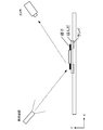
- FIG. 8 A specific example is shown in FIG. As shown in FIG. 8, when an illumination device for emitting light to a component and a camera for imaging are provided at the same angle, the intensity of light reflected by a portion other than the terminal is the intensity of the light reflected by the terminal. It becomes weaker than strength. Therefore, by determining whether the luminance value of the pixel included in the image is equal to or more than the threshold value or less than the threshold value, the region where the terminal exists can be estimated. Also, based on the position on the image, the position, length, angle, etc. of the terminal in space can be determined.
- the luminance values of pixels included in the image range from 0 to 255 in each color (that is, a full color image of 16.77 million colors) and the threshold is 225 or more, all luminance values are 225 to By selecting a pixel in the range of 255, it is possible to extract the region where the terminal exists. Also, the accurate position of the terminal can be calculated based on the extraction result.
- this example is an example in case the light to irradiate is white, irradiated light may be another color, and in that case, you may provide a threshold value for every color.
- the parameter for estimating the area where the terminal is located may be included in the inspection area information or may be stored independently in the component inspection apparatus. Further, the parameter may be defined by values other than RGB as long as it can represent a predetermined range in the color space.
- definition can be made for each terminal, but in the present embodiment, it is assumed that the same parameter is given to a plurality of terminals. Of course, different parameters may be set for each terminal.
- FIG. 9 is an example of terminal information generated by the component inspection device 220.
- the terminal information includes a key (substrate ID, component ID, terminal number) for uniquely identifying the terminal, and information on an area corresponding to the terminal.
- the area where the terminal is located is represented by an XY coordinate system in which the center of the part is the origin and the specific direction of the part is the X axis, as in the inspection area information.
- the “X coordinate (pair part)”, “Y coordinate (pair part)”, “horizontal length”, “vertical length” and “angle (pair part)” shown in the terminal information in FIG. 9 are the inspection areas shown in FIG. 5 respectively. It corresponds to the same item of information, but each item is different in that it is not a value based on a spec but an actual measurement value.
- the terminal information transmitted to the inspection management device 250 is temporarily stored, and is distributed to the appearance inspection device 230 and the X-ray inspection device 240 together with the inspection program used in the post-reflow inspection. Then, when the appearance inspection device 230 and the X-ray inspection device 240 inspect the bonding state of the terminal with respect to the land, the acquired terminal information is referenced to specify the region where the corresponding terminal exists. After the reflow process, since the solder melts, the part sinks in the longitudinal direction (the Z-axis direction in FIG. 8), and the coordinates and angle on the XY plane also change. However, since the relative position of the terminal to the component body does not change, the inspection after the reflow can be performed based on the information acquired before the reflow.
- FIG. 10 is a flowchart of the inspection process performed by the component inspection device 220. The process shown in FIG. 10 is executed at the timing when the printed circuit board to be inspected is loaded. It is assumed that the inspection program is distributed in advance from the inspection management device 250.
- step S11 a camera is used to image a substrate to be inspected.
- the image captured here is an image for measuring the position of the terminal, but may be captured separately if an image for performing a component inspection is further required.
- step S12 the inspection object is extracted by referring to the inspection object information included in the inspection program.
- the inspection object extracted here is either "part" or "terminal”.
- step S13 component inspection is performed on the inspection target to generate an inspection result.
- the inspection may be performed by two-dimensional measurement or three-dimensional measurement.
- step S14 after acquiring the image parameter corresponding to the terminal included in the inspection object from the inspection object information, the region matching the image parameter is extracted from the image acquired in step S11. For example, when the range of the luminance value is 0 to 255 and the image parameter is “luminance value> 225”, an area having a luminance value of 225 or more and 255 or less is extracted. Then, in step S15, a plurality of pieces of terminal information respectively corresponding to the terminals on the substrate are generated based on the extracted area, and transmitted to the inspection management apparatus 250 together with the inspection result generated in step S13.
- FIG. 11 is a flowchart of inspection processing performed by the appearance inspection apparatus 230 and the X-ray inspection apparatus 240. The process shown in FIG. 11 is executed at the timing when the printed circuit board is carried into each inspection device and the inspection is started. It is assumed that the inspection program is distributed in advance from the inspection management device 250.
- step S21 the inspection object is extracted by referring to the inspection object information included in the inspection program.
- the inspection object extracted here is "land”.
- step S22 a terminal corresponding to the land to be inspected is specified with reference to the inspection object information, and terminal information corresponding to the terminal is acquired from the inspection management apparatus 250.
- the position of the terminal joined to the land to be inspected is specified.
- the position of the terminal is estimated using the position information of the terminal included in the inspection object information.
- step S23 inspection (visual inspection or X-ray inspection) is performed on the land to be inspected. When the inspection is completed, the inspection result is generated and transmitted to the inspection management device 250.
- the position of the terminal is detected and stored in advance before entering the reflow process, and the position of the terminal is checked using the information in the post-reflow inspection. Identify In this way, even in the case where the terminals and the solder are integrated by reflow and it becomes difficult to distinguish, the positions of the terminals can be identified accurately. Also, this can improve the accuracy of the post-reflow inspection. That is, since the case where a non-defective product is determined as a non-defective product can be suppressed by an erroneous determination, the inspection cost can be reduced and the productivity can be improved.
- FIG. 12 is a diagram showing another method of defining an area corresponding to a terminal.
- a reference end side (indicated by a thick line) is provided, and the distance A from the end side to the center of the terminal, the width B of the terminal, and the length C of the terminal Defines the position of the terminal.
- the reference side can be identified, as in this example, , Can be defined in three values.
- the inspection management device 250 aggregates all terminal information once and distributes it to the appearance inspection device 230 and the X-ray inspection device 240, but the terminal information is directly transmitted and received between the inspection devices You may Further, although the component inspection apparatus 220 generates terminal information in the description of the embodiment, the terminal information is generated by, for example, the mounter 120 if the location of the terminal of the arranged component can be acquired. It is also good.
Abstract
Provided is a quality management system in a surface mounting line, the system performing: a solder printing step in which a solder is printed onto a printed board by a solder printing device; a mounting step in which an electronic component is disposed on the printed board by a mounter; and a reflow step in which the electronic component is solder-jointed by a reflow furnace. The quality management system comprises: a terminal detection device that, following the mounting step, generates terminal information pertaining to the position of a terminal of the electronic component which has been disposed on the printed board; and a mounting inspection device that, following the reflow step, identifies the position of the terminal belonging to the electronic component on the basis of the terminal information and inspects the state of solder joint between the terminal and the printed board.
Description
本発明は、プリント基板に実装された部品の状態を検査するシステムに関する。
The present invention relates to a system for inspecting the state of a component mounted on a printed circuit board.
プリント基板上に部品を実装する方法のひとつに、表面実装がある。表面実装とは、プリント基板上にはんだペーストを塗布し、実装する部品を載せてから熱を加えてはんだを溶かすことで部品を固定する実装方式である。集積度が高い基板の製造を行えるため、プリント基板上への部品の実装を自動で行う装置では、表面実装が多く用いられている。
One of the methods of mounting components on a printed circuit board is surface mounting. Surface mounting is a mounting method in which a solder paste is applied on a printed circuit board, and after mounting a component to be mounted, heat is applied to melt the solder to fix the component. Since it is possible to manufacture a substrate with a high degree of integration, surface mounting is often used in an apparatus for automatically mounting components on a printed circuit board.
基板への部品の実装を自動化する場合、はんだを冷却した後、正常に基板上に部品が実装されているかを検査する必要がある(以下、リフロー後検査)。特に、部品が有する端子と基板上の電極(ランド)との接続部がはんだによって正常に接合されているか否かを正確に判定することは、製品の品質を担保するうえで重要である。
In the case of automating the mounting of the component on the substrate, it is necessary to check whether the component is properly mounted on the substrate after cooling the solder (hereinafter, post-reflow inspection). In particular, it is important in order to secure product quality that it is accurately determined whether or not the connection between the component's terminal and the electrode (land) on the substrate is properly joined by solder.
リフロー後検査を行うためには、基板上のどの位置にどの部品が載せられているかを正確に検出する必要がある。これに関連する技術として、特許文献1には、部品を基板に積載するマウンタから、部品の接合状態を検査する検査装置に対して、部品の寸法に関する情報を送信し、検査装置が当該情報に基づいて検査すべき箇所を認識する部品実装システムが開示されている。当該システムによると、部品の大きさが個体差によってばらついている場合であっても、検査装置が部品の大きさを正しく認識することができる。
また、特許文献2には、積載された部品を検出し、最も適合する検査ライブラリを選択して検査を実施する方法が記載されている。 In order to perform post-reflow inspection, it is necessary to accurately detect which part is placed on which position on the substrate. As a related technology, in Patent Document 1, the mounter which loads the component on the substrate transmits information on the dimensions of the component to the inspection device which inspects the bonding state of the component, and the inspection device uses the information A component mounting system is disclosed that recognizes a location to be inspected based on the component mounting system. According to the system, the inspection apparatus can correctly recognize the size of the part even if the size of the part varies due to individual differences.
Further, Patent Document 2 describes a method of detecting loaded components, selecting a most suitable inspection library, and performing an inspection.
部品が有する端子と、基板上の電極(ランド)との接合状態を検査する場合、基板上の部品の位置はもちろん、部品が有する端子の先端がどこにあるかを正確に把握する必要がある。端子の先端位置が正しく把握できていないと、はんだフィレットの形成状態や、端子に対するはんだのぬれ上がり状態を正しく判定することができないためである。端子の先端位置は、例えば端子とランドとの接合部分を撮像し、得られた画像を解析することで検出することができる。
When inspecting the bonding state between the terminal of the component and the electrode (land) on the substrate, it is necessary to accurately grasp not only the position of the component on the substrate but also where the tip of the terminal of the component is located. If the tip position of the terminal can not be grasped correctly, the formation state of the solder fillet and the wetting state of the solder to the terminal can not be judged correctly. The tip position of the terminal can be detected, for example, by imaging a junction between the terminal and the land and analyzing the obtained image.
一方、端子がはんだに完全に埋没してしまっているような場合や、端子の上面とはんだが滑らかに繋がっているような場合といったように、端子とはんだとの境界が特定できないケースがある。このようなケースは、特に2ピンミニモールド部品やトランジスタ、一部のSOP(Small Outline Package)部品などで発生しうる。
従来の表面実装ラインでは、このように、端子の先端位置を特定することができない場合、はんだの接合状態を正確に判定することができず、良品を不良品と判定してしまうという問題が発生していた。 On the other hand, there are cases where the boundary between the terminal and the solder can not be identified, such as when the terminal is completely buried in the solder or where the upper surface of the terminal and the solder are smoothly connected. Such a case may occur particularly in 2-pin mini mold parts, transistors, and some SOP (Small Outline Package) parts.
In the conventional surface mounting line, when the tip position of the terminal can not be specified as described above, there is a problem that the bonding state of the solder can not be accurately determined, and a non-defective product is determined as a non-defective product. Was.
特許文献1に記載された部品実装システムでは、実測値に基づいて、プリント基板上の部品の積載位置を特定することができるが、端子の先端位置を検出することはできない。また、特許文献2に記載された方法では、部品を検出して適切な検査ライブラリを選択することはできるが、同様に、端子の先端位置を検出することはできない。
一方、検出した部品の位置を利用して、端子の先端位置を推定するという方法も考えられる。しかし、端子の位置や長さには製造時のばらつきがあるため、必ずしも推定した位置に端子の先端があるとは限らない。 In the component mounting system described in Patent Document 1, although the loading position of the component on the printed circuit board can be specified based on the actual measurement value, the tip position of the terminal can not be detected. Further, the method described in Patent Document 2 can detect parts and select an appropriate inspection library, but can not similarly detect the tip position of the terminal.
On the other hand, there is also conceivable a method of estimating the tip position of the terminal using the position of the detected part. However, since the position and the length of the terminal have variations at the time of manufacture, the tip of the terminal is not necessarily at the estimated position.
本発明は上記の課題を考慮してなされたものであり、表面実装ラインにおいて、はんだ接合状態の検査判定精度を向上させる技術を提供することを目的とする。
The present invention has been made in consideration of the above problems, and an object of the present invention is to provide a technique for improving inspection determination accuracy of a solder joint state in a surface mounting line.
本発明に係る品質管理システムは、はんだ印刷装置によってプリント基板にはんだを印刷するはんだ印刷工程と、マウンタによってプリント基板上に電子部品を配置するマウント工程と、リフロー炉によって電子部品をはんだ接合するリフロー工程とを行う表面実装ラインにおける品質管理システムである。
In the quality control system according to the present invention, a solder printing process for printing solder on a printed circuit board by a solder printing apparatus, a mounting process for placing an electronic component on a printed circuit board by a mounter, and a reflow process for soldering electronic components by a reflow furnace It is a quality control system in the surface mounting line which performs a process.
具体的には、本発明に係る品質管理システムは、前記マウント工程後に、前記プリント基板上に配置された前記電子部品の端子の位置に関する情報である端子情報を生成する端子検出装置と、前記リフロー工程後に、前記端子情報に基づいて、前記電子部品が有する端子の位置を特定し、当該端子とプリント基板とのはんだ接合状態を検査する実装検査装置と、からなることを特徴とする。
Specifically, the quality control system according to the present invention is a terminal detection device that generates terminal information that is information related to the position of the terminal of the electronic component disposed on the printed circuit board after the mounting step; After the process, based on the terminal information, the position of the terminal of the electronic component is specified, and a mounting inspection device for inspecting the solder joint state between the terminal and the printed circuit board is characterized.
端子検出装置は、プリント基板に対する電子部品の配置(マウント)が終了した後で、当該配置された電子部品が有する端子の位置に関する情報である端子情報を生成する手段である。端子情報は、実装検査装置が基板上における端子の位置を特定することができれば、どのような情報であってもよい。例えば、部品に対する端子の相対位置であってもよい。また、端子の幅や長さ、配置角度などに関する情報を含んでいてもよい。
また、実装検査装置は、リフロー工程が終了した後に、電子部品が有する端子と、プリント基板上の電極(ランド)との接合状態を検査する装置である。また、実装検査装置は、端子検出装置が生成した端子情報に基づいて、検査対象の端子がプリント基板上のどこにあるかを特定する。
かかる構成によると、実装検査装置が、検査対象の端子が基板上のどこにあるかを正確に認識することができるため、端子の先端がはんだに埋没しているような場合であっても、端子とランドとの接合状態を正確に判定することができる。 The terminal detection device is means for generating terminal information which is information on the position of the terminal of the electronic component arranged after the arrangement (mounting) of the electronic component on the printed circuit board is completed. The terminal information may be any information as long as the mounting inspection apparatus can specify the position of the terminal on the substrate. For example, it may be the relative position of the terminal to the part. In addition, information on the width and length of the terminal, the arrangement angle, and the like may be included.
In addition, the mounting inspection apparatus is an apparatus for inspecting the bonding state of the terminal of the electronic component and the electrode (land) on the printed board after the reflow process is completed. In addition, the mounting inspection apparatus identifies where on the printed circuit board the terminal to be inspected is based on the terminal information generated by the terminal detection apparatus.
According to such a configuration, the mounting inspection apparatus can accurately recognize where the terminal to be inspected is on the substrate, so even if the tip of the terminal is buried in the solder, the terminal It is possible to accurately determine the bonding state between the and lands.
また、前記端子検出装置は、プリント基板上に配置された電子部品を撮像し、得られた画像に含まれる画素の輝度値に基づいて端子が存在する領域を検出することを特徴としてもよい。
Further, the terminal detection device may be characterized in that an image of an electronic component disposed on a printed circuit board is taken, and a region where the terminal exists is detected based on the luminance value of the pixel included in the obtained image.
部品に対して光を照射した場合、端子によって反射した光と、はんだによって反射した光とでは反射光の特性が異なる。具体的には、端子は光を正反射させ、印刷されたはんだは光を乱反射させる。このため、端子検出装置は、当該特性の違いを光学的に検出することで、端子とはんだとの境界を検出し、端子の位置を特定することができる。
When light is irradiated to a component, the characteristic of reflected light differs between the light reflected by the terminal and the light reflected by the solder. Specifically, the terminals specularly reflect light, and the printed solder diffusely reflects light. For this reason, the terminal detection apparatus can detect the boundary between the terminal and the solder and specify the position of the terminal by optically detecting the difference in the characteristics.
また、前記端子情報は、検査対象の電子部品上に設定された基準位置に対する、端子の相対的な位置関係を表す情報であることを特徴としてもよい。
The terminal information may be information indicating a relative positional relationship of the terminal with respect to a reference position set on the electronic component to be inspected.
基準位置とは、端子の位置を特定するための基準となる位置であり、端子検出装置と実装検査装置によって共有されていれば、どのような位置であってもよい。例えば、部品上に設定された点であってもよい。また、部品の辺縁部などであってもよい。実装検査装置は、基準位置と、基準位置に対する端子の相対的な位置情報を用いて、端子の位置を特定することができる。
The reference position is a position serving as a reference for specifying the position of the terminal, and may be any position as long as it is shared by the terminal detection device and the mounting inspection device. For example, it may be a point set on a part. In addition, it may be an edge portion of a part. The mounting inspection apparatus can specify the position of the terminal using the reference position and the relative position information of the terminal with respect to the reference position.
また、前記端子情報は、前記基準位置に対する、端子の相対位置、端子の幅、端子の長さを表す情報を含むことを特徴としてもよい。
Further, the terminal information may include information indicating a relative position of the terminal, a width of the terminal, and a length of the terminal with respect to the reference position.
基準位置に対する端子の相対的な位置のほか、端子の幅および長さを定義することで、実装検査装置は、検査対象の端子が存在する領域を特定することができる。
By defining the width and length of the terminal in addition to the relative position of the terminal with respect to the reference position, the mounting inspection apparatus can identify the area where the terminal to be inspected is present.
また、前記端子検出装置は、プリント基板上に電子部品を配置するマウンタと、プリント基板上に配置された電子部品の配置状態を検査する部品検査装置のうちの少なくともいずれかであることを特徴としてもよい。
Further, the terminal detection device is at least one of a mounter for arranging an electronic component on a printed circuit board and a component inspection apparatus for inspecting an arrangement state of the electronic component arranged on a printed circuit board. It is also good.
端子情報の生成は、部品を配置した後であれば、部品を配置する装置自体が行ってもよいし、部品の配置状態を検査する装置が行ってもよい。
The generation of the terminal information may be performed by the apparatus for arranging the part itself or after the arrangement of the part may be performed.
また、前記実装検査装置は、プリント基板上の電極と、電子部品が有する端子とのはんだ接合状態を可視光像によって検査する外観検査装置と、プリント基板上の電極と、電子部品が有する端子とのはんだ接合状態を可視光像以外によって検査する内部検査装置のうちの少なくともいずれかであることを特徴としてもよい。
In addition, the mounting inspection apparatus includes an appearance inspection apparatus that inspects a solder joint state between an electrode on a printed circuit board and a terminal of the electronic component using a visible light image, an electrode on the printed circuit board, and a terminal of the electronic component The present invention may be characterized in that it is at least one of internal inspection devices that inspect the solder joint state of the present invention by any means other than visible light images.
このように、実装検査装置は、可視光像によって検査を行う装置であってもよいし、X線などの可視光像以外によって検査を行う装置であってもよい。
As described above, the mounting inspection apparatus may be an apparatus that performs inspection using a visible light image, or may be an apparatus that performs inspection using something other than a visible light image such as an X-ray.
なお、本発明は、上記手段の少なくとも一部を含む品質管理システムとして特定することができる。また、前記品質管理システムの制御方法や、前記品質管理システムを動作させるためのプログラム、当該プログラムが記録された記録媒体として特定することもできる。
上記処理や手段は、技術的な矛盾が生じない限りにおいて、自由に組み合わせて実施することができる。 The present invention can be specified as a quality control system including at least a part of the above means. The control method of the quality control system, the program for operating the quality control system, and the recording medium in which the program is recorded can also be specified.
The above-mentioned processes and means can be freely combined and implemented as long as no technical contradiction arises.
本発明によれば、表面実装ラインにおいて、はんだ接合状態の検査判定精度を向上させることができる。
According to the present invention, in the surface mounting line, the inspection determination accuracy of the solder bonding state can be improved.
(システム構成)
図1は、プリント基板の表面実装ラインにおける生産設備及び品質管理システムの構成例を模式的に示した図である。表面実装(Surface Mount Technology:SMT)とは、プリント基板の表面に電子部品をはんだ付けする技術であり、表面実装ラインは、主として、はんだ印刷~部品のマウント~リフロー(はんだの溶着)の三つの工程から構成される。 (System configuration)
FIG. 1 is a view schematically showing a configuration example of a production facility and a quality control system in a surface mounting line of a printed circuit board. Surface mount technology (SMT) is a technology for soldering electronic components to the surface of a printed circuit board, and surface mount lines mainly consist of three functions: solder printing, mounting of components to reflow (welding of solder). It consists of the process.
図1に示すように、表面実装ラインでは、生産設備として、上流側から順に、はんだ印刷装置110、マウンタ120、リフロー炉130が設けられる。はんだ印刷装置110は、スクリーン印刷によってプリント基板上の電極部(ランドと呼ばれる)にペースト状のはんだを印刷する装置である。マウンタ120は、基板に実装すべき電子部品をピックアップし、該当箇所のはんだペーストの上に部品を載置するための装置であり、チップマウンタとも呼ばれる。リフロー炉130は、はんだペーストを加熱溶融した後、冷却を行い、電子部品を基板上にはんだ接合するための加熱装置である。これらの生産設備110~130は、ネットワーク(LAN)を介して生産設備管理装置140に接続されている。生産設備管理装置140は、生産設備110~130の管理や統括制御を担うシステムであり、各生産設備の動作を定義する実装プログラム(動作手順、製造条件、設定パラメータなどを含む)、各生産設備のログデータなどを記憶、管理、出力する機能などを有している。また、生産設備管理装置140は、作業者又は他の装置から実装プログラムの変更指示を受け付けると、該当する生産設備に設定されている実装プログラムの更新処理を行う機能も有する。
As shown in FIG. 1, in the surface mounting line, a solder printing apparatus 110, a mounter 120, and a reflow furnace 130 are provided in order from the upstream side as a production facility. The solder printing apparatus 110 is an apparatus for printing paste-like solder on electrode parts (called lands) on a printed circuit board by screen printing. The mounter 120 is an apparatus for picking up an electronic component to be mounted on a substrate and placing the component on the solder paste at a corresponding location, and is also called a chip mounter. The reflow furnace 130 is a heating device for performing heating and melting of the solder paste and then cooling to solder-bond the electronic component on the substrate. The production facilities 110 to 130 are connected to the production facility management apparatus 140 via a network (LAN). The production facility management apparatus 140 is a system responsible for management and overall control of the production facilities 110 to 130, and includes an installation program (including operation procedures, manufacturing conditions, setting parameters, etc.) for defining the operation of each production facility, and each production facility. It has functions such as storing, managing and outputting log data of The production facility management apparatus 140 also has a function of updating the mounting program set in the corresponding production facility when receiving an instruction to change the mounting program from the worker or another device.
また、表面実装ラインには、はんだ印刷~部品のマウント~リフローの各工程の出口で基板の状態を検査し、不良あるいは不良のおそれを自動で検出する、品質管理システムが設置されている。品質管理システムは、良品と不良品の自動仕分けの他、検査結果やその分析結果に基づき各生産設備の動作にフィードバックする機能(例えば、実装プログラムの変更など)も有している。
図1に示すように、本実施形態に係る品質管理システムは、はんだ印刷検査装置210、部品検査装置220、外観検査装置230、X線検査装置240の4種類の検査装置と、検査管理装置250、分析装置260、作業端末270などから構成される。 Also, on the surface mounting line, a quality control system is installed that inspects the state of the substrate at the exit of each process of solder printing to mounting of parts to reflow and automatically detects the possibility of defects or defects. The quality control system also has a function (for example, change of a mounting program, etc.) for feeding back to the operation of each production facility based on inspection results and analysis results as well as automatic sorting of non-defective products and defective products.
As shown in FIG. 1, the quality control system according to the present embodiment includes four types of inspection devices, a solderprinting inspection device 210, a component inspection device 220, an appearance inspection device 230, and an X-ray inspection device 240, and an inspection management device 250. , An analyzer 260, a work terminal 270, and the like.
図1に示すように、本実施形態に係る品質管理システムは、はんだ印刷検査装置210、部品検査装置220、外観検査装置230、X線検査装置240の4種類の検査装置と、検査管理装置250、分析装置260、作業端末270などから構成される。 Also, on the surface mounting line, a quality control system is installed that inspects the state of the substrate at the exit of each process of solder printing to mounting of parts to reflow and automatically detects the possibility of defects or defects. The quality control system also has a function (for example, change of a mounting program, etc.) for feeding back to the operation of each production facility based on inspection results and analysis results as well as automatic sorting of non-defective products and defective products.
As shown in FIG. 1, the quality control system according to the present embodiment includes four types of inspection devices, a solder
はんだ印刷検査装置210は、はんだ印刷装置110から搬出された基板に対し、はんだペーストの印刷状態を検査するための装置である。はんだ印刷検査装置210では、基板上に印刷されたはんだペーストを二次元ないし三次元的に計測し、その計測結果から各種の検査項目について正常値(許容範囲)か否かの判定を行う。検査項目としては、例えば、はんだの体積・面積・高さ・位置ずれ・形状などがある。はんだペーストの二次元計測には、イメージセンサ(カメラ)などを用いることができ、三次元計測には、レーザ変位計や、位相シフト法、空間コード化法、光切断法などを利用することができる。
The solder printing inspection apparatus 210 is an apparatus for inspecting the printed state of the solder paste on the substrate carried out of the solder printing apparatus 110. The solder printing inspection apparatus 210 measures the solder paste printed on the substrate two-dimensionally or three-dimensionally, and determines from the measurement results whether or not various inspection items are normal values (acceptable range). The inspection items include, for example, the volume, area, height, positional deviation, shape, etc. of the solder. An image sensor (camera) or the like can be used for two-dimensional measurement of solder paste, and laser displacement meter, phase shift method, space coding method, light cutting method, etc. can be used for three-dimensional measurement. it can.
部品検査装置220は、マウンタ120から搬出された基板に対し、電子部品の配置状態を検査するための装置である。部品検査装置220では、はんだペーストの上に載置された部品(部品本体、電極(リード)など部品の一部でもよい)を二次元ないし三次元的に計測し、その計測結果から各種の検査項目について正常値(許容範囲)か否かの判定を行う。検査項目としては、例えば、部品の位置ずれ、角度(回転)ずれ、欠品(部品が配置されていないこと)、部品違い(異なる部品が配置されていること)、極性違い(部品側と基板側の電極の極性が異なること)、表裏反転(部品が裏向きに配置されていること)、部品高さなどがある。はんだ印刷検査と同様、電子部品の二次元計測には、イメージセンサ(カメラ)などを用いることができ、三次元計測には、レーザ変位計や、位相シフト法、空間コード化法、光切断法などを利用することができる。
The component inspection device 220 is a device for inspecting the arrangement of the electronic components on the substrate carried out of the mounter 120. The part inspection device 220 measures a part (part body, part of the part such as an electrode (lead), etc.) placed on the solder paste two-dimensionally or three-dimensionally, and various inspections are made based on the measurement result. Determine whether the item is a normal value (allowable range). As inspection items, for example, positional deviation of parts, angular (rotational) deviation, missing parts (no parts are arranged), part differences (different parts are arranged), polarity difference (parts side and board The polarity of the electrode on the side is different), the front and back reverse (the part is placed in the reverse direction), the part height, etc. Similar to solder printing inspection, an image sensor (camera) or the like can be used for two-dimensional measurement of electronic components, and for three-dimensional measurement, a laser displacement meter, phase shift method, space coding method, light cutting method Etc. can be used.
外観検査装置230は、リフロー炉130から搬出された基板に対し、はんだ付けの状態を検査するための装置である。外観検査装置230では、リフロー後のはんだ部分を二次元ないし三次元的に計測し、その計測結果から各種の検査項目について正常値(許容範囲)か否かの判定を行う。検査項目としては、部品検査と同じ項目に加え、はんだフィレット形状の良否なども含まれる。はんだの形状計測には、上述したレーザ変位計や、位相シフト法、空間コード化法、光切断法などの他、いわゆるカラーハイライト方式(R、G、Bの照明を異なる入射角ではんだ面に当て、各色の反射光を天頂カメラで撮影することで、はんだの三次元形状を二次元の色相情報として検出する方法)を用いることができる。
The appearance inspection apparatus 230 is an apparatus for inspecting the state of soldering of the substrate carried out of the reflow furnace 130. The appearance inspection apparatus 230 measures the solder portion after reflow in two dimensions or three dimensions, and determines from the measurement results whether or not various inspection items have normal values (acceptable range). The inspection items include the same items as the component inspection as well as the quality of the solder fillet shape. In addition to the above-mentioned laser displacement meter, phase shift method, space coding method, light cutting method and so on for shape measurement of solder, so-called color highlight method (R, G and B illumination surfaces with different incident angles The method of detecting the three-dimensional shape of the solder as two-dimensional hue information) can be used by photographing the reflected light of each color with a zenith camera.
X線検査装置240は、X線像を用いて基板のはんだ付けの状態を検査するための装置(内部検査装置)である。例えば、BGA(Ball Grid Array)、CSP(Chip Size Package)などのパッケージ部品や多層基板の場合には、はんだ接合部が部品や基板の下に隠れているため、外観検査装置230では(つまり外観画像では)はんだの状態を検査することができない。X線検査装置240は、このような外観検査の弱点を補完するための装置である。X線検査装置240の検査項目としては、例えば、部品の位置ずれ、はんだ高さ、はんだ体積、はんだボール径、バックフィレットの長さ、はんだ接合の良否などがある。なお、X線像としては、X線透過画像を用いてもよいし、CT(Computed Tomography)画像を用いることも好ましい。
The X-ray inspection apparatus 240 is an apparatus (internal inspection apparatus) for inspecting the state of soldering of a substrate using an X-ray image. For example, in the case of a package component such as BGA (Ball Grid Array) or CSP (Chip Size Package) or a multilayer substrate, the solder joint is hidden under the component or the substrate, so the appearance inspection device 230 The image can not inspect the condition of the solder). The X-ray inspection apparatus 240 is an apparatus for compensating for the weakness of such visual inspection. The inspection items of the X-ray inspection apparatus 240 include, for example, misalignment of parts, solder height, solder volume, solder ball diameter, back fillet length, and solder joint quality. As the X-ray image, an X-ray transmission image may be used, or a CT (Computed Tomography) image may preferably be used.
これらの検査装置210~240は、ネットワーク(LAN)を介して検査管理装置250に接続されている。検査管理装置250は、検査装置210~240の管理や統括制御を担うシステムであり、各検査装置210~240の動作を定義する検査プログラム(検査手順、検査条件、設定パラメータなど)や、各検査装置210~240で得られた検査結果やログデータなどを記憶、管理、出力する機能などを有している。
分析装置260は、検査管理装置250に集約された各検査装置210~240の検査結果(各工程の検査結果)を分析することで、不良の予測、不良の要因推定などを行う機能や、必要に応じて各生産設備110~130へのフィードバック(実装プログラムの変更など)を行う機能などを有するシステムである。
作業端末270は、生産設備110~130の状態、各検査装置210~240の検査結果、分析装置260の分析結果などの情報を表示する機能、生産設備管理装置140や検査管理装置250に対し実装プログラムや検査プログラムの変更(編集)を行う機能、表面実装ライン全体の動作状況を確認する機能などを有するシステムである。 Theseinspection devices 210 to 240 are connected to the inspection management device 250 via a network (LAN). The inspection management device 250 is a system responsible for management and overall control of the inspection devices 210 to 240, and an inspection program (inspection procedure, inspection conditions, setting parameters, etc.) defining the operation of each inspection device 210 to 240, and each inspection It has a function of storing, managing, and outputting inspection results and log data obtained by the devices 210 to 240.
Theanalysis device 260 analyzes the inspection results (inspection results of each process) of the inspection devices 210 to 240 integrated in the inspection management device 250 to perform failure prediction, failure cause estimation, etc. In accordance with the above, the system has a function of performing feedback (such as changing the mounting program) to each of the production facilities 110 to 130.
Thework terminal 270 has a function of displaying information such as the state of the production facilities 110 to 130, the inspection results of the inspection devices 210 to 240, and the analysis results of the analysis device 260, and is mounted on the production equipment management device 140 and the inspection management device 250. This system has a function to change (edit) a program or inspection program, and a function to check the operation status of the entire surface mounting line.
分析装置260は、検査管理装置250に集約された各検査装置210~240の検査結果(各工程の検査結果)を分析することで、不良の予測、不良の要因推定などを行う機能や、必要に応じて各生産設備110~130へのフィードバック(実装プログラムの変更など)を行う機能などを有するシステムである。
作業端末270は、生産設備110~130の状態、各検査装置210~240の検査結果、分析装置260の分析結果などの情報を表示する機能、生産設備管理装置140や検査管理装置250に対し実装プログラムや検査プログラムの変更(編集)を行う機能、表面実装ライン全体の動作状況を確認する機能などを有するシステムである。 These
The
The
生産設備管理装置140、検査管理装置250、分析装置260はいずれも、CPU(中央演算処理装置)、主記憶装置(メモリ)、補助記憶装置(ハードディスクなど)、入力装置(キーボード、マウス、コントローラ、タッチパネルなど)、表示装置などを具備する汎用的なコンピュータシステムにより構成可能である。これらの装置140、250、260は別々の装置であってもよいが、一つのコンピュータシステムにこれらの装置140、250、260の全ての機能を実装することも可能であるし、生産設備110~130や検査装置210~240のいずれかの装置が具備するコンピュータに、これらの装置140、250、260の機能の全部又は一部を実装することも可能である。また、図1では、生産設備と品質管理システムのネットワークを分けているが、相互にデータ通信が可能であればどのような構成のネットワークを用いてもよい。
The production facility management apparatus 140, the inspection management apparatus 250, and the analysis apparatus 260 are all CPU (central processing unit), main storage (memory), auxiliary storage (such as hard disk), input device (keyboard, mouse, controller, It can be configured by a general-purpose computer system provided with a touch panel and the like, a display device and the like. Although these devices 140, 250, 260 may be separate devices, it is also possible to implement all the functions of these devices 140, 250, 260 in one computer system, and the production facility 110 It is also possible to implement all or a part of the functions of these devices 140, 250, 260 on a computer provided in any of the devices 130 and the inspection devices 210-240. Further, although the production facilities and the network of the quality control system are separated in FIG. 1, any configuration of networks may be used as long as they can mutually communicate data.
(品質管理システムの実施形態)
次に、前述した表面実装ラインにおける、品質管理システムの実施形態について説明する。本実施形態に係る品質管理システムは、部品検査装置220、外観検査装置230、X線検査装置240、および検査管理装置250を含んで構成される。
本実施形態に係る品質管理システムが行う検査の詳細について、データの流れを示した図である図2を参照しながら説明する。 (Embodiment of quality control system)
Next, an embodiment of the quality control system in the surface mounting line described above will be described. The quality control system according to the present embodiment includes acomponent inspection device 220, an appearance inspection device 230, an X-ray inspection device 240, and an inspection management device 250.
The details of the inspection performed by the quality control system according to the present embodiment will be described with reference to FIG. 2 which shows the flow of data.
次に、前述した表面実装ラインにおける、品質管理システムの実施形態について説明する。本実施形態に係る品質管理システムは、部品検査装置220、外観検査装置230、X線検査装置240、および検査管理装置250を含んで構成される。
本実施形態に係る品質管理システムが行う検査の詳細について、データの流れを示した図である図2を参照しながら説明する。 (Embodiment of quality control system)
Next, an embodiment of the quality control system in the surface mounting line described above will be described. The quality control system according to the present embodiment includes a
The details of the inspection performed by the quality control system according to the present embodiment will be described with reference to FIG. 2 which shows the flow of data.
前述したように、部品検査装置220は、基板上に電子部品が正常にマウントされているかを検査する装置である。
また、外観検査装置230およびX線検査装置240は、基板上に配置された電子部品の端子が、基板上のランドに正常にはんだ付けされているか否かを可視光線またはX線によって検査する装置である。すなわち、製品が完成した状態で検査を行う手段である。ここで不良と判定された基板は、不良品として仕分けられ、必要に応じて目視検査などの追加検査に回される。実施形態の説明では、外観検査装置230およびX線検査装置240が行う検査をリフロー後検査と称する。
各検査装置は、検査ライン上に設けられており、搬送される基板に対して検査が実行可能な構成となっている。また、各検査装置は、検査が完了すると、検査結果を検査管理装置250に送信する。 As described above, thecomponent inspection apparatus 220 is an apparatus for inspecting whether the electronic component is properly mounted on the substrate.
Also, thevisual inspection apparatus 230 and the X-ray inspection apparatus 240 are apparatuses that inspect whether the terminals of the electronic component disposed on the substrate are soldered properly to the lands on the substrate using visible light or X-rays. It is. That is, it is a means to inspect in the state where a product was completed. The substrates determined to be defective here are sorted as defectives and are subjected to additional inspection such as visual inspection if necessary. In the description of the embodiment, inspection performed by the appearance inspection device 230 and the X-ray inspection device 240 is referred to as post-reflow inspection.
Each inspection apparatus is provided on an inspection line, and is configured to be capable of performing inspection on a transported substrate. In addition, each inspection device transmits the inspection result to theinspection management device 250 when the inspection is completed.
また、外観検査装置230およびX線検査装置240は、基板上に配置された電子部品の端子が、基板上のランドに正常にはんだ付けされているか否かを可視光線またはX線によって検査する装置である。すなわち、製品が完成した状態で検査を行う手段である。ここで不良と判定された基板は、不良品として仕分けられ、必要に応じて目視検査などの追加検査に回される。実施形態の説明では、外観検査装置230およびX線検査装置240が行う検査をリフロー後検査と称する。
各検査装置は、検査ライン上に設けられており、搬送される基板に対して検査が実行可能な構成となっている。また、各検査装置は、検査が完了すると、検査結果を検査管理装置250に送信する。 As described above, the
Also, the
Each inspection apparatus is provided on an inspection line, and is configured to be capable of performing inspection on a transported substrate. In addition, each inspection device transmits the inspection result to the
ここで問題となるのが、部品とはんだとの配置状態によって、リフロー後検査で誤判定が起こるという問題である。この問題について、ランドと端子がはんだによって接合された部分の断面図である図3を参照しながら説明する。なお、図3中、黒塗りで示した領域が端子であり、ハッチングで示した領域がランドである。
図3に示すように、良品のはんだフィレットは、端子からランドにかけて山の裾野のような広い傾斜面が形成される。これに対し、はんだ不足が起こると、傾斜面の面積が小さくなり、逆にはんだ過多の場合にはフィレットがランド上に盛り上がった形状となる。外観検査装置230およびX線検査装置240は、このような、はんだの形状に基づいて接合状態の判定を行う。 The problem here is the problem that an erroneous determination occurs in the post-reflow inspection depending on the arrangement of the component and the solder. This problem will be described with reference to FIG. 3 which is a cross-sectional view of a portion where lands and terminals are joined by solder. In FIG. 3, the areas shown in black are terminals, and the areas shown in hatching are lands.
As shown in FIG. 3, a good solder fillet has a wide inclined surface such as a foot of a mountain from the terminal to the land. On the other hand, when the solder shortage occurs, the area of the inclined surface becomes smaller, and conversely, in the case of the solder excess, the fillet becomes a raised shape on the land. Theappearance inspection device 230 and the X-ray inspection device 240 determine the bonding state based on such a shape of the solder.
図3に示すように、良品のはんだフィレットは、端子からランドにかけて山の裾野のような広い傾斜面が形成される。これに対し、はんだ不足が起こると、傾斜面の面積が小さくなり、逆にはんだ過多の場合にはフィレットがランド上に盛り上がった形状となる。外観検査装置230およびX線検査装置240は、このような、はんだの形状に基づいて接合状態の判定を行う。 The problem here is the problem that an erroneous determination occurs in the post-reflow inspection depending on the arrangement of the component and the solder. This problem will be described with reference to FIG. 3 which is a cross-sectional view of a portion where lands and terminals are joined by solder. In FIG. 3, the areas shown in black are terminals, and the areas shown in hatching are lands.
As shown in FIG. 3, a good solder fillet has a wide inclined surface such as a foot of a mountain from the terminal to the land. On the other hand, when the solder shortage occurs, the area of the inclined surface becomes smaller, and conversely, in the case of the solder excess, the fillet becomes a raised shape on the land. The
接合状態の判定は、例えば、ランド端から端子端までの長さ、フロントフィレットの長さ、ランドや端子に対するはんだの接触角、はんだのぬれ上がり高さなどに基づいて行うことができる。これらを判定する場合、外観検査装置230およびX線検査装置240は、端子の先端(端子端)が基板上のどこにあるかを認識し、適切な箇所を検査しなければならない。
The determination of the bonding state can be performed based on, for example, the length from the land end to the terminal end, the length of the front fillet, the contact angle of the solder to the land or the terminal, the wetting height of the solder, or the like. In determining these, the visual inspection apparatus 230 and the X-ray inspection apparatus 240 must recognize where the tip of the terminal (terminal end) is on the substrate and inspect an appropriate place.
しかし、端子がはんだに埋没してしまっているケースや、端子とはんだが滑らかに繋がっているケースなど、外観からでは端子の先端位置を判別できない場合がある。図4は、このようなケースを説明する図である。例えば、図4(a)のケースでは、ガルウイングリードがはんだに埋もれてしまい、外部から先端を確認することができない。また、図4(b)のケースでは、端子の上面とはんだが滑らかに繋がっているため、境界がどこにあるかを検出することが難しい。また、図4(c)のケースでは、フラットリードが図4(a)のケースと同様にはんだに埋もれてしまっている。
However, there are cases where the tip position of the terminal can not be determined from the appearance such as the case where the terminal is buried in the solder or the case where the terminal and the solder are connected smoothly. FIG. 4 is a diagram for explaining such a case. For example, in the case of FIG. 4A, the gull wing lead is buried in the solder and the tip can not be confirmed from the outside. Further, in the case of FIG. 4B, since the upper surface of the terminal and the solder are connected smoothly, it is difficult to detect where the boundary is. Further, in the case of FIG. 4 (c), the flat leads are buried in the solder as in the case of FIG. 4 (a).
このようなケースが発生すると、各検査装置において以下のような問題が発生する。
(1)外観検査装置
外観検査装置230は、部品の外観に基づいて検査を行うため、端子の先端が見えない場合、端子の先端位置を推定しなければならない。端子の先端位置は、例えば、検査装置が有している部品の情報に基づいて推定することができる。
しかし、部品には個体差があるため、推定した場所に必ずしも端子端があるとは限らない。また、端子端ではない部分を検査してしまうと、例えずれ幅がミクロン単位であっても、はんだのぬれ角や高さが大きく変化してしまい、結果として、良品と不良品との判定が正しく行えなくなるおそれがある。 When such a case occurs, the following problems occur in each inspection apparatus.
(1) Appearance Inspection Device Theappearance inspection device 230 performs the inspection based on the appearance of the part. Therefore, when the front end of the terminal can not be seen, the front end position of the terminal must be estimated. The tip position of the terminal can be estimated, for example, based on the information of the part that the inspection apparatus has.
However, since there are individual differences in parts, the terminal end is not necessarily at the estimated location. In addition, if the part not at the terminal end is inspected, the wetting angle and height of the solder will greatly change even if the deviation width is in the micron unit, and as a result, it will be judged as good and not good It may not be possible to do it correctly.
(1)外観検査装置
外観検査装置230は、部品の外観に基づいて検査を行うため、端子の先端が見えない場合、端子の先端位置を推定しなければならない。端子の先端位置は、例えば、検査装置が有している部品の情報に基づいて推定することができる。
しかし、部品には個体差があるため、推定した場所に必ずしも端子端があるとは限らない。また、端子端ではない部分を検査してしまうと、例えずれ幅がミクロン単位であっても、はんだのぬれ角や高さが大きく変化してしまい、結果として、良品と不良品との判定が正しく行えなくなるおそれがある。 When such a case occurs, the following problems occur in each inspection apparatus.
(1) Appearance Inspection Device The
However, since there are individual differences in parts, the terminal end is not necessarily at the estimated location. In addition, if the part not at the terminal end is inspected, the wetting angle and height of the solder will greatly change even if the deviation width is in the micron unit, and as a result, it will be judged as good and not good It may not be possible to do it correctly.
(2)X線検査装置
一方、X線検査装置240は、X線を照射して検査を行うため、端子端が埋没しているようなケースであっても、端子とはんだとの透過率の差を検出することで、端子とはんだとの境界を識別することができる。しかし、当該手法を用いた場合、X線を照射する工程に加えて、端子とはんだとを識別する工程が追加で必要となるため、検査時間が余計にかかってしまう。また、端子とはんだとを識別する精度を上げたい場合、境界を鮮明に撮像する必要があるため、撮像時間が増加し、検査時間がより増加してしまう。当該工程を省略することも可能ではあるが、良品と不良品との判定が正しく行えなくなるという、外観検査装置と同様の問題が発生してしまう。 (2) X-ray inspection apparatus On the other hand, since theX-ray inspection apparatus 240 performs inspection by irradiating X-rays, even in the case where the terminal end is buried, the transmittance of the terminal and the solder By detecting the difference, the boundary between the terminal and the solder can be identified. However, in the case of using the method, in addition to the step of irradiating the X-ray, a step of identifying the terminal and the solder is additionally required, and therefore, the inspection time is extra. In addition, in order to increase the accuracy in identifying the terminals and the solder, it is necessary to clearly image the boundary, so the imaging time increases and the inspection time further increases. Although it is possible to omit the process, a problem similar to the appearance inspection apparatus occurs, in which the determination of the non-defective product and the defective product can not be performed correctly.
一方、X線検査装置240は、X線を照射して検査を行うため、端子端が埋没しているようなケースであっても、端子とはんだとの透過率の差を検出することで、端子とはんだとの境界を識別することができる。しかし、当該手法を用いた場合、X線を照射する工程に加えて、端子とはんだとを識別する工程が追加で必要となるため、検査時間が余計にかかってしまう。また、端子とはんだとを識別する精度を上げたい場合、境界を鮮明に撮像する必要があるため、撮像時間が増加し、検査時間がより増加してしまう。当該工程を省略することも可能ではあるが、良品と不良品との判定が正しく行えなくなるという、外観検査装置と同様の問題が発生してしまう。 (2) X-ray inspection apparatus On the other hand, since the
そこで、本実施形態に係る品質管理システムは、マウント工程が終了した後、リフロー工程に進む前に、部品本体に対する端子の位置を確認し、当該端子の位置を一時的に記憶しておき、リフロー後検査において利用する。
具体的には、部品検査装置200が、部品検査を行う際に、端子が存在する領域を抽出し、当該領域の位置を表す情報(以下、端子情報)を生成して、検査結果とともに検査管理装置250に記憶させる。また、リフロー後検査を行う際に、観検査装置230およびX線検査装置240が、検査管理装置250から端子情報を取得し、端子が存在する領域を特定したうえで検査を行う。以下、それぞれの処理について詳しく説明する。 Therefore, the quality control system according to the present embodiment confirms the position of the terminal with respect to the component main body before proceeding to the reflow process after the mounting process is completed, temporarily stores the position of the terminal, and performs the reflow Used in post-testing.
Specifically, when the component inspection apparatus 200 performs component inspection, it extracts an area where a terminal exists, generates information (hereinafter, terminal information) representing the position of the area, and performs inspection management along with the inspection result. It is stored in thedevice 250. In addition, when the post-reflow inspection is performed, the inspection apparatus 230 and the X-ray inspection apparatus 240 acquire terminal information from the inspection management apparatus 250, identify the area where the terminal exists, and perform the inspection. Each processing will be described in detail below.
具体的には、部品検査装置200が、部品検査を行う際に、端子が存在する領域を抽出し、当該領域の位置を表す情報(以下、端子情報)を生成して、検査結果とともに検査管理装置250に記憶させる。また、リフロー後検査を行う際に、観検査装置230およびX線検査装置240が、検査管理装置250から端子情報を取得し、端子が存在する領域を特定したうえで検査を行う。以下、それぞれの処理について詳しく説明する。 Therefore, the quality control system according to the present embodiment confirms the position of the terminal with respect to the component main body before proceeding to the reflow process after the mounting process is completed, temporarily stores the position of the terminal, and performs the reflow Used in post-testing.
Specifically, when the component inspection apparatus 200 performs component inspection, it extracts an area where a terminal exists, generates information (hereinafter, terminal information) representing the position of the area, and performs inspection management along with the inspection result. It is stored in the
最初に、各検査装置が行う検査の概要について説明する。本実施形態に係る品質管理システムでは、検査管理装置250が、前述したように、検査プログラムを各検査装置に配信し、各検査装置が当該検査プログラムを用いて検査を行う。検査プログラムには、検査手順のほか、検査を行う対象についての情報(以下、検査対象情報)が含まれている。
First, an outline of the inspection performed by each inspection device will be described. In the quality management system according to the present embodiment, as described above, the inspection management device 250 distributes the inspection program to each inspection device, and each inspection device performs the inspection using the inspection program. The inspection program includes, in addition to the inspection procedure, information on an object to be inspected (hereinafter referred to as inspection object information).
図5は、検査対象情報のデータ構造を表した例である。検査対象情報には、基板に実装される部品についての情報(部品情報)と、検査領域についての情報(検査領域情報)が含まれている。検査領域とは、検査を行う単位を表したものあり、部品本体であってもよいし、部品が有する端子であってもよい。また、当該端子が接続されるランドであってもよい。検査領域情報には、検査対象の位置や大きさ、角度についての情報と、検査項目や検査基準などが記録されており、各検査装置は、当該情報を参照しながら検査を行う。
FIG. 5 is an example showing the data structure of inspection object information. The inspection target information includes information on parts mounted on the substrate (part information) and information on an inspection area (inspection area information). The inspection area represents a unit to be inspected, and may be a component body or a terminal of a component. Moreover, the land to which the said terminal is connected may be sufficient. The inspection area information includes information on the position, size, and angle of the inspection target, inspection items, inspection criteria, and the like, and each inspection apparatus performs inspection while referring to the information.
図5の例では、部品ごとに、基板を基準とする座標および角度が定義されている。また、検査領域ごとに、部品を基準とする座標および角度が定義されている。なお、検査領域が部品自体である場合、部品を基準とする座標および角度はいずれも0となる。
In the example of FIG. 5, coordinates and angles with respect to the substrate are defined for each part. Further, for each inspection area, coordinates and angles based on the part are defined. When the inspection area is the part itself, the coordinates and the angle based on the part are both zero.
まず、部品検査装置が行う処理について説明する。
部品検査装置220にプリント基板が搬入されると、部品検査装置220は、搬入されたプリント基板の基板IDを取得する。基板IDは、生産設備管理装置140などから取得してもよいし、プリント基板を撮像することで読み取りが可能な場合は、基板から直接読み取ってもよい。そして、搬入されたプリント基板に対応する検査対象情報を検査管理装置250から取得し、部品検査を実行する。 First, processing performed by the component inspection device will be described.
When the printed circuit board is carried into thecomponent inspection device 220, the component inspection device 220 acquires the substrate ID of the carried-in printed circuit board. The substrate ID may be acquired from the production facility management apparatus 140 or the like, or may be read directly from the substrate if the image can be read by imaging the printed circuit board. Then, the inspection object information corresponding to the loaded printed circuit board is acquired from the inspection management apparatus 250, and the component inspection is performed.
部品検査装置220にプリント基板が搬入されると、部品検査装置220は、搬入されたプリント基板の基板IDを取得する。基板IDは、生産設備管理装置140などから取得してもよいし、プリント基板を撮像することで読み取りが可能な場合は、基板から直接読み取ってもよい。そして、搬入されたプリント基板に対応する検査対象情報を検査管理装置250から取得し、部品検査を実行する。 First, processing performed by the component inspection device will be described.
When the printed circuit board is carried into the
部品検査では、検査領域として定義された部品および端子に対して検査を行う。ここで、図5に示した検査対象情報と、検査装置が実際に検査を行う領域との対応関係を、図6および図7を参照しながら説明する。
まず、図6を参照しながら、部品を特定する方法について説明する。図6中、符号601は搬入されたプリント基板を表し、符号602は、当該プリント基板上の、部品が存在する領域を表す。また、図中に示したX軸およびY軸は、部品の位置を表すための軸である。部品の位置は、基板の中心を原点(0,0)としたX-Y座標系で表される。例えば、符号602で表された部品の位置は、部品の中心点の座標(Xp,Yp)と、基板に対する角度(例えばX軸正方向を0度として反時計回りに定義する。本例では0度)で表すことができる。各パラメータは、図5に示した部品情報のうち、それぞれ「X座標(対基板)」「Y座標(対基板)」「角度(対基板)」に対応する。これらの部品情報によって、プリント基板上に配置された部品の位置および姿勢が定義される。 In the part inspection, the parts and terminals defined as the inspection area are inspected. Here, the correspondence between the inspection target information shown in FIG. 5 and the area where the inspection apparatus actually performs the inspection will be described with reference to FIGS. 6 and 7.
First, with reference to FIG. 6, a method of identifying a part will be described. In FIG. 6,reference numeral 601 denotes a loaded printed circuit board, and reference numeral 602 denotes an area on the printed circuit board where a component is present. Also, the X-axis and the Y-axis shown in the figure are axes for representing the position of the part. The position of the part is represented by an XY coordinate system with the center of the substrate as the origin (0, 0). For example, the position of the part represented by reference numeral 602 is defined counterclockwise with the coordinates (Xp, Yp) of the center point of the part and the angle with respect to the substrate (for example, the X-axis positive direction is 0 degree). Can be expressed in degrees). Each parameter corresponds to “X coordinate (to board)”, “Y coordinate (to board)” and “angle (to board)” in the part information shown in FIG. These pieces of component information define the position and attitude of the component placed on the printed circuit board.
まず、図6を参照しながら、部品を特定する方法について説明する。図6中、符号601は搬入されたプリント基板を表し、符号602は、当該プリント基板上の、部品が存在する領域を表す。また、図中に示したX軸およびY軸は、部品の位置を表すための軸である。部品の位置は、基板の中心を原点(0,0)としたX-Y座標系で表される。例えば、符号602で表された部品の位置は、部品の中心点の座標(Xp,Yp)と、基板に対する角度(例えばX軸正方向を0度として反時計回りに定義する。本例では0度)で表すことができる。各パラメータは、図5に示した部品情報のうち、それぞれ「X座標(対基板)」「Y座標(対基板)」「角度(対基板)」に対応する。これらの部品情報によって、プリント基板上に配置された部品の位置および姿勢が定義される。 In the part inspection, the parts and terminals defined as the inspection area are inspected. Here, the correspondence between the inspection target information shown in FIG. 5 and the area where the inspection apparatus actually performs the inspection will be described with reference to FIGS. 6 and 7.
First, with reference to FIG. 6, a method of identifying a part will be described. In FIG. 6,
次に、図7を参照しながら、検査領域を特定する方法について説明する。検査領域の位置は、部品を基準とした位置で表される。図7中、符号701は部品本体を表し、符号702は当該部品が有する端子を表す。また、符号703は当該端子が接続されるランドを表す。また、図中に示したX軸およびY軸は、端子の位置を表すための軸である。端子の位置は、部品の中心を原点(0,0)としたX-Y座標系で表される。例えば、符号702で表された端子は、端子の左下に対応する点704の座標(Xt,Yt)と、端子の横方向の長さWtと、縦方向の長さHt、および部品に対する角度(0度)で表すことができる。各パラメータは、図5に示した検査領域情報のうち、それぞれ「X座標(対部品)」「Y座標(対部品)」「横長さ」「縦長さ」「角度(対部品)」に対応する。
Next, with reference to FIG. 7, a method of specifying an inspection area will be described. The position of the inspection area is represented by the position based on the part. In FIG. 7, reference numeral 701 denotes a component body, and reference numeral 702 denotes a terminal of the component. Further, reference numeral 703 denotes a land to which the terminal is connected. Moreover, the X-axis and Y-axis shown in the figure are axes for representing the position of the terminal. The position of the terminal is represented by an XY coordinate system in which the center of the part is the origin (0, 0). For example, the terminal represented by reference numeral 702 is the coordinates (Xt, Yt) of the point 704 corresponding to the lower left of the terminal, the lateral length Wt of the terminal, the longitudinal length Ht, and the angle to the component ( It can be expressed by 0 degrees). Each parameter corresponds to “X coordinate (pair part)” “Y coordinate (pair part)” “horizontal length” “vertical length” “angle (pair part)” in the inspection area information shown in FIG. .
以上に説明したように、部品情報および検査領域情報によって、検査を行う対象の領域がプリント基板上のどこにあるかが表わされる。
なお、基板に設定された原点は、検査装置間で共有される。すなわち、原点を基準として位置を表わすことで、プリント基板上の領域を一意に特定することができる。
部品検査装置は、このようにして定義された領域に、検査対象の部品や端子が実際に存在するか(すなわち、部品が正しくマウントされているか)を検査し、検査結果を生成して、検査管理装置250に送信する。 As described above, the part information and the inspection area information indicate where the area to be inspected is on the printed circuit board.
In addition, the origin set to the board | substrate is shared between inspection apparatuses. That is, the area on the printed circuit board can be uniquely identified by representing the position with reference to the origin.
The parts inspection apparatus inspects whether the parts and terminals to be inspected actually exist in the area thus defined (that is, whether the parts are correctly mounted), generates an inspection result, and performs inspection. It is transmitted to themanagement device 250.
なお、基板に設定された原点は、検査装置間で共有される。すなわち、原点を基準として位置を表わすことで、プリント基板上の領域を一意に特定することができる。
部品検査装置は、このようにして定義された領域に、検査対象の部品や端子が実際に存在するか(すなわち、部品が正しくマウントされているか)を検査し、検査結果を生成して、検査管理装置250に送信する。 As described above, the part information and the inspection area information indicate where the area to be inspected is on the printed circuit board.
In addition, the origin set to the board | substrate is shared between inspection apparatuses. That is, the area on the printed circuit board can be uniquely identified by representing the position with reference to the origin.
The parts inspection apparatus inspects whether the parts and terminals to be inspected actually exist in the area thus defined (that is, whether the parts are correctly mounted), generates an inspection result, and performs inspection. It is transmitted to the
前述したように、部品や端子の大きさには個体差があるため、同じ部品が実装されていても、プリント基板ごとに、検査対象領域の位置にずれが生じる。もっとも、多少のずれがあっても、部品検査に影響はなく、検査自体を行うことはできる。しかし、リフロー後検査では、当該誤差が検査品質に影響してしまうため、これを防止するため、部品検査装置220は、部品検査の完了後に、端子の正確な位置を表す端子情報を生成する。
As described above, since there are individual differences in the sizes of parts and terminals, even if the same parts are mounted, the position of the inspection target area is shifted for each printed circuit board. However, even if there is a slight deviation, there is no influence on the part inspection, and the inspection itself can be performed. However, in the post-reflow inspection, the error affects the inspection quality, and in order to prevent this, the component inspection device 220 generates terminal information that represents the accurate position of the terminal after the completion of the component inspection.
具体的には、対象の部品をカメラで撮像したうえで、端子部分とはんだ部分とを識別し、端子が存在する領域を抽出する。端子部分とはんだ部分との識別は、例えば、撮像した画像から、特定の色空間に含まれる画素を抽出することで行う。
はんだ接合を行う前の端子は表面が平滑であるため、入射した光が正反射する。これに対して、はんだの表面は平滑ではないため、入射した光が乱反射する。これを利用し、端子が存在する領域と、それ以外の領域を、画素値(輝度値)に基づいて識別することができる。 Specifically, after the target part is imaged by the camera, the terminal portion and the solder portion are identified, and the region where the terminal exists is extracted. The identification between the terminal portion and the solder portion is performed, for example, by extracting pixels included in a specific color space from the captured image.
The terminal before the solder bonding has a smooth surface, so the incident light is specularly reflected. On the other hand, since the surface of the solder is not smooth, incident light is irregularly reflected. Using this, it is possible to identify the area where the terminal is present and the other area based on the pixel value (brightness value).
具体的な例を図8に示す。図8のように、部品に対して光を照射する照明装置と、撮像を行うためのカメラを同一の角度で設けると、端子以外の部分で反射した光の強度は、端子によって反射した光の強度よりも弱くなる。したがって、画像に含まれる画素の輝度値が閾値以上であるか、閾値未満であるかを判定することで、端子が存在する領域を推定することができる。また、画像上の位置に基づいて、空間内における端子の位置、長さ、角度などを求めることができる。
A specific example is shown in FIG. As shown in FIG. 8, when an illumination device for emitting light to a component and a camera for imaging are provided at the same angle, the intensity of light reflected by a portion other than the terminal is the intensity of the light reflected by the terminal. It becomes weaker than strength. Therefore, by determining whether the luminance value of the pixel included in the image is equal to or more than the threshold value or less than the threshold value, the region where the terminal exists can be estimated. Also, based on the position on the image, the position, length, angle, etc. of the terminal in space can be determined.
例えば、画像に含まれる画素の輝度値が、各色で0~255の範囲をとる(すなわち1677万色のフルカラー画像)ものとし、閾値を225以上とすると、RGBそれぞれについて、輝度値が全て225~255の範囲にある画素を選択することで、端子が存在する領域を抽出することができる。また、抽出結果に基づいて端子の正確な位置を算出することができる。なお、本例は照射する光が白色である場合の例であるが、照射光は他の色であってもよいし、その場合、色ごとに閾値を設けてもよい。
なお、端子がある領域を推定するためのパラメータ(例えばRGBごとの輝度の閾値)は、検査領域情報に含ませてもよいし、独立して部品検査装置に記憶させてもよい。また、当該パラメータは、色空間内の所定の範囲を表すことができれば、RGB以外の値によって定義してもよい。
なお、パラメータを検査領域情報に含ませる場合、端子ごとに定義が可能であるが、本実施形態では、複数の端子に対して同一のパラメータが与えられているものとする。もちろん、端子ごとに異なるパラメータを設定してもよい。 For example, assuming that the luminance values of pixels included in the image range from 0 to 255 in each color (that is, a full color image of 16.77 million colors) and the threshold is 225 or more, all luminance values are 225 to By selecting a pixel in the range of 255, it is possible to extract the region where the terminal exists. Also, the accurate position of the terminal can be calculated based on the extraction result. In addition, although this example is an example in case the light to irradiate is white, irradiated light may be another color, and in that case, you may provide a threshold value for every color.
The parameter for estimating the area where the terminal is located (for example, the threshold of the luminance for each RGB) may be included in the inspection area information or may be stored independently in the component inspection apparatus. Further, the parameter may be defined by values other than RGB as long as it can represent a predetermined range in the color space.
When the parameter is included in the inspection area information, definition can be made for each terminal, but in the present embodiment, it is assumed that the same parameter is given to a plurality of terminals. Of course, different parameters may be set for each terminal.
図9は、部品検査装置220が生成する端子情報の例である。端子情報には、端子を一意に識別するためのキー(基板ID,部品ID,端子番号)と、端子に対応する領域についての情報が含まれる。端子がある領域は、検査領域情報と同様に、部品の中心を原点とし、部品の特定方向をX軸としたX-Y座標系にて表される。図9の端子情報に示した「X座標(対部品)」「Y座標(対部品)」「横長さ」「縦長さ」「角度(対部品)」は、それぞれ、図5に示した検査領域情報の同項目に対応するが、各項目はスペックに基づいた値ではなく、実測値であるという点において相違する。
FIG. 9 is an example of terminal information generated by the component inspection device 220. The terminal information includes a key (substrate ID, component ID, terminal number) for uniquely identifying the terminal, and information on an area corresponding to the terminal. The area where the terminal is located is represented by an XY coordinate system in which the center of the part is the origin and the specific direction of the part is the X axis, as in the inspection area information. The “X coordinate (pair part)”, “Y coordinate (pair part)”, “horizontal length”, “vertical length” and “angle (pair part)” shown in the terminal information in FIG. 9 are the inspection areas shown in FIG. 5 respectively. It corresponds to the same item of information, but each item is different in that it is not a value based on a spec but an actual measurement value.
検査管理装置250に送信された端子情報は一時的に記憶され、リフロー後検査にて用いられる検査プログラムとともに、外観検査装置230およびX線検査装置240へ配信される。
そして、外観検査装置230およびX線検査装置240が、ランドに対する端子の接合状態を検査する際に、取得した端子情報を参照して、対応する端子が存在する領域を特定する。なお、リフロー工程を経ると、はんだが溶解するため、部品が縦方向(図8のZ軸方向)に沈み込み、XY平面上での座標および角度も変化する。しかし、部品本体に対する端子の相対位置は変化しないため、リフロー前に取得した情報に基づいて、リフロー後の検査を行うことができる。 The terminal information transmitted to theinspection management device 250 is temporarily stored, and is distributed to the appearance inspection device 230 and the X-ray inspection device 240 together with the inspection program used in the post-reflow inspection.
Then, when theappearance inspection device 230 and the X-ray inspection device 240 inspect the bonding state of the terminal with respect to the land, the acquired terminal information is referenced to specify the region where the corresponding terminal exists. After the reflow process, since the solder melts, the part sinks in the longitudinal direction (the Z-axis direction in FIG. 8), and the coordinates and angle on the XY plane also change. However, since the relative position of the terminal to the component body does not change, the inspection after the reflow can be performed based on the information acquired before the reflow.
そして、外観検査装置230およびX線検査装置240が、ランドに対する端子の接合状態を検査する際に、取得した端子情報を参照して、対応する端子が存在する領域を特定する。なお、リフロー工程を経ると、はんだが溶解するため、部品が縦方向(図8のZ軸方向)に沈み込み、XY平面上での座標および角度も変化する。しかし、部品本体に対する端子の相対位置は変化しないため、リフロー前に取得した情報に基づいて、リフロー後の検査を行うことができる。 The terminal information transmitted to the
Then, when the
(処理フローチャート)
図10は、部品検査装置220が行う検査処理のフローチャートである。図10に示した処理は、検査対象のプリント基板が搬入されたタイミングで実行される。なお、検査プログラムは予め検査管理装置250から配信されているものとする。 (Processing flowchart)
FIG. 10 is a flowchart of the inspection process performed by thecomponent inspection device 220. The process shown in FIG. 10 is executed at the timing when the printed circuit board to be inspected is loaded. It is assumed that the inspection program is distributed in advance from the inspection management device 250.
図10は、部品検査装置220が行う検査処理のフローチャートである。図10に示した処理は、検査対象のプリント基板が搬入されたタイミングで実行される。なお、検査プログラムは予め検査管理装置250から配信されているものとする。 (Processing flowchart)
FIG. 10 is a flowchart of the inspection process performed by the
まず、ステップS11で、カメラを用いて検査対象の基板を撮像する。ここで撮像される画像は、端子の位置を計測するための画像であるが、部品検査を行うための画像が更に必要な場合、別途撮像を行ってもよい。また、複数回撮像を行う場合、それぞれ異なるカメラを用いてもよい。
次に、ステップS12で、検査プログラムに含まれる検査対象情報を参照し、検査対象を抽出する。ここで抽出される検査対象は、「部品」または「端子」のいずれかである。
ステップS13では、検査対象に対する部品検査を実施し、検査結果を生成する。検査は、二次元計測によって行ってもよいし、三次元計測によって行ってもよい。 First, in step S11, a camera is used to image a substrate to be inspected. The image captured here is an image for measuring the position of the terminal, but may be captured separately if an image for performing a component inspection is further required. In addition, when imaging is performed a plurality of times, different cameras may be used.
Next, in step S12, the inspection object is extracted by referring to the inspection object information included in the inspection program. The inspection object extracted here is either "part" or "terminal".
In step S13, component inspection is performed on the inspection target to generate an inspection result. The inspection may be performed by two-dimensional measurement or three-dimensional measurement.
ステップS14では、検査対象に含まれる端子に対応する画像パラメータを検査対象情報から取得したのちに、ステップS11で取得した画像から、当該画像パラメータに一致する領域を抽出する。例えば、輝度値の範囲が0~255であって、画像パラメータが「輝度値>225」であった場合、輝度値が225以上255以下である領域を抽出する。
そして、ステップS15で、抽出した領域に基づいて、基板上の端子にそれぞれ対応する複数の端子情報を生成し、ステップS13で生成した検査結果とともに、検査管理装置250に送信する。 In step S14, after acquiring the image parameter corresponding to the terminal included in the inspection object from the inspection object information, the region matching the image parameter is extracted from the image acquired in step S11. For example, when the range of the luminance value is 0 to 255 and the image parameter is “luminance value> 225”, an area having a luminance value of 225 or more and 255 or less is extracted.
Then, in step S15, a plurality of pieces of terminal information respectively corresponding to the terminals on the substrate are generated based on the extracted area, and transmitted to theinspection management apparatus 250 together with the inspection result generated in step S13.
そして、ステップS15で、抽出した領域に基づいて、基板上の端子にそれぞれ対応する複数の端子情報を生成し、ステップS13で生成した検査結果とともに、検査管理装置250に送信する。 In step S14, after acquiring the image parameter corresponding to the terminal included in the inspection object from the inspection object information, the region matching the image parameter is extracted from the image acquired in step S11. For example, when the range of the luminance value is 0 to 255 and the image parameter is “luminance value> 225”, an area having a luminance value of 225 or more and 255 or less is extracted.
Then, in step S15, a plurality of pieces of terminal information respectively corresponding to the terminals on the substrate are generated based on the extracted area, and transmitted to the
図11は、外観検査装置230およびX線検査装置240が行う検査処理のフローチャートである。図11に示した処理は、各検査装置にプリント基板が搬入され、検査が開始されるタイミングでそれぞれ実行される。なお、検査プログラムは予め検査管理装置250から配信されているものとする。
FIG. 11 is a flowchart of inspection processing performed by the appearance inspection apparatus 230 and the X-ray inspection apparatus 240. The process shown in FIG. 11 is executed at the timing when the printed circuit board is carried into each inspection device and the inspection is started. It is assumed that the inspection program is distributed in advance from the inspection management device 250.
まず、ステップS21で、検査プログラムに含まれる検査対象情報を参照し、検査対象を抽出する。ここで抽出される検査対象は、「ランド」である。
次に、ステップS22で、検査対象情報を参照して、検査対象のランドに対応する端子を特定し、当該端子に対応する端子情報を、検査管理装置250から取得する。本ステップにより、検査対象のランドに接合された端子の位置が特定される。なお、検査対象のランドに対応する端子情報を取得できなかった場合、検査対象情報に含まれる端子の位置情報を用いて端子の位置を推定する。
ステップS23では、検査対象のランドに対する検査(外観検査またはX線検査)を実施する。検査が完了すると、検査結果を生成したのちに、検査管理装置250に送信する。 First, in step S21, the inspection object is extracted by referring to the inspection object information included in the inspection program. The inspection object extracted here is "land".
Next, in step S22, a terminal corresponding to the land to be inspected is specified with reference to the inspection object information, and terminal information corresponding to the terminal is acquired from theinspection management apparatus 250. In this step, the position of the terminal joined to the land to be inspected is specified. When the terminal information corresponding to the land to be inspected can not be acquired, the position of the terminal is estimated using the position information of the terminal included in the inspection object information.
In step S23, inspection (visual inspection or X-ray inspection) is performed on the land to be inspected. When the inspection is completed, the inspection result is generated and transmitted to theinspection management device 250.
次に、ステップS22で、検査対象情報を参照して、検査対象のランドに対応する端子を特定し、当該端子に対応する端子情報を、検査管理装置250から取得する。本ステップにより、検査対象のランドに接合された端子の位置が特定される。なお、検査対象のランドに対応する端子情報を取得できなかった場合、検査対象情報に含まれる端子の位置情報を用いて端子の位置を推定する。
ステップS23では、検査対象のランドに対する検査(外観検査またはX線検査)を実施する。検査が完了すると、検査結果を生成したのちに、検査管理装置250に送信する。 First, in step S21, the inspection object is extracted by referring to the inspection object information included in the inspection program. The inspection object extracted here is "land".
Next, in step S22, a terminal corresponding to the land to be inspected is specified with reference to the inspection object information, and terminal information corresponding to the terminal is acquired from the
In step S23, inspection (visual inspection or X-ray inspection) is performed on the land to be inspected. When the inspection is completed, the inspection result is generated and transmitted to the
以上に説明したように、本実施形態に係る品質管理システムでは、リフロー工程に入る前に、あらかじめ端子の位置を検出して保存しておき、リフロー後検査において、当該情報を用いて端子の位置を特定する。このようにすることで、リフローによって端子とはんだが一体化し、区別がつきにくくなるようなケースであっても、正確に端子の位置を特定することができるようになる。また、これにより、リフロー後検査の精度を向上させることができる。すなわち、誤判定によって、良品を不良品と判定してしまうケースを抑制できるため、検査コストを削減し、生産性を向上させることができる。
As described above, in the quality control system according to the present embodiment, the position of the terminal is detected and stored in advance before entering the reflow process, and the position of the terminal is checked using the information in the post-reflow inspection. Identify In this way, even in the case where the terminals and the solder are integrated by reflow and it becomes difficult to distinguish, the positions of the terminals can be identified accurately. Also, this can improve the accuracy of the post-reflow inspection. That is, since the case where a non-defective product is determined as a non-defective product can be suppressed by an erroneous determination, the inspection cost can be reduced and the productivity can be improved.
(変形例)
なお、実施形態の説明は本発明を説明する上での例示であり、本発明は、発明の趣旨を逸脱しない範囲で適宜変更または組み合わせて実施することができる。 (Modification)
Note that the description of the embodiments is an example for describing the present invention, and the present invention can be implemented by being appropriately changed or combined without departing from the scope of the present invention.
例えば、実施形態の説明では、部品の中心点を原点とする座標系を用いて、端子に対応する領域を表したが、端子に対応する領域は、検査装置が特定可能な方法であれば、どのような方法によって表されてもよい。図12は、端子に対応する領域を定義する他の方法を示した図である。図12の例では、部品の端辺のうち、基準となる端辺(太線で表示)を設け、当該端辺から端子の中心までの距離Aと、端子の幅Bと、端子の長さCによって、端子の位置を定義する。図9の例では5つの値を使用して端子の位置を表わしたが、端子が部品と平行であり、部品の端辺のうち、基準となる端辺が特定できる場合、本例のように、3つの値で定義することができる。
For example, in the description of the embodiment, the area corresponding to the terminal is represented using a coordinate system having the center point of the part as the origin, but if the area corresponding to the terminal can be identified by the inspection apparatus, It may be represented by any method. FIG. 12 is a diagram showing another method of defining an area corresponding to a terminal. In the example of FIG. 12, among the end sides of the component, a reference end side (indicated by a thick line) is provided, and the distance A from the end side to the center of the terminal, the width B of the terminal, and the length C of the terminal Defines the position of the terminal. In the example of FIG. 9, although five values are used to represent the position of the terminal, when the terminal is parallel to the part and among the end sides of the part, the reference side can be identified, as in this example, , Can be defined in three values.
また、実施形態の説明では、検査管理装置250が全ての端子情報を一旦集約して、外観検査装置230およびX線検査装置240に配信したが、端子情報は、検査装置間で直接送受信するようにしてもよい。
また、実施形態の説明では、部品検査装置220が端子情報を生成するようにしたが、配置された部品が有する端子の場所を取得することができれば、端子情報は、例えばマウンタ120によって生成されてもよい。 Further, in the description of the embodiment, theinspection management device 250 aggregates all terminal information once and distributes it to the appearance inspection device 230 and the X-ray inspection device 240, but the terminal information is directly transmitted and received between the inspection devices You may
Further, although thecomponent inspection apparatus 220 generates terminal information in the description of the embodiment, the terminal information is generated by, for example, the mounter 120 if the location of the terminal of the arranged component can be acquired. It is also good.
また、実施形態の説明では、部品検査装置220が端子情報を生成するようにしたが、配置された部品が有する端子の場所を取得することができれば、端子情報は、例えばマウンタ120によって生成されてもよい。 Further, in the description of the embodiment, the
Further, although the
110・・・はんだ印刷装置
120・・・マウンタ
130・・・リフロー炉
140・・・生産設備管理装置
210・・・はんだ印刷検査装置
220・・・部品検査装置
230・・・外観検査装置
240・・・X線検査装置
250・・・検査管理装置
260・・・分析装置
270・・・作業端末 110 ...Solder printing apparatus 120 ... Mounter 130 ... Reflow furnace 140 ... Production facility management apparatus 210 ... Solder printing inspection apparatus 220 ... Component inspection apparatus 230 ... Appearance inspection apparatus 240 · · X-ray inspection device 250 · · · inspection management device 260 · · · analysis device 270 · · · work terminal
120・・・マウンタ
130・・・リフロー炉
140・・・生産設備管理装置
210・・・はんだ印刷検査装置
220・・・部品検査装置
230・・・外観検査装置
240・・・X線検査装置
250・・・検査管理装置
260・・・分析装置
270・・・作業端末 110 ...
Claims (6)
- はんだ印刷装置によってプリント基板にはんだを印刷するはんだ印刷工程と、マウンタによってプリント基板上に電子部品を配置するマウント工程と、リフロー炉によって電子部品をはんだ接合するリフロー工程とを行う表面実装ラインにおける品質管理システムであって、
前記マウント工程後に、前記プリント基板上に配置された前記電子部品の端子の位置に関する情報である端子情報を生成する端子検出装置と、
前記リフロー工程後に、前記端子情報に基づいて、前記電子部品が有する端子の位置を特定し、当該端子とプリント基板とのはんだ接合状態を検査する実装検査装置と、からなる
ことを特徴とする、品質管理システム。 Quality in a surface mounting line that performs a solder printing process that prints solder on a printed circuit board by a solder printing device, a mounting process that places electronic components on a printed circuit board by a mounter, and a reflow process that solders electronic components by a reflow furnace A management system,
A terminal detection device that generates terminal information that is information related to the position of the terminal of the electronic component disposed on the printed circuit board after the mounting step;
After said reflow process, the mounting inspection apparatus which specifies the position of the terminal which the said electronic component has based on the said terminal information, and inspects the solder joint state of the said terminal and a printed circuit board, Quality control system. - 前記端子検出装置は、プリント基板上に配置された電子部品を撮像し、得られた画像に含まれる画素の輝度値に基づいて端子が存在する領域を検出する
ことを特徴とする、請求項1に記載の品質管理システム。 The terminal detection device picks up an electronic component disposed on a printed circuit board, and detects an area where the terminal exists based on the luminance value of the pixel included in the obtained image. Quality control system described in. - 前記端子情報は、検査対象の電子部品上に設定された基準位置に対する、端子の相対的な位置関係を表す情報である
ことを特徴とする、請求項1または2に記載の品質管理システム。 The quality control system according to claim 1, wherein the terminal information is information indicating a relative positional relationship of the terminal with respect to a reference position set on the electronic component to be inspected. - 前記端子情報は、前記基準位置に対する、端子の相対位置、端子の幅、端子の長さを表す情報を含む
ことを特徴とする、請求項3に記載の品質管理システム。 The quality control system according to claim 3, wherein the terminal information includes information indicating a relative position of the terminal, a width of the terminal, and a length of the terminal with respect to the reference position. - 前記端子検出装置は、プリント基板上に電子部品を配置するマウンタと、プリント基板上に配置された電子部品の配置状態を検査する部品検査装置のうちの少なくともいずれかである
ことを特徴とする、請求項1から4のいずれかに記載の品質管理システム。 The terminal detection device is at least one of a mounter for disposing an electronic component on a printed circuit board and a component inspection device for inspecting an arrangement state of the electronic component disposed on the printed circuit board. The quality control system according to any one of claims 1 to 4. - 前記実装検査装置は、プリント基板上の電極と、電子部品が有する端子とのはんだ接合状態を可視光像によって検査する外観検査装置と、プリント基板上の電極と、電子部品が有する端子とのはんだ接合状態を可視光像以外によって検査する内部検査装置のうちの少なくともいずれかである
ことを特徴とする、請求項1から5のいずれかに記載の品質管理システム。 The mounting inspection apparatus is an appearance inspection apparatus for inspecting a solder joint state between an electrode on a printed circuit board and a terminal of an electronic component by a visible light image, a solder on an electrode on a printed circuit board and a terminal of the electronic component The quality control system according to any one of claims 1 to 5, characterized in that it is at least one of internal inspection devices that inspect the bonding state by means other than a visible light image.
Priority Applications (2)
| Application Number | Priority Date | Filing Date | Title |
|---|---|---|---|
| EP15746374.6A EP3104169B1 (en) | 2014-02-06 | 2015-01-27 | Quality management system |
| CN201580004672.2A CN105917217B (en) | 2014-02-06 | 2015-01-27 | Quality control system |
Applications Claiming Priority (2)
| Application Number | Priority Date | Filing Date | Title |
|---|---|---|---|
| JP2014-021287 | 2014-02-06 | ||
| JP2014021287A JP6387620B2 (en) | 2014-02-06 | 2014-02-06 | Quality control system |
Publications (1)
| Publication Number | Publication Date |
|---|---|
| WO2015118997A1 true WO2015118997A1 (en) | 2015-08-13 |
Family
ID=53777804
Family Applications (1)
| Application Number | Title | Priority Date | Filing Date |
|---|---|---|---|
| PCT/JP2015/052211 WO2015118997A1 (en) | 2014-02-06 | 2015-01-27 | Quality management system |
Country Status (4)
| Country | Link |
|---|---|
| EP (1) | EP3104169B1 (en) |
| JP (1) | JP6387620B2 (en) |
| CN (1) | CN105917217B (en) |
| WO (1) | WO2015118997A1 (en) |
Cited By (1)
| Publication number | Priority date | Publication date | Assignee | Title |
|---|---|---|---|---|
| CN110402076A (en) * | 2018-04-25 | 2019-11-01 | 松下知识产权经营株式会社 | Component mounting line, component mounting method and quality control system |
Families Citing this family (2)
| Publication number | Priority date | Publication date | Assignee | Title |
|---|---|---|---|---|
| JP6701571B2 (en) * | 2016-06-28 | 2020-05-27 | 株式会社リコー | Evaluation parts, electronic board, and electronic board production system |
| JP6915981B2 (en) * | 2016-11-17 | 2021-08-11 | ハンファ精密機械株式会社 | Electronic component mounting system and electronic component mounting method |
Citations (6)
| Publication number | Priority date | Publication date | Assignee | Title |
|---|---|---|---|---|
| JPH0372204A (en) * | 1989-08-12 | 1991-03-27 | Matsushita Electric Works Ltd | Checking method of outer appearance of soldering part |
| JPH07321492A (en) * | 1994-05-24 | 1995-12-08 | Matsushita Electric Ind Co Ltd | Quality control method for device mounter |
| JPH09321500A (en) * | 1996-05-28 | 1997-12-12 | Oki Electric Ind Co Ltd | Appearance inspecting method in soldered state |
| JP2006010429A (en) * | 2004-06-24 | 2006-01-12 | Matsushita Electric Ind Co Ltd | Mounted board inspection device |
| JP2007078533A (en) * | 2005-09-14 | 2007-03-29 | Omron Corp | Method of inspecting substrate |
| WO2012096003A1 (en) * | 2011-01-13 | 2012-07-19 | オムロン株式会社 | Solder-attachment inspection method, pcb-inspection system, and solder-attachment inspection device |
Family Cites Families (11)
| Publication number | Priority date | Publication date | Assignee | Title |
|---|---|---|---|---|
| US4988202A (en) * | 1989-06-28 | 1991-01-29 | Westinghouse Electric Corp. | Solder joint inspection system and method |
| JPH0712530A (en) * | 1993-06-24 | 1995-01-17 | Nec Corp | Soldering inspection apparatus |
| JPH10143660A (en) * | 1996-11-11 | 1998-05-29 | Hitachi Ltd | Defective determination processing method and device therefor |
| JP2002108979A (en) * | 2000-09-28 | 2002-04-12 | Sony Corp | Device and method for processing information, quality control system and recording medium |
| DE10152408A1 (en) * | 2000-10-25 | 2002-05-16 | Matsushita Electric Ind Co Ltd | System for automatic mounting of electronic components onto a circuit board uses camera scanning of board |
| CN1354620A (en) * | 2000-11-17 | 2002-06-19 | 由田新技股份有限公司 | Quality maintenance and backtracking system in course of manufacturing printed circuit board |
| JP3873757B2 (en) * | 2002-02-05 | 2007-01-24 | 松下電器産業株式会社 | Electronic component mounting system and electronic component mounting method |
| JP4481192B2 (en) * | 2005-02-24 | 2010-06-16 | ヤマハ発動機株式会社 | Inspection condition management system and component mounting system |
| CN100412853C (en) * | 2005-05-06 | 2008-08-20 | 鸿富锦精密工业(深圳)有限公司 | Producing device monitor system and method |
| JP4681630B2 (en) * | 2008-06-11 | 2011-05-11 | ジヤトコ株式会社 | Quality control system |
| JP5625935B2 (en) * | 2011-01-18 | 2014-11-19 | オムロン株式会社 | Method for determining suitability of judgment reference value, method for specifying proper value thereof, method for changing to proper value, component mounting board inspection system, simulation method and simulation system at production site |
-
2014
- 2014-02-06 JP JP2014021287A patent/JP6387620B2/en active Active
-
2015
- 2015-01-27 EP EP15746374.6A patent/EP3104169B1/en active Active
- 2015-01-27 CN CN201580004672.2A patent/CN105917217B/en active Active
- 2015-01-27 WO PCT/JP2015/052211 patent/WO2015118997A1/en active Application Filing
Patent Citations (6)
| Publication number | Priority date | Publication date | Assignee | Title |
|---|---|---|---|---|
| JPH0372204A (en) * | 1989-08-12 | 1991-03-27 | Matsushita Electric Works Ltd | Checking method of outer appearance of soldering part |
| JPH07321492A (en) * | 1994-05-24 | 1995-12-08 | Matsushita Electric Ind Co Ltd | Quality control method for device mounter |
| JPH09321500A (en) * | 1996-05-28 | 1997-12-12 | Oki Electric Ind Co Ltd | Appearance inspecting method in soldered state |
| JP2006010429A (en) * | 2004-06-24 | 2006-01-12 | Matsushita Electric Ind Co Ltd | Mounted board inspection device |
| JP2007078533A (en) * | 2005-09-14 | 2007-03-29 | Omron Corp | Method of inspecting substrate |
| WO2012096003A1 (en) * | 2011-01-13 | 2012-07-19 | オムロン株式会社 | Solder-attachment inspection method, pcb-inspection system, and solder-attachment inspection device |
Cited By (2)
| Publication number | Priority date | Publication date | Assignee | Title |
|---|---|---|---|---|
| CN110402076A (en) * | 2018-04-25 | 2019-11-01 | 松下知识产权经营株式会社 | Component mounting line, component mounting method and quality control system |
| CN110402076B (en) * | 2018-04-25 | 2022-09-20 | 松下知识产权经营株式会社 | Component mounting line, component mounting method, and quality control system |
Also Published As
| Publication number | Publication date |
|---|---|
| CN105917217A (en) | 2016-08-31 |
| JP2015148507A (en) | 2015-08-20 |
| JP6387620B2 (en) | 2018-09-12 |
| EP3104169A4 (en) | 2017-08-30 |
| EP3104169A1 (en) | 2016-12-14 |
| CN105917217B (en) | 2019-10-18 |
| EP3104169B1 (en) | 2020-09-23 |
Similar Documents
| Publication | Publication Date | Title |
|---|---|---|
| JP6413246B2 (en) | Quality control device and control method for quality control device | |
| JP6144841B2 (en) | Substrate inspection method and substrate inspection system using the same | |
| JP6277754B2 (en) | Quality control system and internal inspection device | |
| JP4103921B2 (en) | Method of setting inspection reference data for fillet inspection, and substrate visual inspection apparatus using this method | |
| US20120327215A1 (en) | High speed optical sensor inspection system | |
| JP5365643B2 (en) | Soldering inspection method, board inspection system, and soldering inspection machine | |
| KR101438157B1 (en) | Board inspection method | |
| JP6451142B2 (en) | Quality control device and control method for quality control device | |
| JP6988499B2 (en) | Inspection management system, inspection management device, inspection management method | |
| JP2006017474A (en) | Printed circuit board tester, printed circuit board assembling and testing line system and program | |
| JP6988500B2 (en) | Inspection management system, inspection management device, inspection management method | |
| JP6922694B2 (en) | Management systems, management devices, management methods, and programs | |
| WO2015118997A1 (en) | Quality management system | |
| JP6295668B2 (en) | Control device for internal inspection device and control method for internal inspection device | |
| JP4228773B2 (en) | Board inspection equipment | |
| JP2008186879A (en) | Substrate inspection method | |
| WO2022157995A1 (en) | Inspection management system, inspection management device, inspection management method, and program | |
| WO2022190543A1 (en) | Information generation device | |
| TW201200868A (en) | Method for inspecting defects of power layer and ground layer of PCB |
Legal Events
| Date | Code | Title | Description |
|---|---|---|---|
| 121 | Ep: the epo has been informed by wipo that ep was designated in this application |
Ref document number: 15746374 Country of ref document: EP Kind code of ref document: A1 |
|
| REEP | Request for entry into the european phase |
Ref document number: 2015746374 Country of ref document: EP |
|
| WWE | Wipo information: entry into national phase |
Ref document number: 2015746374 Country of ref document: EP |
|
| NENP | Non-entry into the national phase |
Ref country code: DE |