WO2015111490A1 - Non-reciprocal circuit element - Google Patents
Non-reciprocal circuit element Download PDFInfo
- Publication number
- WO2015111490A1 WO2015111490A1 PCT/JP2015/050887 JP2015050887W WO2015111490A1 WO 2015111490 A1 WO2015111490 A1 WO 2015111490A1 JP 2015050887 W JP2015050887 W JP 2015050887W WO 2015111490 A1 WO2015111490 A1 WO 2015111490A1
- Authority
- WO
- WIPO (PCT)
- Prior art keywords
- input
- center electrode
- output port
- series
- resistance element
- Prior art date
Links
Images


Classifications
-
- H—ELECTRICITY
- H01—ELECTRIC ELEMENTS
- H01P—WAVEGUIDES; RESONATORS, LINES, OR OTHER DEVICES OF THE WAVEGUIDE TYPE
- H01P1/00—Auxiliary devices
- H01P1/32—Non-reciprocal transmission devices
- H01P1/36—Isolators
-
- H—ELECTRICITY
- H01—ELECTRIC ELEMENTS
- H01P—WAVEGUIDES; RESONATORS, LINES, OR OTHER DEVICES OF THE WAVEGUIDE TYPE
- H01P1/00—Auxiliary devices
- H01P1/32—Non-reciprocal transmission devices
- H01P1/38—Circulators
- H01P1/383—Junction circulators, e.g. Y-circulators
-
- H—ELECTRICITY
- H01—ELECTRIC ELEMENTS
- H01P—WAVEGUIDES; RESONATORS, LINES, OR OTHER DEVICES OF THE WAVEGUIDE TYPE
- H01P1/00—Auxiliary devices
- H01P1/32—Non-reciprocal transmission devices
- H01P1/38—Circulators
- H01P1/383—Junction circulators, e.g. Y-circulators
- H01P1/387—Strip line circulators
-
- H—ELECTRICITY
- H03—ELECTRONIC CIRCUITRY
- H03H—IMPEDANCE NETWORKS, e.g. RESONANT CIRCUITS; RESONATORS
- H03H7/00—Multiple-port networks comprising only passive electrical elements as network components
- H03H7/01—Frequency selective two-port networks
- H03H7/0115—Frequency selective two-port networks comprising only inductors and capacitors
-
- H—ELECTRICITY
- H03—ELECTRONIC CIRCUITRY
- H03H—IMPEDANCE NETWORKS, e.g. RESONANT CIRCUITS; RESONATORS
- H03H7/00—Multiple-port networks comprising only passive electrical elements as network components
- H03H7/18—Networks for phase shifting
-
- H—ELECTRICITY
- H03—ELECTRONIC CIRCUITRY
- H03H—IMPEDANCE NETWORKS, e.g. RESONANT CIRCUITS; RESONATORS
- H03H7/00—Multiple-port networks comprising only passive electrical elements as network components
- H03H7/52—One-way transmission networks, i.e. unilines
-
- H—ELECTRICITY
- H05—ELECTRIC TECHNIQUES NOT OTHERWISE PROVIDED FOR
- H05K—PRINTED CIRCUITS; CASINGS OR CONSTRUCTIONAL DETAILS OF ELECTRIC APPARATUS; MANUFACTURE OF ASSEMBLAGES OF ELECTRICAL COMPONENTS
- H05K1/00—Printed circuits
- H05K1/18—Printed circuits structurally associated with non-printed electric components
- H05K1/182—Printed circuits structurally associated with non-printed electric components associated with components mounted in the printed circuit board, e.g. insert mounted components [IMC]
Definitions
- the present invention relates to non-reciprocal circuit elements, and more particularly to non-reciprocal circuit elements such as isolators and circulators used in the microwave band.
- nonreciprocal circuit elements such as isolators and circulators have a characteristic of transmitting a signal only in a predetermined specific direction and not transmitting in a reverse direction. Utilizing this characteristic, for example, an isolator is used in a transmission circuit unit of a mobile communication device such as a mobile phone.
- Patent Document 1 discloses that two center electrodes 21 and 22 (inductance elements L1 and L2) formed on a ferrite 10 and capacitors C1 and C2 are 2 as shown in FIG. A pair of LC parallel resonance circuits is configured, and a resistor element R is connected in series between one end of each of the center electrodes 21 and 22 is described.
- Patent Document 2 it is described that the isolation characteristic is broadened by connecting an LC series resonance circuit to a resistance element.
- the technique described in Patent Document 2 attempts to widen the isolation characteristic by matching the resistance element to a wide band according to the resonance characteristic of the LC series resonance circuit.
- JP 2001-237613 A Japanese Patent No. 4155342
- An object of the present invention is to provide a non-reciprocal circuit device capable of obtaining good isolation characteristics over a wide band.
- the nonreciprocal circuit device is A magnetic material to which a DC magnetic field is applied by a permanent magnet; A plurality of central electrodes arranged to intersect with each other in a magnetically insulated state; With Of the plurality of center electrodes, one end of the first center electrode is connected to the first input / output port, and one end of the second center electrode is connected to the second input / output port.
- a resistance element is connected in series between the first input / output port and the second input / output port, and a phase shift circuit is connected in series to the resistance element; It is characterized by.
- the non-reciprocal circuit device is A magnetic material to which a DC magnetic field is applied by a permanent magnet; A first center electrode, a second center electrode, and a third center electrode, which are arranged in an insulating state and intersecting the magnetic body; With The first center electrode has one end connected to the first input / output port and the other end connected to the ground.
- the third center electrode has one end connected to the third input / output port, the other end connected to the ground, Capacitance elements are respectively connected in parallel to the first center electrode, the second center electrode, and the third center electrode to form a first LC parallel resonance circuit, a second LC parallel resonance circuit, and a third LC parallel resonance circuit, A resistance element is connected in series between the first input / output port and the second input / output port, and a phase shift circuit is connected in series to the resistance element; It is characterized by.
- the non-reciprocal circuit device is A magnetic material to which a DC magnetic field is applied by a permanent magnet; A first center electrode and a second center electrode, which are arranged in an insulating state and intersecting the magnetic body; With The first center electrode has one end connected to the first input / output port and the other end connected to the ground.
- Capacitance elements are respectively connected in parallel to the first center electrode and the second center electrode to form a first LC parallel resonance circuit and a second LC parallel resonance circuit, A resistance element is connected in series between the first input / output port and the second input / output port, and a phase shift circuit is connected in series to the resistance element; It is characterized by.
- the nonreciprocal circuit element when a high frequency signal is input in the opposite direction, a phase difference in potential occurs between the first input / output port and the second input / output port, and a current flows through the resistance element to increase the high frequency signal. Attenuated. Since the phase shift circuit is connected in series with the resistance element, this phase difference becomes large over a wide band, and the isolation characteristic is improved over the wide band.
- FIG. 3 is an exploded perspective view showing the ferrite / magnet assembly shown in FIG. 2. It is a graph which shows the phase characteristic of the said nonreciprocal circuit element. It is a graph which shows the isolation characteristic of the said nonreciprocal circuit element. It is a graph which shows the insertion loss characteristic of the said nonreciprocal circuit element. It is the equivalent circuit schematic of the nonreciprocal circuit device which is 2nd Example. It is the equivalent circuit schematic of the nonreciprocal circuit device which is 3rd Example. It is the equivalent circuit schematic of the nonreciprocal circuit device which is 4th Example. It is the equivalent circuit schematic of the nonreciprocal circuit device which is 5th Example. It is an equivalent circuit diagram of the conventional nonreciprocal circuit device. It is a graph which shows the phase characteristic of the nonreciprocal circuit device shown in FIG.
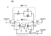
- the nonreciprocal circuit device is constituted by an equivalent circuit shown in FIG. That is, a pair of permanent magnets 31 (see FIGS. 2 and 3), a magnetic body 10 to which a DC magnetic field is applied by the permanent magnets 31 (hereinafter referred to as ferrite), and the ferrite 10 are arranged so as to cross each other in an insulated state.
- the first center electrode 21 and the second center electrode 22 are provided.
- the first center electrode 21 has one end connected to the first input / output port P1 and the other end connected to the ground.
- the second center electrode 22 has one end connected to the second input / output port P2 and the other end connected to the ground.
- Capacitance elements C1 and C2 are connected in parallel to the first center electrode 21 and the second center electrode 22, respectively, to form a first LC parallel resonance circuit and a second LC parallel resonance circuit.
- a resistance element R is connected in series between the first input / output port P1 and the second input / output port P2, and a phase shift circuit (an LC parallel resonance circuit including an inductance element L5 and a capacitance element C5) is provided.
- the resistor element R is connected in series.
- an input impedance matching capacitive element Cs1 is connected between the first input / output port P1 and the input terminal IN.
- a capacitive element Cs2 for output impedance matching is connected between the second input / output port P2 and the output terminal OUT.
- the two-port isolator 1 having the above circuit configuration, when a high-frequency signal is input from the input terminal IN to the port P1 (forward direction), the ports P1 and P2 are in phase and no current flows through the resistance element R. Therefore, it is transmitted to the output terminal OUT with a small insertion loss. Since a high frequency signal does not flow through the LC parallel resonance circuit composed of the inductance element L5 and the capacitive element C5, the insertion loss does not increase.
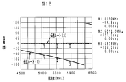
- FIG. 4 shows the phase difference characteristics in the reverse direction in the first embodiment.
- FIG. 12 shows the phase difference characteristics in the reverse direction in the conventional example shown in FIG.
- the first embodiment shown in FIG. 4 produces a larger phase difference than the conventional example shown in FIG.
- the phase differences at each frequency are shown in Tables 1A and 1B below.
- the phase differences at each frequency in the forward direction are shown in Tables 1C and 1D below.
- the isolation characteristic of the conventional example shown in FIG. 11 is as shown by a curve B in FIG.
- the frequency band having an isolation characteristic of 15 dB or less is wider than that of the conventional example, and the isolation characteristic is improved over a wide band.
- the attenuation amount of the isolation characteristic at each frequency is shown in Table 1E below.
- the specific insertion loss characteristic is as shown by the curve A in FIG.
- the insertion loss characteristic of the conventional example shown in FIG. 11 is as shown by a curve B in FIG.
- the insertion loss near 5150 MHz is improved in the first embodiment. This is because the resonant frequency of the LC parallel resonant circuit composed of the inductance element L5 and the capacitive element C5 is set near 5150 MHz, so that the impedance on the transmission route (2) side to which the resistance element R is connected is infinite at that frequency. This is because the high frequency signal hardly flows to the resistance element R.
- the isolation characteristic is broadened by connecting an LC series resonance circuit to the resistance element.
- the broadband of the isolation characteristic is achieved by matching the resistance element in a wide band by the impedance characteristic of the LC series resonance circuit.
- the LC parallel resonant circuit composed of the elements L5 and C5 is connected in series to the resistance element R, so that the transmission routes (1) and (2) The phase difference of the high frequency signal is increased to improve the isolation characteristics.
- the lumped constant type two-port isolator 1 includes a ferrite / magnet assembly 9 in which permanent magnets 31 are bonded to the front and back surfaces of the ferrite 10 via adhesives 32, respectively.
- the assembly 9 is mounted on the multilayer substrate 6 so that the main surface of the ferrite 10 is in the vertical direction.
- a yoke 8 is disposed immediately above the assembly 9.
- the first center electrode 21 is wound around the front and back surfaces of the ferrite 10 for one turn, the one end electrode 21a is the port P1, and the other end electrode 21b is the ground port.
- the second center electrode 22 is wound four turns on the front and back surfaces of the ferrite 10 so as to intersect with the first center electrode 21 at a predetermined angle while maintaining an insulating state. The number of windings is arbitrary.
- One end electrode 22a of the second center electrode 22 is a port P2, and the other end is common (ground port) with the electrode 21b.
- FIG. 3 the illustration of the electrode on the back side of the ferrite 10 is omitted to avoid complication.
- the circuit elements (capacitance elements C1, C2, C5, Cs1, Cs2, inductance element L5) are built in the multilayer substrate 6. By incorporating at least one of these circuit elements in the multilayer substrate 6, the isolator 1 can be reduced in size.
- phase difference between the high-frequency signal (reverse direction) that is input from the output terminal OUT and flows through the transmission route (1) and the high-frequency signal that flows through the transmission route (2) is closer to 180 degrees, the better effect is obtained. For this reason, even if it is not the LC parallel resonance circuit, the phase difference between the high-frequency signal (reverse direction) flowing through the transmission route (1) and the high-frequency signal flowing through the transmission route (2) is brought close to 180 degrees in a predetermined frequency band. It is only necessary to provide a phase shift circuit having a function. As an example of such a phase shift circuit, for example, a stripline type transmission line can be used.
- the nonreciprocal circuit element (two-port isolator 2) according to the second embodiment has a reactance element X connected in parallel to the resistance element R, as shown in FIG.
- the configuration is the same as that of the isolator 1 according to one embodiment.
- the operational effect of the second embodiment is basically the same as that of the first embodiment.
- This type of capacitive element or inductance element may be mounted on a multilayer substrate as a chip type, or may be formed and incorporated as an internal electrode on the multilayer substrate.
- the capacitance value and the inductance value can be adjusted by cutting the internal electrode pattern with a laser or a leuter.
- the nonreciprocal circuit device (2-port isolator 3) according to the third embodiment is one in which a capacitive element Cj is further connected in series between the first port P1 and the output terminal OUT.
- Other configurations are the same as those of the isolator 1 according to the first embodiment.
- the operational effects of the third embodiment are basically the same as those of the first embodiment.
- the capacitive element Cj is for impedance matching between the ports P1 and P2, and by changing the capacitance value of the capacitive element Cj, the attenuation of the isolation characteristic and the insertion loss characteristic can be finely adjusted. Therefore, by providing the capacitive element Cj, desired characteristics can be easily obtained.
- the nonreciprocal circuit device (four-port circulator 4) of the fourth embodiment has the other end of the first center electrode 21 and the other end of the second center electrode 22 connected to the third input / output port P3.
- the port P3 is connected to the input / output terminal T3 via the impedance matching capacitive element Cs3.
- an input / output unit at one end (input / output port P1) of the first center electrode 21 is a terminal T1
- an input / output unit at one end (input / output port P2) of the second center electrode 22 is a terminal T2.
- Other configurations are basically the same as those of the isolator 1 according to the first embodiment.
- the high frequency signal input to the terminal T1 is transmitted to the terminal T2.
- the high-frequency signal input to the terminal T2 is mainly transmitted to the terminal T3 based on the resonance frequencies of the elements L2 and C2, and the signal component transmitted from the terminal T2 to the terminal T1 is attenuated by the resistance element R. Further, as described in the first embodiment, the phase difference between the LC parallel resonant circuit transmission route 1 and the transmission route 2 is adjusted to 180 degrees by the elements L5 and C5, and the isolation characteristics are improved.
- the high-frequency signal input to the terminal T3 is transmitted to the terminal T1 based on the resonance frequency of the elements L1 and C1, and is not transmitted to the terminal T2.
- the nonreciprocal circuit device (three-port circulator 5) according to the fifth embodiment has a third center electrode 23 as a ferrite 10 in addition to the first center electrode 21 and the second center electrode 22.
- the center electrodes 21 and 22 are arranged so as to intersect with each other in an insulated state.
- One end of the third center electrode 23 corresponds to the third input / output port P3, and the port P3 is connected to the terminal T3 via the impedance matching capacitive element Cs3.
- the other end of the third center electrode 23 is connected to the ground.
- the capacitive element C3 is connected in parallel to the third center electrode 23 to form a third parallel resonant circuit.
- an input / output unit at one end (input / output port P1) of the first center electrode 21 is a terminal T1
- an input / output unit at one end (input / output port P2) of the second center electrode 22 is a terminal T2.
- Other configurations are basically the same as those of the isolator 1 according to the first embodiment.
- the high-frequency signal input to the terminal T1 is transmitted to the terminal T2.
- the high-frequency signal input to the terminal T2 is transmitted to the terminal T3 based on the resonance frequencies of the elements L2 and C2 and the resonance frequencies of the elements L3 and C3, and the signal component leaking to the terminal T1 is attenuated by the resistance element R.
- the phase difference between the LC parallel resonant circuit transmission route 1 and the transmission route 2 is adjusted to 180 degrees by the elements L5 and C5, and the isolation characteristic between the terminal T1 and the terminal T2 is adjusted. Will be good.
- the high-frequency signal input to the terminal T3 is transmitted to the terminal T1 based on the resonance frequencies of the elements L1 and C1 and the resonance frequencies of the elements L3 and C3, and transmitted to the terminal T2 due to the irreversibility of the ferrite. Absent.
- a circuit including a resistor R and elements L5 and C5 installed between the input / output ports P1 and P2 is provided between the input / output ports P2 and P3 or between the input / output ports P3 and P1. Also good.
- the element value of element L5, C5 can be adjusted appropriately between each port, and the isolation characteristic between each port can be made favorable.
- the non-reciprocal circuit device according to the present invention is not limited to the above-described embodiments, and can be variously modified within the scope of the gist thereof.
- the configuration of the ferrite / magnet assembly 9, in particular, the shapes of the first and second center electrodes 21, 22 are arbitrary.
- the present invention is useful for non-reciprocal circuit devices, and is particularly excellent in that good isolation characteristics can be obtained over a wide band.
Abstract
In order to obtain a favorable isolation characteristic over a wide band in a non-reciprocal circuit element, a non-reciprocal circuit element is provided with a magnetic body (10) to which a direct-current magnetic field is applied by a permanent magnet, and a plurality of center electrodes which are disposed on the magnetic body (10) to cross each other in isolated states. Among the plurality of center electrodes, a first center electrode (21) has one end connected to a first input/output port (P1), and a second center electrode (22) has one end connected to a second input/output port (P2). A resistance element (R) is connected in series between the ports (P1, P2), and a phase-shift circuit (a parallel resonance circuit composed of an inductance element (L5) and a capacitive element (C5)) is connected in series with the resistance element (R).
Description
本発明は、非可逆回路素子、特に、マイクロ波帯で使用されるアイソレータやサーキュレータなどの非可逆回路素子に関する。
The present invention relates to non-reciprocal circuit elements, and more particularly to non-reciprocal circuit elements such as isolators and circulators used in the microwave band.
従来より、アイソレータやサーキュレータなどの非可逆回路素子は、予め定められた特定方向にのみ信号を伝送し、逆方向には伝送しない特性を有している。この特性を利用して、例えば、アイソレータは、携帯電話などの移動体通信機器の送信回路部に使用されている。
Conventionally, nonreciprocal circuit elements such as isolators and circulators have a characteristic of transmitting a signal only in a predetermined specific direction and not transmitting in a reverse direction. Utilizing this characteristic, for example, an isolator is used in a transmission circuit unit of a mobile communication device such as a mobile phone.
この種の非可逆回路素子として、特許文献1には、図11に示すように、フェライト10に形成した2本の中心電極21,22(インダクタンス素子L1,L2)とコンデンサC1,C2とで2組のLC並列共振回路を構成し、中心電極21,22のそれぞれの一端間に抵抗素子Rを直列に接続したものが記載されている。
As this type of non-reciprocal circuit element, Patent Document 1 discloses that two center electrodes 21 and 22 (inductance elements L1 and L2) formed on a ferrite 10 and capacitors C1 and C2 are 2 as shown in FIG. A pair of LC parallel resonance circuits is configured, and a resistor element R is connected in series between one end of each of the center electrodes 21 and 22 is described.
特許文献1に記載の非可逆回路素子においては、入力端子INに高周波信号が入力されると(順方向)、ポートP1,P2が同位相となり、抵抗素子Rに電流が流れないので挿入損失が小さくなる。一方、出力端子OUTに高周波電流が入力されると(逆方向)、ポートP1,P2に電位の位相差が発生し、抵抗素子Rに電流が流れて高周波電流が大きく減衰される(アイソレーション特性が得られる)。
In the non-reciprocal circuit element described in Patent Document 1, when a high frequency signal is input to the input terminal IN (forward direction), the ports P1 and P2 are in phase, and no current flows through the resistance element R, so insertion loss is reduced. Get smaller. On the other hand, when a high-frequency current is input to the output terminal OUT (reverse direction), a phase difference in potential occurs between the ports P1 and P2, and a current flows through the resistance element R, so that the high-frequency current is greatly attenuated (isolation characteristics). Is obtained).
しかしながら、ポートP1,P2の電位の位相差が大きくなる高周波信号の周波数領域が限定されることから、広帯域にわたって好ましいアイソレーション特性を得ることが困難であった。
However, since the frequency region of the high-frequency signal in which the phase difference between the potentials of the ports P1 and P2 becomes large is limited, it is difficult to obtain preferable isolation characteristics over a wide band.
また、特許文献2には、抵抗素子にLC直列共振回路を接続することにより、アイソレーション特性を広帯域化することが記載されている。特許文献2に記載の技術は、LC直列共振回路の共振特性により抵抗素子を広帯域に整合させることにより、アイソレーション特性の広帯域化を図っている。
In Patent Document 2, it is described that the isolation characteristic is broadened by connecting an LC series resonance circuit to a resistance element. The technique described in Patent Document 2 attempts to widen the isolation characteristic by matching the resistance element to a wide band according to the resonance characteristic of the LC series resonance circuit.
本発明の目的は、広帯域にわたって良好なアイソレーション特性を得ることのできる非可逆回路素子を提供することにある。
An object of the present invention is to provide a non-reciprocal circuit device capable of obtaining good isolation characteristics over a wide band.
本発明の第1の形態である非可逆回路素子は、
永久磁石により直流磁界が印加される磁性体と、
前記磁性体に互いに絶縁状態で交差して配置された複数の中心電極と、
を備え、
前記複数の中心電極のうち、第1中心電極はその一端が第1入出力ポートに接続され、第2中心電極はその一端が第2入出力ポートに接続され、
第1入出力ポートと第2入出力ポートとの間に抵抗素子が直列に接続されるとともに、移相回路が前記抵抗素子に直列に接続されていること、
を特徴とする。 The nonreciprocal circuit device according to the first aspect of the present invention is
A magnetic material to which a DC magnetic field is applied by a permanent magnet;
A plurality of central electrodes arranged to intersect with each other in a magnetically insulated state;
With
Of the plurality of center electrodes, one end of the first center electrode is connected to the first input / output port, and one end of the second center electrode is connected to the second input / output port.
A resistance element is connected in series between the first input / output port and the second input / output port, and a phase shift circuit is connected in series to the resistance element;
It is characterized by.
本発明の第2の形態である非可逆回路素子は、
永久磁石により直流磁界が印加される磁性体と、
前記磁性体に互いに絶縁状態で交差して配置された第1中心電極、第2中心電極及び第3中心電極と、
を備え、
第1中心電極はその一端が第1入出力ポートに接続され、他端がグランドに接続され、
第2中心電極はその一端が第2入出力ポートに接続され、他端がグランドに接続され、
第3中心電極はその一端が第3入出力ポートに接続され、他端がグランドに接続され、
第1中心電極、第2中心電極及び第3中心電極にそれぞれ容量素子が並列に接続されて第1LC並列共振回路、第2LC並列共振回路及び第3LC並列共振回路が形成されており、
第1入出力ポートと第2入出力ポートとの間に抵抗素子が直列に接続されるとともに、移相回路が前記抵抗素子に直列に接続されていること、
を特徴とする。 The non-reciprocal circuit device according to the second aspect of the present invention is
A magnetic material to which a DC magnetic field is applied by a permanent magnet;
A first center electrode, a second center electrode, and a third center electrode, which are arranged in an insulating state and intersecting the magnetic body;
With
The first center electrode has one end connected to the first input / output port and the other end connected to the ground.
One end of the second center electrode is connected to the second input / output port, the other end is connected to the ground,
The third center electrode has one end connected to the third input / output port, the other end connected to the ground,
Capacitance elements are respectively connected in parallel to the first center electrode, the second center electrode, and the third center electrode to form a first LC parallel resonance circuit, a second LC parallel resonance circuit, and a third LC parallel resonance circuit,
A resistance element is connected in series between the first input / output port and the second input / output port, and a phase shift circuit is connected in series to the resistance element;
It is characterized by.
本発明の第3の形態である非可逆回路素子は、
永久磁石により直流磁界が印加される磁性体と、
前記磁性体に互いに絶縁状態で交差して配置された第1中心電極及び第2中心電極と、
を備え、
第1中心電極はその一端が第1入出力ポートに接続され、他端がグランドに接続され、
第2中心電極はその一端が第2入出力ポートに接続され、他端がグランドに接続され、
第1中心電極及び第2中心電極とにそれぞれ容量素子が並列に接続されて第1LC並列共振回路及び第2LC並列共振回路が形成されており、
第1入出力ポートと第2入出力ポートとの間に抵抗素子が直列に接続されるとともに、移相回路が前記抵抗素子に直列に接続されていること、
を特徴とする。 The non-reciprocal circuit device according to the third aspect of the present invention is
A magnetic material to which a DC magnetic field is applied by a permanent magnet;
A first center electrode and a second center electrode, which are arranged in an insulating state and intersecting the magnetic body;
With
The first center electrode has one end connected to the first input / output port and the other end connected to the ground.
One end of the second center electrode is connected to the second input / output port, the other end is connected to the ground,
Capacitance elements are respectively connected in parallel to the first center electrode and the second center electrode to form a first LC parallel resonance circuit and a second LC parallel resonance circuit,
A resistance element is connected in series between the first input / output port and the second input / output port, and a phase shift circuit is connected in series to the resistance element;
It is characterized by.
前記非可逆回路素子においては、逆方向に高周波信号が入力されると、第1入出力ポートと第2入出力ポートに電位の位相差が発生し、抵抗素子に電流が流れて高周波信号が大きく減衰される。移相回路が抵抗素子に直列に接続されていることから、この位相差が広帯域にわたって大きくなり、アイソレーション特性が広帯域にわたって改善される。
In the nonreciprocal circuit element, when a high frequency signal is input in the opposite direction, a phase difference in potential occurs between the first input / output port and the second input / output port, and a current flows through the resistance element to increase the high frequency signal. Attenuated. Since the phase shift circuit is connected in series with the resistance element, this phase difference becomes large over a wide band, and the isolation characteristic is improved over the wide band.
本発明によれば、広帯域にわたって良好なアイソレーション特性を得ることができる。
According to the present invention, good isolation characteristics can be obtained over a wide band.
以下、本発明に係る非可逆回路素子の実施例について添付図面を参照して説明する。なお、各図において同じ部材、部分には共通する符号を付し、重複する説明は省略する。
Hereinafter, embodiments of the non-reciprocal circuit device according to the present invention will be described with reference to the accompanying drawings. In addition, the same code | symbol is attached | subjected to the same member and part in each figure, and the overlapping description is abbreviate | omitted.
(第1実施例、図1~図6参照)
第1実施例である非可逆回路素子は、図1に示す等価回路にて構成されている。即ち、一対の永久磁石31(図2、図3参照)と、永久磁石31により直流磁界が印加される磁性体10(以下、フェライトと記す)と、フェライト10に互いに絶縁状態で交差して配置された第1中心電極21及び第2中心電極22と、を備えている。そして、第1中心電極21はその一端が第1入出力ポートP1に接続され、他端がグランドに接続されている。第2中心電極22はその一端が第2入出力ポートP2に接続され、他端がグランドに接続されている。 (Refer to the first embodiment, FIGS. 1 to 6)
The nonreciprocal circuit device according to the first embodiment is constituted by an equivalent circuit shown in FIG. That is, a pair of permanent magnets 31 (see FIGS. 2 and 3), amagnetic body 10 to which a DC magnetic field is applied by the permanent magnets 31 (hereinafter referred to as ferrite), and the ferrite 10 are arranged so as to cross each other in an insulated state. The first center electrode 21 and the second center electrode 22 are provided. The first center electrode 21 has one end connected to the first input / output port P1 and the other end connected to the ground. The second center electrode 22 has one end connected to the second input / output port P2 and the other end connected to the ground.
第1実施例である非可逆回路素子は、図1に示す等価回路にて構成されている。即ち、一対の永久磁石31(図2、図3参照)と、永久磁石31により直流磁界が印加される磁性体10(以下、フェライトと記す)と、フェライト10に互いに絶縁状態で交差して配置された第1中心電極21及び第2中心電極22と、を備えている。そして、第1中心電極21はその一端が第1入出力ポートP1に接続され、他端がグランドに接続されている。第2中心電極22はその一端が第2入出力ポートP2に接続され、他端がグランドに接続されている。 (Refer to the first embodiment, FIGS. 1 to 6)
The nonreciprocal circuit device according to the first embodiment is constituted by an equivalent circuit shown in FIG. That is, a pair of permanent magnets 31 (see FIGS. 2 and 3), a
第1中心電極21及び第2中心電極22にそれぞれ容量素子C1,C2が並列に接続されて第1LC並列共振回路及び第2LC並列共振回路が形成されている。第1入出力ポートP1と第2入出力ポートP2との間に抵抗素子Rが直列に接続されるとともに、移相回路(インダクタンス素子L5と容量素子C5とで構成されるLC並列共振回路)が抵抗素子Rに直列に接続されている。さらに、第1入出力ポートP1と入力端子INとの間に入力インピーダンス整合用の容量素子Cs1が接続されている。第2入出力ポートP2と出力端子OUTとの間に出力インピーダンス整合用の容量素子Cs2が接続されている。
Capacitance elements C1 and C2 are connected in parallel to the first center electrode 21 and the second center electrode 22, respectively, to form a first LC parallel resonance circuit and a second LC parallel resonance circuit. A resistance element R is connected in series between the first input / output port P1 and the second input / output port P2, and a phase shift circuit (an LC parallel resonance circuit including an inductance element L5 and a capacitance element C5) is provided. The resistor element R is connected in series. Furthermore, an input impedance matching capacitive element Cs1 is connected between the first input / output port P1 and the input terminal IN. A capacitive element Cs2 for output impedance matching is connected between the second input / output port P2 and the output terminal OUT.
以上の回路構成からなる2ポート型アイソレータ1においては、入力端子INからポートP1に高周波信号が入力されると(順方向)、ポートP1,P2が同位相となり、抵抗素子Rに電流が流れないので挿入損失が小さい状態で出力端子OUTに伝送される。インダクタンス素子L5と容量素子C5とで構成されるLC並列共振回路にも高周波信号が流れないので、挿入損失が増大することはない。
In the two-port isolator 1 having the above circuit configuration, when a high-frequency signal is input from the input terminal IN to the port P1 (forward direction), the ports P1 and P2 are in phase and no current flows through the resistance element R. Therefore, it is transmitted to the output terminal OUT with a small insertion loss. Since a high frequency signal does not flow through the LC parallel resonance circuit composed of the inductance element L5 and the capacitive element C5, the insertion loss does not increase.
一方、出力端子OUTからポートP2に高周波信号が入力されると(逆方向)、ポートP1,P2に高周波信号の位相差が発生し、抵抗素子Rに電流が流れて高周波電流が大きく減衰(アイソレーション)される。但し、高周波電流は抵抗素子Rで全てが消費されず、一部はポートP1に伝送される。この逆方向伝送時において、中心電極21,22を流れるルートを伝送ルート(1)とし、抵抗素子Rを流れるルートを伝送ルート(2)とした場合、伝送ルート(1)及び伝送ルート(2)をそれぞれ流れる高周波信号の位相差が180度に近いほど、互いの電流が打ち消し合う程度が大きくなり、アイソレーション特性が良好なものとなる。
On the other hand, when a high-frequency signal is input from the output terminal OUT to the port P2 (reverse direction), a phase difference between the high-frequency signals is generated in the ports P1 and P2, and a current flows through the resistance element R to greatly attenuate the high-frequency current (isolation). ). However, the high-frequency current is not completely consumed by the resistance element R, and a part thereof is transmitted to the port P1. In this reverse transmission, when the route flowing through the center electrodes 21 and 22 is the transmission route (1) and the route flowing through the resistance element R is the transmission route (2), the transmission route (1) and the transmission route (2) The closer the phase difference of the high-frequency signals flowing through each of them is to 180 degrees, the greater the degree of mutual cancellation of the currents, and the better the isolation characteristics.
第1実施例における逆方向の位相差特性を図4に示す。比較のために、図11に示した従来例における逆方向の位相差特性を図12に示す。周波数が5150MHz、5512.5MHz及び5875MHzのそれぞれにおいて、図4に示す第1実施例のほうが図12に示す従来例よりも大きな位相差を生じている。各周波数における位相差を以下の表1A,1Bに示す。ちなみに、順方向の各周波数における位相差を以下の表1C,1Dに示す。
FIG. 4 shows the phase difference characteristics in the reverse direction in the first embodiment. For comparison, FIG. 12 shows the phase difference characteristics in the reverse direction in the conventional example shown in FIG. At each of the frequencies 5150 MHz, 5512.5 MHz, and 5875 MHz, the first embodiment shown in FIG. 4 produces a larger phase difference than the conventional example shown in FIG. The phase differences at each frequency are shown in Tables 1A and 1B below. Incidentally, the phase differences at each frequency in the forward direction are shown in Tables 1C and 1D below.
第1実施例において、具体的なアイソレーション特性に関しては図5の曲線Aに示すとおりである。これに対して、図11に示した従来例のアイソレーション特性は図5の曲線Bに示すとおりである。両者を比較すると明らかなように、第1実施例においては、アイソレーション特性が15dB以下である周波数帯域は従来例と比較して広く、広帯域にわたってアイソレーション特性が改善されている。各周波数におけるアイソレーション特性の減衰量を以下の表1Eに示す。
In the first embodiment, specific isolation characteristics are as shown by a curve A in FIG. In contrast, the isolation characteristic of the conventional example shown in FIG. 11 is as shown by a curve B in FIG. As is apparent from the comparison between the two, in the first embodiment, the frequency band having an isolation characteristic of 15 dB or less is wider than that of the conventional example, and the isolation characteristic is improved over a wide band. The attenuation amount of the isolation characteristic at each frequency is shown in Table 1E below.

第1実施例において、具体的な挿入損失特性に関しては図6の曲線Aに示すとおりである。これに対して、図11に示した従来例の挿入損失特性は図6の曲線Bに示すとおりである。両者を比較すると、第1実施例では5150MHz付近の挿入損失が改善されている。これは、インダクタンス素子L5と容量素子C5とで構成されるLC並列共振回路の共振周波数を5150MHz付近に設定したため、その周波数では抵抗素子Rが接続されている伝送ルート(2)側のインピーダンスが無限大となり、高周波信号が抵抗素子Rにほとんど流れないためである。
In the first embodiment, the specific insertion loss characteristic is as shown by the curve A in FIG. On the other hand, the insertion loss characteristic of the conventional example shown in FIG. 11 is as shown by a curve B in FIG. When both are compared, the insertion loss near 5150 MHz is improved in the first embodiment. This is because the resonant frequency of the LC parallel resonant circuit composed of the inductance element L5 and the capacitive element C5 is set near 5150 MHz, so that the impedance on the transmission route (2) side to which the resistance element R is connected is infinite at that frequency. This is because the high frequency signal hardly flows to the resistance element R.
なお、前記特許文献2に記載の非可逆回路素子では、抵抗素子にLC直列共振回路を接続することにより、アイソレーション特性を広帯域化している。ここでは、LC直列共振回路のインピーダンス特性により抵抗素子を広帯域に整合させることにより、アイソレーション特性の広帯域化を図っている。これに対して、本第1実施例である非可逆回路素子では、素子L5,C5によるLC並列共振回路を抵抗素子Rに直列に接続することにより、伝送ルート(1),(2)での高周波信号の位相差を大きくし、アイソレーション特性を改善している。
In the nonreciprocal circuit device described in Patent Document 2, the isolation characteristic is broadened by connecting an LC series resonance circuit to the resistance element. Here, the broadband of the isolation characteristic is achieved by matching the resistance element in a wide band by the impedance characteristic of the LC series resonance circuit. On the other hand, in the nonreciprocal circuit device according to the first embodiment, the LC parallel resonant circuit composed of the elements L5 and C5 is connected in series to the resistance element R, so that the transmission routes (1) and (2) The phase difference of the high frequency signal is increased to improve the isolation characteristics.
ここで、2ポート型アイソレータ1における要部の構成について、図2及び図3を参照して説明する。この集中定数型の2ポート型アイソレータ1は、フェライト10の表裏面にそれぞれ接着剤32を介して永久磁石31を貼着したフェライト・磁石組立体9を備えている。そして、組立体9は多層基板6上にフェライト10の主面が垂直方向となるように搭載される。組立体9の直上にはヨーク8が配置される。
Here, the configuration of the main part of the 2-port isolator 1 will be described with reference to FIGS. The lumped constant type two-port isolator 1 includes a ferrite / magnet assembly 9 in which permanent magnets 31 are bonded to the front and back surfaces of the ferrite 10 via adhesives 32, respectively. The assembly 9 is mounted on the multilayer substrate 6 so that the main surface of the ferrite 10 is in the vertical direction. A yoke 8 is disposed immediately above the assembly 9.
第1中心電極21はフェライト10の表裏面に1ターン巻回されており、一端電極21aがポートP1であり、他端電極21bがグランドポートとなる。第2中心電極22はフェライト10の表裏面に第1中心電極21と所定の角度で絶縁状態を保って交差して4ターン巻回されている。なお、この巻回数は任意である。第2中心電極22の一端電極22aがポートP2であり、他端は前記電極21bと共通(グランドポート)である。なお、図3では煩雑さをさけるためにフェライト10の背面側の電極は図示を省略している。
The first center electrode 21 is wound around the front and back surfaces of the ferrite 10 for one turn, the one end electrode 21a is the port P1, and the other end electrode 21b is the ground port. The second center electrode 22 is wound four turns on the front and back surfaces of the ferrite 10 so as to intersect with the first center electrode 21 at a predetermined angle while maintaining an insulating state. The number of windings is arbitrary. One end electrode 22a of the second center electrode 22 is a port P2, and the other end is common (ground port) with the electrode 21b. In FIG. 3, the illustration of the electrode on the back side of the ferrite 10 is omitted to avoid complication.
前記回路素子(容量素子C1,C2,C5,Cs1,Cs2、インダクタンス素子L5)は、多層基板6に内蔵されている。これらの回路素子の少なくともいずれかを多層基板6に内蔵することにより、アイソレータ1の小型化を図ることができる。
The circuit elements (capacitance elements C1, C2, C5, Cs1, Cs2, inductance element L5) are built in the multilayer substrate 6. By incorporating at least one of these circuit elements in the multilayer substrate 6, the isolator 1 can be reduced in size.
なお、出力端子OUTから入力され、伝送ルート(1)を流れる高周波信号(逆方向)と、伝送ルート(2)を流れる高周波信号の位相差が180度に近いほど好ましい効果が得られる。このため、前記LC並列共振回路でなくても、所定周波数帯域において、伝送ルート(1)を流れる高周波信号(逆方向)と、伝送ルート(2)を流れる高周波信号の位相差を180度に近づける機能を有する移相回路が設けられていればよい。このような移相回路の例として、例えば、ストリップライン型の伝送線路を用いることもできる。
Note that the closer the phase difference between the high-frequency signal (reverse direction) that is input from the output terminal OUT and flows through the transmission route (1) and the high-frequency signal that flows through the transmission route (2) is closer to 180 degrees, the better effect is obtained. For this reason, even if it is not the LC parallel resonance circuit, the phase difference between the high-frequency signal (reverse direction) flowing through the transmission route (1) and the high-frequency signal flowing through the transmission route (2) is brought close to 180 degrees in a predetermined frequency band. It is only necessary to provide a phase shift circuit having a function. As an example of such a phase shift circuit, for example, a stripline type transmission line can be used.
(第2実施例、図7参照)
第2実施例である非可逆回路素子(2ポート型アイソレータ2)は、図7に示すように、抵抗素子Rに対して並列にリアクタンス素子Xを接続したものであり、他の構成は前記第1実施例であるアイソレータ1と同様の構成である。本第2実施例の作用効果は前記第1実施例と基本的に同じであり、リアクタンス素子Xを設けることにより、アイソレーション特性の中心周波数を調整することができる。アイソレーション特性の中心周波数は、中心電極21,22の交差角度を最適化することにより所望の周波数に合わせ込む。しかし、中心電極21,22の製造上のばらつきなどにより、所望の周波数からずれてしまう場合があり、調整が必要となる。 (Refer to the second embodiment, FIG. 7)
The nonreciprocal circuit element (two-port isolator 2) according to the second embodiment has a reactance element X connected in parallel to the resistance element R, as shown in FIG. The configuration is the same as that of theisolator 1 according to one embodiment. The operational effect of the second embodiment is basically the same as that of the first embodiment. By providing the reactance element X, the center frequency of the isolation characteristic can be adjusted. The center frequency of the isolation characteristic is adjusted to a desired frequency by optimizing the crossing angle of the center electrodes 21 and 22. However, due to manufacturing variations of the center electrodes 21 and 22, there may be a case where the center electrodes 21 and 22 deviate from a desired frequency, and adjustment is necessary.
第2実施例である非可逆回路素子(2ポート型アイソレータ2)は、図7に示すように、抵抗素子Rに対して並列にリアクタンス素子Xを接続したものであり、他の構成は前記第1実施例であるアイソレータ1と同様の構成である。本第2実施例の作用効果は前記第1実施例と基本的に同じであり、リアクタンス素子Xを設けることにより、アイソレーション特性の中心周波数を調整することができる。アイソレーション特性の中心周波数は、中心電極21,22の交差角度を最適化することにより所望の周波数に合わせ込む。しかし、中心電極21,22の製造上のばらつきなどにより、所望の周波数からずれてしまう場合があり、調整が必要となる。 (Refer to the second embodiment, FIG. 7)
The nonreciprocal circuit element (two-port isolator 2) according to the second embodiment has a reactance element X connected in parallel to the resistance element R, as shown in FIG. The configuration is the same as that of the
リアクタンス素子Xとして、容量素子を用いるとアイソレーション特性の中心周波数が低下し、インダクタンス素子を用いると上昇する。この種の容量素子やインダクタンス素子は、チップタイプとして多層基板上に実装してもよく、あるいは、多層基板に内部電極として形成して内蔵してもよい。
When the capacitive element is used as the reactance element X, the center frequency of the isolation characteristic is lowered, and when the inductance element is used, the center frequency is increased. This type of capacitive element or inductance element may be mounted on a multilayer substrate as a chip type, or may be formed and incorporated as an internal electrode on the multilayer substrate.
非可逆回路素子を量産する場合には、中心電極21,22の製造ロットごとに最適な素子値を有するチップタイプの容量素子やインダクタンス素子を選定することにより、安定したアイソレーション特性が得られる。また、多層基板に内蔵する場合には、内部電極パターンをレーザやリュータなどで切削することにより、容量値やインダクタンス値を調整することができる。
When mass-producing non-reciprocal circuit elements, stable isolation characteristics can be obtained by selecting chip-type capacitive elements and inductance elements having optimal element values for each production lot of the center electrodes 21 and 22. In the case of being built in a multilayer substrate, the capacitance value and the inductance value can be adjusted by cutting the internal electrode pattern with a laser or a leuter.
(第3実施例、図8参照)
第3実施例である非可逆回路素子(2ポート型アイソレータ3)は、図8に示すように、第1ポートP1と出力端子OUTとの間にさらに容量素子Cjを直列に接続したものあり、他の構成は前記第1実施例であるアイソレータ1と同様の構成である。本第3実施例の作用効果は前記第1実施例と基本的に同様である。特に、容量素子Cjは、ポートP1,P2間のインピーダンス整合用であり、容量素子Cjの容量値を変えることでアイソレーション特性と挿入損失特性の減衰量の微調整が可能となる。それゆえ、容量素子Cjを設けることにより、所望の特性を容易に得ることができる。 (Refer to the third embodiment, FIG. 8)
As shown in FIG. 8, the nonreciprocal circuit device (2-port isolator 3) according to the third embodiment is one in which a capacitive element Cj is further connected in series between the first port P1 and the output terminal OUT. Other configurations are the same as those of theisolator 1 according to the first embodiment. The operational effects of the third embodiment are basically the same as those of the first embodiment. In particular, the capacitive element Cj is for impedance matching between the ports P1 and P2, and by changing the capacitance value of the capacitive element Cj, the attenuation of the isolation characteristic and the insertion loss characteristic can be finely adjusted. Therefore, by providing the capacitive element Cj, desired characteristics can be easily obtained.
第3実施例である非可逆回路素子(2ポート型アイソレータ3)は、図8に示すように、第1ポートP1と出力端子OUTとの間にさらに容量素子Cjを直列に接続したものあり、他の構成は前記第1実施例であるアイソレータ1と同様の構成である。本第3実施例の作用効果は前記第1実施例と基本的に同様である。特に、容量素子Cjは、ポートP1,P2間のインピーダンス整合用であり、容量素子Cjの容量値を変えることでアイソレーション特性と挿入損失特性の減衰量の微調整が可能となる。それゆえ、容量素子Cjを設けることにより、所望の特性を容易に得ることができる。 (Refer to the third embodiment, FIG. 8)
As shown in FIG. 8, the nonreciprocal circuit device (2-port isolator 3) according to the third embodiment is one in which a capacitive element Cj is further connected in series between the first port P1 and the output terminal OUT. Other configurations are the same as those of the
(第4実施例、図9参照)
第4実施例である非可逆回路素子(3ポート型サーキュレータ4)は、図9に示すように、第1中心電極21の他端及び第2中心電極22の他端を第3入出力ポートP3とし、該ポートP3をインピーダンス整合用の容量素子Cs3を介して入出力端子T3に接続したものである。また、第1中心電極21の一端(入出力ポートP1)の入出力部を端子T1、第2中心電極22の一端(入出力ポートP2)の入出力部を端子T2とする。他の構成は前記第1実施例であるアイソレータ1と基本的に同様である。 (Refer to the fourth embodiment, FIG. 9)
As shown in FIG. 9, the nonreciprocal circuit device (four-port circulator 4) of the fourth embodiment has the other end of thefirst center electrode 21 and the other end of the second center electrode 22 connected to the third input / output port P3. The port P3 is connected to the input / output terminal T3 via the impedance matching capacitive element Cs3. In addition, an input / output unit at one end (input / output port P1) of the first center electrode 21 is a terminal T1, and an input / output unit at one end (input / output port P2) of the second center electrode 22 is a terminal T2. Other configurations are basically the same as those of the isolator 1 according to the first embodiment.
第4実施例である非可逆回路素子(3ポート型サーキュレータ4)は、図9に示すように、第1中心電極21の他端及び第2中心電極22の他端を第3入出力ポートP3とし、該ポートP3をインピーダンス整合用の容量素子Cs3を介して入出力端子T3に接続したものである。また、第1中心電極21の一端(入出力ポートP1)の入出力部を端子T1、第2中心電極22の一端(入出力ポートP2)の入出力部を端子T2とする。他の構成は前記第1実施例であるアイソレータ1と基本的に同様である。 (Refer to the fourth embodiment, FIG. 9)
As shown in FIG. 9, the nonreciprocal circuit device (four-port circulator 4) of the fourth embodiment has the other end of the
この3ポート型サーキュレータ4において、端子T1に入力された高周波信号は端子T2に伝送される。端子T2に入力された高周波信号は、素子L2,C2の共振周波数に基づいて主に端子T3に伝送され、端子T2から端子T1へ伝わる信号成分は抵抗素子Rで減衰される。さらに、実施例1に記載したように素子L5,C5によってLC並列共振回路伝送ルート1と伝送ルート2の位相差が180度になるように調整され、アイソレーション特性が良好なものとなる。端子T3に入力された高周波信号は、素子L1,C1の共振周波数に基づいて端子T1に伝送され、かつ、端子T2に伝送されることはない。
In the three-port circulator 4, the high frequency signal input to the terminal T1 is transmitted to the terminal T2. The high-frequency signal input to the terminal T2 is mainly transmitted to the terminal T3 based on the resonance frequencies of the elements L2 and C2, and the signal component transmitted from the terminal T2 to the terminal T1 is attenuated by the resistance element R. Further, as described in the first embodiment, the phase difference between the LC parallel resonant circuit transmission route 1 and the transmission route 2 is adjusted to 180 degrees by the elements L5 and C5, and the isolation characteristics are improved. The high-frequency signal input to the terminal T3 is transmitted to the terminal T1 based on the resonance frequency of the elements L1 and C1, and is not transmitted to the terminal T2.
(第5実施例、図10参照)
第5実施例である非可逆回路素子(3ポート型サーキュレータ5)は、図10に示すように、第1中心電極21及び第2中心電極22に加えて、第3中心電極23をフェライト10に中心電極21,22とは絶縁状態で交差して配置したものである。第3中心電極23はその一端が第3入出力ポートP3に相当し、当該ポートP3がインピーダンス整合用の容量素子Cs3を介して端子T3に接続される。第3中心電極23の他端はグランドに接続されている。さらに、第3中心電極23に容量素子C3が並列に接続されて第3並列共振回路が形成されている。また、第1中心電極21の一端(入出力ポートP1)の入出力部を端子T1、第2中心電極22の一端(入出力ポートP2)の入出力部を端子T2とする。他の構成は前記第1実施例であるアイソレータ1と基本的に同様である。 (Refer to the fifth embodiment, FIG. 10)
As shown in FIG. 10, the nonreciprocal circuit device (three-port circulator 5) according to the fifth embodiment has athird center electrode 23 as a ferrite 10 in addition to the first center electrode 21 and the second center electrode 22. The center electrodes 21 and 22 are arranged so as to intersect with each other in an insulated state. One end of the third center electrode 23 corresponds to the third input / output port P3, and the port P3 is connected to the terminal T3 via the impedance matching capacitive element Cs3. The other end of the third center electrode 23 is connected to the ground. Further, the capacitive element C3 is connected in parallel to the third center electrode 23 to form a third parallel resonant circuit. In addition, an input / output unit at one end (input / output port P1) of the first center electrode 21 is a terminal T1, and an input / output unit at one end (input / output port P2) of the second center electrode 22 is a terminal T2. Other configurations are basically the same as those of the isolator 1 according to the first embodiment.
第5実施例である非可逆回路素子(3ポート型サーキュレータ5)は、図10に示すように、第1中心電極21及び第2中心電極22に加えて、第3中心電極23をフェライト10に中心電極21,22とは絶縁状態で交差して配置したものである。第3中心電極23はその一端が第3入出力ポートP3に相当し、当該ポートP3がインピーダンス整合用の容量素子Cs3を介して端子T3に接続される。第3中心電極23の他端はグランドに接続されている。さらに、第3中心電極23に容量素子C3が並列に接続されて第3並列共振回路が形成されている。また、第1中心電極21の一端(入出力ポートP1)の入出力部を端子T1、第2中心電極22の一端(入出力ポートP2)の入出力部を端子T2とする。他の構成は前記第1実施例であるアイソレータ1と基本的に同様である。 (Refer to the fifth embodiment, FIG. 10)
As shown in FIG. 10, the nonreciprocal circuit device (three-port circulator 5) according to the fifth embodiment has a
この3ポート型サーキュレータ5において、端子T1に入力された高周波信号は端子T2に伝送される。端子T2に入力された高周波信号は、素子L2,C2の共振周波数及び素子L3,C3の共振周波数に基づいて端子T3に伝送され、端子T1へ漏れる信号成分は抵抗素子Rで減衰される。さらに、実施例1に記載したように素子L5,C5によってLC並列共振回路伝送ルート1と伝送ルート2の位相差が180度になるように調整され、端子T1と端子T2の間のアイソレーション特性が良好なものとなる。端子T3に入力された高周波信号は、素子L1,C1の共振周波数及び素子L3,C3の共振周波数に基づいて端子T1に伝送され、かつ、フェライトの非可逆性により端子T2に伝送されることはない。
In the three-port circulator 5, the high-frequency signal input to the terminal T1 is transmitted to the terminal T2. The high-frequency signal input to the terminal T2 is transmitted to the terminal T3 based on the resonance frequencies of the elements L2 and C2 and the resonance frequencies of the elements L3 and C3, and the signal component leaking to the terminal T1 is attenuated by the resistance element R. Further, as described in the first embodiment, the phase difference between the LC parallel resonant circuit transmission route 1 and the transmission route 2 is adjusted to 180 degrees by the elements L5 and C5, and the isolation characteristic between the terminal T1 and the terminal T2 is adjusted. Will be good. The high-frequency signal input to the terminal T3 is transmitted to the terminal T1 based on the resonance frequencies of the elements L1 and C1 and the resonance frequencies of the elements L3 and C3, and transmitted to the terminal T2 due to the irreversibility of the ferrite. Absent.
なお、本実施例においては、入出力ポートP1とP2間に設置されている抵抗R及び素子L5,C5による回路を入出力ポートP2とP3間あるいは入出力ポートP3とP1間に設けるようにしてもよい。このようにすることで、各ポート間で素子L5,C5の素子値を適正に調整し、それぞれのポート間のアイソレーション特性を良好なものにできる。
In this embodiment, a circuit including a resistor R and elements L5 and C5 installed between the input / output ports P1 and P2 is provided between the input / output ports P2 and P3 or between the input / output ports P3 and P1. Also good. By doing in this way, the element value of element L5, C5 can be adjusted appropriately between each port, and the isolation characteristic between each port can be made favorable.
(他の実施例)
なお、本発明に係る非可逆回路素子は前記実施例に限定するものではなく、その要旨の範囲内で種々に変更することができる。 (Other examples)
The non-reciprocal circuit device according to the present invention is not limited to the above-described embodiments, and can be variously modified within the scope of the gist thereof.
なお、本発明に係る非可逆回路素子は前記実施例に限定するものではなく、その要旨の範囲内で種々に変更することができる。 (Other examples)
The non-reciprocal circuit device according to the present invention is not limited to the above-described embodiments, and can be variously modified within the scope of the gist thereof.
例えば、永久磁石31のN極とS極を反転させれば、ポートP1,P2の入出力関係が入れ替わる。また、フェライト・磁石組立体9の構成、特に第1及び第2中心電極21,22の形状などは任意である。
For example, if the N pole and S pole of the permanent magnet 31 are reversed, the input / output relationship of the ports P1 and P2 is switched. Further, the configuration of the ferrite / magnet assembly 9, in particular, the shapes of the first and second center electrodes 21, 22 are arbitrary.
以上のように、本発明は、非可逆回路素子に有用であり、特に、広帯域にわたって良好なアイソレーション特性を得ることができる点で優れている。
As described above, the present invention is useful for non-reciprocal circuit devices, and is particularly excellent in that good isolation characteristics can be obtained over a wide band.
1,2,3…2ポート型アイソレータ
4,5…3ポート型サーキュレータ
6…多層基板
10…フェライト
21,22,23…中心電極
31…永久磁石
P1,P2,P3…ポート
C1,C2,C3,C5,Cj…容量素子
L5…インダクタンス素子
R…抵抗素子
X…リアクタンス素子 1, 2, 3, ... 2- port isolator 4, 5 ... 3-port circulator 6 ... Multi-layer substrate 10 ... Ferrite 21, 22, 23 ... Center electrode 31 ... Permanent magnet P1, P2, P3 ... Port C1, C2, C3 C5, Cj: Capacitance element L5: Inductance element R ... Resistance element X ... Reactance element
4,5…3ポート型サーキュレータ
6…多層基板
10…フェライト
21,22,23…中心電極
31…永久磁石
P1,P2,P3…ポート
C1,C2,C3,C5,Cj…容量素子
L5…インダクタンス素子
R…抵抗素子
X…リアクタンス素子 1, 2, 3, ... 2-
Claims (8)
- 永久磁石により直流磁界が印加される磁性体と、
前記磁性体に互いに絶縁状態で交差して配置された複数の中心電極と、
を備え、
前記複数の中心電極のうち、第1中心電極はその一端が第1入出力ポートに接続され、第2中心電極はその一端が第2入出力ポートに接続され、
第1入出力ポートと第2入出力ポートとの間に抵抗素子が直列に接続されるとともに、移相回路が前記抵抗素子に直列に接続されていること、
を特徴とする非可逆回路素子。 A magnetic material to which a DC magnetic field is applied by a permanent magnet;
A plurality of central electrodes arranged to intersect with each other in a magnetically insulated state;
With
Of the plurality of center electrodes, one end of the first center electrode is connected to the first input / output port, and one end of the second center electrode is connected to the second input / output port.
A resistance element is connected in series between the first input / output port and the second input / output port, and a phase shift circuit is connected in series to the resistance element;
A nonreciprocal circuit device characterized by the above. - 第1中心電極の他端及び第2中心電極の他端は第3入出力ポートに接続されていること、を特徴とする請求項1に記載の非可逆回路素子。 2. The nonreciprocal circuit device according to claim 1, wherein the other end of the first center electrode and the other end of the second center electrode are connected to a third input / output port.
- 永久磁石により直流磁界が印加される磁性体と、
前記磁性体に互いに絶縁状態で交差して配置された第1中心電極、第2中心電極及び第3中心電極と、
を備え、
第1中心電極はその一端が第1入出力ポートに接続され、他端がグランドに接続され、
第2中心電極はその一端が第2入出力ポートに接続され、他端がグランドに接続され、
第3中心電極はその一端が第3入出力ポートに接続され、他端がグランドに接続され、
第1中心電極、第2中心電極及び第3中心電極にそれぞれ容量素子が並列に接続されて第1LC並列共振回路、第2LC並列共振回路及び第3LC並列共振回路が形成されており、
第1入出力ポートと第2入出力ポートとの間に抵抗素子が直列に接続されるとともに、移相回路が前記抵抗素子に直列に接続されていること、
を特徴とする非可逆回路素子。 A magnetic material to which a DC magnetic field is applied by a permanent magnet;
A first center electrode, a second center electrode, and a third center electrode, which are arranged in an insulating state and intersecting the magnetic body;
With
The first center electrode has one end connected to the first input / output port and the other end connected to the ground.
One end of the second center electrode is connected to the second input / output port, the other end is connected to the ground,
The third center electrode has one end connected to the third input / output port, the other end connected to the ground,
Capacitance elements are respectively connected in parallel to the first center electrode, the second center electrode, and the third center electrode to form a first LC parallel resonance circuit, a second LC parallel resonance circuit, and a third LC parallel resonance circuit,
A resistance element is connected in series between the first input / output port and the second input / output port, and a phase shift circuit is connected in series to the resistance element;
A nonreciprocal circuit device characterized by the above. - 永久磁石により直流磁界が印加される磁性体と、
前記磁性体に互いに絶縁状態で交差して配置された第1中心電極及び第2中心電極と、
を備え、
第1中心電極はその一端が第1入出力ポートに接続され、他端がグランドに接続され、
第2中心電極はその一端が第2入出力ポートに接続され、他端がグランドに接続され、
第1中心電極及び第2中心電極にそれぞれ容量素子が並列に接続されて第1LC並列共振回路及び第2LC並列共振回路が形成されており、
第1入出力ポートと第2入出力ポートとの間に抵抗素子が直列に接続されるとともに、移相回路が前記抵抗素子に直列に接続されていること、
を特徴とする非可逆回路素子。 A magnetic material to which a DC magnetic field is applied by a permanent magnet;
A first center electrode and a second center electrode, which are arranged in an insulating state and intersecting the magnetic body;
With
The first center electrode has one end connected to the first input / output port and the other end connected to the ground.
One end of the second center electrode is connected to the second input / output port, the other end is connected to the ground,
Capacitance elements are respectively connected in parallel to the first center electrode and the second center electrode to form a first LC parallel resonance circuit and a second LC parallel resonance circuit,
A resistance element is connected in series between the first input / output port and the second input / output port, and a phase shift circuit is connected in series to the resistance element;
A nonreciprocal circuit device characterized by the above. - 前記移相回路がインダクタンス素子と容量素子とで構成されるLC並列共振回路であること、を特徴とする請求項1ないし請求項4のいずれかに記載の非可逆回路素子。 The nonreciprocal circuit device according to any one of claims 1 to 4, wherein the phase shift circuit is an LC parallel resonance circuit including an inductance element and a capacitance element.
- 前記抵抗素子に対して並列にリアクタンス素子が接続されていること、を特徴とする請求項1ないし請求項5のいずれかに記載の非可逆回路素子。 The nonreciprocal circuit device according to any one of claims 1 to 5, wherein a reactance device is connected in parallel to the resistance device.
- 第1入出力ポートと第2入出力ポートとの間にいま一つの容量素子が直列に接続されていること、を特徴とする請求項1ないし請求項6のいずれかに記載の非可逆回路素子。 7. The nonreciprocal circuit device according to claim 1, wherein another capacitive element is connected in series between the first input / output port and the second input / output port. .
- さらに、前記磁性体を搭載した多層基板を備え、
前記多層基板には前記容量素子、前記抵抗素子及び前記リアクタンス素子の少なくともいずれかが内蔵されていること、を特徴とする請求項1ないし請求項7のいずれかに記載の非可逆回路素子。 Furthermore, it comprises a multilayer board on which the magnetic body is mounted,
8. The nonreciprocal circuit device according to claim 1, wherein at least one of the capacitance element, the resistance element, and the reactance element is built in the multilayer substrate. 9.
Priority Applications (3)
| Application Number | Priority Date | Filing Date | Title |
|---|---|---|---|
| CN201580005724.8A CN105934850B (en) | 2014-01-27 | 2015-01-15 | Non-reciprocal circuit element |
| JP2015558814A JP6152896B2 (en) | 2014-01-27 | 2015-01-15 | Non-reciprocal circuit element |
| US15/219,680 US9728831B2 (en) | 2014-01-27 | 2016-07-26 | Non-reciprocal circuit element |
Applications Claiming Priority (2)
| Application Number | Priority Date | Filing Date | Title |
|---|---|---|---|
| JP2014012254 | 2014-01-27 | ||
| JP2014-012254 | 2014-01-27 |
Related Child Applications (1)
| Application Number | Title | Priority Date | Filing Date |
|---|---|---|---|
| US15/219,680 Continuation US9728831B2 (en) | 2014-01-27 | 2016-07-26 | Non-reciprocal circuit element |
Publications (1)
| Publication Number | Publication Date |
|---|---|
| WO2015111490A1 true WO2015111490A1 (en) | 2015-07-30 |
Family
ID=53681296
Family Applications (1)
| Application Number | Title | Priority Date | Filing Date |
|---|---|---|---|
| PCT/JP2015/050887 WO2015111490A1 (en) | 2014-01-27 | 2015-01-15 | Non-reciprocal circuit element |
Country Status (4)
| Country | Link |
|---|---|
| US (1) | US9728831B2 (en) |
| JP (1) | JP6152896B2 (en) |
| CN (1) | CN105934850B (en) |
| WO (1) | WO2015111490A1 (en) |
Citations (3)
| Publication number | Priority date | Publication date | Assignee | Title |
|---|---|---|---|---|
| JP2009302742A (en) * | 2008-06-11 | 2009-12-24 | Murata Mfg Co Ltd | Non-reciprocal circuit element |
| JP2011176668A (en) * | 2010-02-25 | 2011-09-08 | Murata Mfg Co Ltd | Non-reciprocal circuit element |
| JP2012028856A (en) * | 2010-07-20 | 2012-02-09 | Murata Mfg Co Ltd | Non-reciprocal circuit element |
Family Cites Families (6)
| Publication number | Priority date | Publication date | Assignee | Title |
|---|---|---|---|---|
| JP3264194B2 (en) * | 1995-12-13 | 2002-03-11 | 株式会社村田製作所 | Non-reciprocal circuit device |
| CA2214617C (en) * | 1996-09-06 | 2000-12-19 | Toshihiro Makino | Nonreciprocal circuit device |
| JP3412593B2 (en) | 2000-02-25 | 2003-06-03 | 株式会社村田製作所 | Non-reciprocal circuit device and high-frequency circuit device |
| JP4155342B1 (en) | 2007-08-31 | 2008-09-24 | 株式会社村田製作所 | Non-reciprocal circuit element |
| US7532084B2 (en) * | 2007-08-31 | 2009-05-12 | Murata Manufacturing Co., Ltd | Nonreciprocal circuit element |
| JP5508173B2 (en) | 2009-07-29 | 2014-05-28 | 株式会社ダイセル | Solvent composition for producing multilayer ceramic parts |
-
2015
- 2015-01-15 JP JP2015558814A patent/JP6152896B2/en active Active
- 2015-01-15 WO PCT/JP2015/050887 patent/WO2015111490A1/en active Application Filing
- 2015-01-15 CN CN201580005724.8A patent/CN105934850B/en active Active
-
2016
- 2016-07-26 US US15/219,680 patent/US9728831B2/en active Active
Patent Citations (3)
| Publication number | Priority date | Publication date | Assignee | Title |
|---|---|---|---|---|
| JP2009302742A (en) * | 2008-06-11 | 2009-12-24 | Murata Mfg Co Ltd | Non-reciprocal circuit element |
| JP2011176668A (en) * | 2010-02-25 | 2011-09-08 | Murata Mfg Co Ltd | Non-reciprocal circuit element |
| JP2012028856A (en) * | 2010-07-20 | 2012-02-09 | Murata Mfg Co Ltd | Non-reciprocal circuit element |
Also Published As
| Publication number | Publication date |
|---|---|
| CN105934850B (en) | 2018-11-16 |
| JPWO2015111490A1 (en) | 2017-03-23 |
| JP6152896B2 (en) | 2017-06-28 |
| US20160336634A1 (en) | 2016-11-17 |
| CN105934850A (en) | 2016-09-07 |
| US9728831B2 (en) | 2017-08-08 |
Similar Documents
| Publication | Publication Date | Title |
|---|---|---|
| JP5418682B2 (en) | Non-reciprocal circuit element | |
| US8253510B2 (en) | Non-reciprocal circuit element | |
| JP5679056B2 (en) | Non-reciprocal circuit element | |
| JP5843007B2 (en) | Non-reciprocal circuit element | |
| JP4155342B1 (en) | Non-reciprocal circuit element | |
| JP5983859B2 (en) | Non-reciprocal circuit device and module | |
| JP4858542B2 (en) | Non-reciprocal circuit element | |
| WO2015029680A1 (en) | Isolator | |
| JP6152896B2 (en) | Non-reciprocal circuit element | |
| JP5655990B2 (en) | Non-reciprocal circuit element | |
| JP5748025B2 (en) | Non-reciprocal circuit element | |
| JP5573178B2 (en) | Non-reciprocal circuit element | |
| WO2013118355A1 (en) | Irreversible circuit element | |
| WO2015093273A1 (en) | Non-reciprocal circuit element | |
| JP4788713B2 (en) | Non-reciprocal circuit element, composite electronic component, and communication device | |
| WO2014115596A1 (en) | Two-port type non-reciprocal circuit element | |
| WO2014115595A1 (en) | Irreversible circuit element | |
| JP5652116B2 (en) | Non-reciprocal circuit element | |
| JP2012138719A (en) | Non-reciprocal circuit element and ferrite magnet element | |
| JP2012095068A (en) | Non-reciprocal circuit element | |
| JPWO2016158044A1 (en) | Non-reciprocal circuit element, high-frequency circuit, and communication device | |
| WO2014112460A1 (en) | Non-reciprocal circuit element | |
| JP2012090141A (en) | Non-reciprocal circuit element | |
| JP2012231202A (en) | Non-reciprocal circuit element and ferrite-magnet element |
Legal Events
| Date | Code | Title | Description |
|---|---|---|---|
| 121 | Ep: the epo has been informed by wipo that ep was designated in this application |
Ref document number: 15740466 Country of ref document: EP Kind code of ref document: A1 |
|
| ENP | Entry into the national phase |
Ref document number: 2015558814 Country of ref document: JP Kind code of ref document: A |
|
| NENP | Non-entry into the national phase |
Ref country code: DE |
|
| 122 | Ep: pct application non-entry in european phase |
Ref document number: 15740466 Country of ref document: EP Kind code of ref document: A1 |