WO2015098041A1 - 信号電位変換回路 - Google Patents
信号電位変換回路 Download PDFInfo
- Publication number
- WO2015098041A1 WO2015098041A1 PCT/JP2014/006271 JP2014006271W WO2015098041A1 WO 2015098041 A1 WO2015098041 A1 WO 2015098041A1 JP 2014006271 W JP2014006271 W JP 2014006271W WO 2015098041 A1 WO2015098041 A1 WO 2015098041A1
- Authority
- WO
- WIPO (PCT)
- Prior art keywords
- potential
- power supply
- circuit
- signal
- current
- Prior art date
- Legal status (The legal status is an assumption and is not a legal conclusion. Google has not performed a legal analysis and makes no representation as to the accuracy of the status listed.)
- Ceased
Links
Images



Classifications
-
- H—ELECTRICITY
- H03—ELECTRONIC CIRCUITRY
- H03K—PULSE TECHNIQUE
- H03K5/00—Manipulating of pulses not covered by one of the other main groups of this subclass
- H03K5/01—Shaping pulses
- H03K5/08—Shaping pulses by limiting; by thresholding; by slicing, i.e. combined limiting and thresholding
-
- H—ELECTRICITY
- H03—ELECTRONIC CIRCUITRY
- H03K—PULSE TECHNIQUE
- H03K19/00—Logic circuits, i.e. having at least two inputs acting on one output; Inverting circuits
- H03K19/0175—Coupling arrangements; Interface arrangements
- H03K19/017581—Coupling arrangements; Interface arrangements programmable
-
- H—ELECTRICITY
- H03—ELECTRONIC CIRCUITRY
- H03K—PULSE TECHNIQUE
- H03K19/00—Logic circuits, i.e. having at least two inputs acting on one output; Inverting circuits
- H03K19/0175—Coupling arrangements; Interface arrangements
- H03K19/0185—Coupling arrangements; Interface arrangements using field effect transistors only
-
- H—ELECTRICITY
- H03—ELECTRONIC CIRCUITRY
- H03K—PULSE TECHNIQUE
- H03K19/00—Logic circuits, i.e. having at least two inputs acting on one output; Inverting circuits
- H03K19/0175—Coupling arrangements; Interface arrangements
- H03K19/0185—Coupling arrangements; Interface arrangements using field effect transistors only
- H03K19/018507—Interface arrangements
- H03K19/018521—Interface arrangements of complementary type, e.g. CMOS
Definitions
- the present disclosure relates to a signal potential conversion circuit that converts the potential of an input signal in order to transfer a different potential signal.
- Recent transistors have been reduced in operating voltage with miniaturization.
- a voltage standard is determined for the external interface, and the integrated circuit must be operated at, for example, 5 V or 3.3 V so that it can be connected to a conventional device.
- a level shift circuit (signal potential conversion circuit) is used to exchange a signal driven by a fine transistor and a signal driven by, for example, 5V or 3.3V.
- an AC coupling circuit using a capacitor is effective for high-speed signal transmission.
- Patent Document 1 discloses a configuration that suppresses fluctuations in the potential of a termination node so that jitter does not occur in a signal after conversion in a signal potential conversion circuit.
- the signal level is not stable when the signal amplitude is smaller than the clamp potential difference (VCLT ⁇ VCLB).
- FIG. 6B when the signal amplitude is larger than the clamp potential difference (VCLT ⁇ VCLB), the signal waveform is distorted. In either case, this causes a jitter in the converted signal.
- the clamp potential difference may be adjusted to the signal amplitude.
- the signal amplitude is affected by the power supply voltage of the circuit portion that generates the input signal. For this reason, a configuration for dynamically adjusting the clamp potential according to the power supply voltage on the input side is required.
- the present disclosure provides a signal potential conversion circuit having a configuration capable of dynamically adjusting the clamp potential according to the power supply voltage on the input side.
- a signal potential conversion circuit includes a capacitor having an input signal applied to one end and the other end connected to a termination node, and a clamp circuit that receives the potential of the termination node.
- 1st connection element provided between 1 power supply and termination node
- 2nd connection element provided between termination node and 2nd power supply whose power supply voltage is lower than 1st power supply
- the first connection element has a lower impedance when the potential of the termination node is lower than the first potential higher than the power supply voltage of the second power supply
- the second connection The element has a lower impedance when the potential of the termination node is lower than the power supply voltage of the first power supply and higher than the second potential higher than the first potential
- the clamp circuit Are the first potential and the second potential At least any one of potentials, according to the power supply voltage of the circuit for driving the input signal, and a level adjusting circuit for adjusting.
- the potential of the termination node is defined in the range from the first potential to the second potential by the clamp circuit.
- at least one of the first potential and the second potential is adjusted by the level adjustment circuit according to the power supply voltage of the circuit that drives the input signal. For this reason, even when the power supply voltage of the circuit for driving the input signal fluctuates and the amplitude of the input signal fluctuates, the clamp potential can be adjusted dynamically according to this. Therefore, it is possible to suppress the occurrence of jitter in the converted signal.
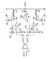
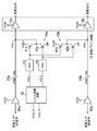
- FIG. 1 is a diagram illustrating a configuration of a signal potential conversion circuit according to a first embodiment. It is a structural example of the clamp circuit in FIG. It is a graph showing the change of the clamp electric potential accompanying the change of the power supply voltage of the input side in embodiment. It is an example of the structure which produces
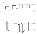
- FIG. (A), (b) is a signal waveform diagram for demonstrating a subject.
- FIG. 1 is a diagram illustrating a signal potential conversion circuit according to the first embodiment and a circuit configuration before and after the signal potential conversion circuit.
- the signal potential conversion circuit shown in FIG. 1 uses AC coupling.
- 10 is a receiving circuit that receives the signal IN of the termination node ND and generates an output signal OUT
- 20 is a capacitor to which the input signal CIN is applied at one end and the other end is connected to the termination node ND
- 30 A signal driving circuit for driving the input signal CIN
- a clamp circuit 40 for receiving the potential (signal IN) of the termination node ND.
- the capacitor 20 and the clamp circuit 40 constitute a signal potential conversion circuit according to this embodiment.
- the signal drive circuit 30 is supplied with the power supply voltage VDDL and outputs a signal CIN having an amplitude of VDDL.
- the receiving circuit 10 is applied with the power supply voltage VDDH, amplifies the potential of the signal IN with respect to the reference potential VTT, and generates an output signal OUT having an amplitude of VDDH.
- the signal IN needs to have an amplitude centered on the reference potential VTT.
- the clamp circuit 40 has a function of changing the signal potential so that the signal IN becomes a signal having an amplitude around the reference potential VTT. That is, the clamp circuit 40 increases the potential of the signal IN when the signal IN is lower than the clamp potential VCL1 as the first potential, and the signal IN when the signal IN is higher than the clamp potential VCL2 as the second potential. (Where ground potential ⁇ VCL1 ⁇ VCL2 ⁇ VDDH). Thereby, the signal IN can be reliably shifted in the range from the potential VCL1 to the potential VCL2. For this reason, the level of the input signal CIN can be reliably converted without changing the data width.
- the drain is connected to the power supply VDDH as the first power supply, the source is connected to the termination node ND, and the drain is connected to the ground power supply as the second power supply.
- a PMOS transistor 42 having a source connected to the termination node ND. That is, the NMOS transistor 41 as the first connection element and the PMOS transistor 42 as the second connection element each terminate the input node of the reception circuit 10.
- the clamp circuit 40 includes a control potential generation circuit 43 (indicated as NBG in the figure) that generates the gate potential NBIAS of the NMOS transistor 41 and a control potential generation circuit 44 (in the figure, PBG) that generates the gate potential PBIAS of the PMOS transistor 42. And a level adjustment circuit 50 for adjusting the levels of the potentials VCL1 and VCL2.
- the control potential generation circuit 43 receives the potential VCL1 output from the level adjustment circuit 50, and controls the gate potential NBIAS so that the NMOS transistor 41 becomes conductive when the potential of the termination node ND becomes lower than the potential VCL1.
- the control potential generation circuit 44 receives the potential VCL2 output from the level adjustment circuit 50, and controls the gate potential PBIAS so that the PMOS transistor 42 becomes conductive when the potential of the termination node ND becomes higher than the potential VCL2.
- the level adjustment circuit 50 adjusts the potentials VCL1 and VCL2 according to the level of the power supply voltage VDDL of the signal drive circuit 30 that drives the input signal CIN.
- Level adjustment circuit 50 receives power supply voltage VDD and a predetermined reference potential Vref.
- FIG. 2 shows a configuration example of the clamp circuit 40.
- the control potential generation circuit 43 is configured by the current source 45 and the NMOS transistor 46
- the control potential generation circuit 44 is configured by the current source 47 and the PMOS transistor 48.
- the level adjustment circuit 50 includes a comparator 51, current sources 53 and 56, and resistors 54 and 57.
- the current source 53 and the resistor 54 constitute a subtracting unit 52
- the current source 56 and the resistor 57 constitute an adding unit 55.
- the potential VCL1 output from the subtraction unit 52 is supplied to the control potential generation circuit 43 via the buffer 58
- the potential VCL2 output from the addition unit 55 is supplied to the control potential generation circuit 44 via the buffer 59. Yes.
- the buffer 58 and the buffer 59 output analog input voltages with low impedance, and the buffer 58 prevents an error from occurring in the potential VCL1 due to a current flowing from the control potential generation circuit 43 into the subtraction unit 52.
- the buffer 59 prevents the current from flowing from the adding section 55 to the control potential generating circuit 44 and causing an error in the potential VCL2.
- a current source that allows the same current as that of the current source 45 to flow from the output node of the subtractor 52 in the ground direction may be inserted.
- a current source that allows the same current as that of the current source 44 to flow from the power source to the output node of the adder 55 may be inserted.
- the current source 53 converts the potential VCLB serving as a reference for the potential VCL1 into a current.
- the current output from the current source 53 and the current output Iout (N) of the comparator 51 flow through the resistor 54, whereby the potential VCL1 is obtained.
- the current source 56 converts the potential VCLT, which is a reference for the potential VCL2, into a current.
- the current output from the current source 56 and the current output Iout (P) of the comparator 51 flow through the resistor 57, whereby the potential VCL2 is obtained.
- FIG. 3 is a graph showing a change in clamp potential accompanying a change in power supply voltage VDDL.
- the clamp potentials VCL1 and VCL2 are equal to the reference potentials VCLB and VCLT, respectively.
- the clamp potential VCL1 increases and the clamp potential VCL2 decreases. That is, when the amplitude of the input signal CIN decreases with the decrease of the power supply voltage VDDL, the potential difference between the clamp potentials VCL1 and VCL2 decreases accordingly.
- the clamp potential VCL1 decreases and the clamp potential VCL2 increases.
- the degree of follow-up of the clamp potentials VCL1 and VCL2 can be adjusted by, for example, the resistance value Rin of the built-in resistor of the comparator 51.
- the clamp circuit 40 defines the potential of the termination node ND within the range from the potential VCL1 to the potential VCL2.
- the potentials VCL1 and VCL2 are adjusted by the level adjustment circuit 50 according to the power supply voltage VDDL of the circuit 30 that drives the input signal CIN. Therefore, even when the power supply voltage VDDL of the circuit 30 that drives the input signal CIN varies and the amplitude of the input signal CIN varies, the clamp potentials VCL1 and VCL2 can be dynamically adjusted accordingly. it can. Therefore, it is possible to suppress the occurrence of jitter in the converted signal OUT.
- the current values of the current sources 53 and 56 and the reference potential Vref are realized by a circuit configuration as shown in FIG. 4, for example.
- a band gap reference circuit 61 (denoted as “BGR” in the figure) generates and outputs a reference voltage Vbgr.
- a reference current having a current value Vbgr / R is generated based on the reference voltage Vbgr by a feedback loop including the operational amplifier 62, the transistor P1, and the resistor 63.
- the current mirror ratio of the transistor P4 to the transistor P1 is Vgbr: Vref
- the reference potential Vref is generated.
- the current mirror ratio may be 1: 1, and the resistance value of the resistor 64 may be R ⁇ (Vref / Vbgr).
- the termination node ND is terminated using the NMOS transistor 41 and the PMOS transistor 42.
- the present invention is not limited to this. That is, any connection element whose impedance decreases when the potential of the termination node ND becomes lower than VCL1 can be used in place of the NMOS transistor 41, and when the potential of the termination node ND becomes higher than VCL2. Any connection element that reduces the impedance can be used in place of the PMOS transistor 42.
- FIG. 5 is a diagram illustrating a signal potential conversion circuit according to the second embodiment and a circuit configuration before and after the signal potential conversion circuit.
- reception circuits 15a and 15b, capacitors 20a and 20b, signal drive circuits 30a and 30b, and clamp circuits 40a and 40b are provided for each of the positive signal and the negative signal constituting the differential signal.
- the differential driver circuit 15 is configured by the receiving circuits 15a and 15b.
- the capacitors 20a and 20b and the clamp circuits 40a and 40b constitute a signal potential conversion circuit according to this embodiment.
- the signal drive circuits 30a and 30b are supplied with a power supply voltage VDDL and output signals CINa and CINb having an amplitude of VDDL.
- the differential driver circuit 15 is applied with the power supply voltage VDDH, amplifies the potentials of the signals INa and INb, and generates a differential signal having an amplitude of VDDH.
- the clamp circuit 40a raises the potential of the signal INa when the signal INa falls below the potential VCL1, and lowers the potential of the signal INa when the signal INa rises above the potential VCL2.
- the clamp circuit 40b increases the potential of the signal INb when the signal INb is lower than the potential VCL1, and decreases the potential of the signal INb when the signal INb is higher than the potential VCL2.
- the clamp circuit 40a has a drain connected to a power supply VDDH as a first power supply, a source connected to the termination node NDa, an NMOS transistor 41a as a first connection element, and a drain connected to a second power supply VDDH. And a PMOS transistor 42a as a second connection element having a source connected to the termination node NDa.
- the clamp circuit 40b has a drain connected to a power supply VDDH serving as a first power supply, an NMOS transistor 41b serving as a first connection element having a source connected to a termination node NDb, and a drain connected to a power supply VDDH.
- a PMOS transistor 42b as a second connection element having a source connected to a ground power source as a second power source and a source connected to the termination node NDb is provided. Further, the clamp circuits 40a and 40b share a control potential generation circuit 43 that generates the gate potentials of the NMOS transistors 41a and 41b and a control potential generation circuit 44 that generates the gate potentials of the PMOS transistors 42a and 42b.
- the clamp circuits 40a and 40b share a level adjustment circuit 50 that adjusts the levels of the potentials VCL1 and VCL2.
- the control potential generation circuit 43 receives the potential VCL1 output from the level adjustment circuit 50, and controls the gate potential so that the NMOS transistors 41a and 41b are turned on when the potentials of the termination nodes NDa and NDb fall below the potential VCL1.
- the control potential generation circuit 44 receives the potential VCL2 output from the level adjustment circuit 50, and controls the gate potential so that the PMOS transistors 42a and 42b become conductive when the potentials of the termination nodes NDa and NDb exceed the potential VCL2. .
- the level adjustment circuit 50 adjusts the potentials VCL1 and VCL2 according to the level of the power supply potential VDDL of the signal drive circuits 30a and 30b that drive the input signals CINa and CINb.
- Level adjustment circuit 50 receives power supply potential VDD and predetermined reference potential Vref.
- the specific configuration and operation of the level adjustment circuit 50 are the same as those in the first embodiment, and a description thereof is omitted here.
- the clamp circuits 40a and 40b define the potentials of the termination nodes NDa and NDb within a range from the potential VCL1 to the potential VCL2.
- the potentials VCL1 and VCL2 are adjusted by the level adjustment circuit 50 according to the power supply voltage VDDL of the circuits 30a and 30b that drive the input signals CINa and CINb. Therefore, even when the power supply voltage VDDL of the circuits 30a and 30b for driving the input signals CINa and CINb varies and the amplitude of the input signals CINa and CINb varies, the clamp potentials VCL1 and VCL2 are moved accordingly. Can be adjusted. Therefore, it is possible to suppress the occurrence of jitter in the differential output after conversion.
- control potential generation circuits 43 and 44 and the level adjustment circuit 50 may be provided in each of the clamp circuits 40a and 40b, but the circuit scale can be reduced by sharing as shown in FIG.
- the termination nodes NDa and NDb are terminated using the NMOS transistors 41a and 41b and the PMOS transistors 42a and 42b.
- the present invention is not limited to this. That is, any connection element whose impedance is lowered when the potentials of the termination nodes NDa and NDb are lower than VCL1 can be used in place of the NMOS transistors 41a and 41b. As long as the connection element has a lower impedance when it becomes higher, it can be used in place of the PMOS transistors 42a and 42b.
- the level adjustment circuit 50 adjusts both the clamp potentials VCL1 and VCL2 according to the power supply voltage VDDL. For example, one of the clamp potentials VCL1 and VCL2 is adjusted. Adjustment may be made according to the power supply voltage VDDL, and the other may be fixed.
- the signal potential conversion circuit according to the present disclosure is effective for use in, for example, a high-speed interface circuit because the clamp potential can be dynamically adjusted according to the power supply voltage on the input side.
Landscapes
- Engineering & Computer Science (AREA)
- Computer Hardware Design (AREA)
- Physics & Mathematics (AREA)
- Computing Systems (AREA)
- General Engineering & Computer Science (AREA)
- Mathematical Physics (AREA)
- Nonlinear Science (AREA)
- Logic Circuits (AREA)
Abstract
信号電位変換回路において、コンデンサ(20)は入力信号(CIN)が一端に与えられ、他端が終端ノード(ND)と接続されている。クランプ回路(40)は終端ノード(ND)の電位(信号IN)を、電位VCL1からVCL2までの範囲に規定する。クランプ回路(40)は、電位VCL1,VCL2のうち少なくともいずれか一方を、入力信号(CIN)を駆動する回路(30)の電源電位VDDLに応じて調整するレベル調整回路(50)を備えている。
Description
本開示は、異電位信号の受け渡しのために、入力信号の電位を変換する信号電位変換回路に関する。
最近のトランジスタは、微細化に伴い、動作電圧の低電圧化が進んでいる。一方、外部インターフェースに関しては電圧規格が決まっており、集積回路は、旧来のデバイスとも接続できるように、例えば5Vや3.3Vで動作させなければならない。このため、微細トランジスタで駆動される信号と例えば5Vや3.3Vで駆動される信号とのやりとりのために、レベルシフト回路(信号電位変換回路)が用いられる。特に、高速信号の伝達のためには、コンデンサを用いたAC結合回路が有効である。
特許文献1には、信号電位変換回路について、変換後の信号にジッタが発生しないように、終端ノードの電位の変動を抑制する構成が開示されている。
特許文献1の構成では、AC結合後の終端ノードにおける信号に対して、上限電位と下限電位を設定し、クランプをかけている。このような構成では、クランプ電位差と信号の振幅とが一致しない場合には、変換後の信号にジッタが発生しやすくなる。
例えば、図6(a)に示すように、信号振幅がクランプ電位差(VCLT-VCLB)に比べて小さい場合は、信号レベルが安定しない。また、図6(b)に示すように、信号振幅がクランプ電位差(VCLT-VCLB)よりも大きい場合は、信号波形に歪みが生じる。いずれの場合も、変換後の信号にジッタが生じる原因になる。
このような課題を解決するためには、クランプ電位差を信号振幅に合わせればよい。ただし、信号振幅は、入力信号を生成する回路部分の電源電圧の影響を受ける。このため、入力側の電源電圧に応じて、クランプ電位を動的に調整する構成が必要になる。
本開示は、入力側の電源電圧に応じてクランプ電位を動的に調整可能な構成を有する信号電位変換回路を提供する。
本開示の一態様では、信号電位変換回路は、入力信号が一端に与えられ、他端が終端ノードと接続されたコンデンサと、終端ノードの電位を受けるクランプ回路とを備え、クランプ回路は、第1の電源と終端ノードとの間に設けられた第1の接続素子と、終端ノードと、電源電圧が第1の電源よりも低い第2の電源との間に設けられた第2の接続素子とを備え、第1の接続素子は、終端ノードの電位が、第2の電源の電源電圧よりも高い第1の電位よりも低くなったとき、インピーダンスが低下するものであり、第2の接続素子は、終端ノードの電位が、第1の電源の電源電圧よりも低く、かつ、第1の電位よりも高い第2の電位よりも高くなったとき、インピーダンスが低下するものであり、クランプ回路は、第1の電位および前記第2の電位のうち少なくともいずれか一方を、入力信号を駆動する回路の電源電圧に応じて、調整するレベル調整回路を備えている。
この態様によると、クランプ回路によって、終端ノードの電位が第1の電位から第2の電位までの範囲に規定される。また、第1の電位および第2の電位のうち少なくともいずれか一方は、レベル調整回路によって、入力信号を駆動する回路の電源電圧に応じて調整される。このため、入力信号を駆動する回路の電源電圧が変動し、入力信号の振幅が変動した場合であっても、これに応じてクランプ電位を動的に調整することができる。したがって、変換後の信号にジッタが発生することを抑制することができる。
本開示によると、入力側の電源電圧に応じてクランプ電位を動的に調整可能な構成を有する信号電位変換回路を提供することができる。
以下の実施形態では、特に問題のない限りにおいて、電源とその電源電圧について同一の符号を用いて説明を行っている。
(実施形態1)
図1は実施形態1に係る信号電位変換回路とその前後の回路構成を示す図である。図1に示す信号電位変換回路はAC結合を利用したものである。図1において、10は終端ノードNDの信号INを受信し、出力信号OUTを生成する受信回路、20は入力信号CINが一端に与えられるとともに他端が終端ノードNDと接続されたコンデンサ、30は入力信号CINを駆動する信号駆動回路、40は終端ノードNDの電位(信号IN)を受けるクランプ回路である。コンデンサ20およびクランプ回路40によって、本実施形態に係る信号電位変換回路が構成されている。
図1は実施形態1に係る信号電位変換回路とその前後の回路構成を示す図である。図1に示す信号電位変換回路はAC結合を利用したものである。図1において、10は終端ノードNDの信号INを受信し、出力信号OUTを生成する受信回路、20は入力信号CINが一端に与えられるとともに他端が終端ノードNDと接続されたコンデンサ、30は入力信号CINを駆動する信号駆動回路、40は終端ノードNDの電位(信号IN)を受けるクランプ回路である。コンデンサ20およびクランプ回路40によって、本実施形態に係る信号電位変換回路が構成されている。
信号駆動回路30は、電源電圧VDDLが印加されており、振幅がVDDLである信号CINを出力する。受信回路10は、電源電圧VDDHが印加されており、基準電位VTTに対する信号INの電位を増幅して、振幅がVDDHの出力信号OUTを生成する。受信回路10が適正に動作するためには、信号INが基準電位VTTを中心にして振幅している必要がある。
クランプ回路40は、信号INが基準電位VTTを中心にして振幅する信号になるように、信号電位の変更を行う機能を有する。すなわち、クランプ回路40は、信号INが第1の電位としてのクランプ電位VCL1を下回ったときは信号INの電位を上げ、信号INが第2の電位としてのクランプ電位VCL2を上回ったときは信号INの電位を下げる(ただし、接地電位<VCL1<VCL2<VDDH)。これにより、信号INを電位VCL1から電位VCL2の範囲で確実に遷移させることができる。このため、入力信号CINを、そのデータ幅を変化させることなく、確実にレベル変換することが可能となる。
クランプ回路40は具体的には、ドレインが第1の電源としての電源VDDHに接続されるとともに、ソースが終端ノードNDに接続されたNMOSトランジスタ41と、ドレインが第2の電源としての接地電源に接続されるとともに、ソースが終端ノードNDに接続されたPMOSトランジスタ42とを備えている。すなわち、第1の接続素子としてのNMOSトランジスタ41、および第2の接続素子としてのPMOSトランジスタ42がそれぞれ、受信回路10の入力ノードを終端している。
また、クランプ回路40は、NMOSトランジスタ41のゲート電位NBIASを生成する制御電位発生回路43(図ではNBGと表記)と、PMOSトランジスタ42のゲート電位PBIASを生成する制御電位発生回路44(図ではPBGと表記)と、電位VCL1,VCL2のレベルを調整するレベル調整回路50とを備えている。制御電位発生回路43はレベル調整回路50から出力された電位VCL1を受け、終端ノードNDの電位が電位VCL1よりも低くなったときにNMOSトランジスタ41が導通するように、ゲート電位NBIASを制御する。制御電位発生回路44はレベル調整回路50から出力された電位VCL2を受け、終端ノードNDの電位が電位VCL2よりも高くなったときにPMOSトランジスタ42が導通するように、ゲート電位PBIASを制御する。
レベル調整回路50は、入力信号CINを駆動する信号駆動回路30の電源電圧VDDLのレベルに応じて、電位VCL1,VCL2を調整する。レベル調整回路50は、電源電圧VDDと、所定の参照電位Vrefとを受ける。
図2はクランプ回路40の構成例である。図2の構成では、電流源45およびNMOSトランジスタ46によって制御電位発生回路43が構成されており、電流源47およびPMOSトランジスタ48によって制御電位発生回路44が構成されている。レベル調整回路50は、比較器51と、電流源53,56と、抵抗54,57とを備えている。電流源53および抵抗54によって減算部52が構成されており、電流源56および抵抗57によって加算部55が構成されている。減算部52から出力された電位VCL1はバッファ58を介して制御電位発生回路43に与えられており、加算部55から出力された電位VCL2はバッファ59を介して制御電位発生回路44に与えられている。
なお、バッファ58とバッファ59はアナログ入力電圧を低インピーダンスで出力するものであり、バッファ58は制御電位発生回路43から減算部52に電流が流入して電位VCL1に誤差が生じるのを防止しており、バッファ59は加算部55から制御電位発生回路44に電流が流出して電位VCL2に誤差が生じるのを防止している。バッファ58を挿入する代わりに、電流源45と同じ電流を減算部52の出力ノードから接地方向に流す電流源を入れても良い。また、バッファ59を挿入する代わりに、電流源44と同じ電流を電源から加算部55の出力ノードに流す電流源を入れても良い。
比較部としての比較器51は、電源電圧VDDLと参照電位Vrefとを受ける。そして、電源電圧VDDLと参照電位Vrefとの電位差すなわちΔVDDL(=VDDL-Vref)を内蔵抵抗によって電流に変換し、出力する。内蔵抵抗の抵抗値をRinとすると、比較器51の2個の電流出力Iout(N),Iout(P)は、
Iout(N)=-ΔVDDL/Rin
Iout(P)=ΔVDDL/Rin
となる。減算部52において、電流源53は電位VCL1の基準となる電位VCLBを電流に変換している。抵抗54に電流源53から出力された電流と比較器51の電流出力Iout(N)とが流れ、これにより電位VCL1が得られる。電流源53の電流値をVCLB/R、抵抗54の抵抗値をRとすると、
VCL1=R×(VCLB/R+Iout(N))
=VCLB-ΔVDDL×(R/Rin)
となる。また、加算部55において、電流源56は電位VCL2の基準となる電位VCLTを電流に変換している。抵抗57に電流源56から出力された電流と比較器51の電流出力Iout(P)とが流れ、これにより電位VCL2が得られる。電流源56の電流値をVCLT/R、抵抗57の抵抗値をRとすると、
VCL2=R×(VCLT/R+Iout(P))
=VCLT+ΔVDDL×(R/Rin)
となる。
Iout(N)=-ΔVDDL/Rin
Iout(P)=ΔVDDL/Rin
となる。減算部52において、電流源53は電位VCL1の基準となる電位VCLBを電流に変換している。抵抗54に電流源53から出力された電流と比較器51の電流出力Iout(N)とが流れ、これにより電位VCL1が得られる。電流源53の電流値をVCLB/R、抵抗54の抵抗値をRとすると、
VCL1=R×(VCLB/R+Iout(N))
=VCLB-ΔVDDL×(R/Rin)
となる。また、加算部55において、電流源56は電位VCL2の基準となる電位VCLTを電流に変換している。抵抗57に電流源56から出力された電流と比較器51の電流出力Iout(P)とが流れ、これにより電位VCL2が得られる。電流源56の電流値をVCLT/R、抵抗57の抵抗値をRとすると、
VCL2=R×(VCLT/R+Iout(P))
=VCLT+ΔVDDL×(R/Rin)
となる。
図3は電源電圧VDDLの変化に伴うクランプ電位の変化を表すグラフである。図3に示すように、電源電圧VDDLが参照電位Vrefと等しいときは、クランプ電位VCL1,VCL2はそれぞれ、基準となる電位VCLB,VCLTと等しくなる。電源電圧VDDLが低下すると、クランプ電位VCL1は上昇し、クランプ電位VCL2は低下する。すなわち、電源電圧VDDLの低下に伴って入力信号CINの振幅が小さくなったとき、クランプ電位VCL1,VCL2の電位差が、これに追従して小さくなる。また、電源電圧VDDLが上昇すると、クランプ電位VCL1は低下し、クランプ電位VCL2は上昇する。すなわち、電源電圧VDDLの上昇に伴って入力信号CINの振幅が大きくなったとき、クランプ電位VCL1,VCL2の電位差が、これに追従して大きくなる。なお、クランプ電位VCL1,VCL2の追従の程度は、例えば、比較器51の内蔵抵抗の抵抗値Rinによって調整することができる。
このように本実施形態によると、クランプ回路40によって、終端ノードNDの電位が電位VCL1から電位VCL2までの範囲に規定される。また、電位VCL1,VCL2は、レベル調整回路50によって、入力信号CINを駆動する回路30の電源電圧VDDLに応じて調整される。このため、入力信号CINを駆動する回路30の電源電圧VDDLが変動し、入力信号CINの振幅が変動した場合であっても、これに応じてクランプ電位VCL1,VCL2を動的に調整することができる。したがって、変換後の信号OUTにジッタが発生することを抑制することができる。
なお、本実施形態におけるレベル調整回路50において、電流源53,56の電流値や、参照電位Vrefは、例えば図4のような回路構成によって実現される。図4において、バンドギャップリファレンス回路61(図では「BGR」と表記)は、基準電圧Vbgrを生成出力する。オペアンプ62、トランジスタP1および抵抗63によるフィードバックループによって、基準電圧Vbgrを基にして、電流値Vbgr/Rの基準電流が生成される。
トランジスタP2は、トランジスタP1とのカレントミラー比が、Vgbr:VCLBであるので、流れる電流の電流値は、VCLB/R(=(Vgbr/R)×(VCLB/Vbgr))となる。すなわち、電流源53が実現される。また、トランジスタP3は、トランジスタP1とのカレントミラー比が、Vgbr:VCLTであるので、流れる電流の電流値は、VCLT/R(=(Vbgr/R)×(VCLT/Vbgr))となる。すなわち、電流源56が実現される。
さらに、トランジスタP4は、トランジスタP1とのカレントミラー比が、Vgbr:Vrefであるので、流れる電流の電流値は、Vref/R(=(Vbgr/R)×(Vref/Vgbr))となる。この電流が抵抗64(抵抗値R)を流れることによって、参照電位Vrefが生成される。なお例えば、カレントミラー比を1:1とし、抵抗64の抵抗値をR×(Vref/Vbgr)としてもよい。
なお、本実施形態では、NMOSトランジスタ41およびPMOSトランジスタ42を用いて終端ノードNDを終端するものとしたが、これに限られるものではない。すなわち、終端ノードNDの電位がVCL1よりも低くなったときインピーダンスが低下する接続素子であれば、NMOSトランジスタ41の代わりに用いることができるし、終端ノードNDの電位がVCL2よりも高くなったときインピーダンスが低下する接続素子であれば、PMOSトランジスタ42の代わりに用いることができる。
(実施形態2)
実施形態1では、信号が単相信号(シングルエンド)であるものとして説明を行った。本開示内容は、差動信号をレベル変換する構成にも適用可能である。
実施形態1では、信号が単相信号(シングルエンド)であるものとして説明を行った。本開示内容は、差動信号をレベル変換する構成にも適用可能である。
図5は実施形態2に係る信号電位変換回路とその前後の回路構成を示す図である。図5の構成では、差動信号を構成する正信号および負信号のそれぞれについて、受信回路15a,15b、コンデンサ20a,20b、信号駆動回路30a,30b、およびクランプ回路40a,40bが設けられている。受信回路15a,15bによって、差動ドライバ回路15が構成されている。コンデンサ20a,20b、クランプ回路40a,40bによって、本実施形態に係る信号電位変換回路が構成されている。
信号駆動回路30a,30bは、電源電圧VDDLが印加されており、振幅がVDDLである信号CINa,CINbを出力する。差動ドライバ回路15は、電源電圧VDDHが印加されており、信号INa,INbの電位を増幅して、振幅がVDDHの差動信号を生成する。
クランプ回路40aは、信号INaが電位VCL1を下回ったときは信号INaの電位を上げ、信号INaが電位VCL2を上回ったときは信号INaの電位を下げる。同様に、クランプ回路40bは、信号INbが電位VCL1を下回ったときは信号INbの電位を上げ、信号INbが電位VCL2を上回ったときは信号INbの電位を下げる。
クランプ回路40aは具体的には、ドレインが第1の電源としての電源VDDHに接続されるとともに、ソースが終端ノードNDaに接続された第1の接続素子としてのNMOSトランジスタ41aと、ドレインが第2の電源としての接地電源に接続されるとともに、ソースが終端ノードNDaに接続された第2の接続素子としてのPMOSトランジスタ42aとを備えている。また、クランプ回路40bは具体的には、ドレインが第1の電源としての電源VDDHに接続されるとともに、ソースが終端ノードNDbに接続された第1の接続素子としてのNMOSトランジスタ41bと、ドレインが第2の電源としての接地電源に接続されるとともに、ソースが終端ノードNDbに接続された第2の接続素子としてのPMOSトランジスタ42bとを備えている。さらに、クランプ回路40a,40bは、NMOSトランジスタ41a,41bのゲート電位を生成する制御電位発生回路43と、PMOSトランジスタ42a,42bのゲート電位を生成する制御電位発生回路44とを共有している。
そしてクランプ回路40a,40bは、電位VCL1,VCL2のレベルを調整するレベル調整回路50を共有している。制御電位発生回路43はレベル調整回路50から出力された電位VCL1を受け、終端ノードNDa,NDbの電位が電位VCL1を下回ったときにNMOSトランジスタ41a,41bが導通するように、ゲート電位を制御する。制御電位発生回路44はレベル調整回路50から出力された電位VCL2を受け、終端ノードNDa,NDbの電位が電位VCL2を上回ったときにPMOSトランジスタ42a,42bが導通するように、ゲート電位を制御する。レベル調整回路50は、入力信号CINa,CINbを駆動する信号駆動回路30a,30bの電源電位VDDLのレベルに応じて、電位VCL1,VCL2を調整する。レベル調整回路50は、電源電位VDDと、所定の参照電位Vrefとを受ける。なお、レベル調整回路50の具体的な構成と動作については、実施形態1と同様であるため、ここではその説明を省略する。
本実施形態においても、実施形態1と同様の作用効果が得られる。すなわち、クランプ回路40a,40bによって、終端ノードNDa,NDbの電位が電位VCL1から電位VCL2までの範囲に規定される。また、電位VCL1,VCL2は、レベル調整回路50によって、入力信号CINa,CINbを駆動する回路30a,30bの電源電圧VDDLに応じて調整される。このため、入力信号CINa,CINbを駆動する回路30a,30bの電源電圧VDDLが変動し、入力信号CINa,CINbの振幅が変動した場合であっても、これに応じてクランプ電位VCL1,VCL2を動的に調整することができる。したがって、変換後の差動出力にジッタが発生することを抑制することができる。
なお、制御電位発生回路43,44およびレベル調整回路50は、クランプ回路40a,40bのそれぞれに設けてもかまわないが、図5のように共有することによって、回路規模を小さくすることができる。
なお、本実施形態では、NMOSトランジスタ41a,41bおよびPMOSトランジスタ42a,42bを用いて終端ノードNDa,NDbを終端するものとしたが、これに限られるものではない。すなわち、終端ノードNDa,NDbの電位がVCL1よりも低くなったときインピーダンスが低下する接続素子であれば、NMOSトランジスタ41a,41bの代わりに用いることができるし、終端ノードNDa,NDbの電位がVCL2よりも高くなったときインピーダンスが低下する接続素子であれば、PMOSトランジスタ42a,42bの代わりに用いることができる。
なお、上述の各実施形態1,2では、レベル調整回路50は、クランプ電位VCL1,VCL2の両方を、電源電圧VDDLに応じて調整するものとしたが、例えば、クランプ電位VCL1,VCL2の一方を電源電圧VDDLに応じて調整し、他方を固定値としてもかまわない。
本開示に係る信号電位変換回路では、入力側の電源電圧に応じてクランプ電位を動的に調整可能なので、例えば、高速インターフェース回路に用いるのに有効である。
CIN,CINa,CINb 入力信号
ND,NDa,NDb 終端ノード
VCL1 第1の電位
VCL2 第2の電位
VDDL 入力信号を駆動する回路の電源電圧
Vref 参照電位
20,20a,20b コンデンサ
40,40a,40b クランプ回路
41,41a,41b NMOSトランジスタ(第1の接続素子)
42,42a,42b PMOSトランジスタ(第2の接続素子)
43 制御電位生成回路
44 制御電位生成回路
50 レベル調整回路
51 比較器(比較部)
52 減算部
55 加算部
ND,NDa,NDb 終端ノード
VCL1 第1の電位
VCL2 第2の電位
VDDL 入力信号を駆動する回路の電源電圧
Vref 参照電位
20,20a,20b コンデンサ
40,40a,40b クランプ回路
41,41a,41b NMOSトランジスタ(第1の接続素子)
42,42a,42b PMOSトランジスタ(第2の接続素子)
43 制御電位生成回路
44 制御電位生成回路
50 レベル調整回路
51 比較器(比較部)
52 減算部
55 加算部
Claims (5)
- 入力信号が一端に与えられ、他端が終端ノードと接続されたコンデンサと、
前記終端ノードの電位を受けるクランプ回路とを備え、
前記クランプ回路は、
第1の電源と前記終端ノードとの間に設けられた第1の接続素子と、
前記終端ノードと、電源電圧が前記第1の電源よりも低い第2の電源との間に設けられた第2の接続素子とを備え、
前記第1の接続素子は、前記終端ノードの電位が、前記第2の電源の電源電圧よりも高い第1の電位よりも低くなったとき、インピーダンスが低下するものであり、
前記第2の接続素子は、前記終端ノードの電位が、前記第1の電源の電源電圧よりも低く、かつ、前記第1の電位よりも高い第2の電位よりも高くなったとき、インピーダンスが低下するものであり、
前記クランプ回路は、前記第1の電位および前記第2の電位のうち少なくともいずれか一方を、前記入力信号を駆動する回路の電源電圧に応じて、調整するレベル調整回路を備えている
ことを特徴とする信号電位変換回路。 - 請求項1記載の信号電位変換回路において、
前記レベル調整回路は、
前記入力信号を駆動する回路の電源電圧と、所定の参照電位との電位差を、電流に変換して出力する比較部と、
前記第1の電位の基準となる電位を電流に変換し、この電流から前記比較部の出力電流を減じ、減じた後の電流を電圧に変換して出力する減算部とを備え、
前記減算部の出力電圧が、前記第1の電位として用いられる
ことを特徴とする信号電位変換回路。 - 請求項2記載の信号電位変換回路において、
前記クランプ回路は、
前記第1の接続素子として、ドレインが前記第1の電源に接続されるとともに、ソースが前記終端ノードに接続されたNMOSトランジスタを備えており、かつ、
前記減算部の出力電圧を基にして、前記NMOSトランジスタのゲートに与える制御電位を生成する制御電位発生回路を備えている
ことを特徴とする信号電位変換回路。 - 請求項1記載の信号電位変換回路において、
前記レベル調整回路は、
前記入力信号を駆動する回路の電源電圧と、所定の参照電位との電位差を、電流に変換して出力する比較部と、
前記第2の電位の基準となる電位を電流に変換し、この電流に前記比較部の出力電流を加え、加えた後の電流を電圧に変換して出力する加算部とを備え、
前記加算部の出力電圧が、前記第2の電位として用いられる
ことを特徴とする信号電位変換回路。 - 請求項4記載の信号電位変換回路において、
前記クランプ回路は、
前記第2の接続素子として、ドレインが前記第2の電源に接続されるとともに、ソースが前記終端ノードに接続されたPMOSトランジスタを備えており、かつ、
前記加算部の出力電圧を基にして、前記PMOSトランジスタのゲートに与える制御電位を生成する制御電位発生回路を備えている
ことを特徴とする信号電位変換回路。
Priority Applications (2)
| Application Number | Priority Date | Filing Date | Title |
|---|---|---|---|
| JP2015554541A JP6455443B2 (ja) | 2013-12-25 | 2014-12-16 | 信号電位変換回路 |
| US15/191,455 US9584103B2 (en) | 2013-12-25 | 2016-06-23 | Signal potential converter |
Applications Claiming Priority (2)
| Application Number | Priority Date | Filing Date | Title |
|---|---|---|---|
| JP2013267931 | 2013-12-25 | ||
| JP2013-267931 | 2013-12-25 |
Related Child Applications (1)
| Application Number | Title | Priority Date | Filing Date |
|---|---|---|---|
| US15/191,455 Continuation US9584103B2 (en) | 2013-12-25 | 2016-06-23 | Signal potential converter |
Publications (1)
| Publication Number | Publication Date |
|---|---|
| WO2015098041A1 true WO2015098041A1 (ja) | 2015-07-02 |
Family
ID=53477946
Family Applications (1)
| Application Number | Title | Priority Date | Filing Date |
|---|---|---|---|
| PCT/JP2014/006271 Ceased WO2015098041A1 (ja) | 2013-12-25 | 2014-12-16 | 信号電位変換回路 |
Country Status (3)
| Country | Link |
|---|---|
| US (1) | US9584103B2 (ja) |
| JP (1) | JP6455443B2 (ja) |
| WO (1) | WO2015098041A1 (ja) |
Families Citing this family (1)
| Publication number | Priority date | Publication date | Assignee | Title |
|---|---|---|---|---|
| JP6561842B2 (ja) * | 2013-12-25 | 2019-08-21 | 株式会社ソシオネクスト | 信号電位変換回路 |
Citations (3)
| Publication number | Priority date | Publication date | Assignee | Title |
|---|---|---|---|---|
| JP2000091902A (ja) * | 1998-09-16 | 2000-03-31 | Nec Corp | インタフェース回路及びこれを含む入力バッファ集積回路 |
| JP2009044304A (ja) * | 2007-08-07 | 2009-02-26 | Denso Corp | 半導体素子制御装置 |
| WO2012157031A1 (ja) * | 2011-05-13 | 2012-11-22 | パナソニック株式会社 | 信号電位変換回路 |
Family Cites Families (4)
| Publication number | Priority date | Publication date | Assignee | Title |
|---|---|---|---|---|
| US7023497B2 (en) * | 2002-07-31 | 2006-04-04 | Texas Instruments Incorporated | Clamping circuit with wide input dynamic range for video or other AC coupled signals |
| TWI520485B (zh) * | 2010-09-06 | 2016-02-01 | 晨星半導體股份有限公司 | 耐受高電壓之輸出入電路與相關裝置 |
| US8692605B2 (en) * | 2011-06-27 | 2014-04-08 | Mediatek Inc. | Receiving circuits for core circuits |
| JP6561842B2 (ja) * | 2013-12-25 | 2019-08-21 | 株式会社ソシオネクスト | 信号電位変換回路 |
-
2014
- 2014-12-16 JP JP2015554541A patent/JP6455443B2/ja active Active
- 2014-12-16 WO PCT/JP2014/006271 patent/WO2015098041A1/ja not_active Ceased
-
2016
- 2016-06-23 US US15/191,455 patent/US9584103B2/en active Active
Patent Citations (3)
| Publication number | Priority date | Publication date | Assignee | Title |
|---|---|---|---|---|
| JP2000091902A (ja) * | 1998-09-16 | 2000-03-31 | Nec Corp | インタフェース回路及びこれを含む入力バッファ集積回路 |
| JP2009044304A (ja) * | 2007-08-07 | 2009-02-26 | Denso Corp | 半導体素子制御装置 |
| WO2012157031A1 (ja) * | 2011-05-13 | 2012-11-22 | パナソニック株式会社 | 信号電位変換回路 |
Also Published As
| Publication number | Publication date |
|---|---|
| US9584103B2 (en) | 2017-02-28 |
| JP6455443B2 (ja) | 2019-01-23 |
| JPWO2015098041A1 (ja) | 2017-03-23 |
| US20160308518A1 (en) | 2016-10-20 |
Similar Documents
| Publication | Publication Date | Title |
|---|---|---|
| US20100231266A1 (en) | Low voltage and low power differential driver with matching output impedances | |
| US20120049960A1 (en) | Pre-driver and digital transmitter using the same | |
| US20100271102A1 (en) | Semiconductor integrated circuit | |
| US7304540B2 (en) | Source follower and current feedback circuit thereof | |
| JP4798618B2 (ja) | 出力回路および半導体集積回路装置 | |
| TWI448868B (zh) | Voltage regulator | |
| US20110304399A1 (en) | Driver amplifier circuit and communication system | |
| JP4097149B2 (ja) | 差動駆動回路およびそれを内蔵する電子機器 | |
| CN101741373B (zh) | 一种自适应多种io电源的低电压差分信号驱动器 | |
| US8866550B2 (en) | Amplifier circuit with overshoot suppression | |
| JP4614234B2 (ja) | 電源装置およびそれを備える電子機器 | |
| US10972079B2 (en) | Common mode voltage level shifting and locking circuit | |
| JP6455443B2 (ja) | 信号電位変換回路 | |
| US11290061B2 (en) | Amplifier circuit with overshoot suppression | |
| TWI612771B (zh) | 具有用於傳輸信號之可組態可變供應電壓之介面電路 | |
| CN101483425B (zh) | 低功率差动信号传输装置 | |
| JP2008301083A (ja) | 差動信号生成回路 | |
| TWI528369B (zh) | 參考供應電壓產生裝置 | |
| JP6561842B2 (ja) | 信号電位変換回路 | |
| JP2018019223A (ja) | シングル差動変換回路 | |
| JP5203809B2 (ja) | 電流ミラー回路 | |
| US9337789B2 (en) | Differential receiver | |
| JP2015061187A (ja) | 光受信回路 | |
| JP2007006136A (ja) | インタフェイス回路 |
Legal Events
| Date | Code | Title | Description |
|---|---|---|---|
| 121 | Ep: the epo has been informed by wipo that ep was designated in this application |
Ref document number: 14874346 Country of ref document: EP Kind code of ref document: A1 |
|
| ENP | Entry into the national phase |
Ref document number: 2015554541 Country of ref document: JP Kind code of ref document: A |
|
| NENP | Non-entry into the national phase |
Ref country code: DE |
|
| 122 | Ep: pct application non-entry in european phase |
Ref document number: 14874346 Country of ref document: EP Kind code of ref document: A1 |