WO2015093396A1 - Dispositif d'éclairage et dispositif d'affichage - Google Patents
Dispositif d'éclairage et dispositif d'affichage Download PDFInfo
- Publication number
- WO2015093396A1 WO2015093396A1 PCT/JP2014/082932 JP2014082932W WO2015093396A1 WO 2015093396 A1 WO2015093396 A1 WO 2015093396A1 JP 2014082932 W JP2014082932 W JP 2014082932W WO 2015093396 A1 WO2015093396 A1 WO 2015093396A1
- Authority
- WO
- WIPO (PCT)
- Prior art keywords
- light
- surface side
- guide plate
- prism
- side unit
- Prior art date
Links
Images


Classifications
-
- G—PHYSICS
- G02—OPTICS
- G02B—OPTICAL ELEMENTS, SYSTEMS OR APPARATUS
- G02B6/00—Light guides; Structural details of arrangements comprising light guides and other optical elements, e.g. couplings
- G02B6/0001—Light guides; Structural details of arrangements comprising light guides and other optical elements, e.g. couplings specially adapted for lighting devices or systems
- G02B6/0011—Light guides; Structural details of arrangements comprising light guides and other optical elements, e.g. couplings specially adapted for lighting devices or systems the light guides being planar or of plate-like form
- G02B6/0033—Means for improving the coupling-out of light from the light guide
- G02B6/005—Means for improving the coupling-out of light from the light guide provided by one optical element, or plurality thereof, placed on the light output side of the light guide
- G02B6/0053—Prismatic sheet or layer; Brightness enhancement element, sheet or layer
-
- G—PHYSICS
- G02—OPTICS
- G02B—OPTICAL ELEMENTS, SYSTEMS OR APPARATUS
- G02B6/00—Light guides; Structural details of arrangements comprising light guides and other optical elements, e.g. couplings
- G02B6/0001—Light guides; Structural details of arrangements comprising light guides and other optical elements, e.g. couplings specially adapted for lighting devices or systems
- G02B6/0011—Light guides; Structural details of arrangements comprising light guides and other optical elements, e.g. couplings specially adapted for lighting devices or systems the light guides being planar or of plate-like form
- G02B6/0033—Means for improving the coupling-out of light from the light guide
- G02B6/0035—Means for improving the coupling-out of light from the light guide provided on the surface of the light guide or in the bulk of it
- G02B6/0036—2-D arrangement of prisms, protrusions, indentations or roughened surfaces
-
- G—PHYSICS
- G02—OPTICS
- G02B—OPTICAL ELEMENTS, SYSTEMS OR APPARATUS
- G02B6/00—Light guides; Structural details of arrangements comprising light guides and other optical elements, e.g. couplings
- G02B6/0001—Light guides; Structural details of arrangements comprising light guides and other optical elements, e.g. couplings specially adapted for lighting devices or systems
- G02B6/0011—Light guides; Structural details of arrangements comprising light guides and other optical elements, e.g. couplings specially adapted for lighting devices or systems the light guides being planar or of plate-like form
- G02B6/0033—Means for improving the coupling-out of light from the light guide
- G02B6/0035—Means for improving the coupling-out of light from the light guide provided on the surface of the light guide or in the bulk of it
- G02B6/0038—Linear indentations or grooves, e.g. arc-shaped grooves or meandering grooves, extending over the full length or width of the light guide
-
- G—PHYSICS
- G02—OPTICS
- G02B—OPTICAL ELEMENTS, SYSTEMS OR APPARATUS
- G02B6/00—Light guides; Structural details of arrangements comprising light guides and other optical elements, e.g. couplings
- G02B6/0001—Light guides; Structural details of arrangements comprising light guides and other optical elements, e.g. couplings specially adapted for lighting devices or systems
- G02B6/0011—Light guides; Structural details of arrangements comprising light guides and other optical elements, e.g. couplings specially adapted for lighting devices or systems the light guides being planar or of plate-like form
- G02B6/0033—Means for improving the coupling-out of light from the light guide
- G02B6/005—Means for improving the coupling-out of light from the light guide provided by one optical element, or plurality thereof, placed on the light output side of the light guide
- G02B6/0055—Reflecting element, sheet or layer
-
- G—PHYSICS
- G02—OPTICS
- G02B—OPTICAL ELEMENTS, SYSTEMS OR APPARATUS
- G02B6/00—Light guides; Structural details of arrangements comprising light guides and other optical elements, e.g. couplings
- G02B6/0001—Light guides; Structural details of arrangements comprising light guides and other optical elements, e.g. couplings specially adapted for lighting devices or systems
- G02B6/0011—Light guides; Structural details of arrangements comprising light guides and other optical elements, e.g. couplings specially adapted for lighting devices or systems the light guides being planar or of plate-like form
- G02B6/0033—Means for improving the coupling-out of light from the light guide
- G02B6/0058—Means for improving the coupling-out of light from the light guide varying in density, size, shape or depth along the light guide
- G02B6/0061—Means for improving the coupling-out of light from the light guide varying in density, size, shape or depth along the light guide to provide homogeneous light output intensity
-
- G—PHYSICS
- G02—OPTICS
- G02B—OPTICAL ELEMENTS, SYSTEMS OR APPARATUS
- G02B6/00—Light guides; Structural details of arrangements comprising light guides and other optical elements, e.g. couplings
- G02B6/0001—Light guides; Structural details of arrangements comprising light guides and other optical elements, e.g. couplings specially adapted for lighting devices or systems
- G02B6/0011—Light guides; Structural details of arrangements comprising light guides and other optical elements, e.g. couplings specially adapted for lighting devices or systems the light guides being planar or of plate-like form
- G02B6/0066—Light guides; Structural details of arrangements comprising light guides and other optical elements, e.g. couplings specially adapted for lighting devices or systems the light guides being planar or of plate-like form characterised by the light source being coupled to the light guide
- G02B6/0068—Arrangements of plural sources, e.g. multi-colour light sources
-
- G—PHYSICS
- G02—OPTICS
- G02B—OPTICAL ELEMENTS, SYSTEMS OR APPARATUS
- G02B6/00—Light guides; Structural details of arrangements comprising light guides and other optical elements, e.g. couplings
- G02B6/0001—Light guides; Structural details of arrangements comprising light guides and other optical elements, e.g. couplings specially adapted for lighting devices or systems
- G02B6/0011—Light guides; Structural details of arrangements comprising light guides and other optical elements, e.g. couplings specially adapted for lighting devices or systems the light guides being planar or of plate-like form
- G02B6/0066—Light guides; Structural details of arrangements comprising light guides and other optical elements, e.g. couplings specially adapted for lighting devices or systems the light guides being planar or of plate-like form characterised by the light source being coupled to the light guide
- G02B6/0073—Light emitting diode [LED]
-
- G—PHYSICS
- G02—OPTICS
- G02B—OPTICAL ELEMENTS, SYSTEMS OR APPARATUS
- G02B6/00—Light guides; Structural details of arrangements comprising light guides and other optical elements, e.g. couplings
- G02B6/0001—Light guides; Structural details of arrangements comprising light guides and other optical elements, e.g. couplings specially adapted for lighting devices or systems
- G02B6/0011—Light guides; Structural details of arrangements comprising light guides and other optical elements, e.g. couplings specially adapted for lighting devices or systems the light guides being planar or of plate-like form
- G02B6/0081—Mechanical or electrical aspects of the light guide and light source in the lighting device peculiar to the adaptation to planar light guides, e.g. concerning packaging
- G02B6/0083—Details of electrical connections of light sources to drivers, circuit boards, or the like
-
- G—PHYSICS
- G02—OPTICS
- G02B—OPTICAL ELEMENTS, SYSTEMS OR APPARATUS
- G02B6/00—Light guides; Structural details of arrangements comprising light guides and other optical elements, e.g. couplings
- G02B6/0001—Light guides; Structural details of arrangements comprising light guides and other optical elements, e.g. couplings specially adapted for lighting devices or systems
- G02B6/0011—Light guides; Structural details of arrangements comprising light guides and other optical elements, e.g. couplings specially adapted for lighting devices or systems the light guides being planar or of plate-like form
- G02B6/0081—Mechanical or electrical aspects of the light guide and light source in the lighting device peculiar to the adaptation to planar light guides, e.g. concerning packaging
- G02B6/0086—Positioning aspects
- G02B6/0088—Positioning aspects of the light guide or other optical sheets in the package
-
- G—PHYSICS
- G02—OPTICS
- G02B—OPTICAL ELEMENTS, SYSTEMS OR APPARATUS
- G02B6/00—Light guides; Structural details of arrangements comprising light guides and other optical elements, e.g. couplings
- G02B6/0001—Light guides; Structural details of arrangements comprising light guides and other optical elements, e.g. couplings specially adapted for lighting devices or systems
- G02B6/0011—Light guides; Structural details of arrangements comprising light guides and other optical elements, e.g. couplings specially adapted for lighting devices or systems the light guides being planar or of plate-like form
- G02B6/0081—Mechanical or electrical aspects of the light guide and light source in the lighting device peculiar to the adaptation to planar light guides, e.g. concerning packaging
- G02B6/0093—Means for protecting the light guide
-
- G—PHYSICS
- G02—OPTICS
- G02F—OPTICAL DEVICES OR ARRANGEMENTS FOR THE CONTROL OF LIGHT BY MODIFICATION OF THE OPTICAL PROPERTIES OF THE MEDIA OF THE ELEMENTS INVOLVED THEREIN; NON-LINEAR OPTICS; FREQUENCY-CHANGING OF LIGHT; OPTICAL LOGIC ELEMENTS; OPTICAL ANALOGUE/DIGITAL CONVERTERS
- G02F1/00—Devices or arrangements for the control of the intensity, colour, phase, polarisation or direction of light arriving from an independent light source, e.g. switching, gating or modulating; Non-linear optics
- G02F1/01—Devices or arrangements for the control of the intensity, colour, phase, polarisation or direction of light arriving from an independent light source, e.g. switching, gating or modulating; Non-linear optics for the control of the intensity, phase, polarisation or colour
- G02F1/13—Devices or arrangements for the control of the intensity, colour, phase, polarisation or direction of light arriving from an independent light source, e.g. switching, gating or modulating; Non-linear optics for the control of the intensity, phase, polarisation or colour based on liquid crystals, e.g. single liquid crystal display cells
- G02F1/133—Constructional arrangements; Operation of liquid crystal cells; Circuit arrangements
- G02F1/1333—Constructional arrangements; Manufacturing methods
- G02F1/133308—Support structures for LCD panels, e.g. frames or bezels
-
- G—PHYSICS
- G02—OPTICS
- G02F—OPTICAL DEVICES OR ARRANGEMENTS FOR THE CONTROL OF LIGHT BY MODIFICATION OF THE OPTICAL PROPERTIES OF THE MEDIA OF THE ELEMENTS INVOLVED THEREIN; NON-LINEAR OPTICS; FREQUENCY-CHANGING OF LIGHT; OPTICAL LOGIC ELEMENTS; OPTICAL ANALOGUE/DIGITAL CONVERTERS
- G02F1/00—Devices or arrangements for the control of the intensity, colour, phase, polarisation or direction of light arriving from an independent light source, e.g. switching, gating or modulating; Non-linear optics
- G02F1/01—Devices or arrangements for the control of the intensity, colour, phase, polarisation or direction of light arriving from an independent light source, e.g. switching, gating or modulating; Non-linear optics for the control of the intensity, phase, polarisation or colour
- G02F1/13—Devices or arrangements for the control of the intensity, colour, phase, polarisation or direction of light arriving from an independent light source, e.g. switching, gating or modulating; Non-linear optics for the control of the intensity, phase, polarisation or colour based on liquid crystals, e.g. single liquid crystal display cells
- G02F1/133—Constructional arrangements; Operation of liquid crystal cells; Circuit arrangements
- G02F1/1333—Constructional arrangements; Manufacturing methods
- G02F1/13338—Input devices, e.g. touch panels
-
- G—PHYSICS
- G02—OPTICS
- G02F—OPTICAL DEVICES OR ARRANGEMENTS FOR THE CONTROL OF LIGHT BY MODIFICATION OF THE OPTICAL PROPERTIES OF THE MEDIA OF THE ELEMENTS INVOLVED THEREIN; NON-LINEAR OPTICS; FREQUENCY-CHANGING OF LIGHT; OPTICAL LOGIC ELEMENTS; OPTICAL ANALOGUE/DIGITAL CONVERTERS
- G02F1/00—Devices or arrangements for the control of the intensity, colour, phase, polarisation or direction of light arriving from an independent light source, e.g. switching, gating or modulating; Non-linear optics
- G02F1/01—Devices or arrangements for the control of the intensity, colour, phase, polarisation or direction of light arriving from an independent light source, e.g. switching, gating or modulating; Non-linear optics for the control of the intensity, phase, polarisation or colour
- G02F1/13—Devices or arrangements for the control of the intensity, colour, phase, polarisation or direction of light arriving from an independent light source, e.g. switching, gating or modulating; Non-linear optics for the control of the intensity, phase, polarisation or colour based on liquid crystals, e.g. single liquid crystal display cells
- G02F1/133—Constructional arrangements; Operation of liquid crystal cells; Circuit arrangements
- G02F1/1333—Constructional arrangements; Manufacturing methods
- G02F1/1335—Structural association of cells with optical devices, e.g. polarisers or reflectors
- G02F1/1336—Illuminating devices
- G02F1/133602—Direct backlight
- G02F1/133606—Direct backlight including a specially adapted diffusing, scattering or light controlling members
-
- G—PHYSICS
- G02—OPTICS
- G02B—OPTICAL ELEMENTS, SYSTEMS OR APPARATUS
- G02B30/00—Optical systems or apparatus for producing three-dimensional [3D] effects, e.g. stereoscopic images
- G02B30/20—Optical systems or apparatus for producing three-dimensional [3D] effects, e.g. stereoscopic images by providing first and second parallax images to an observer's left and right eyes
- G02B30/26—Optical systems or apparatus for producing three-dimensional [3D] effects, e.g. stereoscopic images by providing first and second parallax images to an observer's left and right eyes of the autostereoscopic type
- G02B30/30—Optical systems or apparatus for producing three-dimensional [3D] effects, e.g. stereoscopic images by providing first and second parallax images to an observer's left and right eyes of the autostereoscopic type involving parallax barriers
- G02B30/31—Optical systems or apparatus for producing three-dimensional [3D] effects, e.g. stereoscopic images by providing first and second parallax images to an observer's left and right eyes of the autostereoscopic type involving parallax barriers involving active parallax barriers
-
- G—PHYSICS
- G02—OPTICS
- G02F—OPTICAL DEVICES OR ARRANGEMENTS FOR THE CONTROL OF LIGHT BY MODIFICATION OF THE OPTICAL PROPERTIES OF THE MEDIA OF THE ELEMENTS INVOLVED THEREIN; NON-LINEAR OPTICS; FREQUENCY-CHANGING OF LIGHT; OPTICAL LOGIC ELEMENTS; OPTICAL ANALOGUE/DIGITAL CONVERTERS
- G02F1/00—Devices or arrangements for the control of the intensity, colour, phase, polarisation or direction of light arriving from an independent light source, e.g. switching, gating or modulating; Non-linear optics
- G02F1/01—Devices or arrangements for the control of the intensity, colour, phase, polarisation or direction of light arriving from an independent light source, e.g. switching, gating or modulating; Non-linear optics for the control of the intensity, phase, polarisation or colour
- G02F1/13—Devices or arrangements for the control of the intensity, colour, phase, polarisation or direction of light arriving from an independent light source, e.g. switching, gating or modulating; Non-linear optics for the control of the intensity, phase, polarisation or colour based on liquid crystals, e.g. single liquid crystal display cells
- G02F1/133—Constructional arrangements; Operation of liquid crystal cells; Circuit arrangements
- G02F1/1333—Constructional arrangements; Manufacturing methods
- G02F1/133308—Support structures for LCD panels, e.g. frames or bezels
- G02F1/133331—Cover glasses
Definitions
- the display elements of image display devices such as television receivers are shifting from conventional cathode ray tubes to thin display panels such as liquid crystal panels and plasma display panels, which enables thinning of image display devices.
- a backlight device is separately required as a lighting device, and the backlight device is roughly classified into a direct type and an edge light type according to the mechanism.
- the edge-light type backlight device guides the light from the light source placed at the end, and supplies the light from the light guide plate to the liquid crystal panel as a uniform planar light by applying an optical action to the light.
- an optical member described in Patent Document 1 below is known.
- This Patent Document 1 has a configuration in which a plurality of cylindrical lenses are arranged side by side on the light exit surface of the light guide plate so that the light guide plate has a condensing function and a prism sheet is disposed on the light exit surface side. It is disclosed.
- the light emitted from the light source enters the light incident surface of the light guide plate, is propagated through the light guide plate, and is reflected by the outgoing light reflecting portion arranged on the opposite plate surface side of the light guide plate in the process. Is done.
- the light output reflection portion is formed by arranging a plurality of unit reflection portions extending along the second direction at intervals along the first direction, and therefore along the first direction in the light guide plate. By reflecting the traveling light by the plurality of unit reflecting portions, the light can be raised toward the light emitting surface side. Thereby, light can be emitted from the light exit surface.
- the light emitted from the light exit surface is further provided with an anisotropic condensing effect by the light exit side anisotropic light concentrator disposed on the light exit side with respect to the light guide plate.
- the light exit side anisotropic light concentrator since the light exit side anisotropic light concentrator has a configuration in which a plurality of light exit side unit concentrators extending along the first direction are arranged along the second direction, the light exit side unit condensate is arranged. Condensing action is selectively given to the light emitted from the unit in the second direction, which is the arrangement direction of the light exit side unit condensing units.
- the light emitted from the illumination device is selectively focused in the second direction by the light exit surface side anisotropic light collector, and then the light output side anisotropic light collector.
- the light condensing action is selectively given in the second direction, it can be started up favorably in the front direction.
- the opposite plate surface side anisotropic light condensing part is arranged on the opposite plate surface side of the light guide plate, and this opposite plate surface side anisotropic light collecting part extends along the first direction.
- the opposite-plate-side unit concentrators are arranged in a line along the second direction. Therefore, the light that has propagated through the light guide plate and reached the opposite-plate surface A light condensing action is selectively given in the second direction, which is the arrangement direction of the light portions. Then, the light having such an anisotropic condensing function on the opposite plate surface is raised toward the light exit surface side by the above-described light exit reflecting portion, and then the light exit surface side difference is made on the light exit surface.
- a light condensing action is selectively given in the second direction by the isotropic light collecting portion. Therefore, it is possible to include more light that is emitted from the light exit surface toward the light exit side anisotropic light converging unit without being retroreflected at the light output side unit light converging unit. . Thereby, the light use efficiency can be sufficiently increased, and thus the luminance related to the emitted light of the illumination device can be further increased. Moreover, since the opposite plate surface side anisotropic condensing part is arranged on the opposite plate surface side of the light guide plate, the anisotropic light condensing part is additionally arranged on the light output side with respect to the light guide plate. Compared to the case, the number of parts can be reduced, and the lighting device can be made thinner.
- the light output reflection part is configured by a plurality of divided unit reflection parts in which the unit reflection parts are arranged intermittently at intervals in the second direction.
- the size of the surface area must be set to a value corresponding to the required reflected light quantity.
- the unit reflection portion is formed in a shape extending over the entire length of the light guide plate in the second direction, the surface of the light guide plate in the unit reflection portion can be set to the above value. The dimension in the normal direction cannot be increased beyond a certain level.
- the unit reflection part is composed of a plurality of divided unit reflection parts arranged intermittently at intervals in the second direction, when the surface area of the unit reflection part is set to the above value, the guidance in the unit reflection part is performed.
- the dimension in the normal direction of the plate surface of the optical plate can be relatively increased. Therefore, for example, when the light guide plate is manufactured by resin molding and the light output reflection portion is integrally formed on the opposite plate surface, the divided unit reflection portion that forms the unit reflection portion on the opposite plate surface is formed with the designed shape. It becomes easy. Thereby, the optical performance of the light emission reflection part can be exhibited appropriately.
- the surface area of each unit reflecting portion can be reduced by reducing the number of unit reflecting portions arranged in the first direction.
- the arrangement interval of the unit reflecting portions arranged in the first direction becomes large, and there is a concern that luminance unevenness may occur.
- the unit reflection part is composed of a plurality of divided unit reflection parts arranged intermittently at intervals in the second direction, it is not necessary to change the number and arrangement interval of the unit reflection parts arranged in the first direction. Therefore, luminance unevenness is unlikely to occur in the light emitted from the illumination device.
- the said unit reflection part cuts off the top part side of the said opposite plate surface side unit condensing part which makes the said opposite plate surface side anisotropic condensing part partially. It forms so that it may open along the said 2nd direction. If the unit reflecting portion has a side surface along the first direction without opening along the second direction, the light is refracted or reflected by the side surface along the first direction. There is a concern that the light condensing performance of the plate-side anisotropic light condensing portion is deteriorated. In that respect, since the light reflecting part is formed so that the unit reflecting part is opened along the second direction by partially notching the top side of the unit condensing part on the opposite plate surface side. The light condensing performance by the opposite plate surface side anisotropic light condensing part is satisfactorily exhibited, whereby the luminance related to the emitted light of the illumination device can be further increased.
- the opposite plate surface side anisotropic condensing portion is configured such that the opposite plate surface side unit condensing portion is formed as an opposite plate surface side unit prism having a substantially triangular cross section.
- the opposite plate surface side unit condensing portion constituting the opposite plate surface side anisotropic condensing portion is the opposite plate surface side unit prism having a substantially triangular cross-section.
- the light output side anisotropic light condensing unit is configured such that the light output side unit light condensing unit is formed as a light output side unit prism having a substantially triangular cross-sectional shape.
- the apex angle is smaller than the apex angle of the opposite plate side prism.
- the light output side unit condensing part constituting the light output side anisotropic light condensing part is a light output side unit prism having a substantially triangular cross-section, so that it is guided according to its apex angle. It is possible to adjust the intensity of the light condensing action applied to the light emitted from the light exit surface of the light plate.
- the light emitting side unit prism has an apex angle of 90 °, while the opposite plate side unit prism has an apex angle in the range of 100 ° to 150 °.
- the light provided with the anisotropic condensing function by the unit prism on the opposite plate surface side whose apex angle is in the range of 100 ° to 150 ° on the opposite plate surface of the light guide plate is reflected on the light emitting surface.
- the anisotropic light condensing action is imparted by the light emitting surface side anisotropic condensing part
- the anisotropic light condensing action is imparted by the light emitting side unit prism whose apex angle is 90 °.
- the light exit surface side anisotropic condensing unit is configured such that the light exit surface side unit condensing unit is configured as a light exit surface side unit prism having a substantially triangular cross-section.
- the light emitting surface side unit prism has a vertex angle larger than that of the light emitting side unit prism.
- the light exit surface side unit condensing portion constituting the light exit surface side anisotropic condensing portion is a light exit surface side unit prism having a substantially triangular cross section.
- the light exit side anisotropic condensing part has an opposite plate surface side anisotropy because the apex angle of the light exit side unit prism is smaller than the apex angle of either the opposite plate side unit prism or the light exit surface side unit prism.
- the condensing part and the light exit surface side anisotropic condensing part more light is retroreflected and the exit angle range of the emitted light is more narrowly regulated, and has the strongest condensing action.
- the light supplied to the light exit side anisotropic condensing part is subjected to an anisotropic condensing action on the opposite plate surface of the light guide plate by the opposite plate side anisotropic condensing part.
- the light emitting side unit prism has an apex angle of 90 °, whereas the light emitting surface side unit prism has an apex angle in the range of 100 ° to 150 °.
- light having an anisotropic light condensing function provided by the opposite plate surface side anisotropic light condensing portion on the opposite surface of the light guide plate has an apex angle of 100 ° to 150 ° on the light exit surface.
- a display device of the present invention includes the above-described illumination device and a display panel that performs display using light from the illumination device.
- the luminance can be improved.
- FIG. 1 is an exploded perspective view showing a schematic configuration of a liquid crystal display device according to Embodiment 1 of the present invention.
- Exploded perspective view showing a schematic configuration of a backlight device constituting a liquid crystal display device
- Sectional drawing which shows the cross-sectional structure along the long side direction (1st direction, X-axis direction) in a liquid crystal display device.
- Sectional drawing which shows the cross-sectional structure along the short side direction (2nd direction, Y-axis direction) in a liquid crystal display device.
- Sectional view enlarging the vicinity of the LED in FIG.
- Bottom view of light guide plate A bottom view of the light guide plate in which the vicinity of the end on the light incident surface side and the vicinity of the end on the opposite end surface side are enlarged.
- Both the touch panel 14 and the cover panel 15 are accommodated from the front side in the frame 13 constituting the liquid crystal display unit LDU, and the outer peripheral portion (including the outer peripheral end portion) is received from the back side by the frame 13.
- the touch panel 14 is disposed at a position at a predetermined interval on the front side with respect to the liquid crystal panel 11, and the back (inner side) plate surface is a facing surface that faces the display surface DS.
- the cover panel 15 is arranged so as to overlap the touch panel 14 on the front side, and the back (inner side) plate surface is a facing surface that is opposed to the front plate surface of the touch panel 14.
- An antireflection film AR is interposed between the touch panel 14 and the cover panel 15 (see FIG. 5).
- the liquid crystal panel 11 constituting the liquid crystal display unit LDU will be described in detail.
- the liquid crystal panel 11 includes a pair of glass substrates 11a and 11b having a rectangular shape in plan view and substantially transparent and having excellent translucency, and both substrates 11a and 11b.
- a liquid crystal layer (not shown) containing liquid crystal molecules that are substances whose optical characteristics change with application of an electric field, and both substrates 11a and 11b maintain a gap corresponding to the thickness of the liquid crystal layer. In the state, they are bonded together by a sealing material (not shown).
- the liquid crystal panel 11 includes a display area (a central portion surrounded by a plate-surface light shielding layer 32 described later) and a non-display area (a plate described later) that forms a frame surrounding the display area and does not display an image. And an outer peripheral portion overlapping with the surface light shielding layer 32.
- the long side direction in the liquid crystal panel 11 coincides with the X-axis direction
- the short side direction coincides with the Y-axis direction
- the thickness direction coincides with the Z-axis direction.
- the LED 17 has a configuration in which an LED chip is sealed with a resin material on a substrate portion fixed to the LED substrate 18, as shown in FIGS.
- the LED chip mounted on the substrate unit has one main emission wavelength, and specifically, one that emits blue light in a single color is used.
- the resin material that seals the LED chip is dispersed and blended with a phosphor that emits a predetermined color when excited by the blue light emitted from the LED chip, and generally emits white light as a whole. It is said.
- the phosphor for example, a yellow phosphor that emits yellow light, a green phosphor that emits green light, and a red phosphor that emits red light are used in appropriate combination, or any one of them is used. It can be used alone.
- the LED 17 is a so-called top surface light emitting type in which a surface opposite to the mounting surface with respect to the LED substrate 18 is a light emitting surface 17a.
- the LED board 18 has a plate surface (mounting surface 18a) facing inward at a predetermined interval in the X-axis direction with respect to one short side end surface (light incident surface 19b, light source facing end surface) of the light guide plate 19. It is arranged in an opposing manner while leaving a gap. Therefore, the alignment direction of the LED 17 and the LED substrate 18 and the light guide plate 19 substantially coincides with the X-axis direction.
- the LED board 18 has a length that is approximately the same as or larger than the short side dimension of the light guide plate 19 and is attached to one end of the short side of the chassis 22 to be described later.
- the light guide plate 19 is disposed in the chassis 22 at a position directly below the liquid crystal panel 11 and the optical sheet 20, and one of the outer peripheral end faces has an end face on the short side. 22, each LED 17 of the LED substrate 18 arranged at one end portion on the short side is opposed to each other. Therefore, while the alignment direction of the LED 17 (LED substrate 18) and the light guide plate 19 coincides with the X-axis direction, the alignment direction (overlapping direction) of the optical sheet 20 (liquid crystal panel 11) and the light guide plate 19 is Z. It is coincident with the axial direction, and both alignment directions are orthogonal to each other.
- the plate surface facing the front side (light emission side) (the surface facing the liquid crystal panel 11 and the optical sheet 20) is an internal surface as shown in FIGS.
- a light emitting surface 19a is provided for emitting light toward the optical sheet 20 and the liquid crystal panel 11 side.
- the outer peripheral end surfaces adjacent to the plate surface of the light guide plate 19 of the pair of short side end surfaces having a longitudinal shape along the Y-axis direction (LED 17 alignment direction, LED substrate 18 long side direction) As shown in FIG. 5, one end face (left side shown in FIG. 3) is opposed to the LED 17 (LED substrate 18) with a predetermined space therebetween, and light emitted from the LED 17 is incident thereon.
- the plate surface facing the back side (the side opposite to the light emitting side) (the surface facing the reflection sheet 40 or the bottom plate 22 a of the chassis 22), in other words, the side opposite to the light emitting surface 19 a.
- the plate surface is an opposite plate surface 19c as shown in FIGS.
- a reflection sheet 40 that can reflect the light from the light guide plate 19 and rise to the front side, that is, the light emission surface 19a side, is provided so as to cover almost the entire region.
- the reflection sheet 40 is disposed between the bottom plate 22 a of the chassis 22 and the light guide plate 19.
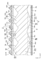
- the unit reflecting portion 41a reflects light at the inclined surface 41a1 disposed on the light incident surface 19b side in the first direction, thereby generating light whose incident angle with respect to the light emitting surface 19a does not exceed the critical angle. It is possible to promote emission from the light exit surface 19a.
- the unit reflecting portion 41a gradually increases in height dimension (dimension in the third direction) with increasing distance from the light incident surface 19b (LED 17) in the first direction, and the area (surface area) of the inclined surface 41a1 and the parallel surface 41a2 increases. It is arranged to gradually increase.
- the light emitted from the LED 17 and not entering the light incident surface 19b of the light guide plate 19 or the light leaking from the opposite end surface 19d and the side end surface 19e is the outer peripheral portion (particularly the end surface) of the liquid crystal panel 11 and the optical sheet 20. ) Can be shielded from direct incident light.
- the light shielding frame 21 three side portions (a pair of long side portions and a short side portion opposite to the LED substrate 18 side) that do not overlap with the LED 17 and the LED substrate 18 in plan view are chassis. 22 has a portion that rises from the bottom plate 22a and a portion that supports the frame 13 from the back side, but the short side portion that overlaps the LED 17 and the LED substrate 18 in a plan view is the end of the light guide plate 19.
- the LED board 18 (LED 17) are covered from the front side and bridged between a pair of long sides.
- the light shielding frame 21 is fixed to a chassis 22 described below by fixing means such as a screw member (not shown).
- the substrate accommodating portion 22a2 bulges to the back side.
- the substrate housing portion 22a2 has a substantially L-shaped cross-section, is bent from the end portion of the light guide plate support portion 22a1, and rises toward the back side, and a rising portion. It is composed of a receiving bottom 39 that is bent from the rising tip of 38 and protrudes toward the side opposite to the light guide plate support 22a1 side.
- the bent position of the rising portion 38 from the end of the light guide plate support portion 22a1 is located on the opposite side of the light incident surface 19b of the light guide plate 19 from the LED 17 side (near the center of the light guide plate support portion 22a1). .
- a long side side plate 22b is bent from the protruding tip of the housing bottom 39 so as to rise to the front side.
- the LED substrate 18 is attached to the side plate 22b on the short side continuous to the substrate housing portion 22a2, and the side plate 22b constitutes the substrate attachment portion 37.
- the board mounting portion 37 has a facing surface that faces the light incident surface 19b of the light guide plate 19, and the LED substrate 18 is mounted on the facing surface.
- the LED substrate 18 is fixed in such a manner that the plate surface opposite to the mounting surface 18a on which the LED 17 is mounted is in contact with the inner plate surface of the substrate mounting portion 37 via a substrate fixing member 25 such as a double-sided tape. ing.
- the attached LED board 18 has a slight gap between the LED board 18 and the inner plate surface of the housing bottom 39 that forms the board housing 22a2. Further, on the back plate surface of the bottom plate 22 a of the chassis 22, a liquid crystal panel drive circuit board (not shown) for controlling the drive of the liquid crystal panel 11, and an LED drive circuit board (not shown) for supplying drive power to the LEDs 17. A touch panel drive circuit board (not shown) for controlling the drive of the touch panel 14 is attached.
- the heat dissipating member 23 is made of a metal plate having excellent thermal conductivity such as an aluminum plate. As shown in FIG. 3, the heat dissipating member 23 is formed on one end of the short side of the chassis 22. It is set as the form extended along. As shown in FIG. 5, the heat dissipating member 23 has a substantially L-shaped cross section, and is parallel to the outer surface of the substrate housing portion 22a2 and in contact with the outer surface, and the substrate housing portion 22a2. It consists of the 2nd thermal radiation part 23b parallel to the outer surface of the continuous side plate 22b (board
- the first heat radiating portion 23a has an elongated flat plate shape extending along the Y-axis direction, and the plate surface facing the front side parallel to the X-axis direction and the Y-axis direction has a receiving bottom portion 39 in the substrate receiving portion 22a2. It is contact
- the first heat radiating portion 23a is screwed to the housing bottom 39 by a screw member SM, and has a screw insertion hole 23a1 through which the screw member SM is inserted.
- the accommodation bottom 39 is formed with a screw hole 28 into which the screw member SM is screwed.
- the second heat dissipating part 23b has an elongated flat plate shape extending along the Y-axis direction, and a plate surface facing inward in parallel to the Y-axis direction and the Z-axis direction is an outer plate in the board mounting part 37. They are arranged in a facing manner with a predetermined gap between them and the surface.
- the frame 13 constituting the liquid crystal display unit LDU will be described.
- the frame 13 is made of a metal material having excellent thermal conductivity such as aluminum.
- each outer peripheral portion (outer periphery) of the liquid crystal panel 11, the touch panel 14 and the cover panel 15 is used.
- it has a substantially rectangular frame shape (frame shape).
- press working or the like is employed as a method for manufacturing the frame 13, for example.
- the frame 13 presses the outer peripheral portion of the liquid crystal panel 11 from the front side, and the liquid crystal panel 11 and the optical sheet stacked with each other with the chassis 22 constituting the backlight device 12.
- the frame 13 receives the outer peripheral portions of the touch panel 14 and the cover panel 15 from the back side, and is arranged in a form interposed between the outer peripheral portions of the liquid crystal panel 11 and the touch panel 14.
- a predetermined gap is secured between the liquid crystal panel 11 and the touch panel 14.
- the touch panel 14 follows the cover panel 15 toward the liquid crystal panel 11. Even when it is deformed to bend, the bent touch panel 14 is less likely to interfere with the liquid crystal panel 11.
- the frame 13 includes a frame-shaped portion (frame base portion, frame-shaped portion) 13 a that follows the outer peripheral portions of the liquid crystal panel 11, the touch panel 14, and the cover panel 15, and the outer periphery of the frame-shaped portion 13 a. Attached to the chassis 22 and the heat radiating member 23 projecting from the frame-shaped part 13a toward the back side, and an annular part (cylindrical part) 13b that continues to the end and surrounds the touch panel 14, the cover panel 15 and the casing 16 from the outer peripheral side. And an attachment plate portion 13c.
- the frame-like portion 13a has a substantially plate shape having plate surfaces parallel to the plate surfaces of the liquid crystal panel 11, the touch panel 14, and the cover panel 15, and is formed in a rectangular frame shape when viewed from above.
- the frame portion 13a is relatively thicker at the outer peripheral portion 13a2 than at the inner peripheral portion 13a1, and a step (gap) GP is formed at the boundary between them.
- the inner peripheral portion 13a1 is interposed between the outer peripheral portion of the liquid crystal panel 11 and the outer peripheral portion of the touch panel 14, whereas the outer peripheral portion 13a2 receives the outer peripheral portion of the cover panel 15 from the back side. .
- the front plate surface of the frame-like portion 13a is almost entirely covered by the cover panel 15, the front plate surface is hardly exposed to the outside. Thereby, even if the temperature of the frame 13 is increased due to heat from the LED 17 or the like, it is difficult for the user of the liquid crystal display device 10 to directly contact the exposed portion of the frame 13, which is excellent in terms of safety.
- a buffer material 29 for fixing the outer peripheral portion of the liquid crystal panel 11 from the front side while buffering is fixed.
- the first fixing member 30 for fixing the outer peripheral portion of the touch panel 14 while buffering the outer peripheral portion of the touch panel 14 is fixed to the front plate surface of the inner peripheral portion 13a1.
- the first annular portion 34 is arranged so as to surround the outer peripheral end surfaces of the touch panel 14 and the cover panel 15 arranged on the front side with respect to the frame-shaped portion 13a over the entire circumference.
- the first annular portion 34 has an inner peripheral surface facing each outer peripheral end surface of the touch panel 14 and the cover panel 15, whereas the outer peripheral surface is exposed to the outside of the liquid crystal display device 10, and the liquid crystal display The external appearance of the side surface side of the device 10 is configured.
- the second annular portion 35 surrounds the front end portion (attachment portion 16c) of the casing 16 disposed on the back side with respect to the frame-shaped portion 13a from the outer peripheral side.
- the second annular portion 35 has an inner peripheral surface facing a mounting portion 16c of the casing 16 described later, whereas an outer peripheral surface is exposed to the outside of the liquid crystal display device 10 and the liquid crystal display device 10.
- the external appearance of the side surface is configured.
- a frame-side hooking claw portion 35a having a cross-sectional saddle shape is formed at the projecting tip portion of the second annular portion 35, and the casing 16 is locked to the frame-side locking claw portion 35a. The casing 16 can be held in the attached state.
- each of the mounting plate portions 13c disposed on the short side portion and the pair of long side portions on the opposite side to the LED substrate 18 side of the frame-like portion 13a has a plate surface facing the inner side of each of the chassis 22.
- Each of the side plates 22b is screwed with a screw member SM so as to be in contact with the outer plate surface.
- the mounting plate portions 13c are formed with screw insertion holes 13c1 through which the screw members SM are inserted, whereas the side plates 22b are formed with screw holes 36 into which the screw members SM are screwed. .
- Each screw member SM is attached to each attachment plate portion 13c in a form where a plurality of screw members SM are intermittently arranged along the extending direction.
- a terminal portion (not shown) connected to the end portion of the wiring drawn from the transparent electrode portion for the touch panel constituting the touch panel pattern is formed at one end portion on the short side of the touch panel 14.
- a flexible substrate (not shown)
- a potential is supplied from the touch panel drive circuit substrate to the transparent electrode portion for the touch panel forming the touch panel pattern.
- the touch panel 14 is fixed in a state where the inner plate surface in the outer peripheral portion thereof is opposed to the inner peripheral portion 13 a 1 in the frame-like portion 13 a of the frame 13 by the first fixing member 30 described above. Has been.
- the cover panel 15 assembled to the frame 13 will be described.
- the cover panel 15 is disposed so as to cover the touch panel 14 from the front side over the entire region, thereby protecting the touch panel 14 and the liquid crystal panel 11.
- the cover panel 15 covers the entire frame-like portion 13a of the frame 13 from the front side to the entire area, and configures the appearance of the front side of the liquid crystal display device 10.
- the cover panel 15 has a rectangular shape when seen in a plan view and is made of a plate-like base material made of glass that is substantially transparent and has excellent translucency, and preferably made of tempered glass.
- the member 31 is fixed to the outer peripheral portion 13a2 of the frame-like portion 13a of the frame 13 so as to face the outer peripheral portion 13a2.
- a central portion of the cover panel 15 that faces the touch panel 14 is laminated on the front side with respect to the touch panel 14 via an antireflection film AR.
- a light-blocking plate is provided on the inner (back side) plate surface (the plate surface facing the touch panel 14) in the outer peripheral portion including the above-described overhang portion 15 EP of the cover panel 15.
- a surface light shielding layer (light shielding layer, plate surface light shielding portion) 32 is formed.
- the plate surface light shielding layer 32 is made of a light shielding material such as a paint exhibiting black, for example, and the light shielding material is integrally provided on the plate surface by printing on the inner plate surface of the cover panel 15. It has been.
- printing means such as screen printing and ink jet printing can be employed.
- the casing 16 is made of a synthetic resin material or a metal material, and as shown in FIGS. 1, 3, and 4, has a substantially bowl shape that opens toward the front side. 13 covers the members such as the frame-shaped portion 13a, the mounting plate portion 13c, the chassis 22, and the heat dissipation member 23 from the back side, and configures the appearance of the back side of the liquid crystal display device 10.
- the casing 16 has a substantially flat bottom portion 16a, a curved portion 16b that rises from the outer peripheral edge of the bottom portion 16a toward the front side and has a curved cross section, and an attachment portion that rises almost straight from the outer peripheral edge of the curved portion 16b toward the front side.
- the attachment portion 16c is formed with a casing-side locking claw portion 16d having a saddle-shaped cross section, and the casing-side locking claw portion 16d is locked to the frame-side locking claw portion 35a of the frame 13.
- the casing 16 can be held in the attached state with respect to the frame 13.
- the backlight device 12 has a configuration for condensing the emitted light in the second direction (Y-axis direction), and the reason and configuration will be described below.
- the light propagating through the light guide plate 19 is reflected by the inclined surface 41 a 1 of the unit reflecting portion 41 a that constitutes the light output reflecting portion 41 and is raised.
- the incident angle with respect to the emission surface 19a is emitted with a critical angle or less, and the first direction (X-axis direction) is raised by the unit reflecting portion 41a in the front direction, that is, the light emission surface 19a.
- the light is focused toward the front side along the normal direction.
- the mold base is filled and the sheet base material 42b is directed to the opening end of the mold so that an uncured ultraviolet curable resin material is disposed in contact with the light-emitting side plate surface 42b2, and in this state the sheet base material 42b
- the ultraviolet curable resin material can be cured and the light output side unit prism 42a can be provided integrally with the sheet substrate 42b.
- the ultraviolet curable resin material forming the light output side unit prism 42a is, for example, an acrylic resin such as PMMA, and its refractive index is, for example, about 1.59.
- Each light output side unit prism 42a has a substantially isosceles triangular cross section, has a pair of inclined surfaces 42a1, and has an apex angle ⁇ v1 of approximately a right angle (90 °).
- the multiple light emitting side unit prisms 42a arranged in parallel along the second direction have the same apex angle ⁇ v1 and the width and height dimensions of the bottom surface 42a2, and are arranged between adjacent light emitting side unit prisms 42a. The intervals are almost constant and are arranged at equal intervals.
- the light utilization efficiency can be sufficiently increased, and the luminance related to the emitted light of the backlight device 12 can be further increased.
- the opposite plate surface side prism portion 44 is arranged on the opposite plate surface 19c side of the light guide plate 19, an anisotropic condensing portion is additionally arranged on the light output side with respect to the light guide plate 19. Compared to the case, the number of parts can be reduced, and the backlight device 12 can be made thinner.
- the light output reflection part of the light guide plate according to Comparative Example 3 has the same configuration as the light output reflection part 41 described before this paragraph.
- the opposite plate surface side prism portion 44 is not provided on the opposite plate surface of each light guide plate according to Comparative Examples 1 to 3
- the unit reflection portion provided to each light guide plate according to Comparative Examples 1 to 3 is provided. Are provided in a form extending continuously (without interruption in the middle) over the entire length of each light guide plate in the second direction.
- the unit reflection unit that forms the light output reflection unit depending on the presence or absence of the opposite plate side prism portion 44 is used.
- a comparative experiment 4 was conducted to obtain knowledge about what kind of change occurred in the shape reproducibility.
- the opposite plate surface side prism portion 44 is not provided on the opposite plate surface of the light guide plate according to Comparative Example 3.
- the unit reflection part provided in the light guide plate which concerns on the comparative example 3 is provided in the form extended continuously (without interruption on the way) over the full length of a light guide plate about the 2nd direction (Y-axis direction).
- the unit reflecting portion 41a is configured by a plurality of divided unit reflecting portions 41aS that are intermittently arranged at intervals in the second direction.
- the height dimension of the unit reflecting portion 41a can be relatively increased.
- the unit reflector 41a provided in the light guide plate 19 according to the first embodiment has a height dimension higher than that of the unit reflector provided in the light guide plate according to the comparative example 3. It is generally formed to be large.
- the light emitted from the light exit surface 19 a is further given an anisotropic condensing effect by the prism sheet 42 disposed on the light exit side with respect to the light guide plate 19. That is, the prism sheet 42 has a configuration in which a plurality of light output side unit prisms 42a extending along the first direction are arranged in a line along the second direction. The light condensing action is selectively given in the second direction, which is the arrangement direction of the light output side unit prisms 42a.
- the opposite plate surface side prism portion 44 is disposed on the opposite plate surface 19c side of the light guide plate 19, and the opposite plate surface side prism portion 44 extends in the first direction. Since the plurality of side unit prisms 44a are arranged in the second direction, the light transmitted through the light guide plate 19 and reaches the opposite plate surface 19c is arranged by the opposite plate side unit prisms 44a. A light condensing action is selectively given in the second direction which is the direction. Then, the light having such an anisotropic light condensing effect on the opposite plate surface 19c is raised toward the light emission surface 19a by the above-described light output reflection portion 41, and then light on the light emission surface 19a.
- the exit surface side prism portion 43 further selectively condenses the second direction. Therefore, it is possible to include more light that is emitted from the light exit surface 19a and directed toward the prism sheet 42 so as to be emitted without being retroreflected by the light exit side unit prism 42a. As a result, the light utilization efficiency can be sufficiently increased, and the luminance related to the emitted light of the backlight device 12 can be further increased. Moreover, since the opposite plate surface side prism portion 44 is arranged on the opposite plate surface 19c side of the light guide plate 19, an anisotropic condensing portion is additionally arranged on the light output side with respect to the light guide plate 19. Compared to the case, the number of parts can be reduced, and the backlight device 12 can be made thinner.
- the opposite plate surface side prism portion 44 is configured such that the opposite plate surface side unit condensing portion is formed as an opposite plate surface side unit prism 44a having a substantially triangular cross section.
- the opposite plate surface side unit condensing portion constituting the opposite plate surface side prism portion 44 is the opposite plate surface side unit prism 44a having a substantially triangular cross-section, and therefore the apex angle thereof. It is possible to adjust the intensity of the light condensing action applied to the light reaching the opposite plate surface 19c of the light guide plate 19 according to ⁇ v3.
- the prism sheet 42 is configured such that the light exit side unit condensing portion is a light exit side unit prism 42a having a substantially triangular cross section, and the light output side unit prism 42a has an apex angle ⁇ v1 of an opposite plate. It is smaller than the apex angle ⁇ v3 of the surface-side unit prism 44a.
- the light exit side unit condensing portion constituting the prism sheet 42 is the light exit side unit prism 42a having a substantially triangular cross section, and therefore the light guide plate 19 has a light emitting plate unit according to its apex angle ⁇ v1. It is possible to adjust the intensity of the light condensing action applied to the light emitted from the light exit surface 19a.
- the prism sheet 42 has a vertex angle ⁇ v1 of the light output side unit prism 42a smaller than the vertex angle ⁇ v3 of the opposite plate surface side unit prism 44a, so that more light is retroreflected compared to the opposite plate surface side prism portion 44.
- the emission angle range of the emitted light is more narrowly regulated and has a relatively strong condensing action.
- the light supplied to the prism sheet 42 is light-emitted on the light exit surface 19a after being provided with an anisotropic condensing action by the opposite plate surface side prism portion 44 on the opposite plate surface 19c of the light guide plate 19.
- the light exit surface side prism portion 43 is configured such that the light exit surface side unit condensing portion is a light exit surface side unit prism 43a having a substantially triangular cross section.
- the vertex angle ⁇ v2 of 43a is larger than the vertex angle ⁇ v1 of the light-emitting side unit prism 42a.
- the light emitting surface side unit prism 43a constituting the light emitting surface side prism portion 43 is the light emitting surface side unit prism 43a having a substantially triangular cross section, and therefore the apex angle ⁇ v2 thereof. Accordingly, it is possible to adjust the intensity of the light condensing action applied to the light reaching the light exit surface 19a of the light guide plate 19 according to the above.
- the prism sheet 42 has the apex angle ⁇ v1 of the light exit side unit prism 42a smaller than the apex angles ⁇ v2 and ⁇ v3 of the opposite plate surface side unit prism 44a and the light exit surface side unit prism 43a. Compared with the portion 44 and the light exit surface side prism portion 43, more light is retroreflected and the exit angle range of the exit light is more narrowly regulated, so that it has the strongest condensing action.
- the light supplied to the prism sheet 42 is light-emitted on the light exit surface 19a after being provided with an anisotropic condensing action by the opposite plate surface side prism portion 44 on the opposite plate surface 19c of the light guide plate 19.
- the ratio of retroreflected light at the light-emitting side unit prism 42a forming the prism sheet 42 is low and the light-emitting side unit prism 42a The light is emitted efficiently. Thereby, the utilization efficiency of light becomes higher and the luminance related to the emitted light of the backlight device 12 can be further increased.
- the light emitting surface side prism portion 43 and the opposite plate surface side prism portion 44 are provided integrally with the light guide plate 19. In this case, the number of parts can be reduced compared to the case where the light emitting surface side prism portion and the opposite plate surface side prism portion are provided as separate components from the light guide plate 19, so that the cost can be reduced. It is suitable.
- the liquid crystal display device (display device) 10 includes the above-described backlight device 12 and a liquid crystal panel (display panel) 11 that performs display using light from the backlight device 12.
- the liquid crystal display device 10 having such a configuration, since the front luminance related to the light emitted from the backlight device 12 is high and luminance unevenness hardly occurs, display with excellent display quality can be realized. it can.
- the display panel is a liquid crystal panel 11 in which liquid crystal is sealed between a pair of substrates 11a and 11b.
- a display device can be applied to the liquid crystal display device 10 for various uses, for example, a display of a smartphone or a tablet personal computer.
- a light emitting surface 119a of a light guide plate 119 is provided with a flat portion 45 in addition to the light emitting surface side prism portion 143.
- movement, and effect as above-mentioned Embodiment 1 is abbreviate
- the light exit surface 119 a of the light guide plate 119 has a first direction (X-axis direction) and a second direction (in addition to the light exit surface side prism portion 143).
- a flat portion 45 having a flat shape is provided along the (Y-axis direction).
- the light emitting surface 119a of the light guide plate 119 has a plurality of light emitting surface side unit prisms 143a arranged along the second direction at predetermined intervals, and light adjacent to the second direction.
- a flat portion 45 is arranged so as to be interposed between the exit surface side unit prisms 143a.
- the light emitting surface side unit prisms 143a and the flat portions 45 are arranged in an alternating and repeated manner along the second direction.
- the width dimension of the flat portion 45 (dimension in the second direction) is smaller than the width dimension of the light emitting surface side unit prism 143a.
- the flat part 45 is provided in the form extended over the full length of the light-guide plate 119 about a 1st direction.
- light exit surface side unit prisms 143a are respectively disposed at both ends of the light guide plate 119 in the second direction.
- the number of the light exit surface side unit prisms 143a is “n”
- the light guide plate 119 is flat.
- the number of installed units 45 is “n ⁇ 1”. That is, the number of installed light exit surface side unit prisms 143a is larger than the number of installed flat portions 45.
- Light that enters the light guide plate 119 from the LED propagates through the light guide plate 119 and reaches the light exit surface 119a.
- the light reaching the light exit surface 119a is emitted while being provided with an anisotropic condensing function by the light exit surface side unit prism 143a, and is totally reflected by the light exit surface side unit prism 143a and opposite to the opposite plate.
- What is returned to the surface 119c side and what is totally reflected by the flat portion 45 and returned to the opposite plate surface 119c side are included at least.
- the light returned to the opposite plate surface 119c side by the flat portion 45 is about the second direction as compared with the light totally reflected by the light emitting surface side unit prism 143a and returned to the opposite plate surface 119c side.
- the light propagates through the light guide plate 119 while spreading over a wider range. Accordingly, the light propagating through the light guide plate 119 is appropriately diffused in the second direction and then emitted while being provided with an anisotropic condensing function by the light exit surface side unit prism 143a. Luminance unevenness hardly occurs in the incident light.
- Comparative Experiment 5 was performed in order to obtain knowledge regarding whether or not luminance unevenness occurs in the light emitted from the light exit surface of the light guide plate according to the presence or absence of the flat portion 45 and the ratio of the flat portion 45.
- the same light guide plate (light guide plate not provided with a flat portion) as that of the first embodiment described in the comparative experiment 1 of the first embodiment is used as the comparative example 4, and the light emitting surface 119a has an area ratio.
- a light guide plate 119 provided with a flat portion 45 of 20% is referred to as Example 9
- a light guide plate 119 provided with a flat portion 45 of which the area ratio is 40% on the light emitting surface 119a is referred to as Example 10. .
- the light exit surface 119a of the light guide plate 119 is disposed between the light exit surface side unit prisms 143a adjacent to each other in the second direction along the first direction and the second direction.
- a flat flat portion 45 is provided. In this way, light that propagates through the light guide plate 119 and reaches the light exit surface 119a is totally reflected by the flat portion 45 and returned to the opposite plate surface 119c side.
- the light returned to the opposite plate surface 119c side by the flat portion 45 is spreading more in the second direction than the light totally reflected by the light emitting surface side unit prism 143a and returned to the opposite plate surface 119c side.
- the light propagates through the light guide plate 119. Therefore, it is difficult for luminance unevenness to occur in the light emitted from the backlight device.
- the light emitting surface side prism portion 243 has a first light emitting surface side unit prism 243aA having a relatively small height dimension and a second element having a relatively large height dimension. And a light emitting surface side unit prism 243aB.
- the second light exit surface side unit prism 243aB is the same as the light exit surface side unit prism 43a described in the first embodiment in the height dimension, the apex angle, and the like.
- the first light exit surface side unit prism 243aA has a cross-sectional shape cut along the second direction (Y-axis direction) as a substantially isosceles triangle, and the apex angle thereof is the apex angle of the second light exit surface side unit prism 243aB. Is the same. That is, the first light exit surface side unit prism 243aA has a cross-sectional shape similar to that of the second light exit surface side unit prism 243aB.
- the second light exit surface side unit prism 243aB has a bottom surface whose width and height are larger than those of the first light exit surface side unit prism 243aA.
- the width and height of the bottom surface of the first light exit surface side unit prism 243aA are each about twice as large. Accordingly, the second light exit surface side unit prism 243aB is arranged at a position where the top portion 243aB1 is relatively higher than the top portion 243aA1 of the first light exit surface side unit prism 243aA (position close to the prism sheet 242).
- the prism sheet 242 is arranged in contact with the plate surface on the back side (light guide plate 219 side).
- the first light exit surface side unit prism 243aA is arranged at a position where the top portion 243aA1 is relatively lower than the top portion 243aB1 of the second light exit surface side unit prism 243aB (position far from the prism sheet 242).
- a gap C is provided between the prism sheet 242 and the back plate. That is, the first light exit surface side unit prism 243aA is maintained in a non-contact state with respect to the plate surface on the back side of the prism sheet 242.
- the contact area between the light guide plate 219 and the prism sheet 242 is reduced as compared with the first embodiment, and an air layer is present in the gap C generated between the light guide plate 219 and the prism sheet 242.
- the second light emitting surface side unit prisms 243aB are intermittently arranged in the second direction, and specifically, three first light emitting surface side units between the adjacent second light emitting surface side unit prisms 243aB.
- the prism 243aA is disposed so as to be sandwiched.
- the second light emitting surface side unit prisms 243aB are arranged in an intermittently arranged manner with a constant period (each of the three first light emitting surface side unit prisms 243aA). A gap C between the prism 243aA and the prism sheet 242 is stably maintained.
- Example 5 a light guide plate having light emitting surface side unit prisms whose height dimensions are all the same, and a light guide plate 219 having two kinds of large and small light emitting surface side unit prisms 243aA and 243aB having different height dimensions.
- the comparative experiment 6 shown below was performed using each.
- the same light guide plate as the example 1 described in the comparative experiment 1 of the above-described embodiment 1 (light guide plate having light emitting surface side unit prisms all having the same height dimension) is compared.
- Example 5 a light guide plate 219 having two types of light emitting surface side unit prisms 243aA and 243aB having different height dimensions is used as Example 11.
- Each light guide plate 219 according to Example 11 has the same structure as the light guide plate 219 described before this paragraph.
- the light guide plate 219 according to Example 11 has the same structure as the light guide plate according to Comparative Example 5 except that the light guide plate 219 has two types of light emitting surface side unit prisms 243aA and 243aB having different height dimensions.
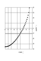
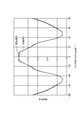
- FIG. 22 shows the result of measuring the luminance distribution regarding the emitted light obtained by transmitting the emitted light from each light guide plate according to Comparative Example 5 and Example 11 through the prism sheet 242.
- the vertical axis represents the relative luminance (no unit) of the light emitted from the prism sheet 242, and the horizontal axis represents the angle with respect to the front direction in the second direction (the unit is “°”).
- the relative luminance on the vertical axis in FIG. 22 is a relative value based on the luminance value in the front direction (angle 0 °) when the light guide plate 219 according to Example 11 is used as a reference (1.0).
- the graph indicated by a solid line represents Example 11
- the graph indicated by a broken line represents Comparative Example 5.
- the plurality of light exit surface side unit prisms 243a forming the light exit surface side prism portion 243 includes the first light exit surface side unit prism in which the position of the top portion 243aA1 is relatively low.
- (First light exit surface side unit condensing portion) 243aA and a second light exit surface side unit prism (second light exit surface side unit condensing portion) 243aB in which the position of the top portion 243aB1 is relatively high are included.
- a gap C is provided between the first light exit surface side unit prism 243aA and the prism sheet 242.
- the light emission surface side prism portion is formed by providing the gap C between the first light emission surface side unit prism 243a and the prism sheet 242 included in the plurality of light emission surface side unit prisms 243a. It is difficult for the prism sheet 242 to be in close contact with the H.243. Thereby, generation
- ⁇ Embodiment 4> A fourth embodiment of the present invention will be described with reference to FIG. 23 or FIG.
- a light emitting surface side lenticular lens portion 46 is provided in place of the light emitting surface side prism portion 43 described in the first embodiment.
- movement, and effect as above-mentioned Embodiment 1 is abbreviate
- the light exit surface 319a of the light guide plate 319 can selectively condense the emitted light in the second direction (Y-axis direction).
- a surface side lenticular lens part (light exit surface side anisotropic condensing part) 46 is provided.
- the light exit surface side lenticular lens portion 46 is arranged in a form in which a plurality of cylindrical lenses (light exit surface side unit condensing portions) 46a extending in the first direction (X-axis direction) are arranged in the second direction. It is supposed to be.
- the light exit surface side lenticular lens portion 46 is provided integrally with the light guide plate 319.
- the light guide plate 319 is manufactured by injection molding, and the light exit surface side lenticular lens portion 46 is transferred in advance to the molding surface of the molding die.
- a transfer shape may be formed.
- the cylindrical lens 46a has a substantially semi-cylindrical shape whose axial direction coincides with the first direction, and the surface facing the front side has an arc shape.
- a cross-sectional shape cut along a parallel direction (second direction) orthogonal to the extending direction (first direction) has a substantially semicircular shape (saddle shape).
- the second direction is the light collection direction of the cylindrical lens 46a.
- the light passing through the focal point of the cylindrical lens 46a can be emitted as light substantially parallel to the front direction by being refracted by the arcuate outer surface.
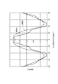
- the light collection effect which selectively raises the light which goes to a 2nd direction among the emitted light from the light-projection surface 319a, and makes the advancing direction turn to a front direction (approaching) is acquired.
- the cylindrical lens 46a has a tangent angle ⁇ t of, for example, about 70 ° when an angle ⁇ t formed by the tangent Ta at the base end portion 46a1 of the arcuate surface with respect to the second direction is a “tangential angle”. Is done.
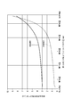
- a comparative experiment 7 was performed to obtain knowledge on how the luminance unevenness suppressing effect changes depending on the shape of the cylindrical lens 46a.
- the angle ⁇ t formed by the tangent Ta at the base end portion 46a1 of the arcuate surface of the cylindrical lens 46a with respect to the second direction is defined as the “tangential angle”, and the tangential angle Light guide plates 319 each having a light exit surface side lenticular lens portion 46 formed of a cylindrical lens 46a with ⁇ t of 20 °, 30 °, 40 °, 60 °, and 70 ° were prepared.
- each light guide plate 319 having a tangent angle ⁇ t of 20 °, 30 °, 40 °, 60 °, and 70 °, and the light exit surface 319a of each light guide plate 319 is incident.
- a photograph was taken from the light emitting surface 319a side with light emitted from the light source, and the presence or absence of luminance unevenness was determined based on the photograph.
- the experimental results are shown in the table of FIG. In FIG.
- the cylindrical lens 46a preferably has a tangent angle ⁇ t of 40 ° or more.
- the light exit surface side lenticular lens (light exit surface side anisotropic condensing part) 46 is a light exit surface side unit condensing part, and has a cylindrical surface whose surface is arcuate. It is set as the lens 46a. In this case, it is assumed that luminance unevenness is less likely to occur in the emitted light of the backlight device as compared with a case where the light exit surface side unit condensing unit is a prism having a triangular cross-sectional shape.
- a fifth embodiment of the present invention will be described with reference to FIG.
- the unit shape of the unit reflection portion 441a forming the light output reflection portion 441 is changed from that in the first embodiment.
- movement, and effect as above-mentioned Embodiment 1 is abbreviate
- the unit reflection portion 441a that forms the light output reflection portion 441 according to the present embodiment has a cross-sectional shape of a non-right triangle as shown in FIG. Accordingly, the unit reflecting portion 441a has a pair of inclined surfaces 441a1A and 441a1B that are inclined with respect to the third direction (Z-axis direction) and the first direction (X-axis direction).
- the first inclined surface 441a1A disposed on the light incident surface side (not shown) in the first direction has an angle formed with respect to the first direction on the opposite end surface side not shown in the first direction.
- the second inclined surface 441a1B disposed on the right side shown in FIG.
- the unit reflecting portion 441a mainly reflects light at the first inclined surface 441a1A, thereby generating light whose incident angle with respect to the light emitting surface 419a does not exceed the critical angle. It is possible to prompt emission from the emission surface 419a.
- the unit reflecting portion 441a gradually increases in height (dimension in the third direction) with increasing distance from a light incident surface (not shown) in the first direction, and the areas (surface areas) of the inclined surfaces 441a1A and 441a1B gradually increase. It is arranged to be larger.
- the prism sheet 542 has a configuration in which the light output side unit prism 542a and the sheet base material 542b are integrally formed of the same material.
- the prism sheet 542 is made of, for example, polycarbonate (PC) and has a refractive index of about 1.59. Even with such a configuration, the same operations and effects as those described in the first embodiment can be obtained.
- Embodiment 7 A seventh embodiment of the present invention will be described with reference to FIG. In this Embodiment 7, what changed the shape of the 2nd light-projection surface side unit prism 643aB from Embodiment 3 mentioned above is shown. In addition, the overlapping description about the same structure, effect
- the second light emitting surface side unit prism 643aB forming the light emitting surface side prism portion 643 according to the present embodiment has a top portion 643aB1 that is rounded in an arc shape and has a curved surface. Yes.
- the top portion 643aB1 of the second light emitting surface side unit prism 643aB is in direct contact with the plate surface on the back side of the prism sheet 642, but has a rounded shape.
- the top 643aB1 of the surface-side unit prism 643aB is rubbed and the prism sheet 642 is rubbed and scratched, or conversely, the prism sheet 642 interferes with the top 643aB1 of the second light emitting surface-side unit prism 643aB, so that the top 643aB1 is deformed. It is difficult for the situation to occur. Thereby, the optical performance of the light guide plate 619 and the prism sheet 642 is unlikely to deteriorate.
- the light emitting surface 719a of the light guide plate 719 has a flat portion 745 and a cylindrical lens 746a forming the light emitting surface side lenticular lens portion 746 in the second direction (Y (Axial direction) are provided side by side.
- the flat portions 745 and the cylindrical lenses 746a are arranged in an alternating and repeated manner along the second direction. According to such a configuration, it is possible to obtain both the luminance unevenness suppressing effect by the flat portion 745 and the luminance unevenness suppressing effect by the cylindrical lens 746a, so that the luminance unevenness is less likely to occur in the light emitted from the light guide plate 719. It is said.
- a ninth embodiment of the present invention will be described with reference to FIG.
- a light emitting surface side lenticular lens portion 846 having the same configuration as that of the above described fourth embodiment is provided instead of the light emitting surface side prism portion 243 described in the third embodiment.
- action, and effect as above-mentioned Embodiment 3, 4 is abbreviate
- the light emitting surface 819a of the light guide plate 819 has a first cylindrical lens 846aA having a relatively small height dimension and a second cylindrical lens having a relatively large height dimension. 846aB and a light exit surface side lenticular lens portion 846 is provided.
- the first cylindrical lens 846aA has the same height and tangent angle as the cylindrical lens 46a described in the fourth embodiment.
- the second cylindrical lens 846aB has a semicircular cross section cut along the second direction (Y-axis direction), and the tangent angle thereof is the same as the tangential angle of the first cylindrical lens 846aA.
- the second cylindrical lens 846aB has a cross-sectional shape similar to that of the first cylindrical lens 846aA. According to such a configuration, it is possible to prevent the light guide plate 819 from sticking to the prism sheet 842, and it is difficult for luminance unevenness to occur in the light emitted from the light guide plate 819.
- ⁇ Other embodiments> The present invention is not limited to the embodiments described with reference to the above description and drawings. For example, the following embodiments are also included in the technical scope of the present invention.
- a plurality of unit reflection portions forming the light output reflection portion are arranged at equal intervals in the first direction (equal pitch arrangement).
- the present invention includes a configuration in which the reflecting portions are arranged at an unequal pitch in the first direction. In that case, it is preferable in order to suppress luminance unevenness to set the arrangement interval between the adjacent unit reflection portions so as to gradually become narrower from the light incident surface side to the opposite end surface side of the light guide plate.
- the height dimensions of the plurality of unit reflection portions arranged along the first direction are made constant. Is also possible.
- the height dimension of the unit reflecting portion that forms the light output reflecting portion is smaller than the height dimension of the opposite plate surface side unit prism that forms the opposite plate surface side prism section.
- the height dimension of the unit reflecting portion can be set to be approximately the same as the height dimension of the opposite plate surface side unit prism.
- the specific cross-sectional shape of the unit reflecting portion that forms the light output reflecting portion can be changed as appropriate.
- the cross-sectional shape of the unit reflection part can be an isosceles triangle.
- each specific angle in each vertex of the unit reflection part whose cross-sectional shape is a triangle can be changed as appropriate.
- specific values such as the height dimension, the width dimension, and the arrangement interval in the first direction of the unit reflecting section forming the light output reflecting section can be appropriately changed.
- the cross-sectional shape of the opposite plate-side unit prism forming the opposite plate-side prism portion is an isosceles triangle, but the cross-sectional shape of the opposite plate-side unit prism is For example, it is possible to use an unequal triangle or a right triangle in which all the sides have different lengths.
- the light emitting surface side unit prism forming the light emitting surface side prism portion is shown to have an isosceles triangular cross section, but the light emitting surface side unit prism has a cross sectional shape of For example, it is possible to use an unequal triangle or a right triangle in which all the sides have different lengths.
- specific values such as the apex angle, height dimension, width dimension, and arrangement interval in the second direction of the opposite-plate-side unit prism that forms the opposite-plate-side prism portion Can be appropriately changed.
- specific values such as an apex angle, a height dimension, a width dimension, and an arrangement interval in the second direction in the light emitting surface side unit prism forming the light emitting surface side prism portion can be changed as appropriate.
- specific values such as an apex angle, a height dimension, a width dimension, and an arrangement interval in the second direction in the light-emitting side unit prism forming the prism sheet can be appropriately changed.
- the opposite plate surface side prism portion provided on the opposite plate surface of the light guide plate is composed of the opposite plate surface side unit prism having a triangular cross-sectional shape.
- an opposite plate surface side lenticular lens portion comprising a plurality of cylindrical lenses having a substantially semi-cylindrical shape whose axial direction coincides with the first direction (X-axis direction) is provided.
- the opposite plate surface side anisotropic condensing part may be provided on the opposite plate surface of the light guide plate.
- the prism sheet is provided with the light-emitting side unit prism having a triangular cross-sectional shape.
- the axial direction is the first.
- a plurality of cylindrical lenses having a substantially semi-cylindrical shape that coincides with one direction (X-axis direction) may be provided on the prism sheet.
- the light emitting surface side prism portion or the light emitting surface side lenticular lens portion is integrally provided on the light emitting surface of the light guide plate.
- the light exit surface side lenticular lens portion is provided as a separate component from the light guide plate, and the light exit surface side prism portion or the light exit surface side lenticular lens portion that is a separate component overlaps the light exit surface of the light guide plate. It is also possible to adopt a configuration of arranging in a form.
- the refractive index of the material forming the light emitting surface side prism portion or the light emitting surface side lenticular lens portion as a separate part is the same as the refractive index of the material forming the light guide plate. Furthermore, it is preferable that the material forming the light emitting surface side prism portion or the light emitting surface side lenticular lens portion as a separate part is the same as the material forming the light guide plate.
- the flat portion and the light emitting surface side unit prisms are arranged alternately and repeatedly in the second direction.
- the two flat shapes in the second direction are shown. It is also possible to dispose a plurality of light emitting surface side unit prisms between the units.
- the specific value of the area ratio of the flat portion on the light exit surface of the light guide plate can be changed as appropriate.
- the specific value of the area ratio of the flat portion can be changed as appropriate.
- the flat portion is provided on the light exit surface of the light guide plate, but it is also possible to provide the flat portion on the opposite plate surface of the light guide plate.
- the flat plate portion may be disposed between the plurality of opposite plate surface side unit prisms that form the opposite plate surface side prism portion and are arranged along the second direction.
- the first light exit surface side unit prism and the second light exit surface side unit prism have similar cross-sectional shapes, but the first light exit surface side is shown.
- the unit prism and the second light exit surface side unit prism whose cross-sectional shapes are not similar are also included in the present invention.
- the apex angle of the first light exit surface side unit prism may be different from the apex angle of the second light exit surface side unit prism.
- the tangential angle of the first cylindrical lens and the tangential angle of the second cylindrical lens may be set differently.
- the light emitting surface side prism portion is composed of two types of light emitting surface side unit prisms having different height dimensions.
- the light emitting surface side prism portion has three or more types having different height dimensions. It is also possible to configure the light exit surface side prism portion by the light exit surface side unit prism.
- the light exit surface side lenticular lens portion can also be configured by three or more types of cylindrical lenses having different height dimensions.
- the light exit surface side prism portion is configured by two types of light exit surface side unit prisms having different height dimensions. What comprises two or more types of opposite plate side unit prisms having different height dimensions is also included in the present invention. Similarly, two or more types of light-emitting side unit prisms having different height dimensions may be provided on the prism sheet.
- the specific tangent angle value of the cylindrical lens can be changed as appropriate.
- the specific tangent angle value of the cylindrical lens can be changed as appropriate.
- the optical sheet is configured to include only one prism sheet.
- another type of optical sheet for example, a diffusion sheet or a reflective polarizing sheet
- a diffusion sheet or a reflective polarizing sheet is added.
- one LED substrate is disposed along the light incident surface of the light guide plate.
- two or more LED substrates are disposed along the light incident surface of the light guide plate. Those arranged in a line are also included in the present invention.
- the one side surface on the short side of the light guide plate is used as the light incident surface, and the LED substrate is arranged opposite to the light incident surface.
- the present invention includes one in which one side surface on the side is a light incident surface, and the LED substrate is arranged opposite to the light incident surface.
- the extending direction of the light exit side unit prism, the light exit surface side unit prism, and the opposite plate surface side unit prism is matched with the short side direction of the light guide plate, the light exit side unit prism, the light exit surface side unit prism,
- the width direction (alignment direction) of the opposite plate surface side unit prisms may be made to coincide with the long side direction of the light guide plate.
- the present invention includes a configuration in which a pair of end surfaces on the long side of the light guide plate are respectively light incident surfaces, and a pair of LED substrates are arranged opposite to each light incident surface.
- the light guide plate is rectangular, but the light guide plate may be square. Further, the light guide plate does not have to be a complete square, and may have a configuration in which a part of the outer peripheral end is cut away.
- the projected capacitive type is exemplified as the touch panel pattern of the touch panel, but other than that, the touch panel of the surface capacitive type, the resistive film type, the electromagnetic induction type, etc.
- the present invention can also be applied to those employing patterns.
- an image displayed on the display surface of the liquid crystal panel is separated by parallax, so that a stereoscopic image (3D image, 3D image) is displayed to the observer.
- a parallax barrier panel switch liquid crystal panel
- the above-described parallax barrier panel and touch panel can be used in combination.
- the screen size of the liquid crystal panel used in the liquid crystal display device is set to about 20 inches is exemplified, but the specific screen size of the liquid crystal panel can be appropriately changed to other than 20 inches. It is. In particular, when the screen size is about several inches, it is preferably used for an electronic device such as a smartphone.
- the color part of the color filter included in the liquid crystal panel is exemplified as three colors of R, G, and B.
- the color part may be four or more colors.
- an LED is used as a light source, but other light sources such as an organic EL can also be used.
- the frame is made of metal, but the frame can be made of synthetic resin.
- the cover panel using tempered glass is shown, but it is of course possible to use a normal glass material (non-tempered glass) or a synthetic resin material that is not tempered glass.
- a TFT is used as a switching element of a liquid crystal display device.
- the present invention can also be applied to a liquid crystal display device using a switching element other than TFT (for example, a thin film diode (TFD)).
- a switching element other than TFT for example, a thin film diode (TFD)
- the present invention can also be applied to a liquid crystal display device for monochrome display.
- SYMBOLS 10 Liquid crystal display device (display device), 11 ... Liquid crystal panel (display panel), 11a, 11b ... Substrate, 12 ... Backlight device (illumination device), 17 ... LED (light source) ), 19, 119, 219, 319, 419, 619, 719, 819 ... light guide plate, 19a, 119a, 319a, 419a, 719a, 819a ... light exit surface, 19b ... light entrance surface, 19c , 119c ... opposite plate surface (plate surface), 19e ... side end surface (a pair of end surfaces not including the light incident surface), 41, 441 ... light output reflection part, 41a, 441a ...
- unit reflection part 41aS ... divided unit reflector, 42, 242, 542, 642 ... prism sheet (light-emitting side anisotropic light collecting part), 42a, 542a ... light-emitting side unit prism (light-emitting side unit light collecting part) ), 43, 143, 243, 643 ... Light exit surface side prism portion (light exit surface side anisotropic condensing) ), 43a, 143a ... light exit surface side unit prism (light exit surface side unit condensing portion), 44 ... opposite plate surface side prism portion (opposite plate surface side anisotropic condensing portion), 44a. ..
- Opposite plate-side unit prism opposite plate-side unit condensing unit
- 44a2 Opposite plate-side unit prism
- 44a2 Opposite plate-side unit condensing unit
- 44a2 Opposite plate-side unit condensing unit
- 44a2 Opposite plate-side unit condensing unit
- 44a2 Opposite plate-side unit condensing unit
- 44a2 Opposite plate-side unit condensing unit
- 44a2 Opposite plate-side unit condensing unit
- 44a2 Opposite plate-side unit condensing unit
- 44a2 Opposite plate-side unit condensing unit
- 44a2 Opposite plate-side unit condensing unit
- 44a2 Opposite plate-side unit condensing unit
- 44a2 Opposite plate-side unit condensing unit
- 44a2 Opposite plate-side unit condensing unit
Abstract
L'invention concerne un dispositif (12) de rétro-éclairage, comportant: une DEL (17); une plaque guide (19) de lumière présentant une surface (19b) d'entrée de lumière, une surface (19a) de sortie de lumière et un surface (19c) de plaque opposée; une nappe (42) de prismes disposée sur le côté de sortie de lumière de la plaque guide (19) de lumière et obtenue en disposant une pluralité de prismes (42a) d'unité de côté sortie de lumière en une rangée suivant une deuxième direction; une unité (43) de prismes côté surface de sortie de lumière disposée du côté de la surface (19a) de sortie de lumière de la plaque guide (19) de lumière et obtenue en disposant une pluralité de prismes (43a) d'unité de côté surface de sortie de lumière en une rangée suivant la deuxième direction; une partie réfléchissante (41) de sortie de lumière disposée du côté de la surface (19c) de plaque opposée de la plaque guide (19) de lumière et obtenue en disposant une pluralité de parties unitaires (41a) de réflexion à intervalles en une rangée suivant une première direction; et une unité (44) de prismes côté surface de plaque opposée disposée du côté de la surface (19c) de plaque opposée de la plaque guide (19) de lumière et obtenue en disposant une pluralité de prismes (44a) de côté surface de plaque opposée en une rangée suivant la deuxième direction.
Priority Applications (1)
| Application Number | Priority Date | Filing Date | Title |
|---|---|---|---|
| US15/105,537 US10317610B2 (en) | 2013-12-18 | 2014-12-12 | Illumination device and display device |
Applications Claiming Priority (2)
| Application Number | Priority Date | Filing Date | Title |
|---|---|---|---|
| JP2013261098 | 2013-12-18 | ||
| JP2013-261098 | 2013-12-18 |
Publications (1)
| Publication Number | Publication Date |
|---|---|
| WO2015093396A1 true WO2015093396A1 (fr) | 2015-06-25 |
Family
ID=53402743
Family Applications (1)
| Application Number | Title | Priority Date | Filing Date |
|---|---|---|---|
| PCT/JP2014/082932 WO2015093396A1 (fr) | 2013-12-18 | 2014-12-12 | Dispositif d'éclairage et dispositif d'affichage |
Country Status (2)
| Country | Link |
|---|---|
| US (1) | US10317610B2 (fr) |
| WO (1) | WO2015093396A1 (fr) |
Cited By (1)
| Publication number | Priority date | Publication date | Assignee | Title |
|---|---|---|---|---|
| WO2018006418A1 (fr) * | 2016-07-08 | 2018-01-11 | 华为技术有限公司 | Film appliqué sur un écran d'affichage, écran d'affichage et terminal |
Families Citing this family (9)
| Publication number | Priority date | Publication date | Assignee | Title |
|---|---|---|---|---|
| CN107526200B (zh) | 2013-03-08 | 2021-05-07 | Lg电子株式会社 | 显示装置 |
| US9921360B2 (en) | 2013-12-24 | 2018-03-20 | Sharp Kabushiki Kaisha | Illumination device and display device |
| CN106019666B (zh) * | 2015-03-31 | 2023-03-28 | 天马微电子股份有限公司 | 显示装置及显示装置的制造方法 |
| KR101733522B1 (ko) * | 2015-05-28 | 2017-05-10 | 엘지디스플레이 주식회사 | 표시모듈 및 이를 이용한 액정표시장치 |
| JP7203366B2 (ja) * | 2017-03-16 | 2023-01-13 | パナソニックIpマネジメント株式会社 | 表示装置 |
| US10225458B2 (en) * | 2017-07-07 | 2019-03-05 | HKC Corporation Limited | Display panel and display apparatus using the same |
| JP2020119678A (ja) * | 2019-01-21 | 2020-08-06 | シャープ株式会社 | 照明装置及び表示装置 |
| CN211979374U (zh) * | 2020-04-17 | 2020-11-20 | 京东方科技集团股份有限公司 | 调光组件、背光模组及液晶显示装置 |
| TWI777690B (zh) * | 2021-07-26 | 2022-09-11 | 群光電能科技股份有限公司 | 觸控板模組 |
Citations (2)
| Publication number | Priority date | Publication date | Assignee | Title |
|---|---|---|---|---|
| JP2011014442A (ja) * | 2009-07-03 | 2011-01-20 | Mitsubishi Rayon Co Ltd | 面光源装置及びそれに用いる導光体 |
| JP2012104390A (ja) * | 2010-11-10 | 2012-05-31 | Stanley Electric Co Ltd | 面光源装置 |
Family Cites Families (9)
| Publication number | Priority date | Publication date | Assignee | Title |
|---|---|---|---|---|
| JPH0961631A (ja) | 1995-08-22 | 1997-03-07 | Nippon Chemitec Kk | 導光板と該導光板を使用した面型照明体 |
| KR100830340B1 (ko) * | 2006-07-04 | 2008-05-16 | 삼성에스디아이 주식회사 | 백라이트 유니트의 도광판 및 이를 구비한 백라이트 유니트 |
| KR101440498B1 (ko) | 2007-11-12 | 2014-09-18 | 삼성디스플레이 주식회사 | 도광판 및 이를 갖는 표시장치 |
| KR101258902B1 (ko) * | 2008-12-31 | 2013-05-07 | 엘지디스플레이 주식회사 | 프리즘시트, 이를 구비한 백라이트장치 및 액정표시소자 |
| MY156117A (en) | 2010-10-15 | 2016-01-15 | Sharp Kk | Backlight unit |
| JP2012113890A (ja) | 2010-11-22 | 2012-06-14 | Mitsubishi Rayon Co Ltd | 導光体、面光源装置及び画像表示装置 |
| JP5927536B2 (ja) | 2011-07-05 | 2016-06-01 | パナソニックIpマネジメント株式会社 | 導光板および面光源装置 |
| WO2013005559A1 (fr) | 2011-07-06 | 2013-01-10 | シャープ株式会社 | Dispositif d'éclairage et dispositif d'affichage |
| US9921360B2 (en) | 2013-12-24 | 2018-03-20 | Sharp Kabushiki Kaisha | Illumination device and display device |
-
2014
- 2014-12-12 WO PCT/JP2014/082932 patent/WO2015093396A1/fr active Application Filing
- 2014-12-12 US US15/105,537 patent/US10317610B2/en active Active
Patent Citations (2)
| Publication number | Priority date | Publication date | Assignee | Title |
|---|---|---|---|---|
| JP2011014442A (ja) * | 2009-07-03 | 2011-01-20 | Mitsubishi Rayon Co Ltd | 面光源装置及びそれに用いる導光体 |
| JP2012104390A (ja) * | 2010-11-10 | 2012-05-31 | Stanley Electric Co Ltd | 面光源装置 |
Cited By (2)
| Publication number | Priority date | Publication date | Assignee | Title |
|---|---|---|---|---|
| WO2018006418A1 (fr) * | 2016-07-08 | 2018-01-11 | 华为技术有限公司 | Film appliqué sur un écran d'affichage, écran d'affichage et terminal |
| US10823896B2 (en) | 2016-07-08 | 2020-11-03 | Huawei Technologies Co., Ltd. | Film having parallel protrusions applied to display, display, and terminal |
Also Published As
| Publication number | Publication date |
|---|---|
| US20160313496A1 (en) | 2016-10-27 |
| US10317610B2 (en) | 2019-06-11 |
Similar Documents
| Publication | Publication Date | Title |
|---|---|---|
| JP6349398B2 (ja) | 照明装置及び表示装置 | |
| JP6403756B2 (ja) | 照明装置及び表示装置 | |
| WO2016093137A1 (fr) | Dispositif d'éclairage et dispositif d'affichage | |
| WO2016017487A1 (fr) | Dispositif d'éclairage, et dispositif d'affichage | |
| WO2014157482A1 (fr) | Dispositif d'éclairage et dispositif d'affichage | |
| WO2015093396A1 (fr) | Dispositif d'éclairage et dispositif d'affichage | |
| WO2014157461A1 (fr) | Dispositif d'éclairage et dispositif d'affichage | |
| WO2014010523A1 (fr) | Élément optique, dispositif d'éclairage et dispositif d'affichage | |
| CN107002950B (zh) | 照明装置及显示装置 | |
| WO2015098680A1 (fr) | Dispositif d'éclairage et dispositif d'affichage | |
| WO2014196231A1 (fr) | Dispositif d'affichage | |
| WO2015141369A1 (fr) | Dispositif d'éclairage et dispositif d'affichage | |
| KR20150026044A (ko) | 광학 시트, 이를 포함하는 백라이트 유닛 및 표시장치 | |
| WO2014050651A1 (fr) | Élément optique, dispositif d'éclairage et dispositif d'affichage | |
| WO2016088635A1 (fr) | Dispositif d'éclairage, dispositif d'affichage et dispositif récepteur de télévision | |
| KR20130051168A (ko) | 액정패널조립체 및 그를 구비한 영상표시장치 | |
| US9720273B2 (en) | Display device having functional panel | |
| JP2013247074A (ja) | 表示装置 | |
| WO2016104310A1 (fr) | Dispositif d'affichage à cristaux liquides | |
| KR101749750B1 (ko) | 백라이트 유닛 및 액정표시장치 | |
| WO2014112435A1 (fr) | Dispositif d'éclairage et dispositif d'affichage | |
| JP2012174637A (ja) | 照明ユニット及びこれを備えた表示装置 |
Legal Events
| Date | Code | Title | Description |
|---|---|---|---|
| 121 | Ep: the epo has been informed by wipo that ep was designated in this application |
Ref document number: 14872832 Country of ref document: EP Kind code of ref document: A1 |
|
| WWE | Wipo information: entry into national phase |
Ref document number: 15105537 Country of ref document: US |
|
| NENP | Non-entry into the national phase |
Ref country code: DE |
|
| 122 | Ep: pct application non-entry in european phase |
Ref document number: 14872832 Country of ref document: EP Kind code of ref document: A1 |
|
| NENP | Non-entry into the national phase |
Ref country code: JP |