WO2015072424A1 - ハンダ内のボイドの評価装置及びハンダ内のボイドの評価方法 - Google Patents
ハンダ内のボイドの評価装置及びハンダ内のボイドの評価方法 Download PDFInfo
- Publication number
- WO2015072424A1 WO2015072424A1 PCT/JP2014/079717 JP2014079717W WO2015072424A1 WO 2015072424 A1 WO2015072424 A1 WO 2015072424A1 JP 2014079717 W JP2014079717 W JP 2014079717W WO 2015072424 A1 WO2015072424 A1 WO 2015072424A1
- Authority
- WO
- WIPO (PCT)
- Prior art keywords
- solder
- void
- image
- voids
- evaluation
- Prior art date
- Legal status (The legal status is an assumption and is not a legal conclusion. Google has not performed a legal analysis and makes no representation as to the accuracy of the status listed.)
- Ceased
Links
Images


Classifications
-
- G—PHYSICS
- G06—COMPUTING OR CALCULATING; COUNTING
- G06T—IMAGE DATA PROCESSING OR GENERATION, IN GENERAL
- G06T7/00—Image analysis
- G06T7/0002—Inspection of images, e.g. flaw detection
- G06T7/0004—Industrial image inspection
- G06T7/0008—Industrial image inspection checking presence/absence
-
- G—PHYSICS
- G01—MEASURING; TESTING
- G01N—INVESTIGATING OR ANALYSING MATERIALS BY DETERMINING THEIR CHEMICAL OR PHYSICAL PROPERTIES
- G01N23/00—Investigating or analysing materials by the use of wave or particle radiation, e.g. X-rays or neutrons, not covered by groups G01N3/00 – G01N17/00, G01N21/00 or G01N22/00
- G01N23/02—Investigating or analysing materials by the use of wave or particle radiation, e.g. X-rays or neutrons, not covered by groups G01N3/00 – G01N17/00, G01N21/00 or G01N22/00 by transmitting the radiation through the material
- G01N23/04—Investigating or analysing materials by the use of wave or particle radiation, e.g. X-rays or neutrons, not covered by groups G01N3/00 – G01N17/00, G01N21/00 or G01N22/00 by transmitting the radiation through the material and forming images of the material
-
- H—ELECTRICITY
- H05—ELECTRIC TECHNIQUES NOT OTHERWISE PROVIDED FOR
- H05K—PRINTED CIRCUITS; CASINGS OR CONSTRUCTIONAL DETAILS OF ELECTRIC APPARATUS; MANUFACTURE OF ASSEMBLAGES OF ELECTRICAL COMPONENTS
- H05K3/00—Apparatus or processes for manufacturing printed circuits
- H05K3/30—Assembling printed circuits with electric components, e.g. with resistors
- H05K3/32—Assembling printed circuits with electric components, e.g. with resistors electrically connecting electric components or wires to printed circuits
- H05K3/34—Assembling printed circuits with electric components, e.g. with resistors electrically connecting electric components or wires to printed circuits by soldering
- H05K3/341—Surface mounted components
- H05K3/3431—Leadless components
- H05K3/3436—Leadless components having an array of bottom contacts, e.g. pad grid array or ball grid array components
-
- G—PHYSICS
- G01—MEASURING; TESTING
- G01N—INVESTIGATING OR ANALYSING MATERIALS BY DETERMINING THEIR CHEMICAL OR PHYSICAL PROPERTIES
- G01N2223/00—Investigating materials by wave or particle radiation
- G01N2223/40—Imaging
- G01N2223/401—Imaging image processing
-
- G—PHYSICS
- G01—MEASURING; TESTING
- G01N—INVESTIGATING OR ANALYSING MATERIALS BY DETERMINING THEIR CHEMICAL OR PHYSICAL PROPERTIES
- G01N2223/00—Investigating materials by wave or particle radiation
- G01N2223/60—Specific applications or type of materials
- G01N2223/611—Specific applications or type of materials patterned objects; electronic devices
- G01N2223/6113—Specific applications or type of materials patterned objects; electronic devices printed circuit board [PCB]
-
- G—PHYSICS
- G01—MEASURING; TESTING
- G01N—INVESTIGATING OR ANALYSING MATERIALS BY DETERMINING THEIR CHEMICAL OR PHYSICAL PROPERTIES
- G01N2223/00—Investigating materials by wave or particle radiation
- G01N2223/60—Specific applications or type of materials
- G01N2223/648—Specific applications or type of materials voids
-
- G—PHYSICS
- G06—COMPUTING OR CALCULATING; COUNTING
- G06T—IMAGE DATA PROCESSING OR GENERATION, IN GENERAL
- G06T2207/00—Indexing scheme for image analysis or image enhancement
- G06T2207/10—Image acquisition modality
- G06T2207/10116—X-ray image
-
- G—PHYSICS
- G06—COMPUTING OR CALCULATING; COUNTING
- G06T—IMAGE DATA PROCESSING OR GENERATION, IN GENERAL
- G06T2207/00—Indexing scheme for image analysis or image enhancement
- G06T2207/30—Subject of image; Context of image processing
- G06T2207/30108—Industrial image inspection
- G06T2207/30152—Solder
-
- G—PHYSICS
- G06—COMPUTING OR CALCULATING; COUNTING
- G06T—IMAGE DATA PROCESSING OR GENERATION, IN GENERAL
- G06T2207/00—Indexing scheme for image analysis or image enhancement
- G06T2207/30—Subject of image; Context of image processing
- G06T2207/30108—Industrial image inspection
- G06T2207/30164—Workpiece; Machine component
-
- H—ELECTRICITY
- H05—ELECTRIC TECHNIQUES NOT OTHERWISE PROVIDED FOR
- H05K—PRINTED CIRCUITS; CASINGS OR CONSTRUCTIONAL DETAILS OF ELECTRIC APPARATUS; MANUFACTURE OF ASSEMBLAGES OF ELECTRICAL COMPONENTS
- H05K2201/00—Indexing scheme relating to printed circuits covered by H05K1/00
- H05K2201/10—Details of components or other objects attached to or integrated in a printed circuit board
- H05K2201/10613—Details of electrical connections of non-printed components, e.g. special leads
- H05K2201/10621—Components characterised by their electrical contacts
- H05K2201/10734—Ball grid array [BGA]; Bump grid array
-
- H—ELECTRICITY
- H05—ELECTRIC TECHNIQUES NOT OTHERWISE PROVIDED FOR
- H05K—PRINTED CIRCUITS; CASINGS OR CONSTRUCTIONAL DETAILS OF ELECTRIC APPARATUS; MANUFACTURE OF ASSEMBLAGES OF ELECTRICAL COMPONENTS
- H05K2203/00—Indexing scheme relating to apparatus or processes for manufacturing printed circuits covered by H05K3/00
- H05K2203/16—Inspection; Monitoring; Aligning
- H05K2203/162—Testing a finished product, e.g. heat cycle testing of solder joints
-
- H—ELECTRICITY
- H05—ELECTRIC TECHNIQUES NOT OTHERWISE PROVIDED FOR
- H05K—PRINTED CIRCUITS; CASINGS OR CONSTRUCTIONAL DETAILS OF ELECTRIC APPARATUS; MANUFACTURE OF ASSEMBLAGES OF ELECTRICAL COMPONENTS
- H05K2203/00—Indexing scheme relating to apparatus or processes for manufacturing printed circuits covered by H05K3/00
- H05K2203/16—Inspection; Monitoring; Aligning
- H05K2203/163—Monitoring a manufacturing process
-
- Y—GENERAL TAGGING OF NEW TECHNOLOGICAL DEVELOPMENTS; GENERAL TAGGING OF CROSS-SECTIONAL TECHNOLOGIES SPANNING OVER SEVERAL SECTIONS OF THE IPC; TECHNICAL SUBJECTS COVERED BY FORMER USPC CROSS-REFERENCE ART COLLECTIONS [XRACs] AND DIGESTS
- Y02—TECHNOLOGIES OR APPLICATIONS FOR MITIGATION OR ADAPTATION AGAINST CLIMATE CHANGE
- Y02P—CLIMATE CHANGE MITIGATION TECHNOLOGIES IN THE PRODUCTION OR PROCESSING OF GOODS
- Y02P70/00—Climate change mitigation technologies in the production process for final industrial or consumer products
- Y02P70/50—Manufacturing or production processes characterised by the final manufactured product
Definitions
- the present invention relates to an evaluation device for voids in solder and a method for evaluating voids in solder.
- one problem is that only the number of voids and the void area ratio with respect to the solder balls are used as indices representing the reliability of the solder balls.
- BGA connection failure will be caused, and even if the void area ratio increases, BGA connection failure will also be caused, which can be an evaluation index.
- Another problem is the evaluation speed.
- the conventional method is very time consuming to calculate. Since the number of solder balls per package may exceed 1000, it can be said that it is not preferable to require a long time for inspection.
- an object of the present invention is to provide an evaluation apparatus and a method for evaluating a void in a solder that can evaluate a void in the solder at high speed and more accurately.
- the pixel value p i included in the voids is 1 and the pixel value p i which is not included in the void is set to 0 and solder
- An evaluation function calculation unit for calculating an evaluation function i: Pixel number (1 to N) p i : Pixel value (0 or 1) w (r i ): weight function For each solder, a void evaluation unit that evaluates that the influence of the void is larger as the evaluation function is relatively larger; Is provided.
- the void in each solder can be evaluated accurately at high speed.
- FIG. 3 is a block diagram illustrating a functional configuration of the void evaluation apparatus in the solder according to the first embodiment.
- FIG. 3 is a block diagram illustrating a physical configuration of the void evaluation apparatus in the solder according to the first embodiment.
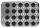
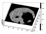
- 3 is a flowchart of a void evaluation method in solder according to the first embodiment. It is an example of a two-dimensional X-ray image.
- FIG. 5 is an image obtained by removing the influence of the coherent member of the substrate based on the two-dimensional X-ray image of FIG. 4.
- 6 is an image obtained by performing circle detection corresponding to a solder ball based on the image of FIG. 5. It is the image of the solder ball detected based on the image of FIG. It is an image in one solder.
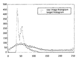
- FIG. 9 is an image obtained by enhancing the overall image contrast using the matching histogram equalization method for the image of FIG. 8. It is a graph which shows the histogram of the intensity
- strength about the image of FIG. 10, and a target histogram. 11 is an image obtained by enhancing the local contrast using an applicable histogram equalization method for the image of FIG. It is an image which represents intensity
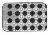
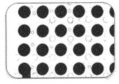
- FIG. 15 is an image reflecting the voids separated in FIG. 16. It is an example of the image which shows the void in each solder ball about a plurality of solder balls contained in a two-dimensional X-ray image. It is an example of the image obtained by setting so that only the void with a comparatively big influence may be shown.
- Evaluation device of voids in the solder for each pixel constituting an image in the solder, the pixel value p i included in the voids is 1 and the pixel value p i which is not included in the voids and 0
- An evaluation function calculation unit for calculating an evaluation function of the void i: Pixel number (1 to N) p i : Pixel value (0 or 1)
- a void evaluation unit that evaluates that the influence of the void is larger as the evaluation function is relatively larger; Is provided.
- the solder void evaluation apparatus may further include an image extraction unit that extracts an image in each solder from the two-dimensional X-ray image in the first aspect.
- the void evaluation apparatus in the solder according to the third aspect may further include a void detection unit that detects a void in the image in the solder.
- the weight function w (r i ) may be (r 0 ⁇ r i ). .
- the pixel value included in the void is set to 1
- the pixel value not included in the void is set to 0, and the center of the solder is set.
- the void evaluation method in the solder according to the sixth aspect is the step of extracting the image in each solder from the two-dimensional X-ray image in the fifth aspect, Detecting a void portion from an image in each solder; May further be included.
- the weighting function w (r i ) may be (r 0 ⁇ r i ).
- a computer program for evaluating voids in solder according to an eighth aspect causes a computer to execute the steps of the method for evaluating voids in solder according to any one of the fifth to seventh aspects, thereby causing voids in solder. Perform an evaluation.
- a computer-readable recording medium stores the solder void evaluation computer program according to the eighth aspect.
- FIG. 1 is a block diagram showing a functional configuration of the void evaluation apparatus in the solder according to the first embodiment.
- FIG. 2 is a block diagram illustrating a physical configuration of the void evaluation apparatus in the solder according to the first embodiment.
- the void evaluation apparatus 10 in the solder includes an evaluation function calculation unit 13 and a void evaluation unit 14 as functional configurations.
- the image extraction unit 11 extracts an image in each solder from the two-dimensional X-ray image.
- the void detection unit 12 detects a void in the image in each solder.
- Evaluation function calculation unit 13 for each pixel constituting an image in the solder, with its pixel value and the weighting function w (r i), and calculates the evaluation function within each solder.
- the void evaluation unit 14 evaluates that the influence of the void is larger as the evaluation function is relatively larger for each solder.
- the void evaluation device 10 in the solder includes a CPU 21, a memory 22, a storage device 23, an input / output unit 24, a display device 25, and an interface 26 as physical configurations. That is, the void evaluation apparatus 10 in the solder can be realized by a personal computer that operates software that realizes the functional configuration.
- the void in the solder can be automatically evaluated appropriately at high speed.
- the influence of voids in an actual solder ball appears as, for example, a connection failure because the bonding strength of the solder portion is reduced. It is considered that the voids in the solder cause cracks in the solder, resulting in poor connection and, consequently, malfunction of the entire device.
- the void evaluation device in the solder according to the first embodiment it is possible to suppress the occurrence of poor connection of the solder part.
- FIG. 4 is an example of a two-dimensional X-ray image.
- a general two-dimensional X-ray image has, for example, a 0-255 gradation bitmap format.
- the solder balls often interfere with other substrate members. For example, some joints produce a closed solder ball. Therefore, it is desirable to use a powerful segment extraction algorithm to handle various types of interfering background members.
- Removal of coherent member FIG. 5 is an image obtained by removing the influence of the coherent member on the substrate based on the two-dimensional X-ray image of FIG. In this case, an appropriate threshold value of intensity may be automatically set to reduce the interfering background.
- FIG. 6 is an image obtained by performing circle detection corresponding to the solder ball based on the image of FIG.
- the extraction of the position where the solder ball is likely may be performed using, for example, a Hough transform which is a circle detection algorithm.
- a circle radius value may be obtained by performing circle detection using a resized image instead of the original image and reducing the processing amount.
- the circle detection algorithm is not limited to the Hough transform, and other algorithms may be used.
- the solder shape is not a circle like a solder ball but a square or the like, another shape matching algorithm may be used.
- FIG. 7 is an image of a solder ball detected based on the image of FIG.
- a default radius range applied in the Hough transform may be expanded.
- an inappropriate ball that is, a portion that is not a solder ball is excluded, and an appropriate ball, that is, a portion that is considered to be a solder ball is finally selected.
- an image in each solder can be obtained from the two-dimensional X-ray image.
- the void detection unit 12 detects a void in the image in each solder.
- FIGS. 1 Original Image Intensity Distribution and Target Histogram
- FIG. 8 shows an image in one solder.
- FIG. 9 is a graph showing an intensity histogram and a target histogram for the image of FIG. Even if the voids appear bright in the solder ball in the image in one solder, it was actually difficult to detect these voids due to various factors. For example, factors such as bad image contrast, irregular shapes formed by overlapping voids, the size / position of various voids, and the influence of other members.
- FIG. 1 Original Image Intensity Distribution and Target Histogram
- FIG. 10 is an image obtained by enhancing the overall image contrast using the matching histogram equalization method for the image of FIG. .
- FIG. 11 is a graph showing an intensity histogram and a target histogram for the image of FIG. The quality of the image contrast varies according to various data acquisition settings.
- the input intensity conversion can enhance the overall image contrast and match the output intensity histogram to a desired target histogram with better contrast.
- FIG. 12 is an image obtained by enhancing the local contrast using the applicable histogram equalization method for the image of FIG.
- FIG. 13 is a three-dimensional image of the image of FIG.
- the local contrast of the local region may be improved by smoothing the image and then applying the contrast limited adaptive histogram equalization (CLAHE). .
- CLAHE contrast limited adaptive histogram equalization
- FIG. 14 is an image when the connected voids are erroneously detected as one connected void.
- FIG. 15 is a schematic diagram showing boundaries separating successive voids discovered by applying a water shedding algorithm to the image of FIG.
- the boundary of each void may be effectively determined by applying an appropriately sized edge detection algorithm (Laplacian of Gaussian filter). Sometimes a continuous void is mistakenly detected as a single connected void. Therefore, a boundary that separates consecutive voids can be found by applying a water shedding algorithm.
- the edge detection algorithm is not limited to the water shedding algorithm, and other algorithms may be used.
- FIG. 16 is a diagram in which only the voids are extracted from the image of FIG. 15 and the connected voids are separated by boundaries.
- FIG. 17 is an image in which the voids separated in FIG. 16 are reflected on the image of FIG.
- a two-dimensional X-ray image is binarized by setting an appropriate threshold value, and voids are detected using Betti numbers, which are topological information included in the binary image. Yes.
- a morphological operation is performed to remove the connected locations and completely separate the connected voids. As described above, a void portion in each solder can be detected.
- the evaluation function is as follows. i: Pixel number (1 to N) r i : Distance from the solder center of the i-th pixel p i : Pixel value of the i-th pixel (0 or 1) w (ri): weight function
- i is a pixel number, which is number 1 to number N.
- p i is each pixel value and takes 0 or 1.
- the weight function w (r i ) may be determined depending on what function the influence of the void is expressed with respect to the distance r i from the BGA center. The present inventor considered that the influence becomes larger as the void position is closer to the center of the BGA, and that the influence becomes 0 when the maximum radius (r 0 ) of the BGA is exceeded. It is a thing.
- the weighting function w (r i ) may be (r 0 ⁇ r i ).
- the evaluation function in this case can be expressed as the following equation (2).
- a matching weight function may be selected.
- a quadratic function ((r 0 ⁇ r i ) 2 ) or a higher order function may be selected.
- the evaluation may be performed for each void.
- the area S j of each void may be evaluated. This may be calculated assuming that S j pixels are gathered at the center of the void.
- the evaluation function is represented by the following expression (3). j: Void number (1 to M) r j : pixel at the center of the j th void S j : area of the j th void, here expressed as the number of pixels contained in the void.
- the pixels included in the void are processed not for individual pixels but for the void area Sj for the center of the j-th void.
- the equation for all pixels is the same as the above equation (2).
- the denominator may be treated as a constant.
- the evaluation function is as follows.
- the evaluation function is not limited to those shown in the above formulas (1) to (5).
- the void evaluation unit 14 evaluates that the influence of the void is larger as the evaluation function is relatively larger for each solder.
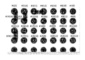
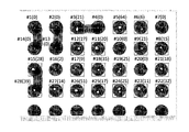
- FIG. 18 is an example of an image showing a void in each solder ball for a plurality of solder balls included in the two-dimensional X-ray image.
- FIG. 19 is an example of an image obtained by performing settings so as to show only voids having a relatively large influence. 18 and 19 are images in a plurality of solder balls included in the two-dimensional X-ray image, respectively. Detected voids are shown in each solder.
- each solder can be compared with the conventional method by calculating an evaluation function using a weight function that takes into account voids having a large influence. It is possible to accurately evaluate the influence of voids at a high speed.
- the void evaluation method according to the first embodiment is characterized in that voids in solder are evaluated by an evaluation function weighted by a weight function w (ri) for the distance ri from the BGA center of the void.
- FIG. 3 is a flowchart of the void evaluation method in the solder according to the first embodiment.
- the void evaluation method in the solder includes the following steps. (A) An image in each solder is extracted from the two-dimensional X-ray image (S01). (B) A void is detected for the image in each solder (S01).
- the value of the evaluation function is to evaluate the large influence of the more relatively large void (S03).
- the voids in each solder can be automatically evaluated appropriately at high speed.
- effect According to the void evaluation method in the solder according to the present invention, the void in the solder can be automatically evaluated appropriately at high speed.
- a computer program for evaluating voids in solder for causing the computer to execute each step of the method for evaluating voids in solder and evaluating voids in solder can be provided.
- the in-solder void evaluation computer program may be stored in a computer-readable recording medium.
- the computer-readable recording medium is, for example, a magnetic recording medium such as a flexible disk or a magnetic tape, an optical recording medium such as a compact disk (CD), a digital versatile disk (DVD), or a Blu-ray (registered trademark) disk (BD). Any of semiconductor storage media such as a magneto-optical recording medium, a USB memory, and a flash memory may be used.
- the void in the solder can be automatically evaluated appropriately at high speed. Therefore, it is useful for applications such as a soldered circuit board evaluation device or a semiconductor device manufacturing device including these.
Landscapes
- Engineering & Computer Science (AREA)
- Physics & Mathematics (AREA)
- General Physics & Mathematics (AREA)
- Chemical & Material Sciences (AREA)
- Biochemistry (AREA)
- Theoretical Computer Science (AREA)
- Health & Medical Sciences (AREA)
- Life Sciences & Earth Sciences (AREA)
- Quality & Reliability (AREA)
- Analytical Chemistry (AREA)
- Computer Vision & Pattern Recognition (AREA)
- General Health & Medical Sciences (AREA)
- Immunology (AREA)
- Pathology (AREA)
- Manufacturing & Machinery (AREA)
- Microelectronics & Electronic Packaging (AREA)
- Analysing Materials By The Use Of Radiation (AREA)
- Length-Measuring Devices Using Wave Or Particle Radiation (AREA)
- Electric Connection Of Electric Components To Printed Circuits (AREA)
Priority Applications (1)
| Application Number | Priority Date | Filing Date | Title |
|---|---|---|---|
| US15/034,302 US9965849B2 (en) | 2013-11-15 | 2014-11-10 | Void evaluation apparatus and void evaluation method in the solder |
Applications Claiming Priority (2)
| Application Number | Priority Date | Filing Date | Title |
|---|---|---|---|
| JP2013237024A JP6360674B2 (ja) | 2013-11-15 | 2013-11-15 | ハンダ内のボイドの評価装置及びハンダ内のボイドの評価方法 |
| JP2013-237024 | 2013-11-15 |
Publications (1)
| Publication Number | Publication Date |
|---|---|
| WO2015072424A1 true WO2015072424A1 (ja) | 2015-05-21 |
Family
ID=53057358
Family Applications (1)
| Application Number | Title | Priority Date | Filing Date |
|---|---|---|---|
| PCT/JP2014/079717 Ceased WO2015072424A1 (ja) | 2013-11-15 | 2014-11-10 | ハンダ内のボイドの評価装置及びハンダ内のボイドの評価方法 |
Country Status (3)
| Country | Link |
|---|---|
| US (1) | US9965849B2 (https=) |
| JP (1) | JP6360674B2 (https=) |
| WO (1) | WO2015072424A1 (https=) |
Cited By (1)
| Publication number | Priority date | Publication date | Assignee | Title |
|---|---|---|---|---|
| JP2023057471A (ja) * | 2021-10-11 | 2023-04-21 | Jfeスチール株式会社 | 耐火物の欠陥評価方法 |
Families Citing this family (2)
| Publication number | Priority date | Publication date | Assignee | Title |
|---|---|---|---|---|
| JP2020159758A (ja) * | 2019-03-25 | 2020-10-01 | 豊田合成株式会社 | 発光装置の製造方法および半田接合部検査装置 |
| JP7728536B2 (ja) * | 2020-01-15 | 2025-08-25 | 株式会社クオルテック | 電子部品を接続する接合部のボイド・クラックの検出方法 |
Citations (2)
| Publication number | Priority date | Publication date | Assignee | Title |
|---|---|---|---|---|
| JP2004198206A (ja) * | 2002-12-17 | 2004-07-15 | Toyota Motor Corp | 電子部品の放熱性検査方法及びその装置 |
| JP2007121082A (ja) * | 2005-10-27 | 2007-05-17 | Nagoya Electric Works Co Ltd | X線画像出力装置、x線画像出力方法およびx線画像出力プログラム |
Family Cites Families (5)
| Publication number | Priority date | Publication date | Assignee | Title |
|---|---|---|---|---|
| CN1409816A (zh) * | 1999-11-08 | 2003-04-09 | 泰瑞达因公司 | 利用垂直断层成像的检查方法 |
| JP4631460B2 (ja) | 2005-02-18 | 2011-02-16 | パナソニック株式会社 | X線検査方法 |
| JP2011075470A (ja) * | 2009-10-01 | 2011-04-14 | Fujitsu Ltd | 画像処理プログラム、画像処理方法および画像処理装置 |
| US8306311B2 (en) * | 2010-04-14 | 2012-11-06 | Oracle International Corporation | Method and system for automated ball-grid array void quantification |
| CN104428881B (zh) * | 2013-07-08 | 2017-06-09 | 索尼公司 | 固化条件的确定方法、电路器件的生产方法和电路器件 |
-
2013
- 2013-11-15 JP JP2013237024A patent/JP6360674B2/ja active Active
-
2014
- 2014-11-10 US US15/034,302 patent/US9965849B2/en active Active
- 2014-11-10 WO PCT/JP2014/079717 patent/WO2015072424A1/ja not_active Ceased
Patent Citations (2)
| Publication number | Priority date | Publication date | Assignee | Title |
|---|---|---|---|---|
| JP2004198206A (ja) * | 2002-12-17 | 2004-07-15 | Toyota Motor Corp | 電子部品の放熱性検査方法及びその装置 |
| JP2007121082A (ja) * | 2005-10-27 | 2007-05-17 | Nagoya Electric Works Co Ltd | X線画像出力装置、x線画像出力方法およびx線画像出力プログラム |
Cited By (2)
| Publication number | Priority date | Publication date | Assignee | Title |
|---|---|---|---|---|
| JP2023057471A (ja) * | 2021-10-11 | 2023-04-21 | Jfeスチール株式会社 | 耐火物の欠陥評価方法 |
| JP7708639B2 (ja) | 2021-10-11 | 2025-07-15 | Jfeスチール株式会社 | 耐火物の欠陥評価方法 |
Also Published As
| Publication number | Publication date |
|---|---|
| US20160267646A1 (en) | 2016-09-15 |
| JP6360674B2 (ja) | 2018-07-18 |
| US9965849B2 (en) | 2018-05-08 |
| JP2015096836A (ja) | 2015-05-21 |
Similar Documents
| Publication | Publication Date | Title |
|---|---|---|
| CN106446952B (zh) | 一种乐谱图像识别方法及装置 | |
| WO2019057067A1 (zh) | 图像质量评估方法及装置 | |
| CN110288566B (zh) | 一种目标缺陷提取方法 | |
| CN111815660B (zh) | 危化品仓库中货物边缘检测方法、装置及终端设备 | |
| CN105469027A (zh) | 针对文档图像的水平和垂直线检测和移除 | |
| CN112437948A (zh) | 图像诊断支援系统及图像诊断支援装置 | |
| CN119804490B (zh) | 一种基于图像识别的印制线路板缺陷检测方法及系统 | |
| CN116542982A (zh) | 一种基于机器视觉的出发判断器缺陷检测方法及装置 | |
| CN110688871A (zh) | 一种基于条码识别的边缘检测方法 | |
| CN110085529B (zh) | 检测方法、检测设备和计算机可读存储介质 | |
| JP6360674B2 (ja) | ハンダ内のボイドの評価装置及びハンダ内のボイドの評価方法 | |
| CN115457375A (zh) | 水下障碍物图像识别方法、系统、电子设备以及计算机可读介质 | |
| CN110728692A (zh) | 一种基于Scharr算子改进的图像边缘检测方法 | |
| CN117765014A (zh) | 图像边缘检测方法、装置、设备以及存储介质 | |
| CN103793902A (zh) | 管型识别方法和装置、以及尿液分析仪 | |
| CN114913112A (zh) | 晶圆双边缘检测方法和装置及设备 | |
| KR101527962B1 (ko) | 비디오 영상의 움직임 객체 추출 방법 | |
| KR101615479B1 (ko) | 적응적 전/후처리 필터링을 이용하는 초해상도 영상 처리 방법 | |
| CN109934817B (zh) | 一种果体外部轮廓畸形检测方法 | |
| US8655061B2 (en) | Image processing apparatus and image processing method for performing a convolution operation | |
| CN114845041B (zh) | 一种用于纳米颗粒成像的对焦方法、装置及存储介质 | |
| JP6095050B2 (ja) | テクスチャ検出装置、テクスチャ検出方法、テクスチャ検出プログラム及び画像処理システム | |
| US7646892B2 (en) | Image inspecting apparatus, image inspecting method, control program and computer-readable storage medium | |
| CN115731185A (zh) | 基于拉普拉斯算子的电力设备模糊图像识别方法及系统 | |
| CN115862044A (zh) | 用于从图像中提取目标文档部分的方法、设备和介质 |
Legal Events
| Date | Code | Title | Description |
|---|---|---|---|
| 121 | Ep: the epo has been informed by wipo that ep was designated in this application |
Ref document number: 14861850 Country of ref document: EP Kind code of ref document: A1 |
|
| WWE | Wipo information: entry into national phase |
Ref document number: 15034302 Country of ref document: US |
|
| NENP | Non-entry into the national phase |
Ref country code: DE |
|
| 122 | Ep: pct application non-entry in european phase |
Ref document number: 14861850 Country of ref document: EP Kind code of ref document: A1 |