WO2015064432A1 - 有機エレクトロルミネッセンス素子、及び、有機エレクトロルミネッセンス表示パネル - Google Patents
有機エレクトロルミネッセンス素子、及び、有機エレクトロルミネッセンス表示パネル Download PDFInfo
- Publication number
- WO2015064432A1 WO2015064432A1 PCT/JP2014/078024 JP2014078024W WO2015064432A1 WO 2015064432 A1 WO2015064432 A1 WO 2015064432A1 JP 2014078024 W JP2014078024 W JP 2014078024W WO 2015064432 A1 WO2015064432 A1 WO 2015064432A1
- Authority
- WO
- WIPO (PCT)
- Prior art keywords
- layer
- light emitting
- light
- organic
- display panel
- Prior art date
- Legal status (The legal status is an assumption and is not a legal conclusion. Google has not performed a legal analysis and makes no representation as to the accuracy of the status listed.)
- Ceased
Links
Images







Classifications
-
- H—ELECTRICITY
- H10—SEMICONDUCTOR DEVICES; ELECTRIC SOLID-STATE DEVICES NOT OTHERWISE PROVIDED FOR
- H10K—ORGANIC ELECTRIC SOLID-STATE DEVICES
- H10K50/00—Organic light-emitting devices
- H10K50/10—OLEDs or polymer light-emitting diodes [PLED]
- H10K50/11—OLEDs or polymer light-emitting diodes [PLED] characterised by the electroluminescent [EL] layers
-
- H—ELECTRICITY
- H10—SEMICONDUCTOR DEVICES; ELECTRIC SOLID-STATE DEVICES NOT OTHERWISE PROVIDED FOR
- H10K—ORGANIC ELECTRIC SOLID-STATE DEVICES
- H10K50/00—Organic light-emitting devices
- H10K50/10—OLEDs or polymer light-emitting diodes [PLED]
- H10K50/14—Carrier transporting layers
- H10K50/15—Hole transporting layers
-
- H—ELECTRICITY
- H10—SEMICONDUCTOR DEVICES; ELECTRIC SOLID-STATE DEVICES NOT OTHERWISE PROVIDED FOR
- H10K—ORGANIC ELECTRIC SOLID-STATE DEVICES
- H10K50/00—Organic light-emitting devices
- H10K50/10—OLEDs or polymer light-emitting diodes [PLED]
- H10K50/14—Carrier transporting layers
- H10K50/16—Electron transporting layers
- H10K50/165—Electron transporting layers comprising dopants
-
- H—ELECTRICITY
- H10—SEMICONDUCTOR DEVICES; ELECTRIC SOLID-STATE DEVICES NOT OTHERWISE PROVIDED FOR
- H10K—ORGANIC ELECTRIC SOLID-STATE DEVICES
- H10K2101/00—Properties of the organic materials covered by group H10K85/00
- H10K2101/10—Triplet emission
-
- H—ELECTRICITY
- H10—SEMICONDUCTOR DEVICES; ELECTRIC SOLID-STATE DEVICES NOT OTHERWISE PROVIDED FOR
- H10K—ORGANIC ELECTRIC SOLID-STATE DEVICES
- H10K2101/00—Properties of the organic materials covered by group H10K85/00
- H10K2101/30—Highest occupied molecular orbital [HOMO], lowest unoccupied molecular orbital [LUMO] or Fermi energy values
-
- H—ELECTRICITY
- H10—SEMICONDUCTOR DEVICES; ELECTRIC SOLID-STATE DEVICES NOT OTHERWISE PROVIDED FOR
- H10K—ORGANIC ELECTRIC SOLID-STATE DEVICES
- H10K2101/00—Properties of the organic materials covered by group H10K85/00
- H10K2101/40—Interrelation of parameters between multiple constituent active layers or sublayers, e.g. HOMO values in adjacent layers
-
- H—ELECTRICITY
- H10—SEMICONDUCTOR DEVICES; ELECTRIC SOLID-STATE DEVICES NOT OTHERWISE PROVIDED FOR
- H10K—ORGANIC ELECTRIC SOLID-STATE DEVICES
- H10K2102/00—Constructional details relating to the organic devices covered by this subclass
-
- H—ELECTRICITY
- H10—SEMICONDUCTOR DEVICES; ELECTRIC SOLID-STATE DEVICES NOT OTHERWISE PROVIDED FOR
- H10K—ORGANIC ELECTRIC SOLID-STATE DEVICES
- H10K2102/00—Constructional details relating to the organic devices covered by this subclass
- H10K2102/10—Transparent electrodes, e.g. using graphene
- H10K2102/101—Transparent electrodes, e.g. using graphene comprising transparent conductive oxides [TCO]
- H10K2102/103—Transparent electrodes, e.g. using graphene comprising transparent conductive oxides [TCO] comprising indium oxides, e.g. ITO
-
- H—ELECTRICITY
- H10—SEMICONDUCTOR DEVICES; ELECTRIC SOLID-STATE DEVICES NOT OTHERWISE PROVIDED FOR
- H10K—ORGANIC ELECTRIC SOLID-STATE DEVICES
- H10K2102/00—Constructional details relating to the organic devices covered by this subclass
- H10K2102/301—Details of OLEDs
- H10K2102/302—Details of OLEDs of OLED structures
- H10K2102/3023—Direction of light emission
- H10K2102/3026—Top emission
-
- H—ELECTRICITY
- H10—SEMICONDUCTOR DEVICES; ELECTRIC SOLID-STATE DEVICES NOT OTHERWISE PROVIDED FOR
- H10K—ORGANIC ELECTRIC SOLID-STATE DEVICES
- H10K2102/00—Constructional details relating to the organic devices covered by this subclass
- H10K2102/301—Details of OLEDs
- H10K2102/351—Thickness
-
- H—ELECTRICITY
- H10—SEMICONDUCTOR DEVICES; ELECTRIC SOLID-STATE DEVICES NOT OTHERWISE PROVIDED FOR
- H10K—ORGANIC ELECTRIC SOLID-STATE DEVICES
- H10K50/00—Organic light-emitting devices
- H10K50/10—OLEDs or polymer light-emitting diodes [PLED]
- H10K50/14—Carrier transporting layers
- H10K50/16—Electron transporting layers
-
- H—ELECTRICITY
- H10—SEMICONDUCTOR DEVICES; ELECTRIC SOLID-STATE DEVICES NOT OTHERWISE PROVIDED FOR
- H10K—ORGANIC ELECTRIC SOLID-STATE DEVICES
- H10K50/00—Organic light-emitting devices
- H10K50/10—OLEDs or polymer light-emitting diodes [PLED]
- H10K50/17—Carrier injection layers
-
- H—ELECTRICITY
- H10—SEMICONDUCTOR DEVICES; ELECTRIC SOLID-STATE DEVICES NOT OTHERWISE PROVIDED FOR
- H10K—ORGANIC ELECTRIC SOLID-STATE DEVICES
- H10K50/00—Organic light-emitting devices
- H10K50/10—OLEDs or polymer light-emitting diodes [PLED]
- H10K50/17—Carrier injection layers
- H10K50/171—Electron injection layers
-
- H—ELECTRICITY
- H10—SEMICONDUCTOR DEVICES; ELECTRIC SOLID-STATE DEVICES NOT OTHERWISE PROVIDED FOR
- H10K—ORGANIC ELECTRIC SOLID-STATE DEVICES
- H10K50/00—Organic light-emitting devices
- H10K50/80—Constructional details
- H10K50/805—Electrodes
- H10K50/82—Cathodes
- H10K50/828—Transparent cathodes, e.g. comprising thin metal layers
-
- H—ELECTRICITY
- H10—SEMICONDUCTOR DEVICES; ELECTRIC SOLID-STATE DEVICES NOT OTHERWISE PROVIDED FOR
- H10K—ORGANIC ELECTRIC SOLID-STATE DEVICES
- H10K59/00—Integrated devices, or assemblies of multiple devices, comprising at least one organic light-emitting element covered by group H10K50/00
- H10K59/10—OLED displays
- H10K59/12—Active-matrix OLED [AMOLED] displays
-
- H—ELECTRICITY
- H10—SEMICONDUCTOR DEVICES; ELECTRIC SOLID-STATE DEVICES NOT OTHERWISE PROVIDED FOR
- H10K—ORGANIC ELECTRIC SOLID-STATE DEVICES
- H10K59/00—Integrated devices, or assemblies of multiple devices, comprising at least one organic light-emitting element covered by group H10K50/00
- H10K59/80—Constructional details
- H10K59/805—Electrodes
- H10K59/8052—Cathodes
- H10K59/80524—Transparent cathodes, e.g. comprising thin metal layers
-
- H—ELECTRICITY
- H10—SEMICONDUCTOR DEVICES; ELECTRIC SOLID-STATE DEVICES NOT OTHERWISE PROVIDED FOR
- H10K—ORGANIC ELECTRIC SOLID-STATE DEVICES
- H10K85/00—Organic materials used in the body or electrodes of devices covered by this subclass
- H10K85/30—Coordination compounds
- H10K85/341—Transition metal complexes, e.g. Ru(II)polypyridine complexes
- H10K85/342—Transition metal complexes, e.g. Ru(II)polypyridine complexes comprising iridium
-
- H—ELECTRICITY
- H10—SEMICONDUCTOR DEVICES; ELECTRIC SOLID-STATE DEVICES NOT OTHERWISE PROVIDED FOR
- H10K—ORGANIC ELECTRIC SOLID-STATE DEVICES
- H10K85/00—Organic materials used in the body or electrodes of devices covered by this subclass
- H10K85/60—Organic compounds having low molecular weight
- H10K85/615—Polycyclic condensed aromatic hydrocarbons, e.g. anthracene
- H10K85/626—Polycyclic condensed aromatic hydrocarbons, e.g. anthracene containing more than one polycyclic condensed aromatic rings, e.g. bis-anthracene
-
- H—ELECTRICITY
- H10—SEMICONDUCTOR DEVICES; ELECTRIC SOLID-STATE DEVICES NOT OTHERWISE PROVIDED FOR
- H10K—ORGANIC ELECTRIC SOLID-STATE DEVICES
- H10K85/00—Organic materials used in the body or electrodes of devices covered by this subclass
- H10K85/60—Organic compounds having low molecular weight
- H10K85/631—Amine compounds having at least two aryl rest on at least one amine-nitrogen atom, e.g. triphenylamine
- H10K85/633—Amine compounds having at least two aryl rest on at least one amine-nitrogen atom, e.g. triphenylamine comprising polycyclic condensed aromatic hydrocarbons as substituents on the nitrogen atom
-
- H—ELECTRICITY
- H10—SEMICONDUCTOR DEVICES; ELECTRIC SOLID-STATE DEVICES NOT OTHERWISE PROVIDED FOR
- H10K—ORGANIC ELECTRIC SOLID-STATE DEVICES
- H10K85/00—Organic materials used in the body or electrodes of devices covered by this subclass
- H10K85/60—Organic compounds having low molecular weight
- H10K85/631—Amine compounds having at least two aryl rest on at least one amine-nitrogen atom, e.g. triphenylamine
- H10K85/636—Amine compounds having at least two aryl rest on at least one amine-nitrogen atom, e.g. triphenylamine comprising heteroaromatic hydrocarbons as substituents on the nitrogen atom
-
- H—ELECTRICITY
- H10—SEMICONDUCTOR DEVICES; ELECTRIC SOLID-STATE DEVICES NOT OTHERWISE PROVIDED FOR
- H10K—ORGANIC ELECTRIC SOLID-STATE DEVICES
- H10K85/00—Organic materials used in the body or electrodes of devices covered by this subclass
- H10K85/60—Organic compounds having low molecular weight
- H10K85/649—Aromatic compounds comprising a hetero atom
- H10K85/657—Polycyclic condensed heteroaromatic hydrocarbons
- H10K85/6572—Polycyclic condensed heteroaromatic hydrocarbons comprising only nitrogen in the heteroaromatic polycondensed ring system, e.g. phenanthroline or carbazole
Definitions
- the present invention relates to an organic electroluminescence element (hereinafter also referred to as “organic EL element”) and an organic electroluminescence display panel (hereinafter also referred to as “organic EL display panel”). More specifically, the present invention relates to an organic EL element having high luminous efficiency and an organic EL display panel including the organic EL element.
- organic EL element organic electroluminescence element
- organic EL display panel organic electroluminescence display panel
- organic EL elements using electroluminescence of organic materials have attracted attention as display elements used in thin display devices.
- the organic EL element emits light by recombining holes injected from an anode and electrons injected from a cathode in a light emitting layer disposed between both electrodes.
- Such a self-luminous organic EL element has excellent characteristics such as high luminance light emission, high-speed response, wide viewing angle, thin and light weight, and is applied to various fields such as display panels and lighting. Is expected.
- the light emitting layer of the organic EL element a layer in which a light emitting dopant material mainly responsible for light emission and a light emitting host material mainly responsible for transport of holes and electrons is usually mixed by co-evaporation. With respect to such a configuration, it has been studied to further increase the functionality of the organic EL element, and examples thereof include the following.
- an organic EL element in which a layer having a light emitting dopant material concentration of 100% by weight is arranged is known (for example, see Patent Document 1).
- an organic EL element in which a layer containing a light emitting host material as a main component and not containing a light emitting dopant material is known (see, for example, Patent Document 2).
- an organic EL composed of a fluorescent organic compound that emits light by acting as a recombination center, and in which an island-shaped thin film having an average film thickness smaller than the thickness of a monomolecular film of the fluorescent organic compound is arranged
- An element is known (see, for example, Patent Document 3).
- an organic EL element in which a metal doping layer doped with a metal or a metal salt is disposed between an organic compound layer disposed between an anode and a cathode and the cathode (for example, Patent Documents 4 and 5).
- an organic EL element in which a material constituting a normal light emitting layer has predetermined characteristics, and a barrier layer having predetermined characteristics is disposed (see, for example, Patent Document 6).
- an organic EL element in which a plurality of layers are stacked with the characteristics of materials constituting a normal light emitting layer being predetermined (see, for example, Patent Documents 7 and 8).
- an organic EL element in which an efficiency enhancement layer is disposed is known (for example, see Non-Patent Documents 1 and 2).
- an organic EL element when a light emitting layer in which a light emitting host material and a light emitting dopant material are mixed is used, the light emitting region is widened and the light emission efficiency may be lowered.
- a triplet-triplet fusion (TTF) phenomenon is unlikely to occur and the luminous efficiency may not be increased. The reason for this will be described below.
- FIG. 16 is a schematic cross-sectional view showing a conventional organic EL display panel.
- the organic EL display panel 101 c includes a substrate 2 and an organic EL element 103 c disposed on the substrate 2.
- the organic EL element 103c has an anode 4, a hole transport layer 7, a light emitting layer 108b, an electron transport layer 9, and a cathode 5 in this order from the substrate 2 side.
- the light emitting layer 108b has a configuration in which the light emitting dopant material 19 and the light emitting host material 20 are mixed by co-evaporation. In this case, since the light emitting dopant material 19 is dispersed throughout the light emitting layer 108b, the light emitting region ER3 of the organic EL element 103c extends over the entire light emitting layer 108b as shown in FIG.
- the organic EL element 103c since the light emitting region ER3 spreads over the entire light emitting layer 108b, the density of excitons may be reduced and the light emission efficiency may be lowered. In particular, when delayed fluorescence is used with a blue fluorescent material, the TTF phenomenon is less likely to occur and the luminous efficiency may be reduced.
- the light-emitting layer 108b is formed by co-evaporation of the light-emitting dopant material 19 and the light-emitting host material 20, it is difficult to control the deposition rate so as to achieve a desired weight ratio of each material. In some cases, the production efficiency may be reduced.
- the conventional organic EL element 103c has room for improvement in that the luminous efficiency is sufficiently increased and the manufacturing efficiency is excellent.
- Patent Document 1 discloses that an organic EL element with low driving voltage and high luminous efficiency is provided.
- the invention described in Patent Document 1 has a light emitting layer in which a light emitting dopant material and a light emitting host material are mixed as shown in FIG. There was room for ingenuity in the point to raise.
- a light emitting layer is formed by co-evaporation of a light emitting dopant material and a light emitting host material, there is room for improvement in terms of improving manufacturing efficiency.
- Patent Document 2 discloses that an organic EL element that can be driven at a low voltage without impairing durability is provided.
- the invention described in Patent Document 2 has a light-emitting layer in which a light-emitting dopant material and a light-emitting host material are mixed, as shown in FIG. There was room for ingenuity in the point to raise.
- a light emitting layer is formed by co-evaporation of a light emitting dopant material and a light emitting host material, there is room for improvement in terms of improving manufacturing efficiency.
- Patent Document 3 discloses that an organic EL element having a new layer structure and capable of effectively utilizing a fluorescent organic compound is provided.
- an island-shaped thin film responsible for light emission is disposed between the hole transport layer and the electron transport layer, and in a region where the island-shaped thin film is not distributed, hole transport is performed. Since the layer and the electron transport layer are directly connected, recombination of holes and electrons does not occur in the island-shaped thin film, and as a result, the light emission efficiency may be reduced. Therefore, the invention described in Patent Document 3 has room for improvement in terms of sufficiently increasing the light emission efficiency.
- Patent Document 4 discloses that an organic EL element having a low driving voltage and capable of producing a high-efficiency, high-luminance light-emitting element is provided.
- the invention described in Patent Document 4 has a light-emitting layer in which a light-emitting dopant material and a light-emitting host material are mixed as shown in FIG. There was room for ingenuity in the point to raise.
- a light emitting layer is formed by co-evaporation of a light emitting dopant material and a light emitting host material, there is room for improvement in terms of improving manufacturing efficiency.
- Patent Document 5 discloses that an organic EL element capable of reducing the driving voltage and controlling the emission spectrum is provided.
- the invention described in Patent Document 5 has a light-emitting layer in which a light-emitting dopant material and a light-emitting host material are mixed as shown in FIG. There was room for ingenuity in the point to raise.
- a light emitting layer is formed by co-evaporation of a light emitting dopant material and a light emitting host material, there is room for improvement in terms of improving manufacturing efficiency.
- Patent Document 6 discloses that a TTF phenomenon is efficiently caused inside the light emitting layer to provide a highly efficient organic EL element that greatly exceeds the internal quantum efficiency of 25%, which is said to be a limit value of a conventional fluorescent element. Yes. However, since the TTF phenomenon occurs between two excitons, it is considered that the TTF phenomenon is less likely to occur when the concentration of the luminescent dopant material is low. Therefore, the invention described in Patent Document 6 has room for improvement in terms of sufficiently increasing the light emission efficiency. The same applies to Non-Patent Documents 1 and 2 above.
- the present invention has been made in view of the above situation, and includes an organic EL element capable of sufficiently increasing luminous efficiency and excellent manufacturing efficiency, and an organic EL display panel including the organic EL element. It is intended to provide.
- the inventors of the present invention have made various studies on organic EL elements that can sufficiently increase the luminous efficiency and have excellent manufacturing efficiency.
- the light-emitting layer contains a light-emitting dopant material and a light-emitting host material in separate layers.
- the configuration By adopting such a configuration, the light emitting region can be limited to a narrow region near the interface between the light emitting dopant layer composed of the light emitting dopant material and the light emitting host layer composed of the light emitting host material. It has been found that the density of excitons can be increased and the luminous efficiency can be increased.
- the excitation light emission between the light-emitting dopant material and the light-emitting host material can also be utilized, and thereby the light emission efficiency can be increased.
- the light emitting layer can be formed without co-evaporating the light emitting dopant material and the light emitting host material, it has been found that the production efficiency can be improved.
- one embodiment of the present invention is an organic electroluminescent element including an anode, a light emitting layer, and a cathode in order, the light emitting layer having a light emitting dopant layer and a light emitting host layer, and the light emitting dopant layer is
- the organic light-emitting device may contain an emission dopant material and substantially no emission host material, and the emission host layer may contain an emission host material and substantially no emission dopant material.
- Another embodiment of the present invention may be an organic electroluminescence display panel including a substrate and the organic electroluminescence element disposed on the substrate.
- FIG. 1 is a schematic cross-sectional view showing an organic EL display panel of Example 1.
- FIG. It is explanatory drawing explaining the drive principle of the organic EL element in FIG. 6 is a schematic cross-sectional view showing an organic EL display panel of Example 2.
- FIG. It is explanatory drawing explaining the drive principle of the organic EL element in FIG. 6 is a schematic cross-sectional view showing an organic EL display panel of Example 3.
- FIG. 6 is a schematic cross-sectional view showing an organic EL display panel of Comparative Example 1.
- FIG. 10 is a schematic cross-sectional view showing an organic EL display panel of Comparative Example 2.
- FIG. 6 is a schematic cross-sectional view showing an organic EL display panel of Example 4.
- FIG. 6 is a schematic cross-sectional view showing an organic EL display panel of Example 5.
- FIG. 10 is a schematic cross-sectional view showing an organic EL display panel of Example 6.
- FIG. 10 is a schematic cross-sectional view showing an organic EL display panel of Example 7.
- FIG. 10 is a band correlation diagram on the cathode side of the organic EL display panel of Example 7.
- 10 is a schematic cross-sectional view showing an organic EL display panel of Example 8.
- FIG. 10 is a band correlation diagram on the cathode side of the organic EL display panel of Example 8.
- 10 is a schematic cross-sectional view showing an organic EL display panel of Example 9.
- FIG. It is a cross-sectional schematic diagram which shows the conventional organic EL display panel.
- the light emitting layer includes a light emitting dopant layer and a light emitting host layer.
- the light emitting host layer may be a single layer or may be composed of a plurality of layers.
- the plurality of layers constituting the light-emitting host layer may have a layer containing a small amount of a light-emitting dopant material in a part thereof, as long as the effect of the present invention is not impaired, and the concentration is changed in the layer. Also good. In this case, the concentration of the light-emitting dopant material is preferably 20% by weight or less.
- organic electroluminescence is also described as “organic EL”.
- the organic EL is also referred to as an organic light emitting diode (OLED: Organic Light Emitting Diode).
- Example 1 relates to an organic EL element including an anode, a light-emitting layer, and a cathode in order from the substrate side, and an organic EL display panel including the organic EL element.
- the light-emitting layer has a light-emitting dopant layer on the anode side.
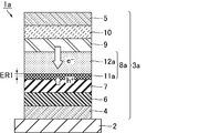
- FIG. 1 is a schematic cross-sectional view showing an organic EL display panel of Example 1.
- the organic EL display panel 1 a includes a substrate 2 and an organic EL element 3 a disposed on the substrate 2.
- the organic EL element 3a includes an anode 4, a hole injection layer 6, a hole transport layer 7, a light emitting layer 8a, an electron transport layer 9, an electron injection layer 10, and a cathode 5 in this order from the substrate 2 side.
- the light emitting layer 8a has a light emitting dopant layer 11a on the anode 4 side and a light emitting host layer 12a on the cathode 5 side.
- the substrate 2 an active matrix substrate having a thin film transistor element was used, and the organic EL element 3a was driven by connecting the anode 4 and the thin film transistor element.
- a transparent substrate or the like can be used as the substrate 2.
- the transparent substrate include a glass substrate and a plastic substrate.
- a foldable plastic substrate is used as the transparent substrate, a flexible organic EL display panel can be obtained.
- the organic EL display panel 1a of Example 1 is a top emission type in which light is emitted from the cathode 5 side when the anode 4 has light reflectivity and the cathode 5 has light transmittance.
- an aluminum (Al) and indium zinc oxide (IZO: Indium Zinc Oxide) layered in order from the substrate 2 side is used (hereinafter also referred to as “Al / IZO”), and the thickness thereof is used. Is, for example, 50 nm.
- the electrode having light reflectivity for example, Al, indium (In), or the like can be used.
- indium tin oxide ITO: Indium Tin Oxide
- its thickness is, for example, 100 nm.
- ITO was deposited by sputtering.
- IZO or the like can be used as the electrode having optical transparency.
- hole injection layer 6 4,4′-bis [N- (1-naphthyl) -N-phenyl-amino] -biphenyl ( ⁇ -NPD) and molybdenum trioxide (MoO 3 ) in a weight ratio of 80: What was co-evaporated at 20 is used, and its thickness is, for example, 40 nm.
- a layer possessed by a normal organic EL element can be used.
- hole transport layer 7 As the hole transport layer 7, ⁇ -NPD is used, and the thickness thereof is, for example, 30 nm. As the hole transport layer 7, a layer possessed by a normal organic EL element can be used.
- buthophenanthroline (Bphen) is used, and its thickness is, for example, 15 nm.
- the electron transport layer 9 what a normal organic EL element has can be used.
- lithium fluoride LiF
- the thickness thereof is, for example, 1 nm.
- a normal organic EL element can be used.
- a light emitting dopant material constituting the light emitting dopant layer 11a a diamine pyrene-based blue delayed fluorescent material was used, and its concentration was set to 100% by weight.
- the thickness of the light emitting dopant layer 11a is, for example, 0.1 nm.
- the luminescent dopant material either a fluorescent dopant material or a phosphorescent dopant material can be used.
- the phosphorescent dopant material include tris (2-phenylpyridinate) iridium (III) (Ir (ppy) 3) and the like. Is mentioned.
- the light emitting dopant layer 11a does not substantially contain the light emitting host material, and may contain, for example, a trace amount of impurities other than the light emitting dopant material.
- the fact that the light emitting dopant layer does not substantially contain the light emitting host material means that the light emitting dopant layer does not contain as a material that affects the characteristics of the light emitting dopant layer.
- the content is within the range of 3% by weight or less.
- the concentration of the light emitting dopant material in the light emitting dopant layer 11a is preferably 90% by weight or more, and particularly preferably 100% by weight.
- the thickness of the light-emitting dopant layer 11a is preferably 5 nm or less, more preferably 1 nm or less, and particularly preferably 0.1 nm or less.
- the thickness of the light emitting dopant layer 11a is 5 nm or less, the density of excitons can be further increased, and the light emission efficiency can be further increased.
- the amount of the light-emitting dopant material can be suppressed, so that the manufacturing cost can be reduced and the manufacturing efficiency can be further improved, or between adjacent pixels. The occurrence of color mixing can be sufficiently prevented.
- the light-emitting host material constituting the light-emitting host layer 12a BH-232 manufactured by Idemitsu Kosan Co., Ltd., which is a fluorescent material having bipolar characteristics and high electron transport characteristics, was used.
- an anthracene derivative described in Patent Document 7 can be used as a fluorescent material-based light-emitting host material.
- a light-emitting host material (electron-transporting host) having high electron transport properties described in Patent Document 8 can be used, and examples thereof include imidazole derivatives.
- the thickness of the light emitting host layer 12a is, for example, 30 nm.
- the light emitting host layer 12a does not substantially contain a light emitting dopant material.
- the fact that the light-emitting host layer does not substantially contain a light-emitting dopant material means that the light-emitting host layer does not contain as a material that affects the characteristics of the light-emitting host layer, and as a contamination or impurity, a trace amount (preferably 20% by weight or less) And a light emitting dopant material).
- the highest occupied orbit (HOMO: Occupied Molecular Orbital) level of the luminescent host material is lower than the HOMO level of the luminescent dopant material, and the difference between the HOMO level of the luminescent host material and the HOMO level of the luminescent dopant material is 0.2 eV or less is preferable.
- the lowest unoccupied molecular orbital (LUMO) level of the light emitting host material is higher than the LUMO level of the light emitting dopant material, and the difference between the LUMO level of the light emitting host material and the LUMO level of the light emitting dopant material. Is preferably 0.2 eV or less.
- the light-emitting host material preferably has a bipolar characteristic that promotes the generation of excitons of the light-emitting dopant material and can transport both holes and electrons.
- a bipolar characteristic that promotes the generation of excitons of the light-emitting dopant material and can transport both holes and electrons.
- TPBI Phenylbenzimidazol-2-yl
- the hole mobility of the light emitting host material is ⁇ h and the electron mobility is ⁇ e , it is preferable that 1 ⁇ e / ⁇ h from the viewpoint of further improving the light emission efficiency.
- bipolar characteristics are lost, holes and electrons are less likely to move, resulting in an increase in driving voltage and a decrease in device lifetime.
- ⁇ e / ⁇ h is, 1 ⁇ e / ⁇ h ⁇ more preferably 100, 1 ⁇ e / ⁇ h ⁇ It is particularly preferably 10.
- ⁇ e / ⁇ h is less than 100, the increase in luminous efficiency is greater than these disadvantages.
- the thickness of a normal organic EL element is about several tens of nm, and the light emitting region is sufficiently close to the light emitting dopant layer 11a side, so that the light emission efficiency can be further improved.
- the electron injection / transport properties of the electron injection layer 10 and the electron transport layer 9 are preferably higher than the hole injection / transport properties of the hole injection layer 6 and the hole transport layer 7.
- the number of electrons in the light emitting host layer 12a is preferably larger than the number of holes.
- the organic EL element 3a of Example 1 can be driven on the following principle.
- FIG. 2 is an explanatory diagram for explaining the driving principle of the organic EL element in FIG.
- holes are injected from the anode 4 to the light emitting host layer 12 a side of the light emitting dopant layer 11 a through the hole injection layer 6 and the hole transport layer 7.
- electrons are injected from the cathode 5 to the light emitting host layer 12a side of the light emitting dopant layer 11a through the electron injection layer 10, the electron transport layer 9, and the light emitting host layer 12a.
- the organic EL element 3a holes and electrons emit light by recombination near the interface between the light emitting dopant layer and the light emitting host layer (on the light emitting host layer 12a side of the light emitting dopant layer 11a).
- the light emitting region ER1 is limited to a narrow region near the interface between the light emitting dopant layer 11a and the light emitting host layer 12a and the density of excitons increases, the probability that holes and electrons recombine increases. As a result, the luminous efficiency can be sufficiently increased.
- the probability of occurrence of the TTF phenomenon increases as the density of excitons increases, and as a result, the luminous efficiency can be further increased.
- emission efficiency can be sufficiently increased by the occurrence of exciton transition between the light-emitting dopant layer 11a and the light-emitting host layer 12a.
- the light emitting layer 8a is formed without co-evaporation of the light emitting dopant material and the light emitting host material, it is easy to control the deposition rate, and the characteristics of the light emitting layer are less likely to vary. Therefore, the manufacturing efficiency can be improved.
- the hole transport layer and the electron transport layer are directly connected, so that recombination of holes and electrons does not occur in the light emitting layer. As a result, there is a concern that the light emission efficiency is lowered.
- the light emitting host layer 12a is disposed on the light emitting dopant layer 11a, and the distance between the hole transport layer 7 and the electron transport layer 9 is increased. Such a decrease in luminous efficiency can be sufficiently prevented.
- the organic EL element 3a may appropriately include a hole blocking layer and an electron blocking layer in addition to the configuration of Example 1, or a positive electrode in which the hole injection layer 6 and the hole transport layer 7 are integrated.
- a layer having two or more functions such as a hole injection layer / hole transport layer or an electron injection layer / electron transport layer in which the electron transport layer 9 and the electron injection layer 10 are integrated may be included.
- Example 1 Even in the case of a bottom emission type organic EL display panel that emits light from the cathode 5 side in a configuration in which 11a, a hole transport layer 7, a hole injection layer 6, and an anode 4 are arranged, Example 1 It is clear that the same effect is achieved.
- Example 2 relates to an organic EL element including an anode, a light-emitting layer, and a cathode in order from the substrate side, and an organic EL display panel including the organic EL element.
- the light-emitting layer has a light-emitting host layer on the anode side.
- a configuration having a light-emitting dopant layer on the cathode side Since the organic EL element of Example 2 is the same as the organic EL element of Example 1 except for the arrangement of the light-emitting dopant layer and the light-emitting host layer, the description of overlapping points is omitted.
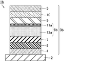
- FIG. 3 is a schematic cross-sectional view showing the organic EL display panel of Example 2.
- the organic EL display panel 1 b includes a substrate 2 and an organic EL element 3 b disposed on the substrate 2.
- the organic EL element 3b has an anode 4, a hole injection layer 6, a hole transport layer 7, a light emitting layer 8b, an electron transport layer 9, an electron injection layer 10, and a cathode 5 in this order from the substrate 2 side.
- the light emitting layer 8b has a light emitting host layer 12a on the anode 4 side and a light emitting dopant layer 11a on the cathode 5 side.
- the luminescent host material constituting the luminescent host layer 12a phosphorescent material type 4,4′-N, N′-dicarbazole-biphenyl (CBP) having bipolar characteristics and high hole transport characteristics was used.
- CBP phosphorescent material type 4,4′-N, N′-dicarbazole-biphenyl
- a light emitting host material (hole transporting host) having high hole transport characteristics described in Patent Document 8 can be used, and 1,3-di ( And carbazole derivatives such as N-carbazolyl) benzene (mCP) and 4,4 ′, 4 ′′ -tris (N-carbazolyl) -triphenylamine (TCTA).
- the thickness of the light emitting host layer 12a is, for example, 30 nm.
- the light-emitting host material preferably has a bipolar characteristic that promotes the generation of excitons of the light-emitting dopant material and can transport both holes and electrons.
- the hole mobility mu h of the light emitting host material, the electron mobility and mu e from the viewpoint of further enhancing the luminous efficiency, it is preferable that 1 ⁇ h / ⁇ e.
- bipolar characteristics are lost, holes and electrons are less likely to move, resulting in an increase in driving voltage and a decrease in device life. Therefore, when ⁇ h / ⁇ e is 100 or more, these disadvantages May become larger than the increase in luminous efficiency.
- ⁇ h / ⁇ e is, 1 ⁇ h / ⁇ e ⁇ more preferably 100, 1 ⁇ h / ⁇ e ⁇ It is particularly preferably 10.
- ⁇ h / ⁇ e is less than 100, the increase in luminous efficiency is greater than these disadvantages.
- ⁇ h / ⁇ e is less than 10
- the thickness of a normal organic EL element is about several tens of nm, and the light emitting region is sufficiently close to the light emitting dopant layer 11a side, so that the light emission efficiency can be further improved.
- the hole injection / transport characteristics of the hole injection layer 6 and the hole transport layer 7 are preferably higher than the electron injection / transport characteristics of the electron injection layer 10 and the electron transport layer 9.
- the number of holes in the light emitting host layer 12a is preferably larger than the number of electrons.
- the organic EL element 3b of Example 2 can be driven on the following principle.
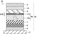
- FIG. 4 is an explanatory diagram for explaining the driving principle of the organic EL element in FIG.
- holes are injected from the anode 4 to the light emitting host layer 12a side of the light emitting dopant layer 11a through the hole injection layer 6, the hole transport layer 7, and the light emitting host layer 12a.
- electrons are injected from the cathode 5 through the electron injection layer 10 and the electron transport layer 9 to the light emitting host layer 12a side of the light emitting dopant layer 11a.
- the organic EL element 3b holes and electrons emit light by recombination near the interface between the light emitting dopant layer and the light emitting host layer (on the light emitting host layer 12a side of the light emitting dopant layer 11a).
- the light emitting region ER2 is limited to a narrow region near the interface between the light emitting dopant layer 11a and the light emitting host layer 12a and the density of excitons is increased, the luminous efficiency is sufficiently increased as in the first embodiment. be able to.
- the manufacturing efficiency can be improved as in the first embodiment.
- the organic EL element 3b may appropriately include a hole blocking layer and an electron blocking layer in addition to the configuration of Example 2, or a positive electrode in which the hole injection layer 6 and the hole transport layer 7 are integrated.
- a layer having two or more functions such as a hole injection layer / hole transport layer or an electron injection layer / electron transport layer in which the electron transport layer 9 and the electron injection layer 10 are integrated may be included.
- Example 2 Even in the case of a bottom emission type organic EL display panel that emits light from the cathode 5 side in a configuration in which 12a, a hole transport layer 7, a hole injection layer 6, and an anode 4 are arranged, Example 2 It is clear that the same effect is achieved.
- Example 3 relates to an organic EL element including an anode, a light emitting layer, and a cathode in order from the substrate side, and a top emission type organic EL display panel including the organic EL element, and the light emitting layer is disposed on the anode side.
- the present invention relates to a structure having a light emitting dopant layer and a light emitting host layer on the cathode side.
- a doped electron transport layer composed of a material in which an n-type impurity is doped in a substance having electron transport properties is disposed between the light emitting host layer and the cathode.
- the organic EL element of Example 3 is the same as the organic EL element of Example 1 except that the doped electron transport layer is disposed instead of the electron transport layer and the electron injection layer is not disposed. Description is omitted.
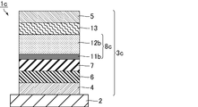
- FIG. 5 is a schematic cross-sectional view showing the organic EL display panel of Example 3.
- the organic EL display panel 1 c includes a substrate 2 and an organic EL element 3 c disposed on the substrate 2.
- the organic EL element 3 c includes an anode 4, a hole injection layer 6, a hole transport layer 7, a light emitting layer 8 c, a doped electron transport layer 13, and a cathode 5 in order from the substrate 2 side.
- the light emitting layer 8c has a light emitting dopant layer 11b on the anode 4 side and a light emitting host layer 12b on the cathode 5 side.
- the light emitting dopant layer 11b is the same as the light emitting dopant layer 11a of Example 1 except that the thickness is 1 nm.
- the light emitting host layer 12b is the same as the light emitting host layer 12a of Example 1 except that the thickness is 29 nm.
- the T1 level (2.5 eV) of the hole transport layer 7 is higher than the T1 level (2.0 eV) of the light-emitting dopant layer 11b.
- the doped electron transport layer 13 a material obtained by doping Bphen, which is a material constituting the electron transport layer, with cesium carbonate (Cs 2 CO 3 ) as an n-type impurity so that its concentration becomes 1% by weight is used.
- the thickness was 15 nm.
- the n-type impurity for example, an alkali metal oxide or carbonate, an alkaline earth metal oxide or carbonate, lithium oxide (Li 2 O), or barium carbonate (BaCo) can be used. 3 ) and the like, but an element having a large atomic weight is less susceptible to thermal diffusion and the like, and is more reliable, so BaCo 3 is more preferable.
- the light emitting layer 8c of the organic EL element of Example 3 has the same configuration as the light emitting layer 8a of the organic EL element of Example 1, the light emitting region is narrow near the interface between the light emitting dopant layer 11b and the light emitting host layer 12b. It is clear that the luminous efficiency is sufficiently increased when limited to a region.
- the manufacturing efficiency can be improved as in the first embodiment.
- the first additional effect will be described.
- the work function of ITO or IZO (about ⁇ 5 eV). If there is a large difference between the LUMO level of the electron transport layer and the electron transport layer, there is a concern that the performance of injecting electrons into the electron transport layer will be reduced.
- the doped electron transport layer 13 is disposed between the light emitting host layer 12b and the cathode 5, and the doped electron transport layer 13 itself has a charge.
- the cathode 5 can be connected to the cathode 5 in an ohmic manner, and the above-described deterioration of the electron injection performance can be sufficiently prevented. Further, since the electron transport property of the doped electron transport layer 13 is high, if the LUMO level of the doped electron transport layer 13 is brought close to the LUMO level of the light emitting host layer 12b, electrons are more easily injected into the light emitting host layer 12b. be able to.
- the cathode 5 is formed (for example, during sputtering).
- the already formed layers for example, the electron transport layer 9) are damaged by secondary electrons, plasma, and the like emitted to the surface, and the functions of these layers are deteriorated.
- the doped electron transport layer 13 is disposed between the light emitting host layer 12b and the cathode 5, and the doped electron transport layer 13 itself has a charge.
- the thickness of the doped electron transport layer 13 is preferably 5 nm or more, and more preferably 10 nm or more. In addition, since transparency is maintained even if the thickness of the doped electron transport layer 13 is increased to about several hundred nm, there is no optical loss.
- the light emitting region ER3 is the light emitting layer 108b.
- a light emitting point also exists on the cathode 5 side of the light emitting layer 108b.
- the conventional organic EL display panel 101c when the doped electron transport layer 13 used in Example 3 is disposed on the light emitting layer 108b, excitons generated on the cathode 5 side of the light emitting layer 108b are converted into the doped electron transport layer. Since it is quenched by 13, the light emission efficiency is lowered.
- the doped electron transport layer 13 used in Example 3 on the conventional organic EL display panel 101c, another buffer layer (between the light emitting layer 108b and the doped electron transport layer 13 (for example, it is necessary to further dispose an electron transport layer), but in this case, the production efficiency is lowered.
- the light emitting host layer 12b is disposed between the light emitting dopant layer 11b and the doped electron transport layer 13, and between the light emitting dopant layer 11b and the doped electron transport layer 13. Therefore, excitons are not quenched by the doped electron transport layer 13.
- Comparative Example 1 relates to an organic EL element including an anode, a light-emitting layer, and a cathode in order from the substrate side, and an organic EL display panel including the organic EL element.
- the light-emitting layer includes a light-emitting dopant material and a light-emitting host material. It is related with the structure which is a mixed mixed layer. Since the organic EL element of Comparative Example 1 is the same as the organic EL element of Example 3 except for the configuration of the light emitting layer, the description of overlapping points is omitted.
- FIG. 6 is a schematic cross-sectional view showing an organic EL display panel of Comparative Example 1.
- the organic EL display panel 101 a includes a substrate 2 and an organic EL element 103 a disposed on the substrate 2.
- the organic EL element 103a has an anode 4, a hole injection layer 6, a hole transport layer 7, a light emitting layer 108a, a doped electron transport layer 13, and a cathode 5 in this order from the substrate 2 side.
- the light emitting layer 108a is a mixed layer 114a in which a light emitting dopant material and a light emitting host material are mixed.
- the mixed layer 114a a layer obtained by co-evaporating Ir (ppy) 3, which is a light emitting dopant material, and CBP, which is a light emitting host material, at a weight ratio of 90:10 was used, and the thickness thereof was set to 30 nm.
- Comparative Example 2 relates to an organic EL element including an anode, a light emitting layer, and a cathode in order from the substrate side, and an organic EL display panel including the organic EL element.
- the light emitting layer includes a light emitting dopant material and a light emitting host material. It is related with the structure which is a mixed mixed layer.
- the organic EL device of Comparative Example 2 is the same as that of Example 3 except that the configuration of the light emitting layer, the configuration of the cathode, and an element in which an electron transport layer and an electron injection layer are sequentially stacked instead of the doped electron transport layer are arranged. Since it is the same as that of the organic EL element, description is abbreviate
- FIG. 7 is a schematic cross-sectional view showing an organic EL display panel of Comparative Example 2.
- the organic EL display panel 101 b includes a substrate 2 and an organic EL element 103 b disposed on the substrate 2.
- the organic EL element 103b includes an anode 4, a hole injection layer 6, a hole transport layer 7, a light emitting layer 108a, an electron transport layer 9, an electron injection layer 10, and a cathode 105 in this order from the substrate 2 side.
- the light emitting layer 108a is a mixed layer 114a in which a light emitting dopant material and a light emitting host material are mixed.
- the cathode 105 includes a metal layer 15a and a transparent conductive layer 18 in order from the substrate 2 side.
- Bphen was used as the electron transport layer 9 and its thickness was set to 15 nm.
- lithium fluoride LiF was used, and the thickness was set to 0.5 nm.
- an alloy of magnesium (Mg) and silver (Ag) (hereinafter also referred to as “Mg—Ag”) was used, and the thickness thereof was 1 nm.
- Mg—Ag an alloy of magnesium (Mg) and silver (Ag)
- ITO transparent conductive layer 18 constituting the cathode 105
- its thickness was 100 nm.
- Luminous efficiency was evaluated at a luminance of 1000 cd / m 2 using an FPD module inspection device (MD series) manufactured by Otsuka Electronics Co., Ltd. equipped with a color luminance meter (BM-5A) manufactured by Topcon as a detector.
- MD series FPD module inspection device
- BM-5A color luminance meter
- the luminous efficiency of the organic EL element of Comparative Example 1 was reduced by 20% compared with the luminous efficiency of the organic EL element of Example 3. This is because the light-emitting layer 108a of the organic EL element of Comparative Example 1 has a configuration in which a light-emitting dopant material and a light-emitting host material are mixed, so that the light-emitting region is expanded and as a result, the light emission efficiency is lowered. Conceivable. Furthermore, in the organic EL element of Comparative Example 1, since the doped electron transport layer 13 is disposed on the light emitting layer 108 a, excitons generated on the doped electron transport layer 13 side of the light emitting layer 108 a are caused by the doped electron transport layer 13. It is thought that this is because the emission efficiency was lowered as a result of being quenched.
- the organic EL device of Comparative Example 2 did not emit light. This is because Mg—Ag (metal layer 15a), which has been thinned to emit light from the cathode 105 side, is damaged when ITO (transparent conductive layer 18) is formed, and the influence of this is due to electron injection. It is thought that this is because the layer 10 and the electron transport layer 9 have been reached.
- Mg—Ag metal layer 15a
- ITO transparent conductive layer 18
- the organic EL element of Example 3 has the light emitting layer 8c in which the light emitting dopant material and the light emitting host material are contained in different layers and the doped electron transport layer 13 is arranged, the light emission efficiency Can be sufficiently increased, and damage in forming the cathode 5 can be sufficiently prevented.
- Example 4 relates to an organic EL element including an anode, a light emitting layer, and a cathode in order from the substrate side, and a top emission type organic EL display panel including the organic EL element, and the light emitting layer is disposed on the anode side.
- the present invention relates to a structure having a light emitting dopant layer and a light emitting host layer on the cathode side.
- the light emitting host layer is composed of two kinds of light emitting host materials. Since the organic EL element of Example 4 is the same as the organic EL element of Example 3 except for the configuration of the light-emitting host layer, description of overlapping points is omitted.
- FIG. 8 is a schematic cross-sectional view showing an organic EL display panel of Example 4.
- the organic EL display panel 1 d includes a substrate 2 and an organic EL element 3 d disposed on the substrate 2.
- the organic EL element 3d has an anode 4, a hole injection layer 6, a hole transport layer 7, a light emitting layer 8d, a doped electron transport layer 13, and a cathode 5 in this order from the substrate 2 side.
- the light emitting layer 8d has a light emitting dopant layer 11b on the anode 4 side and a light emitting host layer 12c on the cathode 5 side.
- the light emitting host layer 12c is composed of two kinds of light emitting dopant materials.
- the light-emitting host layer 12c As the light-emitting host layer 12c, a mixture of TPBI having bipolar characteristics and high electron transport characteristics and CBP having hole transport characteristics in a weight ratio of 80:20 was used, and the thickness was 29 nm.
- the light emitting host layer 12c does not substantially contain a light emitting dopant material.
- the light emitting layer 8d of the organic EL element of Example 4 has the same configuration as the light emitting layer 8c of the organic EL element of Example 3 except for the structure of the light emitting host layer, the light emitting region has a light emitting dopant layer 11b and a light emitting host layer. It is obvious that the light emission efficiency is sufficiently increased by being limited to a narrow region near the interface with 12c.
- the manufacturing efficiency can be improved as in the third embodiment.
- Example 4 since the doped electron transport layer 13 is disposed in the organic EL display panel of Example 4, the additional effect of Example 3 can be achieved.
- the light-emitting host material A When a material having bipolar characteristics and high electron transport properties (hereinafter also referred to as “light-emitting host material A”) like the light-emitting host material used in Example 3 is used, the light-emitting host material A is used.
- the number of electrons in the light emitting host layer is larger than the number of holes, and the electrons can be transported to the light emitting dopant layer.
- the light emitting host material A may have low resistance to holes. When holes are injected excessively, holes that could not be used for light emission in the light emitting doping layer flow into the light emitting host layer and stay in the light emitting host layer, thus degrading the light emitting host material A. I might let you.
- the material stays in the light-emitting host layer.
- the released holes can be released from the light emitting host material A, and deterioration of the light emitting host material A can be sufficiently prevented.
- the LUMO level of the light emitting host material B is preferably higher than the LUMO level of the light emitting host material A.
- the HOMO level of the light emitting host material B is preferably higher than the HOMO level of the light emitting host material A.
- Example 5 relates to an organic EL element including an anode, a light emitting layer, and a cathode in order from the substrate side, and a top emission type organic EL display panel including the organic EL element, and the light emitting layer is disposed on the anode side.
- the present invention relates to a structure having a light emitting dopant layer and a light emitting host layer on the cathode side.
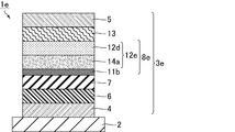
- the light-emitting host layer includes a mixed layer in which a light-emitting dopant material is mixed in part from the anode side and a light-emitting host layer that does not contain a light-emitting dopant material. Since the organic EL element of Example 5 is the same as the organic EL element of Example 3 except for the configuration of the light emitting layer, the description of overlapping points is omitted.
- FIG. 9 is a schematic cross-sectional view showing an organic EL display panel of Example 5.
- the organic EL display panel 1 e includes a substrate 2 and an organic EL element 3 e disposed on the substrate 2.
- the organic EL element 3e includes an anode 4, a hole injection layer 6, a hole transport layer 7, a light emitting layer 8e, a doped electron transport layer 13, and a cathode 5 in this order from the substrate 2 side.
- the light emitting layer 8e has a light emitting dopant layer 11b on the anode 4 side and a light emitting host layer 12e on the cathode 5 side.
- the light emitting host layer 12e includes, in order from the anode 4 side, a mixed layer 14a in which a light emitting dopant material and a light emitting host material are mixed, and a light emitting host layer 12d that does not contain a light emitting dopant material.
- the light emitting host layer 12d is the same as the light emitting host layer 12b of Example 3 except that the film thickness is 19 nm.
- a diamine pyrene-based blue delayed fluorescent material that is a light-emitting dopant material and a fluorescent material-based BH-232 manufactured by Idemitsu Kosan Co., Ltd. are co-deposited at a weight ratio of 5:95. The thickness was 10 nm.
- the light emitting host layer which is the light emitting host material constituting the light emitting host layer.
- the light emitting host layer itself generates excitons.
- the excitons generated in the light emitting host layer emit light by moving to the light emitting dopant layer with energy, but a part of it is diffused and the light emitting host material emits light or is deactivated. As a result, color mixing may occur and light emission efficiency may be reduced.
- the exciton generated in the light emitting host layer is also obtained by mixing the light emitting dopant material into a part of the light emitting host layer, that is, by further arranging the mixed layer 14a in which the light emitting dopant material and the light emitting host material are mixed. Since it can be used for light emission, the light emission efficiency can be further increased. In addition, since the deterioration of the light emitting host material can be sufficiently prevented, the element life of the organic EL element can be extended.
- the concentration of the light emitting dopant material in the mixed layer 14a is as follows from the viewpoint of further increasing the light emission efficiency.
- the height is preferably increased from the light emitting host layer 12d side to the light emitting dopant layer 11b side.
- the manufacturing efficiency can be improved as in the third embodiment.
- Example 5 since the doped electron transport layer 13 is disposed in the organic EL display panel of Example 5, the additional effect of Example 3 can be achieved.
- Example 6 relates to an organic EL element including an anode, a light emitting layer, and a cathode in order from the substrate side, and a top emission type organic EL display panel including the organic EL element, and the light emitting layer is disposed on the anode side.
- the present invention relates to a structure having a light emitting dopant layer and a light emitting host layer on the cathode side.
- the light-emitting host layer includes a mixed layer in which a light-emitting dopant material is mixed in part from the anode side and a light-emitting host layer that does not contain a light-emitting dopant material. Since the organic EL element of Example 6 is the same as the organic EL element of Example 5 except for the configuration of the light emitting layer, the description of overlapping points is omitted.
- FIG. 10 is a schematic cross-sectional view showing the organic EL display panel of Example 6.
- the organic EL display panel 1 f includes a substrate 2 and an organic EL element 3 f disposed on the substrate 2.
- the organic EL element 3f includes an anode 4, a hole injection layer 6, a hole transport layer 7, a light emitting layer 8f, a doped electron transport layer 13, and a cathode 5 in this order from the substrate 2 side.
- the light emitting layer 8f has a light emitting dopant layer 11b on the anode 4 side and a light emitting host layer 12f on the cathode 5 side.
- the light emitting host layer 12f includes, in order from the anode 4 side, a mixed layer 14b in which a light emitting dopant material and a light emitting host material are mixed, and a light emitting host layer 12d that does not contain a light emitting dopant material.
- the mixed layer 14b a diamine pyrene-based blue delayed fluorescent material that is a light-emitting dopant material and a fluorescent material-based BH-232 manufactured by Idemitsu Kosan Co., Ltd. are used, and the thickness thereof is 10 nm. It was.
- the concentration of the light emitting dopant material in the mixed layer 14b is from the light emitting host layer 12d side to the light emitting dopant layer 11b side so that the light emitting host layer 12d side is 0% by weight and the light emitting dopant layer 11b side is 100% by weight. It set so that it might become continuously high.
- the state in which the concentration of the light-emitting dopant material in the mixed layer 14b changes can be realized by using a gradient deposition method.
- the organic EL device of Example 6 is the same as the organic EL device of Example 5 except for the configuration of the light emitting layer, and Example 5 is also provided in that a mixed layer in which a light emitting dopant material and a light emitting host material are mixed is further arranged. Therefore, it is clear that the same effects as those of the fifth embodiment are obtained.
- Example 7 relates to an organic EL element including an anode, a light emitting layer, and a cathode in order from the substrate side, and a top emission type organic EL display panel including the organic EL element, and the light emitting layer is disposed on the anode side.
- the present invention relates to a structure having a light emitting dopant layer and a light emitting host layer on the cathode side.
- an electron transport layer, a metal layer, and a p-type oxide layer are sequentially disposed between the light emitting host layer and the cathode.
- the organic EL element of Example 7 is the organic EL element of Example 3 except that instead of the doped electron transport layer, an electron transport layer, a metal layer, and a p-type oxide layer are sequentially stacked. Since it is the same as an element, description is abbreviate
- FIG. 11 is a schematic cross-sectional view showing an organic EL display panel of Example 7.
- the organic EL display panel 1 g includes a substrate 2 and an organic EL element 3 g disposed on the substrate 2.
- the organic EL element 3g includes, in order from the substrate 2, the anode 4, the hole injection layer 6, the hole transport layer 7, the light emitting layer 8c, the electron transport layer 9, the metal layer 15b, the p-type oxide layer 16, and A cathode 5 is provided.
- the electron transport layer 9 Bphen was used and its thickness was set to 15 nm. In addition, as the electron transport layer 9, what a normal organic EL element has can be used.
- Li As the metal layer 15b, Li was used and its thickness was 1 nm. Li was deposited using an alkaline dispenser. In addition, calcium (Ca) or the like can be used as the metal layer 15b.
- MoO 3 As the p-type oxide layer 16, MoO 3 was used and the thickness thereof was 15 nm. In addition, as the p-type oxide layer 16, vanadium pentoxide (V 2 O 5 ) or the like can be used.
- the organic EL element of Example 7 sufficiently increases the light emission efficiency and the production efficiency. Can be made excellent.
- FIG. 12 is a band correlation diagram on the cathode side of the organic EL display panel of Example 7. As shown in FIG. 12, the p-type oxide layer 16 (MoO 3 , work function: ⁇ 5.8 eV) functions as a charge generation layer, and the cathode 5 (ITO, work function: ⁇ 5.0 eV) starts to generate holes. Can be injected into the metal layer 15b (Li).
- the LUMO level of the material constituting the electron transport layer 9 is ⁇ 3.05 eV, which is lower than the work function ⁇ 2.9 eV of the metal layer 15 b (Li). Therefore, electrons can be injected from the metal layer 15b (Li) into the electron transport layer 9 without a barrier.
- MoO 3 is an inorganic oxide, depending on the material constituting the doped electron transport layer as already described in Example 3, it is necessary to form the cathode 5 (ITO) on the doped electron transport layer 13.
- the damage may be larger than the damage when the cathode 5 (ITO) is formed on the p-type oxide layer 16 (MoO 3 ).
- damage during formation of the cathode 5 (ITO) can be sufficiently prevented without doping the material constituting the electron transport layer with a dopant. Can be injected from the cathode 5 (ITO) to the electron transport layer 9 side without a barrier.
- the dopant itself constituting the doped electron transport layer 13 has high activity and high reactivity, even if the doping amount is increased, the remaining active material may be damaged when the cathode 5 (ITO) is formed. .
- the p-type oxide layer 16 (MoO 3 ) has low activity, it is hardly damaged when the cathode 5 (ITO) is formed.
- the effect of disposing the doped electron transport layer may not be obtained. Therefore, the use of the structure of Example 7 increases the choice of materials constituting the organic EL element. Further, the production efficiency can be further improved.
- Example 8 relates to an organic EL element including an anode, a light emitting layer, and a cathode in order from the substrate side, and a top emission type organic EL display panel including the organic EL element, and the light emitting layer is disposed on the anode side.
- the present invention relates to a structure having a light emitting dopant layer and a light emitting host layer on the cathode side.
- an electron transport layer, a metal layer, and a p-type doped layer composed of a material doped with a p-type dopant are sequentially arranged between the light emitting host layer and the cathode. Since the organic EL element of Example 8 is the same as the organic EL element of Example 7 except that a p-type doped layer is disposed instead of the p-type oxide layer, the description of overlapping points is omitted. To do.
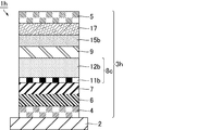
- FIG. 13 is a schematic cross-sectional view showing an organic EL display panel of Example 8.
- the organic EL display panel 1 h includes a substrate 2 and an organic EL element 3 h disposed on the substrate 2.
- the organic EL element 3h includes an anode 4, a hole injection layer 6, a hole transport layer 7, a light emitting layer 8c, an electron transport layer 9, a metal layer 15b, a p-type doped layer 17, and a cathode 5 in this order from the substrate 2 side. have.
- a layer in which MoO 3 (p-type dopant) and ⁇ -NPD which is a material constituting the hole transport layer are co-deposited at a weight ratio of 20:80 is used, and the thickness is 15 nm. did.
- the organic EL element of Example 8 Since the light emitting layer 8c of the organic EL element of Example 8 has the same configuration as that of the light emitting layer 8c of the organic EL element of Example 3, the organic EL element of Example 8 sufficiently increases the light emission efficiency and the production efficiency. Can be made excellent.
- FIG. 14 is a band correlation diagram on the cathode side of the organic EL display panel of Example 8. As shown in FIG.
- the p-type doped layer 17 functions as a charge generation layer, and when holes are injected from the cathode 5 (ITO, work function: ⁇ 5.0 eV). Electrons can be injected into the metal layer 15b (Li). Thus, electric charges can be transported smoothly from the cathode 5 (ITO) to the metal layer 15b (Li).
- the LUMO level of the material constituting the electron transport layer 9 is ⁇ 3.05 eV, which is lower than the work function ⁇ 2.9 eV of the metal layer 15 b (Li). Therefore, electrons can be injected from the metal layer 15b (Li) into the electron transport layer 9 without a barrier.
- the damage received when forming the cathode 5 (ITO) is small. Further, depending on the material constituting the doped electron transport layer as already described in Example 3, the damage when forming the cathode 5 (ITO) on the doped electron transport layer 13 may cause damage to the cathode on the p-type doped layer 17. 5 (ITO) may be larger than the damage when forming. In such a case, by using the configuration as in Example 8, damage during the formation of the cathode 5 (ITO) can be sufficiently prevented without doping the material constituting the electron transport layer with the dopant. Can be injected from the cathode 5 (ITO) to the electron transport layer 9 side without a barrier.
- a low activity material MoO 3
- the p-type doped layer 17 has low activity, it is hardly damaged when the cathode 5 (ITO) is formed.
- the effect of disposing the doped electron transport layer may not be obtained. Therefore, the use of the structure of Example 8 increases the choice of materials constituting the organic EL element. Further, the production efficiency can be further improved.
- a p-type oxide layer such as MoO 3 as used in Example 7 is disposed between the metal layer 15b and the p-type doped layer 17 in the same manner. Can produce various effects.
- Example 9 relates to an organic EL element including an anode, a light emitting layer, and a cathode in order from the substrate side, and a top emission type organic EL display panel including the organic EL element, and the light emitting layer is disposed on the anode side.
- the present invention relates to a structure having a light emitting dopant layer and a light emitting host layer on the cathode side. Further, a doped electron transport layer as already described in Example 3 is disposed between the light emitting host layer and the cathode, and the cathode has a metal layer and a transparent conductive layer in this order from the substrate side. Since the organic EL element of Example 9 is the same as the organic EL element of Example 3 except for the configuration of the cathode, the description of overlapping points is omitted.
- FIG. 15 is a schematic cross-sectional view showing an organic EL display panel of Example 9.
- the organic EL display panel 1 i includes a substrate 2 and an organic EL element 3 i disposed on the substrate 2.
- the organic EL element 3i includes an anode 4, a hole injection layer 6, a hole transport layer 7, a light emitting layer 8c, a doped electron transport layer 13, and a cathode 5a in this order from the substrate 2 side.
- the cathode 5a includes a metal layer 15c and a transparent conductive layer 18 in order from the substrate 2 side.
- the metal layer 15c which comprises the cathode 5a Ag was used and the thickness was 19 nm.
- a general metal can be used as the metal layer 15c.
- ITO transparent conductive layer 18 constituting the cathode 5a
- its thickness was 100 nm.
- the organic EL element of Example 9 sufficiently increases the light emission efficiency and the production efficiency. Can be made excellent.
- Ag has light translucency, but can enhance the interference effect, so that the front luminance can be increased.
- the metal layer 15c (Ag) it is possible to further prevent damage to the doped electron transport layer 13 when the cathode 5 (ITO) is formed.
- the light emitting layer may have the light emitting dopant layer on the anode side and the light emitting host layer on the cathode side. Accordingly, the light emitting dopant layer and the light emitting host layer can be effectively utilized in accordance with the charge transport property of the light emitting host material.
- the light emitting host material has bipolar characteristics, and the hole mobility of the light emitting host material may be smaller than the electron mobility.
- the hole mobility and electron mobility of the light emitting host material are about 10 ⁇ 7 to 10 ⁇ 4 m 2 / (V ⁇ s), and the hole mobility is about 1/10 smaller than the electron mobility. Is preferred. Thereby, according to arrangement
- the light emitting layer may have the light emitting host layer on the anode side and the light emitting dopant layer on the cathode side. Accordingly, the light emitting dopant layer and the light emitting host layer can be effectively utilized in accordance with the charge transport property of the light emitting host material.
- the light emitting host material has bipolar characteristics, and the hole mobility of the light emitting host material may be larger than the electron mobility.
- the hole mobility and electron mobility of the light emitting host material are about 10 ⁇ 7 to 10 ⁇ 4 m 2 / (V ⁇ s), and the hole mobility is about 10 times larger than the electron mobility. preferable. Thereby, according to arrangement
- the light emitting dopant layer may have a thickness of 5 nm or less. Thereby, the density of excitons can be further increased, and the luminous efficiency can be further increased. Further, by reducing the thickness of the light-emitting dopant layer, the amount of the light-emitting dopant material used can be suppressed, so that the production efficiency is further improved and the occurrence of color mixing between adjacent pixels is sufficiently achieved. Can be prevented.
- the concentration of the light emitting dopant material in the light emitting dopant layer may be 90% by weight or more.
- the organic electroluminescence display panel is a top emission type that emits light from the cathode side, and the organic electroluminescence element is, in order from the substrate side, the anode, the hole transport layer, the light emitting dopant layer, and the
- the doped host transport layer may include a light emitting host layer, a doped electron transport layer, and the cathode, and the doped electron transport layer may be composed of a material doped with a dopant in a substance having electron transport characteristics. This makes it possible to sufficiently prevent the electron injection performance from the cathode from being lowered by utilizing the fact that the doped electron transport layer itself has a charge. In addition, by disposing the doped electron transport layer, it is possible to sufficiently prevent damage at the time of forming the cathode with respect to each layer already formed before the cathode.
- the dopant may be an n-type impurity. Thereby, electrons can be suitably transported by the doped electron transport layer.
- the energy level of the lowest triplet state of the material constituting the hole transport layer may be higher than the energy level of the lowest triplet state of the light-emitting dopant material. Thereby, holes can be transported from the hole transport layer to the light emitting dopant layer without a barrier.
- the minimum value among the energy levels of the lowest triplet state of the material constituting the hole transport layer is It is preferably higher than the maximum value among the energy levels of the lowest triplet state of the luminescent dopant material.
- the light emitting host layer may contain at least two types of light emitting host materials.
- the at least two kinds of light-emitting host materials may include a material having an electron transport property and a material having a hole transport property. Accordingly, the light emitting host layer can be effectively utilized by utilizing the effect of sufficiently preventing the material having the electron transport property from being deteriorated by the material having the hole transport property.
- the highest occupied orbital level of the material having the hole transport property may be higher than the highest occupied orbital level of the material having the electron transport property. Accordingly, the light emitting host layer can be effectively utilized by utilizing the effect of making it difficult for electrons to move toward the material having the hole transporting property.
- the minimum value among the highest occupied orbital levels of the material having the hole transport property is the electron. It is preferably higher than the maximum value among the highest occupied orbital levels of materials having transport properties.
- the lowest vacant orbital level of the material having the hole transporting property may be higher than the lowest vacant orbital level of the material having the electron transporting property.
- the light emitting host layer can be effectively used by utilizing the effect of facilitating the movement of holes toward the material having the hole transport property.
- the minimum value among the lowest vacant orbital levels of the material having the hole transport property is the electron transport property. It is preferable that it is higher than the maximum value among the lowest unoccupied orbital levels of the material having characteristics.
- the light emitting host layer may have a mixed layer on the anode side, and the mixed layer may be a layer in which a light emitting dopant material and a light emitting host material are mixed.
- the concentration of the light emitting dopant material in the mixed layer may increase from the cathode side to the anode side.
- excitons generated in the light emitting host layer excitons distributed near the interface between the light emitting dopant layer and the mixed layer can be efficiently used for light emission. Efficiency can be further increased.
- the element life of the organic EL element can be extended.
- the organic electroluminescence display panel is a top emission type that emits light from the cathode side
- the organic electroluminescence element is, in order from the substrate side, the anode, the hole transport layer, the light emitting dopant layer, and the A light emitting host layer, an electron transport layer, a metal layer, a p-type oxide layer, and the cathode may be included.
- an electron transport layer, a metal layer, a p-type oxide layer, and the cathode may be included.
- electrons can be transported from the cathode to the electron transport layer side without any barrier.
- the p-type oxide layer it is possible to sufficiently prevent damage when the cathode is formed on each layer already formed before the cathode.
- the organic electroluminescence display panel is a top emission type that emits light from the cathode side
- the organic electroluminescence element is, in order from the substrate side, the anode, the hole transport layer, the light emitting dopant layer, and the
- the light emitting host layer, the electron transport layer, the metal layer, the p-type doped layer, and the cathode may be included, and the p-type doped layer may be made of a material doped with a p-type dopant.
- the p-type doped layer may be made of a material doped with a p-type dopant.
- the p-type doped layer may be composed of a material in which a substance having a hole transport property is doped with the p-type dopant. Accordingly, the p-type doped layer can be effectively utilized by utilizing the effect that a sufficient amount of electric charge exists in the p-type doped layer.
- the work function of the metal layer may be higher than the lowest unoccupied orbital level of the material constituting the electron transport layer. Thereby, electrons can be transported from the metal layer to the electron transport layer without a barrier.
- the work function of the said metal layer is higher than the maximum value in the lowest empty orbital level of the material which comprises the said electron carrying layer.
- the cathode may have a metal layer and a transparent conductive layer in order from the substrate side. Thereby, the damage at the time of forming the said cathode can fully be prevented with respect to each layer already formed before the said cathode.
- Organic EL display panel 2 Substrate 3a, 3b, 3c, 3d, 3e, 3f, 3g, 3h, 3i, 103a 103b, 103c: Organic EL element 4: Anode 5, 5a, 105: Cathode 6: Hole injection layer 7: Hole transport layer 8a, 8b, 8c, 8d, 8e, 8f, 108a, 108b: Light emitting layer 9: Electron transport layer 10: electron injection layer 11a, 11b: light emitting dopant layers 12a, 12b, 12c, 12d, 12e, 12f: light emitting host layer 13: doped electron transport layers 14a, 14b, 114a: mixed layers 15a, 15b, 15c: Metal layer 16: p-type oxide layer 17: p-type doped layer 18: transparent conductive layer 19: light-emitting do
Landscapes
- Physics & Mathematics (AREA)
- Optics & Photonics (AREA)
- Electroluminescent Light Sources (AREA)
Abstract
本発明は、発光効率を充分に高め、製造効率を優れたものとすることができる有機エレクトロルミネッセンス素子と、上記有機エレクトロルミネッセンス素子を備える有機エレクトロルミネッセンス表示パネルとを提供する。本発明の有機エレクトロルミネッセンス素子は、陽極と、発光層と、陰極とを順に備える有機エレクトロルミネッセンス素子であって、上記発光層は、発光ドーパント層及び発光ホスト層を有し、上記発光ドーパント層は、発光ドーパント材料を含有し、発光ホスト材料を実質的に含有せず、上記発光ホスト層は、発光ホスト材料を含有し、発光ドーパント材料を実質的に含有しないものである。
Description
本発明は、有機エレクトロルミネッセンス素子(以下、「有機EL素子」とも言う。)、及び、有機エレクトロルミネッセンス表示パネル(以下、「有機EL表示パネル」とも言う。)に関する。より詳しくは、発光効率の高い有機EL素子、及び、上記有機EL素子を備える有機EL表示パネルに関するものである。
近年、薄型表示装置に用いられる表示素子として、有機材料の電界発光を利用した有機EL素子が注目されている。有機EL素子は、陽極から注入された正孔と陰極から注入された電子とが両電極間に配置された発光層内で再結合することによって発光するものである。このような自発光型の有機EL素子は、高輝度発光、高速応答、広視野角、薄型軽量等の優れた特徴を有しており、表示パネルや照明等の様々な分野に応用されることが期待されている。
有機EL素子の発光層としては、通常、発光を主に担う発光ドーパント材料と、正孔及び電子の輸送を主に担う発光ホスト材料とが共蒸着により混合された層が用いられている。このような構成に対して、有機EL素子を更に高機能化させることが検討されており、例えば、以下が挙げられる。
上述したような通常の発光層の他に、発光ドーパント材料の濃度が100重量%である層が配置された有機EL素子が知られている(例えば、特許文献1参照)。
通常の発光層の他に、発光ホスト材料を主成分として発光ドーパント材料を含まない層が配置された有機EL素子が知られている(例えば、特許文献2参照)。
通常の発光層の代わりに、再結合中心として働いて発光する蛍光性有機化合物からなり、平均膜厚が蛍光性有機化合物の単分子膜の膜厚よりも薄い島状薄膜が配置された有機EL素子が知られている(例えば、特許文献3参照)。
通常の発光層の他に、陽極及び陰極間に配置された有機化合物層と陰極との間に、金属又は金属塩でドーピングした金属ドーピング層が配置された有機EL素子が知られている(例えば、特許文献4、5参照)。
通常の発光層を構成する材料の特性を所定のものとし、所定の特性を有する障壁層が配置された有機EL素子が知られている(例えば、特許文献6参照)。また、通常の発光層を構成する材料の特性を所定のものとして複数積層させた有機EL素子が知られている(例えば、特許文献7、8参照)。
通常の発光層の他に、効率増強層が配置された有機EL素子が知られている(例えば、非特許文献1、2参照)。
アラカネ等(T.Arakane,et al)、「新しいディープブルー蛍光材料と高性能化への応用(New Deep Blue Fluorescent Materials and Their Application to High Performance)」、IDW’11、2011、p.799-802
カワムラ等(M.Kawamura,et al)、「効率増強層を伴う高効率蛍光の青色有機発光ダイオード(Highly Efficient Fluorescent Blue OLEDs with Efficiency-enhancement Layer)」、SID10 DIGEST、2010、p.560-563
有機EL素子において、発光ホスト材料及び発光ドーパント材料が混合された発光層を用いると、発光領域が広がり、発光効率が低下することがあった。特に、青色蛍光材料で遅延蛍光させる場合、三重項-三重項融合(TTF:Triplet-Triplet Fusion)現象が発生しにくく、発光効率が高まらないことがあった。この理由について、以下に説明する。
図16は、従来の有機EL表示パネルを示す断面模式図である。図16に示すように、有機EL表示パネル101cは、基板2と、基板2上に配置された有機EL素子103cとを有している。有機EL素子103cは、基板2側から順に、陽極4、正孔輸送層7、発光層108b、電子輸送層9、及び、陰極5を有している。発光層108bは、発光ドーパント材料19、及び、発光ホスト材料20が共蒸着により混合された構成を有している。この場合、発光ドーパント材料19は発光層108b全体に分散されているため、図16に示すように、有機EL素子103cの発光領域ER3は発光層108b全体に広がっている。
高効率な発光を実現するためには、発光層内で生成される励起子の領域を狭い領域に限定し、励起子の密度を増加させることが考えられる。特に、青色蛍光材料で遅延蛍光させる場合は、TTF現象が発生しやすいように励起子の密度を増加させることが重要である。
しかしながら、図16に示すような有機EL素子103cにおいては、発光領域ER3が発光層108b全体に広がっているため、励起子の密度が減少し、発光効率が低下することがあった。特に、青色蛍光材料で遅延蛍光を利用する場合は、TTF現象が発生しにくくなり、発光効率が低下することがあった。
また、発光領域ER3が発光層108b全体に広がることによって、励起子が発光層108bに隣接する層(例えば、正孔輸送層7、電子輸送層9)に流出してしまうことが考えられる。この現象は、発光層108bに隣接する層の最低三重項状態のエネルギー準位(以下、「T1準位」とも言う。)が、発光層108bを構成する材料のT1準位よりも低いと生じてしまう。このため、発光層108bに隣接する層の種類が限定されるだけでなく、励起子の流出を防止するための層を更に配置することが必要になり、その結果、有機EL素子の構造が複雑し、製造効率が低下することがあった。
更に、発光層108bは、発光ドーパント材料19、及び、発光ホスト材料20を共蒸着することにより形成されるため、各材料の所望の重量比を実現するように蒸着速度を制御することが困難であり、製造効率が低下することがあった。
以上より、従来の有機EL素子103cは、発光効率を充分に高め、製造効率を優れたものとする点において工夫の余地があった。
上記特許文献1は、駆動電圧が低く、発光効率が高い有機EL素子を提供すると開示している。しかしながら、上記特許文献1に記載の発明は、上記特許文献1の図1に示されたように、発光ドーパント材料及び発光ホスト材料が混合された発光層を有しているため、発光効率を充分に高める点において工夫の余地があった。また、このような発光層は、発光ドーパント材料及び発光ホスト材料を共蒸着することにより形成されるため、製造効率を優れたものとする点において工夫の余地があった。
上記特許文献2は、耐久性を損なうことなく低電圧の駆動が可能な有機EL素子を提供すると開示している。しかしながら、上記特許文献2に記載の発明は、上記特許文献2の図1に示されたように、発光ドーパント材料及び発光ホスト材料が混合された発光層を有しているため、発光効率を充分に高める点において工夫の余地があった。また、このような発光層は、発光ドーパント材料及び発光ホスト材料を共蒸着することにより形成されるため、製造効率を優れたものとする点において工夫の余地があった。
上記特許文献3は、新たな層構成を有し、蛍光性有機化合物を有効に活用することが可能な有機EL素子を提供すると開示している。しかしながら、上記特許文献3に記載の発明では、正孔輸送層と電子輸送層との間に発光を担う島状薄膜が配置されており、島状薄膜が分布していない領域では、正孔輸送層と電子輸送層とが直結してしまうため、正孔及び電子の再結合が島状薄膜内で発生せず、その結果、発光効率が低下してしまうことが考えられる。よって、上記特許文献3に記載の発明は、発光効率を充分に高める点において工夫の余地があった。
上記特許文献4は、駆動電圧が低く、高効率、高輝度発光素子の作製を可能とする有機EL素子を提供すると開示している。しかしながら、上記特許文献4に記載の発明は、上記特許文献4の図1に示されたように、発光ドーパント材料及び発光ホスト材料が混合された発光層を有しているため、発光効率を充分に高める点において工夫の余地があった。また、このような発光層は、発光ドーパント材料及び発光ホスト材料を共蒸着することにより形成されるため、製造効率を優れたものとする点において工夫の余地があった。
上記特許文献5は、駆動電圧を低下させるとともに、発光スペクトルの制御が可能な有機EL素子を提供すると開示している。しかしながら、上記特許文献5に記載の発明は、上記特許文献5の図1に示されたように、発光ドーパント材料及び発光ホスト材料が混合された発光層を有しているため、発光効率を充分に高める点において工夫の余地があった。また、このような発光層は、発光ドーパント材料及び発光ホスト材料を共蒸着することにより形成されるため、製造効率を優れたものとする点において工夫の余地があった。これは、上記特許文献7、8についても同様である。
上記特許文献6は、発光層内部においてTTF現象を効率的に引き起こし、従来の蛍光素子の限界値と言われていた内部量子効率25%を大きく超える高効率な有機EL素子を提供すると開示している。しかしながら、TTF現象は二つの励起子間で発生する現象であるため、発光ドーパント材料の濃度が低い場合は、TTF現象が発生しにくくなると考えられる。よって、上記特許文献6に記載の発明は、発光効率を充分に高める点において工夫の余地があった。これは、上記非特許文献1、2についても同様である。
本発明は、上記現状に鑑みてなされたものであり、発光効率を充分に高め、製造効率を優れたものとすることができる有機EL素子と、上記有機EL素子を備える有機EL表示パネルとを提供することを目的とするものである。
本発明者らは、発光効率を充分に高め、製造効率を優れたものとすることができる有機EL素子について種々検討したところ、発光層を、発光ドーパント材料及び発光ホスト材料が別々の層に含有された構成とすることに着目した。そのような構成とすることによって、発光領域を、発光ドーパント材料から構成される発光ドーパント層と、発光ホスト材料から構成される発光ホスト層との界面付近の狭い領域に限定することができるため、励起子の密度が増加し、発光効率を高めることができることを見出した。また、発光ドーパント材料と発光ホスト材料との間の励起発光を活用することもできるようになるため、それによっても発光効率を高めることができることを見出した。更に、発光ドーパント材料及び発光ホスト材料を共蒸着することなく発光層を形成できるため、製造効率を優れたものとすることができることを見出した。これにより、上記課題をみごとに解決することができることに想到し、本発明に到達したものである。
すなわち、本発明の一態様は、陽極と、発光層と、陰極とを順に備える有機エレクトロルミネッセンス素子であって、上記発光層は、発光ドーパント層及び発光ホスト層を有し、上記発光ドーパント層は、発光ドーパント材料を含有し、発光ホスト材料を実質的に含有せず、上記発光ホスト層は、発光ホスト材料を含有し、発光ドーパント材料を実質的に含有しない有機エレクトロルミネッセンス素子であってもよい。
本発明の別の一態様は、基板と、上記基板上に配置された上記有機エレクトロルミネッセンス素子とを備える有機エレクトロルミネッセンス表示パネルであってもよい。
本発明によれば、発光効率を充分に高め、製造効率を優れたものとすることができる有機EL素子と、上記有機EL素子を備える有機EL表示パネルとを提供することができる。
以下に実施例を掲げ、本発明について図面を参照して更に詳細に説明するが、本発明はこれらの実施例のみに限定されるものではない。また、各実施例の構成は、本発明の要旨を逸脱しない範囲において適宜組み合わされてもよいし、変更されてもよい。
本明細書中、発光層は、発光ドーパント層及び発光ホスト層からなる。発光ホスト層は、単層であってもよく、複数の層から構成されるものであってもよい。発光ホスト層を構成する複数の層は、本発明の効果を阻害しない範囲で、その一部に微量の発光ドーパント材料を含有した層を有してもよく、その濃度を層内で変化させてもよい。この場合の発光ドーパント材料の濃度は、20重量%以下であることが好ましい。また、本明細書中、有機エレクトロルミネッセンスは、「有機EL」とも表記する。有機ELは、有機発光ダイオード(OLED:Organic Light Emitting Diode)とも呼ばれる。
(実施例1)
実施例1は、基板側から順に、陽極、発光層、及び、陰極を含む有機EL素子と、上記有機EL素子を備える有機EL表示パネルとに関し、発光層が、陽極側に発光ドーパント層を有し、陰極側に発光ホスト層を有する構成に関する。
実施例1は、基板側から順に、陽極、発光層、及び、陰極を含む有機EL素子と、上記有機EL素子を備える有機EL表示パネルとに関し、発光層が、陽極側に発光ドーパント層を有し、陰極側に発光ホスト層を有する構成に関する。
図1は、実施例1の有機EL表示パネルを示す断面模式図である。図1に示すように、有機EL表示パネル1aは、基板2と、基板2上に配置された有機EL素子3aとを有している。有機EL素子3aは、基板2側から順に、陽極4、正孔注入層6、正孔輸送層7、発光層8a、電子輸送層9、電子注入層10、及び、陰極5を有している。発光層8aは、陽極4側に発光ドーパント層11aを有し、陰極5側に発光ホスト層12aを有している。
基板2としては、薄膜トランジスタ素子を有するアクティブマトリックス基板を用い、陽極4と薄膜トランジスタ素子とを接続することで、有機EL素子3aを駆動させた。基板2としては、その他に、例えば、透明基板等を用いることができる。透明基板としては、ガラス基板、プラスチック基板等が挙げられる。透明基板として、折り曲げ可能なプラスチック基板を用いる場合、フレキシブルな有機EL表示パネルを得ることができる。
実施例1の有機EL表示パネル1aは、陽極4が光反射性を有し、陰極5が光透過性を有する場合で、陰極5側から光を出射するトップ・エミッション型である。
陽極4としては、基板2側から順に、アルミニウム(Al)とインジウム亜鉛酸化物(IZO:Indium Zinc Oxide)とが積層されたもの(以下、「Al/IZO」とも言う。)を用い、その厚みを、例えば、50nmとする。光反射性を有する電極としては、その他に、例えば、Al、インジウム(In)等を用いることができる。
陰極5としては、インジウムスズ酸化物(ITO:Indium Tin Oxide)を用い、その厚みを、例えば、100nmとする。ITOはスパッタ法にて蒸着した。光透過性を有する電極としては、その他に、例えば、IZO等を用いることができる。
正孔注入層6としては、4,4’-ビス[N-(1-ナフチル)-N-フェニル-アミノ]-ビフェニル(α-NPD)と三酸化モリブデン(MoO3)とを重量比80:20で共蒸着したものを用い、その厚みを、例えば、40nmとする。正孔注入層6としては、その他に、通常の有機EL素子が有するものを用いることができる。
正孔輸送層7としては、α-NPDを用い、その厚みを、例えば、30nmとする。正孔輸送層7としては、その他に、通常の有機EL素子が有するものを用いることができる。
電子輸送層9としては、バトフェナントロリン(Bphen:Bathophenanthroline)を用い、その厚みを、例えば、15nmとする。電子輸送層9としては、その他に、通常の有機EL素子が有するものを用いることができる。
電子注入層10としては、フッ化リチウム(LiF)を用い、その厚みを、例えば、1nmとする。電子注入層10としては、その他に、通常の有機EL素子が有するものを用いることができる。
発光ドーパント層11aを構成する発光ドーパント材料としては、ジアミンピレン系の青色遅延蛍光材料を用い、その濃度を100重量%とした。発光ドーパント層11aの厚みは、例えば、0.1nmとする。発光ドーパント材料としては、蛍光ドーパント材料又は燐光ドーパント材料のどちらでも用いることができ、燐光ドーパント材料としては、例えば、トリス(2-フェニルピリジナート)イリジウム(III)(Ir(ppy)3)等が挙げられる。発光ドーパント層11aは、発光ホスト材料を実質的に含有せず、例えば、発光ドーパント材料以外の微量の不純物が含有されていてもよい。発光ドーパント層が発光ホスト材料を実質的に含有しないとは、発光ドーパント層の特性に影響を及ぼす材料として含有しないとの意味であり、コンタミネーション又は不純物として、発光ホスト材料を数重量%以下(好ましくは、3重量%以下)の範囲で含有することも含む。発光ドーパント層11a中の発光ドーパント材料の濃度は、90重量%以上であることが好ましく、100重量%であることが特に好ましい。発光ドーパント材料の濃度が90重量%以上である場合、TTF現象を積極的に利用して発光効率を更に高めることができる。発光ドーパント層11aの厚みは、5nm以下であることが好ましく、1nm以下であることがより好ましく、0.1nm以下であることが特に好ましい。発光ドーパント層11aの厚みが5nm以下である場合、励起子の密度が更に増加し、発光効率を更に高めることができる。また、発光ドーパント層11aの厚みを薄くすることによって、発光ドーパント材料の使用量を抑制することができるため、製造コストを低減して製造効率を更に優れたものとしたり、隣接する画素間での混色の発生を充分に防止したりすることができる。
発光ホスト層12aを構成する発光ホスト材料としては、バイポーラ特性を有し、電子輸送特性が高い蛍光材料系の出光興産社製のBH-232を用いた。蛍光材料系の発光ホスト材料としては、他に、例えば、上記特許文献7に記載のアントラセン誘導体を用いることができる。燐光材料系の発光ホスト材料としては、例えば、上記特許文献8に記載の電子輸送特性が高い発光ホスト材料(電子輸送性ホスト)を用いることができ、イミダゾール誘導体等が挙げられる。発光ホスト層12aの厚みは、例えば、30nmとする。発光ホスト層12aは、発光ドーパント材料を実質的に含有しない。発光ホスト層が発光ドーパント材料を実質的に含有しないとは、発光ホスト層の特性に影響を及ぼす材料として含有しないとの意味であり、コンタミネーション又は不純物として、微量(好ましくは、20重量%以下)の発光ドーパント材料を含有することも含む。発光ホスト材料の最高被占軌道(HOMO:Highest Occupied Molecular Orbital)準位は、発光ドーパント材料のHOMO準位よりも低く、発光ホスト材料のHOMO準位と発光ドーパント材料のHOMO準位との差は、0.2eV以下であることが好ましい。また、発光ホスト材料の最低空軌道(LUMO:Lowest Unoccupied Molecular Orbital)準位は、発光ドーパント材料のLUMO準位よりも高く、発光ホスト材料のLUMO準位と発光ドーパント材料のLUMO準位との差は、0.2eV以下であることが好ましい。
発光ホスト材料としては、発光ドーパント材料の励起子の生成を促進し、正孔及び電子の両方を輸送できるバイポーラ特性を有するものであることが好ましく、例えば、1,3,5-トリス(N-フェニルベンゾイミダゾール-2-イル)ベンゼン(TPBI)が挙げられる。この場合、発光ホスト材料の正孔移動度をμh、電子移動度をμeとすると、発光効率を更に高める観点から、1<μe/μhであることが好ましい。ここで、バイポーラ特性が失われるにつれて正孔及び電子が移動しにくくなり、その結果、駆動電圧の上昇や素子寿命の低下につながるため、μe/μhが100以上の場合は、これらのデメリットの方が発光効率の上昇よりも大きくなってしまうことがある。よって、μe/μhは、1<μe/μh<100であることがより好ましく、1<μe/μh<10であることが特に好ましい。μe/μhが100未満である場合は、発光効率の上昇の方がこれらのデメリットよりも大きくなる。μe/μhが10未満である場合は、通常の有機EL素子の厚みが数10nm程度であり、発光領域が発光ドーパント層11a側に充分に寄るため、発光効率を更に高めることができる。また、これとともに、電子注入層10、及び、電子輸送層9の電子注入・輸送特性が、正孔注入層6、及び、正孔輸送層7の正孔注入・輸送特性よりも高いことが好ましく、有機EL素子3aを駆動する際に発光ホスト層12a内の電子の個数が正孔の個数よりも多い状態であることが好ましい。
実施例1の有機EL素子3aは、以下の原理で駆動させることができる。
図2は、図1中の有機EL素子の駆動原理を説明する説明図である。図2に示すように、陽極4から正孔注入層6、及び、正孔輸送層7を介して、発光ドーパント層11aの発光ホスト層12a側に正孔が注入される。これに対して、陰極5から電子注入層10、電子輸送層9、及び、発光ホスト層12aを介して、発光ドーパント層11aの発光ホスト層12a側に電子が注入される。その結果、有機EL素子3aでは、正孔及び電子が発光ドーパント層と発光ホスト層との界面付近(発光ドーパント層11aの発光ホスト層12a側)で再結合することによって発光する。この場合、発光領域ER1が、発光ドーパント層11aと発光ホスト層12aとの界面付近の狭い領域に限定されて、励起子の密度が増加するため、正孔及び電子が再結合する確率が増加し、その結果、発光効率を充分に高めることができる。特に、ドーパント材料として、遅延蛍光が生じる青色蛍光材料を用いる場合は、励起子の密度の増加に伴ってTTF現象が発生する確率も増加し、その結果、発光効率を更に高めることができる。また、発光ドーパント層11aと発光ホスト層12aとの間で励起子の遷移が発生することによっても、発光効率を充分に高めることができる。
また、発光層8aは、発光ドーパント材料及び発光ホスト材料を共蒸着することなく形成されるため、蒸着速度の制御が容易であり、発光層の特性のばらつきが発生しにくくなる。よって、製造効率を優れたものとすることができる。
更に、上述したように、発光層が分布していない領域では、正孔輸送層と電子輸送層とが直結してしまうため、正孔及び電子の再結合が発光層内で発生せず、その結果、発光効率が低下してしまうことが懸念される。しかしながら、実施例1の有機EL素子3aでは、発光ドーパント層11a上に発光ホスト層12aが配置されており、正孔輸送層7と電子輸送層9との間の距離が離れているため、上述したような発光効率の低下を充分に防止することができる。
なお、有機EL素子3aは、実施例1の構成以外に、正孔ブロッキング層、及び、電子ブロッキング層を適宜含んでもよいし、正孔注入層6と正孔輸送層7とを一体化した正孔注入層兼正孔輸送層や、電子輸送層9と電子注入層10とを一体化した電子注入層兼電子輸送層のような2以上の機能を有する層を含んでもよい。また、実施例1の有機EL素子3aが有する各層の配置を逆転させた構成、すなわち、基板2側から順に、陰極5、電子注入層10、電子輸送層9、発光ホスト層12a、発光ドーパント層11a、正孔輸送層7、正孔注入層6、及び、陽極4が配置された構成で、陰極5側から光を出射するボトム・エミッション型の有機EL表示パネルであっても、実施例1と同様な効果を奏することは明らかである。
(実施例2)
実施例2は、基板側から順に、陽極、発光層、及び、陰極を含む有機EL素子と、上記有機EL素子を備える有機EL表示パネルとに関し、発光層が、陽極側に発光ホスト層を有し、陰極側に発光ドーパント層を有する構成に関する。実施例2の有機EL素子は、発光ドーパント層及び発光ホスト層の配置以外、実施例1の有機EL素子と同様であるため、重複する点については説明を省略する。
実施例2は、基板側から順に、陽極、発光層、及び、陰極を含む有機EL素子と、上記有機EL素子を備える有機EL表示パネルとに関し、発光層が、陽極側に発光ホスト層を有し、陰極側に発光ドーパント層を有する構成に関する。実施例2の有機EL素子は、発光ドーパント層及び発光ホスト層の配置以外、実施例1の有機EL素子と同様であるため、重複する点については説明を省略する。
図3は、実施例2の有機EL表示パネルを示す断面模式図である。図3に示すように、有機EL表示パネル1bは、基板2と、基板2上に配置された有機EL素子3bとを有している。有機EL素子3bは、基板2側から順に、陽極4、正孔注入層6、正孔輸送層7、発光層8b、電子輸送層9、電子注入層10、及び、陰極5を有している。発光層8bは、陽極4側に発光ホスト層12aを有し、陰極5側に発光ドーパント層11aを有している。
発光ホスト層12aを構成する発光ホスト材料としては、バイポーラ特性を有し、正孔輸送特性が高い燐光材料系の4,4’-N,N’-ジカルバゾール-ビフェニル(CBP)を用いた。燐光材料系の発光ホスト材料としては、他に、例えば、上記特許文献8に記載の正孔輸送特性が高い発光ホスト材料(正孔輸送性ホスト)を用いることができ、1,3-ジ(N-カルバゾリル)ベンゼン(mCP)や、4,4’,4’’-トリス(N-カルバゾリル)-トリフェニルアミン(TCTA)のようなカルバゾール誘導体等が挙げられる。発光ホスト層12aの厚みは、例えば、30nmとする。発光ホスト材料としては、発光ドーパント材料の励起子の生成を促進し、正孔及び電子の両方を輸送できるバイポーラ特性を有するものであることが好ましい。この場合、発光ホスト材料の正孔移動度をμh、電子移動度をμeとすると、発光効率を更に高める観点から、1<μh/μeであることが好ましい。ここで、バイポーラ特性が失われるにつれて正孔及び電子が移動しにくくなり、その結果、駆動電圧の上昇や素子寿命の低下につながるため、μh/μeが100以上の場合は、これらのデメリットの方が発光効率の上昇よりも大きくなってしまうことがある。よって、μh/μeは、1<μh/μe<100であることがより好ましく、1<μh/μe<10であることが特に好ましい。μh/μeが100未満である場合は、発光効率の上昇の方がこれらのデメリットよりも大きくなる。μh/μeが10未満である場合は、通常の有機EL素子の厚みが数10nm程度であり、発光領域が発光ドーパント層11a側に充分に寄るため、発光効率を更に高めることができる。また、これとともに、正孔注入層6、及び、正孔輸送層7の正孔注入・輸送特性が、電子注入層10、及び、電子輸送層9の電子注入・輸送特性よりも高いことが好ましく、有機EL素子3bを駆動する際に発光ホスト層12a内の正孔の個数が電子の個数よりも多い状態であることが好ましい。
実施例2の有機EL素子3bは、以下の原理で駆動させることができる。
図4は、図3中の有機EL素子の駆動原理を説明する説明図である。図4に示すように、陽極4から正孔注入層6、正孔輸送層7、及び、発光ホスト層12aを介して、発光ドーパント層11aの発光ホスト層12a側に正孔が注入される。これに対して、陰極5から電子注入層10、及び、電子輸送層9を介して、発光ドーパント層11aの発光ホスト層12a側に電子が注入される。その結果、有機EL素子3bでは、正孔及び電子が発光ドーパント層と発光ホスト層との界面付近(発光ドーパント層11aの発光ホスト層12a側)で再結合することによって発光する。この場合、発光領域ER2が、発光ドーパント層11aと発光ホスト層12aとの界面付近の狭い領域に限定されて、励起子の密度が増加するため、実施例1と同様に発光効率を充分に高めることができる。
また、発光層8bは、発光ドーパント材料及び発光ホスト材料を共蒸着することなく形成されるため、実施例1と同様に製造効率を優れたものとすることができる。
なお、有機EL素子3bは、実施例2の構成以外に、正孔ブロッキング層、及び、電子ブロッキング層を適宜含んでもよいし、正孔注入層6と正孔輸送層7とを一体化した正孔注入層兼正孔輸送層や、電子輸送層9と電子注入層10とを一体化した電子注入層兼電子輸送層のような2以上の機能を有する層を含んでもよい。また、実施例2の有機EL素子3bが有する各層の配置を逆転させた構成、すなわち、基板2側から順に、陰極5、電子注入層10、電子輸送層9、発光ドーパント層11a、発光ホスト層12a、正孔輸送層7、正孔注入層6、及び、陽極4が配置された構成で、陰極5側から光を出射するボトム・エミッション型の有機EL表示パネルであっても、実施例2と同様な効果を奏することは明らかである。
(実施例3)
実施例3は、基板側から順に、陽極、発光層、及び、陰極を含む有機EL素子と、上記有機EL素子を備えるトップ・エミッション型の有機EL表示パネルとに関し、発光層が、陽極側に発光ドーパント層を有し、陰極側に発光ホスト層を有する構成に関する。また、発光ホスト層と陰極との間に、電子輸送特性を有する物質にn型の不純物がドープされた材料から構成されるドープ電子輸送層が配置された場合である。実施例3の有機EL素子は、電子輸送層の代わりにドープ電子輸送層が配置され、電子注入層を配置しないこと以外、実施例1の有機EL素子と同様であるため、重複する点については説明を省略する。
実施例3は、基板側から順に、陽極、発光層、及び、陰極を含む有機EL素子と、上記有機EL素子を備えるトップ・エミッション型の有機EL表示パネルとに関し、発光層が、陽極側に発光ドーパント層を有し、陰極側に発光ホスト層を有する構成に関する。また、発光ホスト層と陰極との間に、電子輸送特性を有する物質にn型の不純物がドープされた材料から構成されるドープ電子輸送層が配置された場合である。実施例3の有機EL素子は、電子輸送層の代わりにドープ電子輸送層が配置され、電子注入層を配置しないこと以外、実施例1の有機EL素子と同様であるため、重複する点については説明を省略する。
図5は、実施例3の有機EL表示パネルを示す断面模式図である。図5に示すように、有機EL表示パネル1cは、基板2と、基板2上に配置された有機EL素子3cとを有している。有機EL素子3cは、基板2側から順に、陽極4、正孔注入層6、正孔輸送層7、発光層8c、ドープ電子輸送層13、及び、陰極5を有している。発光層8cは、陽極4側に発光ドーパント層11bを有し、陰極5側に発光ホスト層12bを有している。発光ドーパント層11bは、その厚みを1nmとしたこと以外、実施例1の発光ドーパント層11aと同様である。発光ホスト層12bは、その厚みを29nmとしたこと以外、実施例1の発光ホスト層12aと同様である。また、正孔輸送層7のT1準位(2.5eV)は、発光ドーパント層11bのT1準位(2.0eV)よりも高い。
ドープ電子輸送層13としては、電子輸送層を構成する材料であるBphenに、n型の不純物として炭酸セシウム(Cs2CO3)を、その濃度が1重量%となるようにドープしたものを用い、その厚みを15nmとした。n型の不純物としては、その他に、例えば、アルカリ金属の酸化物又は炭酸塩や、アルカリ土類金属の酸化物又は炭酸塩を用いることができ、酸化リチウム(Li2O)や炭酸バリウム(BaCo3)等が挙げられるが、原子量が大きい元素の方が熱拡散等の影響を受けにくく、信頼性がより高いため、BaCo3の方がより好ましい。
実施例3の有機EL素子の発光層8cは、実施例1の有機EL素子の発光層8aと同様な構成であるため、発光領域が発光ドーパント層11bと発光ホスト層12bとの界面付近の狭い領域に限定されて、発光効率が充分に高まることは明らかである。
また、発光層8cは、発光ドーパント材料及び発光ホスト材料を共蒸着することなく形成されるため、実施例1と同様に製造効率を優れたものとすることができる。
実施例3の有機EL表示パネルによれば、これらの効果に加えて、以下の追加効果を更に奏することができる。
まず、1つ目の追加効果について説明する。図16に示すような従来の有機EL表示パネル101cにおいて、トップ・エミッション型の有機EL表示パネルとするために、陰極5としてITO又はIZOを用いると、ITO又はIZOの仕事関数(約-5eV)と電子輸送層のLUMO準位との差が大きい場合は、電子輸送層側への電子注入性能が低下してしまうことが懸念される。しかしながら、実施例3の有機EL表示パネル1cでは、発光ホスト層12bと陰極5との間にドープ電子輸送層13が配置されており、ドープ電子輸送層13自身が電荷を有しているため、陰極5とオーミックに接続することができ、上述したような電子注入性能の低下を充分に防止することができる。また、ドープ電子輸送層13の電子輸送特性は高いため、ドープ電子輸送層13のLUMO準位を発光ホスト層12bのLUMO準位に近づければ、発光ホスト層12bに電子をより容易に注入することができる。
次に、2つ目の追加効果について説明する。図16に示すような従来の有機EL表示パネル101cにおいて、トップ・エミッション型の有機EL表示パネルとするために、陰極5としてITO又はIZOを用いる場合、陰極5の形成時(例えば、スパッタ時)に放出される二次電子、プラズマ等によって、既に形成された各層(例えば、電子輸送層9)がダメージを受けてしまい、それらの層の機能が低下してしまうことが懸念される。しかしながら、実施例3の有機EL表示パネル1cでは、発光ホスト層12bと陰極5との間にドープ電子輸送層13が配置されており、ドープ電子輸送層13自身が電荷を有しているため、陰極5の形成時にドープ電子輸送層13の表面がダメージを受けても、ドープ電子輸送層13の電子輸送特性の低下を充分に防止することができる。また、ドープ電子輸送層13の厚みを意図的に厚くすることで、陰極5より前に既に形成された各層へのダメージを充分に防止することができる。上述したようなダメージを充分に防止する観点から、ドープ電子輸送層13の厚みは、5nm以上であることが好ましく、10nm以上であることがより好ましい。なお、ドープ電子輸送層13の厚みを数100nm程度まで厚くしても透明性が維持されるため、光学的なロスはない。
なお、図16に示すような従来の有機EL表示パネル101cの発光層108bのように、発光ドーパント材料19、及び、発光ホスト材料20が混合された構成である場合、発光領域ER3が発光層108b全体に広がっていることは既に説明したが、この場合、発光層108bの陰極5側にも発光点が存在する。ここで、従来の有機EL表示パネル101cにおいて、発光層108b上に、実施例3で用いたドープ電子輸送層13を配置すると、発光層108bの陰極5側に発生した励起子がドープ電子輸送層13によってクエンチングされてしまうため、発光効率が低下してしまう。よって、従来の有機EL表示パネル101cに対して、実施例3で用いたドープ電子輸送層13を配置するためには、発光層108bとドープ電子輸送層13との間に、別の緩衝層(例えば、電子輸送層)を更に配置する必要があるが、この場合、製造効率が低下してしまう。しかしながら、実施例3の有機EL表示パネル1cでは、発光ドーパント層11bとドープ電子輸送層13との間に発光ホスト層12bが配置されており、発光ドーパント層11bとドープ電子輸送層13との間の距離が離れているため、励起子がドープ電子輸送層13によってクエンチングされることがない。
(比較例1)
比較例1は、基板側から順に、陽極、発光層、及び、陰極を含む有機EL素子と、上記有機EL素子を備える有機EL表示パネルとに関し、発光層が、発光ドーパント材料及び発光ホスト材料が混合された混合層である構成に関する。比較例1の有機EL素子は、発光層の構成以外、実施例3の有機EL素子と同様であるため、重複する点については説明を省略する。
比較例1は、基板側から順に、陽極、発光層、及び、陰極を含む有機EL素子と、上記有機EL素子を備える有機EL表示パネルとに関し、発光層が、発光ドーパント材料及び発光ホスト材料が混合された混合層である構成に関する。比較例1の有機EL素子は、発光層の構成以外、実施例3の有機EL素子と同様であるため、重複する点については説明を省略する。
図6は、比較例1の有機EL表示パネルを示す断面模式図である。図6に示すように、有機EL表示パネル101aは、基板2と、基板2上に配置された有機EL素子103aとを有している。有機EL素子103aは、基板2側から順に、陽極4、正孔注入層6、正孔輸送層7、発光層108a、ドープ電子輸送層13、及び、陰極5を有している。発光層108aは、発光ドーパント材料及び発光ホスト材料が混合された混合層114aである。
混合層114aとしては、発光ドーパント材料であるIr(ppy)3と発光ホスト材料であるCBPとを重量比90:10で共蒸着したものを用い、その厚みを30nmとした。
(比較例2)
比較例2は、基板側から順に、陽極、発光層、及び、陰極を含む有機EL素子と、上記有機EL素子を備える有機EL表示パネルとに関し、発光層が、発光ドーパント材料及び発光ホスト材料が混合された混合層である構成に関する。比較例2の有機EL素子は、発光層の構成、陰極の構成、及び、ドープ電子輸送層の代わりに電子輸送層と電子注入層とを順に積層させたものを配置したこと以外、実施例3の有機EL素子と同様であるため、重複する点については説明を省略する。
比較例2は、基板側から順に、陽極、発光層、及び、陰極を含む有機EL素子と、上記有機EL素子を備える有機EL表示パネルとに関し、発光層が、発光ドーパント材料及び発光ホスト材料が混合された混合層である構成に関する。比較例2の有機EL素子は、発光層の構成、陰極の構成、及び、ドープ電子輸送層の代わりに電子輸送層と電子注入層とを順に積層させたものを配置したこと以外、実施例3の有機EL素子と同様であるため、重複する点については説明を省略する。
図7は、比較例2の有機EL表示パネルを示す断面模式図である。図7に示すように、有機EL表示パネル101bは、基板2と、基板2上に配置された有機EL素子103bとを有している。有機EL素子103bは、基板2側から順に、陽極4、正孔注入層6、正孔輸送層7、発光層108a、電子輸送層9、電子注入層10、及び、陰極105を有している。発光層108aは、発光ドーパント材料及び発光ホスト材料が混合された混合層114aである。陰極105は、基板2側から順に、金属層15a、及び、透明導電層18を有している。
電子輸送層9としては、Bphenを用い、その厚みを15nmとした。
電子注入層10としては、フッ化リチウム(LiF)を用い、その厚みを0.5nmとした。
陰極105を構成する金属層15aとしては、マグネシウム(Mg)及び銀(Ag)の合金(以下、「Mg-Ag」とも言う。)を用い、その厚みを1nmとした。陰極105を構成する透明導電層18としては、ITOを用い、その厚みを100nmとした。
[評価結果]
比較例1、2の有機EL素子について、実施例3の有機EL素子に対する発光効率を評価した。発光効率は、検出器としてトプコン社製の色彩輝度計(BM-5A)を備えた、大塚電子社製のFPDモジュール検査装置(MD series)用いて、輝度1000cd/m2において評価した。
比較例1、2の有機EL素子について、実施例3の有機EL素子に対する発光効率を評価した。発光効率は、検出器としてトプコン社製の色彩輝度計(BM-5A)を備えた、大塚電子社製のFPDモジュール検査装置(MD series)用いて、輝度1000cd/m2において評価した。
比較例1の有機EL素子の発光効率は、実施例3の有機EL素子の発光効率と比較して、20%低下した。これは、比較例1の有機EL素子の発光層108aが、発光ドーパント材料及び発光ホスト材料が混合された構成であるため、発光領域が広がってしまい、その結果、発光効率が低下したためであると考えられる。更に、比較例1の有機EL素子において、ドープ電子輸送層13が発光層108a上に配置されているため、発光層108aのドープ電子輸送層13側に発生した励起子がドープ電子輸送層13によってクエンチングされてしまい、その結果、発光効率が低下したためであると考えられる。
比較例2の有機EL素子は、ほとんど発光しなかった。これは、陰極105側から光を出射するために厚みを薄くしたMg-Ag(金属層15a)が、ITO(透明導電層18)を形成する際にダメージを受けてしまい、その影響が電子注入層10、電子輸送層9等まで及んでしまったためであると考えられる。
以上より、実施例3の有機EL素子は、発光ドーパント材料及び発光ホスト材料が別々の層に含有された発光層8cを有し、ドープ電子輸送層13が配置された構成であるため、発光効率を充分に高めるとともに、陰極5を形成する際のダメージを充分に防止することができる。
(実施例4)
実施例4は、基板側から順に、陽極、発光層、及び、陰極を含む有機EL素子と、上記有機EL素子を備えるトップ・エミッション型の有機EL表示パネルとに関し、発光層が、陽極側に発光ドーパント層を有し、陰極側に発光ホスト層を有する構成に関する。また、発光ホスト層が、2種類の発光ホスト材料から構成された場合である。実施例4の有機EL素子は、発光ホスト層の構成以外、実施例3の有機EL素子と同様であるため、重複する点については説明を省略する。
実施例4は、基板側から順に、陽極、発光層、及び、陰極を含む有機EL素子と、上記有機EL素子を備えるトップ・エミッション型の有機EL表示パネルとに関し、発光層が、陽極側に発光ドーパント層を有し、陰極側に発光ホスト層を有する構成に関する。また、発光ホスト層が、2種類の発光ホスト材料から構成された場合である。実施例4の有機EL素子は、発光ホスト層の構成以外、実施例3の有機EL素子と同様であるため、重複する点については説明を省略する。
図8は、実施例4の有機EL表示パネルを示す断面模式図である。図8に示すように、有機EL表示パネル1dは、基板2と、基板2上に配置された有機EL素子3dとを有している。有機EL素子3dは、基板2側から順に、陽極4、正孔注入層6、正孔輸送層7、発光層8d、ドープ電子輸送層13、及び、陰極5を有している。発光層8dは、陽極4側に発光ドーパント層11bを有し、陰極5側に発光ホスト層12cを有している。発光ホスト層12cは、2種類の発光ドーパント材料から構成されている。
発光ホスト層12cとしては、バイポーラ特性を有し、電子輸送特性が高いTPBIと正孔輸送特性を有するCBPとを重量比80:20で混合させたものを用い、その厚みを29nmとした。発光ホスト層12cは、発光ドーパント材料を実質的に含有しない。
実施例4の有機EL素子の発光層8dは、発光ホスト層の構成以外、実施例3の有機EL素子の発光層8cと同様な構成であるため、発光領域が発光ドーパント層11bと発光ホスト層12cとの界面付近の狭い領域に限定されて、発光効率が充分に高まることは明らかである。
また、発光層8dは、発光ドーパント材料及び発光ホスト材料を共蒸着することなく形成されるため、実施例3と同様に製造効率を優れたものとすることができる。
更に、実施例4の有機EL表示パネルは、ドープ電子輸送層13が配置されているため、実施例3の追加効果を奏することができる。
実施例4の有機EL表示パネルによれば、これらの効果に加えて、以下の追加効果を更に奏することができる。
実施例3で用いた発光ホスト材料のような、バイポーラ特性を有し、電子輸送特性が高い材料(以下、「発光ホスト材料A」とも言う。)を用いると、発光ホスト材料Aで構成される発光ホスト層中の電子の個数は正孔の個数よりも多くなり、発光ドーパント層まで電子を輸送することができる。一方、発光ホスト材料Aは、正孔に対する耐性が低いことがある。正孔が過剰に注入される場合は、発光ドーピング層で発光に利用しきれなかった正孔が発光ホスト層に流入し、発光ホスト層内に滞積してしまうため、発光ホスト材料Aを劣化させてしまうことがある。そこで、発光ホスト層を構成する材料として、発光ホスト材料A以外に正孔輸送特性を有する材料(以下、「発光ホスト材料B」とも言う。)を更に加えることで、発光ホスト層内に滞積した正孔を発光ホスト材料Aから逃がすことができ、発光ホスト材料Aの劣化を充分に防止することができる。ここで、発光ホスト材料Bの方に正孔を移動しやすくする観点からは、発光ホスト材料BのLUMO準位が発光ホスト材料AのLUMO準位よりも高いことが好ましい。また、発光ホスト材料Bの方に電子を移動しにくくする観点からは、発光ホスト材料BのHOMO準位が発光ホスト材料AのHOMO準位よりも高いことが好ましい。
[評価結果]
実施例3、4の有機EL表示パネルを構成する有機EL素子について、素子寿命を評価した。素子寿命は、常温下で、初期輝度が2000cd/m2の場合の電流値を維持しながら駆動し、輝度をモニタリングし続けることで測定された駆動時間に対する輝度劣化率を用いて評価した。使用装置としては、システム技研社製の寿命評価システム(有機ELデバイスLife-Time Testシステム)を用い、フォトダイオードで輝度を測定してモニタリングを行った。その結果、実施例4の有機EL素子の素子寿命は、実施例3の有機EL素子の素子寿命と比較して長かった。これは、2000cd/m2の高い初期輝度で発光させた場合、正孔が発光ホスト層に過剰に流入してしまうが、実施例4のように発光ホスト材料Bを加えたことで、発光ホスト材料Aの劣化が抑制されたためである。
実施例3、4の有機EL表示パネルを構成する有機EL素子について、素子寿命を評価した。素子寿命は、常温下で、初期輝度が2000cd/m2の場合の電流値を維持しながら駆動し、輝度をモニタリングし続けることで測定された駆動時間に対する輝度劣化率を用いて評価した。使用装置としては、システム技研社製の寿命評価システム(有機ELデバイスLife-Time Testシステム)を用い、フォトダイオードで輝度を測定してモニタリングを行った。その結果、実施例4の有機EL素子の素子寿命は、実施例3の有機EL素子の素子寿命と比較して長かった。これは、2000cd/m2の高い初期輝度で発光させた場合、正孔が発光ホスト層に過剰に流入してしまうが、実施例4のように発光ホスト材料Bを加えたことで、発光ホスト材料Aの劣化が抑制されたためである。
(実施例5)
実施例5は、基板側から順に、陽極、発光層、及び、陰極を含む有機EL素子と、上記有機EL素子を備えるトップ・エミッション型の有機EL表示パネルとに関し、発光層が、陽極側に発光ドーパント層を有し、陰極側に発光ホスト層を有する構成に関する。また、発光ホスト層が、陽極側から順に、その一部に発光ドーパント材料が混入された混合層と、発光ドーパント材料を含有しない発光ホスト層とを有する場合である。実施例5の有機EL素子は、発光層の構成以外、実施例3の有機EL素子と同様であるため、重複する点については説明を省略する。
実施例5は、基板側から順に、陽極、発光層、及び、陰極を含む有機EL素子と、上記有機EL素子を備えるトップ・エミッション型の有機EL表示パネルとに関し、発光層が、陽極側に発光ドーパント層を有し、陰極側に発光ホスト層を有する構成に関する。また、発光ホスト層が、陽極側から順に、その一部に発光ドーパント材料が混入された混合層と、発光ドーパント材料を含有しない発光ホスト層とを有する場合である。実施例5の有機EL素子は、発光層の構成以外、実施例3の有機EL素子と同様であるため、重複する点については説明を省略する。
図9は、実施例5の有機EL表示パネルを示す断面模式図である。図9に示すように、有機EL表示パネル1eは、基板2と、基板2上に配置された有機EL素子3eとを有している。有機EL素子3eは、基板2側から順に、陽極4、正孔注入層6、正孔輸送層7、発光層8e、ドープ電子輸送層13、及び、陰極5を有している。発光層8eは、陽極4側に発光ドーパント層11bを有し、陰極5側に発光ホスト層12eを有している。発光ホスト層12eは、陽極4側から順に、発光ドーパント材料及び発光ホスト材料が混合された混合層14a、及び、発光ドーパント材料を含有しない発光ホスト層12dを有している。発光ホスト層12dは、その膜厚を19nmとしたこと以外、実施例3の発光ホスト層12bと同様である。
混合層14aとしては、発光ドーパント材料であるジアミンピレン系の青色遅延蛍光材料と発光ホスト材料である蛍光材料系の出光興産社製のBH-232とを重量比5:95で共蒸着したものを用い、その厚みを10nmとした。
実施例4で既に説明したように、印加電圧や正孔輸送層を構成する材料の種類によっては、発光ホスト層に正孔が流入することがあり、これは発光ホスト層を構成する発光ホスト材料の劣化を招くだけでなく、発光ホスト層自身で励起子を生成させることになる。発光ホスト層内で生成された励起子は、エネルギーを伴って発光ドーパント層に移動することで発光するが、その一部は拡散して、発光ホスト材料が発光してしまったり、失活したりすることがあり、その結果、混色の発生や発光効率の低下につながることがある。そこで、発光ホスト層の一部に発光ドーパント材料を混入する、すなわち、発光ドーパント材料及び発光ホスト材料が混合された混合層14aを更に配置することによって、発光ホスト層内で生成された励起子も発光に利用することができるため、発光効率を更に高めることができる。また、発光ホスト材料の劣化を充分に防止することができるため、有機EL素子の素子寿命を長くすることができる。
なお、発光ホスト層内で生成された励起子は、発光ドーパント層11bとの界面付近に多く分布しているため、発光効率を更に高める観点から、混合層14a中の発光ドーパント材料の濃度は、発光ホスト層12d側から発光ドーパント層11b側へ高くすることが好ましい。
また、発光層8eの一部は、発光ドーパント材料及び発光ホスト材料を共蒸着することなく形成されるため、実施例3と同様に製造効率を優れたものとすることができる。
更に、実施例5の有機EL表示パネルは、ドープ電子輸送層13が配置されているため、実施例3の追加効果を奏することができる。
[評価結果]
実施例3、5の有機EL表示パネルを構成する有機EL素子について、初期輝度が2000cd/m2の場合の素子寿命を評価した。その結果、実施例5の有機EL素子の素子寿命は、実施例3の有機EL素子の素子寿命と比較して長かった。これは、混合層14aを配置したことで、発光ホスト層内で生成された励起子が発光に効率よく利用されたためである。
実施例3、5の有機EL表示パネルを構成する有機EL素子について、初期輝度が2000cd/m2の場合の素子寿命を評価した。その結果、実施例5の有機EL素子の素子寿命は、実施例3の有機EL素子の素子寿命と比較して長かった。これは、混合層14aを配置したことで、発光ホスト層内で生成された励起子が発光に効率よく利用されたためである。
(実施例6)
実施例6は、基板側から順に、陽極、発光層、及び、陰極を含む有機EL素子と、上記有機EL素子を備えるトップ・エミッション型の有機EL表示パネルとに関し、発光層が、陽極側に発光ドーパント層を有し、陰極側に発光ホスト層を有する構成に関する。また、発光ホスト層が、陽極側から順に、その一部に発光ドーパント材料が混入された混合層と、発光ドーパント材料を含有しない発光ホスト層とを有する場合である。実施例6の有機EL素子は、発光層の構成以外、実施例5の有機EL素子と同様であるため、重複する点については説明を省略する。
実施例6は、基板側から順に、陽極、発光層、及び、陰極を含む有機EL素子と、上記有機EL素子を備えるトップ・エミッション型の有機EL表示パネルとに関し、発光層が、陽極側に発光ドーパント層を有し、陰極側に発光ホスト層を有する構成に関する。また、発光ホスト層が、陽極側から順に、その一部に発光ドーパント材料が混入された混合層と、発光ドーパント材料を含有しない発光ホスト層とを有する場合である。実施例6の有機EL素子は、発光層の構成以外、実施例5の有機EL素子と同様であるため、重複する点については説明を省略する。
図10は、実施例6の有機EL表示パネルを示す断面模式図である。図10に示すように、有機EL表示パネル1fは、基板2と、基板2上に配置された有機EL素子3fとを有している。有機EL素子3fは、基板2側から順に、陽極4、正孔注入層6、正孔輸送層7、発光層8f、ドープ電子輸送層13、及び、陰極5を有している。発光層8fは、陽極4側に発光ドーパント層11bを有し、陰極5側に発光ホスト層12fを有している。発光ホスト層12fは、陽極4側から順に、発光ドーパント材料及び発光ホスト材料が混合された混合層14b、及び、発光ドーパント材料を含有しない発光ホスト層12dを有している。
混合層14bとしては、発光ドーパント材料であるジアミンピレン系の青色遅延蛍光材料と発光ホスト材料である蛍光材料系の出光興産社製のBH-232とを共蒸着したものを用い、その厚みを10nmとした。ここで、混合層14b中の発光ドーパント材料の濃度は、発光ホスト層12d側が0重量%で、発光ドーパント層11b側が100重量%となるように、発光ホスト層12d側から発光ドーパント層11b側へ連続的に高くなるように設定した。このように混合層14b中の発光ドーパント材料の濃度が変化する状態は、傾斜蒸着法を用いることで実現できる。
実施例6の有機EL素子は、発光層の構成以外、実施例5の有機EL素子と同様であり、発光ドーパント材料及び発光ホスト材料が混合された混合層が更に配置された点でも実施例5と同様であるため、実施例5と同様な効果を奏することは明らかである。
[評価結果]
実施例3、6の有機EL表示パネルを構成する有機EL素子について、初期輝度が2000cd/m2の場合の素子寿命を評価した。その結果、実施例6の有機EL素子の素子寿命は、実施例3の有機EL素子の素子寿命と比較して長かった。これは、混合層14bを配置したことで、発光ホスト層内で生成された励起子が発光に効率よく利用されたためである。
実施例3、6の有機EL表示パネルを構成する有機EL素子について、初期輝度が2000cd/m2の場合の素子寿命を評価した。その結果、実施例6の有機EL素子の素子寿命は、実施例3の有機EL素子の素子寿命と比較して長かった。これは、混合層14bを配置したことで、発光ホスト層内で生成された励起子が発光に効率よく利用されたためである。
(実施例7)
実施例7は、基板側から順に、陽極、発光層、及び、陰極を含む有機EL素子と、上記有機EL素子を備えるトップ・エミッション型の有機EL表示パネルとに関し、発光層が、陽極側に発光ドーパント層を有し、陰極側に発光ホスト層を有する構成に関する。また、発光ホスト層と陰極との間に、電子輸送層、金属層、及び、p型の酸化物層が順に配置された場合である。実施例7の有機EL素子は、ドープ電子輸送層の代わりに、電子輸送層、金属層、及び、p型の酸化物層を順に積層させたものを配置したこと以外、実施例3の有機EL素子と同様であるため、重複する点については説明を省略する。
実施例7は、基板側から順に、陽極、発光層、及び、陰極を含む有機EL素子と、上記有機EL素子を備えるトップ・エミッション型の有機EL表示パネルとに関し、発光層が、陽極側に発光ドーパント層を有し、陰極側に発光ホスト層を有する構成に関する。また、発光ホスト層と陰極との間に、電子輸送層、金属層、及び、p型の酸化物層が順に配置された場合である。実施例7の有機EL素子は、ドープ電子輸送層の代わりに、電子輸送層、金属層、及び、p型の酸化物層を順に積層させたものを配置したこと以外、実施例3の有機EL素子と同様であるため、重複する点については説明を省略する。
図11は、実施例7の有機EL表示パネルを示す断面模式図である。図11に示すように、有機EL表示パネル1gは、基板2と、基板2上に配置された有機EL素子3gとを有している。有機EL素子3gは、基板2側から順に、陽極4、正孔注入層6、正孔輸送層7、発光層8c、電子輸送層9、金属層15b、p型の酸化物層16、及び、陰極5を有している。
電子輸送層9としては、Bphenを用い、その厚みを15nmとした。電子輸送層9としては、その他に、通常の有機EL素子が有するものを用いることができる。
金属層15bとしては、Liを用い、その厚みを1nmとした。Liはアルカリディスペンサーを用いて蒸着した。金属層15bとしては、その他に、カルシウム(Ca)等を用いることができる。
p型の酸化物層16としては、MoO3を用い、その厚みを15nmとした。p型の酸化物層16としては、その他に、五酸化バナジウム(V2O5)等を用いることができる。
実施例7の有機EL素子の発光層8cは、実施例3の有機EL素子の発光層8cと同様な構成であるため、実施例7の有機EL素子は、発光効率を充分に高め、製造効率を優れたものとすることができる。
実施例7の有機EL表示パネルによれば、これらの効果に加えて、以下の追加効果を更に奏することができる。
金属層15b(Li)、p型の酸化物層16(MoO3)、陰極5(ITO)は、自身が電荷を有している導電性材料であるため、互いにオーミックに接続されており、電荷の受け渡しをスムーズに行うことができる。これらの電荷の受け渡しについて、図12を用いて説明する。図12は、実施例7の有機EL表示パネルの陰極側のバンド相関図である。図12に示すように、p型の酸化物層16(MoO3、仕事関数:-5.8eV)は電荷発生層として機能し、陰極5(ITO、仕事関数:-5.0eV)から正孔が注入されると、金属層15b(Li)に電子を注入することができる。このように、陰極5(ITO)から金属層15b(Li)までは電荷をスムーズに輸送することができる。ここで、電子輸送層9を構成する材料のLUMO準位は-3.05eVであり、金属層15b(Li)の仕事関数-2.9eVよりも低い。よって、電子を金属層15b(Li)から電子輸送層9へ障壁なく注入することができる。
また、MoO3は無機の酸化物であるため、実施例3で既に説明したようなドープ電子輸送層を構成する材料によっては、ドープ電子輸送層13上に陰極5(ITO)を形成する際のダメージは、p型の酸化物層16(MoO3)上に陰極5(ITO)を形成する際のダメージと比較して大きくなってしまうことがある。このような場合、実施例7のような構成を用いることで、電子輸送層を構成する材料にドーパントをドープすることなく陰極5(ITO)形成時のダメージを充分に防止することができ、電子を陰極5(ITO)から電子輸送層9側へ障壁なく注入することができる。
[評価結果]
実施例3、7の有機EL表示パネルを構成する有機EL素子について、特性(駆動電圧)を評価した。駆動電圧は、検出器としてトプコン社製の色彩輝度計(BM-5A)を備えた、大塚電子社製のFPDモジュール検査装置(MD series)用いて、輝度1000cd/m2において測定した。その結果、実施例7の有機EL素子の駆動電圧は、実施例3の有機EL素子の駆動電圧と比較して低下した。これは、陰極5(ITO)形成時における、p型の酸化物層16(MoO3)へのダメージと実施例3のドープ電子輸送層13へのダメージとの違いによるものである。ドープ電子輸送層13を構成するドーパント自身は活性度が強く、反応性が高いため、ドープ量を増加させても、わずかに残った活性材料が陰極5(ITO)形成時にダメージを受けることがある。一方、p型の酸化物層16(MoO3)は活性度が低いため、陰極5(ITO)形成時にほとんどダメージを受けない。また、電子輸送層を構成する材料によっては、ドープ電子輸送層を配置する効果が得られない場合もあるため、実施例7の構成を用いることで、有機EL素子を構成する材料の選択肢が増え、製造効率を更に優れたものとすることができる。
実施例3、7の有機EL表示パネルを構成する有機EL素子について、特性(駆動電圧)を評価した。駆動電圧は、検出器としてトプコン社製の色彩輝度計(BM-5A)を備えた、大塚電子社製のFPDモジュール検査装置(MD series)用いて、輝度1000cd/m2において測定した。その結果、実施例7の有機EL素子の駆動電圧は、実施例3の有機EL素子の駆動電圧と比較して低下した。これは、陰極5(ITO)形成時における、p型の酸化物層16(MoO3)へのダメージと実施例3のドープ電子輸送層13へのダメージとの違いによるものである。ドープ電子輸送層13を構成するドーパント自身は活性度が強く、反応性が高いため、ドープ量を増加させても、わずかに残った活性材料が陰極5(ITO)形成時にダメージを受けることがある。一方、p型の酸化物層16(MoO3)は活性度が低いため、陰極5(ITO)形成時にほとんどダメージを受けない。また、電子輸送層を構成する材料によっては、ドープ電子輸送層を配置する効果が得られない場合もあるため、実施例7の構成を用いることで、有機EL素子を構成する材料の選択肢が増え、製造効率を更に優れたものとすることができる。
(実施例8)
実施例8は、基板側から順に、陽極、発光層、及び、陰極を含む有機EL素子と、上記有機EL素子を備えるトップ・エミッション型の有機EL表示パネルとに関し、発光層が、陽極側に発光ドーパント層を有し、陰極側に発光ホスト層を有する構成に関する。また、発光ホスト層と陰極との間に、電子輸送層、金属層、及び、p型のドーパントがドープされた材料から構成されるp型ドープ層が順に配置された場合である。実施例8の有機EL素子は、p型の酸化物層の代わりに、p型ドープ層を配置したこと以外、実施例7の有機EL素子と同様であるため、重複する点については説明を省略する。
実施例8は、基板側から順に、陽極、発光層、及び、陰極を含む有機EL素子と、上記有機EL素子を備えるトップ・エミッション型の有機EL表示パネルとに関し、発光層が、陽極側に発光ドーパント層を有し、陰極側に発光ホスト層を有する構成に関する。また、発光ホスト層と陰極との間に、電子輸送層、金属層、及び、p型のドーパントがドープされた材料から構成されるp型ドープ層が順に配置された場合である。実施例8の有機EL素子は、p型の酸化物層の代わりに、p型ドープ層を配置したこと以外、実施例7の有機EL素子と同様であるため、重複する点については説明を省略する。
図13は、実施例8の有機EL表示パネルを示す断面模式図である。図13に示すように、有機EL表示パネル1hは、基板2と、基板2上に配置された有機EL素子3hとを有している。有機EL素子3hは、基板2側から順に、陽極4、正孔注入層6、正孔輸送層7、発光層8c、電子輸送層9、金属層15b、p型ドープ層17、及び、陰極5を有している。
p型ドープ層17としては、MoO3(p型のドーパント)と正孔輸送層を構成する材料であるα-NPDとを重量比20:80で共蒸着したものを用い、その厚みを15nmとした。
実施例8の有機EL素子の発光層8cは、実施例3の有機EL素子の発光層8cと同様な構成であるため、実施例8の有機EL素子は、発光効率を充分に高め、製造効率を優れたものとすることができる。
実施例8の有機EL表示パネルによれば、これらの効果に加えて、以下の追加効果を更に奏することができる。
p型ドープ層17のように、正孔輸送層を構成する材料にp型のドーパントをドープすることで電荷移動錯体が形成されるため、p型ドープ層17内には充分な量の電荷が存在している。金属層15b(Li)、p型ドープ層17、陰極5(ITO)は、自身が電荷を有している導電性材料であるため、互いにオーミックに接続されており、電荷の受け渡しをスムーズに行うことができる。これらの電荷の受け渡しについて、図14を用いて説明する。図14は、実施例8の有機EL表示パネルの陰極側のバンド相関図である。図14に示すように、p型ドープ層17(仕事関数:-5.8eV)は電荷発生層として機能し、陰極5(ITO、仕事関数:-5.0eV)から正孔が注入されると、金属層15b(Li)に電子を注入することができる。このように、陰極5(ITO)から金属層15b(Li)までは電荷をスムーズに輸送することができる。ここで、電子輸送層9を構成する材料のLUMO準位は-3.05eVであり、金属層15b(Li)の仕事関数-2.9eVよりも低い。よって、電子を金属層15b(Li)から電子輸送層9へ障壁なく注入することができる。
p型ドープ層17は、活性度の低い材料(MoO3)をドープしたものであるため、陰極5(ITO)形成時に受けるダメージが小さい。また、実施例3で既に説明したようなドープ電子輸送層を構成する材料によっては、ドープ電子輸送層13上に陰極5(ITO)を形成する際のダメージは、p型ドープ層17上に陰極5(ITO)を形成する際のダメージと比較して大きくなってしまうことがある。このような場合、実施例8のような構成を用いることで、電子輸送層を構成する材料にドーパントをドープすることなく陰極5(ITO)形成時のダメージを充分に防止することができ、電子を陰極5(ITO)から電子輸送層9側へ障壁なく注入することができる。
[評価結果]
実施例3、8の有機EL表示パネルを構成する有機EL素子について、特性を評価した。その結果、実施例8の有機EL素子の駆動電圧は、実施例3の有機EL素子の駆動電圧と比較して低下した。これは、陰極5(ITO)形成時における、p型ドープ層17へのダメージと実施例3のドープ電子輸送層13へのダメージとの違いによるものである。ドープ電子輸送層13を構成するドーパント自身は活性度が強く、反応性が高いため、ドープ量を増加させても、わずかに残った活性材料が陰極5(ITO)形成時にダメージを受けることがある。一方、p型ドープ層17は活性度が低いため、陰極5(ITO)形成時にほとんどダメージを受けない。また、電子輸送層を構成する材料によっては、ドープ電子輸送層を配置する効果が得られない場合もあるため、実施例8の構成を用いることで、有機EL素子を構成する材料の選択肢が増え、製造効率を更に優れたものとすることができる。
実施例3、8の有機EL表示パネルを構成する有機EL素子について、特性を評価した。その結果、実施例8の有機EL素子の駆動電圧は、実施例3の有機EL素子の駆動電圧と比較して低下した。これは、陰極5(ITO)形成時における、p型ドープ層17へのダメージと実施例3のドープ電子輸送層13へのダメージとの違いによるものである。ドープ電子輸送層13を構成するドーパント自身は活性度が強く、反応性が高いため、ドープ量を増加させても、わずかに残った活性材料が陰極5(ITO)形成時にダメージを受けることがある。一方、p型ドープ層17は活性度が低いため、陰極5(ITO)形成時にほとんどダメージを受けない。また、電子輸送層を構成する材料によっては、ドープ電子輸送層を配置する効果が得られない場合もあるため、実施例8の構成を用いることで、有機EL素子を構成する材料の選択肢が増え、製造効率を更に優れたものとすることができる。
また、実施例8の有機EL表示パネルにおいて、金属層15bとp型ドープ層17との間に、実施例7で用いたようなMoO3等のp型の酸化物層を配置しても同様な効果を奏することができる。
(実施例9)
実施例9は、基板側から順に、陽極、発光層、及び、陰極を含む有機EL素子と、上記有機EL素子を備えるトップ・エミッション型の有機EL表示パネルとに関し、発光層が、陽極側に発光ドーパント層を有し、陰極側に発光ホスト層を有する構成に関する。また、発光ホスト層と陰極との間に実施例3で既に説明したようなドープ電子輸送層が配置され、陰極が、基板側から順に金属層及び透明導電層を有する場合である。実施例9の有機EL素子は、陰極の構成以外、実施例3の有機EL素子と同様であるため、重複する点については説明を省略する。
実施例9は、基板側から順に、陽極、発光層、及び、陰極を含む有機EL素子と、上記有機EL素子を備えるトップ・エミッション型の有機EL表示パネルとに関し、発光層が、陽極側に発光ドーパント層を有し、陰極側に発光ホスト層を有する構成に関する。また、発光ホスト層と陰極との間に実施例3で既に説明したようなドープ電子輸送層が配置され、陰極が、基板側から順に金属層及び透明導電層を有する場合である。実施例9の有機EL素子は、陰極の構成以外、実施例3の有機EL素子と同様であるため、重複する点については説明を省略する。
図15は、実施例9の有機EL表示パネルを示す断面模式図である。図15に示すように、有機EL表示パネル1iは、基板2と、基板2上に配置された有機EL素子3iとを有している。有機EL素子3iは、基板2側から順に、陽極4、正孔注入層6、正孔輸送層7、発光層8c、ドープ電子輸送層13、及び、陰極5aを有している。陰極5aは、基板2側から順に、金属層15c、及び、透明導電層18を有している。
陰極5aを構成する金属層15cとしては、Agを用い、その厚みを19nmとした。金属層15cとしては、その他に、一般的な金属を用いることができる。陰極5aを構成する透明導電層18としては、ITOを用い、その厚みを100nmとした。
実施例9の有機EL素子の発光層8cは、実施例3の有機EL素子の発光層8cと同様な構成であるため、実施例9の有機EL素子は、発光効率を充分に高め、製造効率を優れたものとすることができる。
実施例9の有機EL表示パネルによれば、これらの効果に加えて、以下の追加効果を更に奏することができる。
Agは、光半透過性を有しているが干渉効果を強めることができるため、正面輝度を高めることができる。また、金属層15c(Ag)を配置することで、陰極5(ITO)形成時におけるドープ電子輸送層13へのダメージを更に防止することができる。
[評価結果]
実施例3、9の有機EL表示パネルを構成する有機EL素子について、特性を評価した。その結果、実施例9の有機EL素子の駆動電圧は、実施例3の有機EL素子の駆動電圧と比較して低下した。これは、陰極5(ITO)形成時において、金属層15c(Ag)がドープ電子輸送層13を保護する役割を果たし、ドープ電子輸送層13へのダメージが充分に低下したためである。
実施例3、9の有機EL表示パネルを構成する有機EL素子について、特性を評価した。その結果、実施例9の有機EL素子の駆動電圧は、実施例3の有機EL素子の駆動電圧と比較して低下した。これは、陰極5(ITO)形成時において、金属層15c(Ag)がドープ電子輸送層13を保護する役割を果たし、ドープ電子輸送層13へのダメージが充分に低下したためである。
[付記]
以下に、本発明に係る有機EL素子の好ましい態様の例を挙げる。各例は、本発明の要旨を逸脱しない範囲において適宜組み合わされてもよい。
以下に、本発明に係る有機EL素子の好ましい態様の例を挙げる。各例は、本発明の要旨を逸脱しない範囲において適宜組み合わされてもよい。
上記発光層は、上記陽極側に上記発光ドーパント層を有し、上記陰極側に上記発光ホスト層を有するものであってもよい。これにより、上記発光ホスト材料の電荷輸送特性に合わせて、上記発光ドーパント層及び上記発光ホスト層を効果的に活用することができる。
上記発光ホスト材料は、バイポーラ特性を有し、上記発光ホスト材料の正孔移動度は、電子移動度よりも小さいものであってもよい。上記発光ホスト材料の正孔移動度及び電子移動度は、10-7~10-4m2/(V・s)程度であり、正孔移動度が電子移動度よりも1/10程度小さいことが好ましい。これにより、上記発光ドーパント層及び上記発光ホスト層の配置に合わせて、発光効率を更に高めることができる。なお、上記発光ホスト材料を複数有する場合は、上記発光ホスト材料の正孔移動度の中の最大値が、電子移動度の中の最小値よりも小さいことが好ましい。
上記発光層は、上記陽極側に上記発光ホスト層を有し、上記陰極側に上記発光ドーパント層を有するものであってもよい。これにより、上記発光ホスト材料の電荷輸送特性に合わせて、上記発光ドーパント層及び上記発光ホスト層を効果的に活用することができる。
上記発光ホスト材料は、バイポーラ特性を有し、上記発光ホスト材料の正孔移動度は、電子移動度よりも大きいものであってもよい。上記発光ホスト材料の正孔移動度及び電子移動度は、10-7~10-4m2/(V・s)程度であり、正孔移動度が電子移動度よりも10倍程度大きいことが好ましい。これにより、上記発光ドーパント層及び上記発光ホスト層の配置に合わせて、発光効率を更に高めることができる。なお、上記発光ホスト材料を複数有する場合は、上記発光ホスト材料の正孔移動度の中の最小値が、電子移動度の中の最大値よりも大きいことが好ましい。
上記発光ドーパント層の厚みは、5nm以下であってもよい。これにより、励起子の密度が更に増加し、発光効率を更に高めることができる。また、上記発光ドーパント層の厚みを薄くすることによって、上記発光ドーパント材料の使用量を抑制することができるため、製造効率を更に優れたものとし、隣接する画素間での混色の発生を充分に防止することができる。
上記発光ドーパント層中の上記発光ドーパント材料の濃度は、90重量%以上であってもよい。これにより、特に、青色蛍光材料で遅延蛍光させる場合は、TTF現象を積極的に利用して発光効率を更に高めることができる。
次に、本発明に係る有機EL表示パネルの好ましい態様の例を挙げる。各例は、本発明の要旨を逸脱しない範囲において適宜組み合わされてもよい。
上記有機エレクトロルミネッセンス表示パネルは、上記陰極側から光を出射するトップ・エミッション型であり、上記有機エレクトロルミネッセンス素子は、上記基板側から順に、上記陽極、正孔輸送層、上記発光ドーパント層、上記発光ホスト層、ドープ電子輸送層、及び、上記陰極を含み、上記ドープ電子輸送層は、電子輸送特性を有する物質にドーパントがドープされた材料から構成されるものであってもよい。これにより、ドープ電子輸送層自身が電荷を有していることを利用して、上記陰極からの電子注入性能の低下を充分に防止することができる。また、ドープ電子輸送層を配置することで、上記陰極より前に既に形成された各層に対して、上記陰極を形成する際のダメージを充分に防止することができる。
上記ドーパントは、n型の不純物であってもよい。これにより、上記ドープ電子輸送層で電子を好適に輸送することができる。
上記正孔輸送層を構成する材料の最低三重項状態のエネルギー準位は、上記発光ドーパント材料の最低三重項状態のエネルギー準位よりも高いものであってもよい。これにより、正孔を上記正孔輸送層から上記発光ドーパント層へ障壁なく輸送することができる。なお、上記正孔輸送層を構成する材料、及び、上記発光ドーパント材料を複数有する場合は、上記正孔輸送層を構成する材料の最低三重項状態のエネルギー準位の中の最小値が、上記発光ドーパント材料の最低三重項状態のエネルギー準位の中の最大値よりも高いことが好ましい。
上記発光ホスト層は、少なくとも2種類の発光ホスト材料を含有するものであってもよい。上記少なくとも2種類の発光ホスト材料は、電子輸送特性を有する材料、及び、正孔輸送特性を有する材料を含んでいるものであってもよい。これにより、上記正孔輸送特性を有する材料で上記電子輸送特性を有する材料の劣化を充分に防止する効果を利用して、上記発光ホスト層を効果的に活用することができる。
上記正孔輸送特性を有する材料の最高被占軌道準位は、上記電子輸送特性を有する材料の最高被占軌道準位よりも高いものであってもよい。これにより、上記正孔輸送特性を有する材料の方に電子を移動しにくくする効果を利用して、上記発光ホスト層を効果的に活用することができる。なお、上記正孔輸送特性を有する材料、及び、上記電子輸送特性を有する材料を複数有する場合は、上記正孔輸送特性を有する材料の最高被占軌道準位の中の最小値が、上記電子輸送特性を有する材料の最高被占軌道準位の中の最大値よりも高いことが好ましい。
上記正孔輸送特性を有する材料の最低空軌道準位は、上記電子輸送特性を有する材料の最低空軌道準位よりも高いものであってもよい。これにより、上記正孔輸送特性を有する材料の方に正孔を移動しやすくする効果を利用して、上記発光ホスト層を効果的に活用することができる。なお、上記正孔輸送特性を有する材料、及び、上記電子輸送特性を有する材料を複数有する場合は、上記正孔輸送特性を有する材料の最低空軌道準位の中の最小値が、上記電子輸送特性を有する材料の最低空軌道準位の中の最大値よりも高いことが好ましい。
上記発光ホスト層は、上記陽極側に混合層を有し、上記混合層は、発光ドーパント材料及び発光ホスト材料が混合された層であってもよい。これにより、上記発光ホスト層内で生成された励起子も発光に利用することができるため、発光効率を更に高めることができる。また、上記発光ホスト材料の劣化を充分に防止することができるため、有機EL素子の素子寿命を長くすることができる。
上記混合層中の上記発光ドーパント材料の濃度は、上記陰極側から上記陽極側へ高くなるものであってもよい。これにより、上記発光ホスト層内で生成された励起子に加えて、上記発光ドーパント層と上記混合層との界面付近に分布している励起子も効率よく発光に利用することができるため、発光効率を更に高めることができる。また、上記発光ホスト材料の劣化を充分に防止することができるため、有機EL素子の素子寿命を長くすることができる。
上記有機エレクトロルミネッセンス表示パネルは、上記陰極側から光を出射するトップ・エミッション型であり、上記有機エレクトロルミネッセンス素子は、上記基板側から順に、上記陽極、正孔輸送層、上記発光ドーパント層、上記発光ホスト層、電子輸送層、金属層、p型の酸化物層、及び、上記陰極を含むものであってもよい。これにより、電子を上記陰極から上記電子輸送層側へ障壁なく輸送することができる。また、上記p型の酸化物層を配置することで、上記陰極より前に既に形成された各層に対して、上記陰極を形成する際のダメージを充分に防止することができる。
上記有機エレクトロルミネッセンス表示パネルは、上記陰極側から光を出射するトップ・エミッション型であり、上記有機エレクトロルミネッセンス素子は、上記基板側から順に、上記陽極、正孔輸送層、上記発光ドーパント層、上記発光ホスト層、電子輸送層、金属層、p型ドープ層、及び、上記陰極を含み、上記p型ドープ層は、p型のドーパントがドープされた材料から構成されるものであってもよい。これにより、電子を上記陰極から上記電子輸送層側へ障壁なく輸送することができる。また、上記p型ドープ層を配置することで、上記陰極より前に既に形成された各層に対して、上記陰極を形成する際のダメージを充分に防止することができる。
上記p型ドープ層は、正孔輸送特性を有する物質に上記p型のドーパントがドープされた材料から構成されるものであってもよい。これにより、上記p型ドープ層内に充分な量の電荷が存在する効果を利用して、上記p型ドープ層を効果的に活用することができる。
上記金属層の仕事関数は、上記電子輸送層を構成する材料の最低空軌道準位よりも高いものであってもよい。これにより、電子を上記金属層から上記電子輸送層へ障壁なく輸送することができる。なお、上記電子輸送層を構成する材料を複数有する場合は、上記金属層の仕事関数が、上記電子輸送層を構成する材料の最低空軌道準位の中の最大値よりも高いことが好ましい。
上記陰極は、上記基板側から順に、金属層、及び、透明導電層を有するものであってもよい。これにより、上記陰極より前に既に形成された各層に対して、上記陰極を形成する際のダメージを充分に防止することができる。
以上に、本発明に係る有機EL表示パネルの好ましい態様の例を挙げたが、それらの例の中で有機EL素子の特徴に関係するものは、本発明に係る有機EL素子の好ましい態様の例でもある。
1a、1b、1c、1d、1e、1f、1g、1h、1i、101a、101b、101c:有機EL表示パネル
2:基板
3a、3b、3c、3d、3e、3f、3g、3h、3i、103a、103b、103c:有機EL素子
4:陽極
5、5a、105:陰極
6:正孔注入層
7:正孔輸送層
8a、8b、8c、8d、8e、8f、108a、108b:発光層
9:電子輸送層
10:電子注入層
11a、11b:発光ドーパント層
12a、12b、12c、12d、12e、12f:発光ホスト層
13:ドープ電子輸送層
14a、14b、114a:混合層
15a、15b、15c:金属層
16:p型の酸化物層
17:p型ドープ層
18:透明導電層
19:発光ドーパント材料
20:発光ホスト材料
ER1、ER2、ER3:発光領域
2:基板
3a、3b、3c、3d、3e、3f、3g、3h、3i、103a、103b、103c:有機EL素子
4:陽極
5、5a、105:陰極
6:正孔注入層
7:正孔輸送層
8a、8b、8c、8d、8e、8f、108a、108b:発光層
9:電子輸送層
10:電子注入層
11a、11b:発光ドーパント層
12a、12b、12c、12d、12e、12f:発光ホスト層
13:ドープ電子輸送層
14a、14b、114a:混合層
15a、15b、15c:金属層
16:p型の酸化物層
17:p型ドープ層
18:透明導電層
19:発光ドーパント材料
20:発光ホスト材料
ER1、ER2、ER3:発光領域
Claims (15)
- 陽極と、
発光層と、
陰極とを順に備える有機エレクトロルミネッセンス素子であって、
前記発光層は、発光ドーパント層及び発光ホスト層を有し、
前記発光ドーパント層は、発光ドーパント材料を含有し、発光ホスト材料を実質的に含有せず、
前記発光ホスト層は、発光ホスト材料を含有し、発光ドーパント材料を実質的に含有しないことを特徴とする有機エレクトロルミネッセンス素子。 - 前記発光層は、前記陽極側に前記発光ドーパント層を有し、前記陰極側に前記発光ホスト層を有することを特徴とする請求項1に記載の有機エレクトロルミネッセンス素子。
- 前記発光ホスト材料は、バイポーラ特性を有し、
前記発光ホスト材料の正孔移動度は、電子移動度よりも小さいことを特徴とする請求項2に記載の有機エレクトロルミネッセンス素子。 - 前記発光層は、前記陽極側に前記発光ホスト層を有し、前記陰極側に前記発光ドーパント層を有することを特徴とする請求項1に記載の有機エレクトロルミネッセンス素子。
- 前記発光ホスト材料は、バイポーラ特性を有し、
前記発光ホスト材料の正孔移動度は、電子移動度よりも大きいことを特徴とする請求項4に記載の有機エレクトロルミネッセンス素子。 - 前記発光ドーパント層の厚みは、5nm以下であることを特徴とする請求項1~5のいずれかに記載の有機エレクトロルミネッセンス素子。
- 前記発光ドーパント層中の前記発光ドーパント材料の濃度は、90重量%以上であることを特徴とする請求項1~6のいずれかに記載の有機エレクトロルミネッセンス素子。
- 基板と、前記基板上に配置された請求項1~7のいずれかに記載の有機エレクトロルミネッセンス素子とを備えることを特徴とする有機エレクトロルミネッセンス表示パネル。
- 前記有機エレクトロルミネッセンス表示パネルは、前記陰極側から光を出射するトップ・エミッション型であり、
前記有機エレクトロルミネッセンス素子は、前記基板側から順に、前記陽極、正孔輸送層、前記発光ドーパント層、前記発光ホスト層、ドープ電子輸送層、及び、前記陰極を含み、
前記ドープ電子輸送層は、電子輸送特性を有する物質にドーパントがドープされた材料から構成されることを特徴とする請求項8に記載の有機エレクトロルミネッセンス表示パネル。 - 前記ドーパントは、n型の不純物であることを特徴とする請求項9に記載の有機エレクトロルミネッセンス表示パネル。
- 前記正孔輸送層を構成する材料の最低三重項状態のエネルギー準位は、前記発光ドーパント材料の最低三重項状態のエネルギー準位よりも高いことを特徴とする請求項9又は10に記載の有機エレクトロルミネッセンス表示パネル。
- 前記発光ホスト層は、少なくとも2種類の発光ホスト材料を含有することを特徴とする請求項9~11のいずれかに記載の有機エレクトロルミネッセンス表示パネル。
- 前記少なくとも2種類の発光ホスト材料は、電子輸送特性を有する材料、及び、正孔輸送特性を有する材料を含んでいることを特徴とする請求項12に記載の有機エレクトロルミネッセンス表示パネル。
- 前記正孔輸送特性を有する材料の最高被占軌道準位は、前記電子輸送特性を有する材料の最高被占軌道準位よりも高いことを特徴とする請求項13に記載の有機エレクトロルミネッセンス表示パネル。
- 前記正孔輸送特性を有する材料の最低空軌道準位は、前記電子輸送特性を有する材料の最低空軌道準位よりも高いことを特徴とする請求項13又は14に記載の有機エレクトロルミネッセンス表示パネル。
Priority Applications (3)
| Application Number | Priority Date | Filing Date | Title |
|---|---|---|---|
| CN201480059223.3A CN105706262B (zh) | 2013-10-30 | 2014-10-22 | 有机电致发光元件和有机电致发光显示面板 |
| US15/026,663 US9768403B2 (en) | 2013-10-30 | 2014-10-22 | Organic electroluminescent element and organic electroluminescent display panel |
| US15/673,447 US10109814B2 (en) | 2013-10-30 | 2017-08-10 | Organic electroluminescent element and organic electroluminescent display panel which emits light from the cathode side |
Applications Claiming Priority (2)
| Application Number | Priority Date | Filing Date | Title |
|---|---|---|---|
| JP2013225631 | 2013-10-30 | ||
| JP2013-225631 | 2013-10-30 |
Related Child Applications (2)
| Application Number | Title | Priority Date | Filing Date |
|---|---|---|---|
| US15/026,663 A-371-Of-International US9768403B2 (en) | 2013-10-30 | 2014-10-22 | Organic electroluminescent element and organic electroluminescent display panel |
| US15/673,447 Continuation US10109814B2 (en) | 2013-10-30 | 2017-08-10 | Organic electroluminescent element and organic electroluminescent display panel which emits light from the cathode side |
Publications (1)
| Publication Number | Publication Date |
|---|---|
| WO2015064432A1 true WO2015064432A1 (ja) | 2015-05-07 |
Family
ID=53004040
Family Applications (1)
| Application Number | Title | Priority Date | Filing Date |
|---|---|---|---|
| PCT/JP2014/078024 Ceased WO2015064432A1 (ja) | 2013-10-30 | 2014-10-22 | 有機エレクトロルミネッセンス素子、及び、有機エレクトロルミネッセンス表示パネル |
Country Status (3)
| Country | Link |
|---|---|
| US (2) | US9768403B2 (ja) |
| CN (1) | CN105706262B (ja) |
| WO (1) | WO2015064432A1 (ja) |
Cited By (2)
| Publication number | Priority date | Publication date | Assignee | Title |
|---|---|---|---|---|
| WO2015163265A1 (ja) * | 2014-04-25 | 2015-10-29 | シャープ株式会社 | 有機エレクトロルミネッセンス素子、及び、有機エレクトロルミネッセンスパネル |
| JPWO2022163199A1 (ja) * | 2021-01-29 | 2022-08-04 |
Families Citing this family (13)
| Publication number | Priority date | Publication date | Assignee | Title |
|---|---|---|---|---|
| US9768403B2 (en) * | 2013-10-30 | 2017-09-19 | Sharp Kabushiki Kaisha | Organic electroluminescent element and organic electroluminescent display panel |
| KR102420453B1 (ko) * | 2015-09-09 | 2022-07-13 | 엘지디스플레이 주식회사 | 유기발광 표시장치 및 이를 적용한 차량용 조명장치 |
| KR20170034067A (ko) * | 2015-09-18 | 2017-03-28 | 엘지디스플레이 주식회사 | 유기 발광 표시 장치 |
| CN106816540B (zh) * | 2016-12-28 | 2019-04-23 | 上海天马有机发光显示技术有限公司 | 一种有机发光显示面板及装置 |
| CN106549113B (zh) * | 2017-01-16 | 2019-10-01 | 上海天马有机发光显示技术有限公司 | 一种有机发光显示面板及装置 |
| CN109103215B (zh) * | 2017-06-21 | 2021-03-09 | 京东方科技集团股份有限公司 | 一种有机发光二极管显示面板及其制作方法、显示装置 |
| WO2019195383A1 (en) * | 2018-04-06 | 2019-10-10 | North Carolina State University | Organic light emitting diodes and methods of use thereof |
| CN109801951B (zh) * | 2019-02-13 | 2022-07-12 | 京东方科技集团股份有限公司 | 阵列基板、电致发光显示面板及显示装置 |
| US12185557B2 (en) * | 2020-12-04 | 2024-12-31 | The Regents Of The University Of Michigan | Optoelectronic device including ultrathin dopant layers |
| KR102903143B1 (ko) * | 2020-12-31 | 2025-12-22 | 엘지디스플레이 주식회사 | 발광층을 포함하는 디스플레이 장치 |
| CN113437230B (zh) * | 2021-06-21 | 2022-11-18 | 云谷(固安)科技有限公司 | 发光器件及显示面板 |
| CN114141844B (zh) * | 2021-11-30 | 2023-09-05 | 深圳市华星光电半导体显示技术有限公司 | Oled显示面板和显示装置 |
| CN117460300A (zh) * | 2023-09-28 | 2024-01-26 | 武汉华星光电半导体显示技术有限公司 | 显示面板及显示装置 |
Citations (4)
| Publication number | Priority date | Publication date | Assignee | Title |
|---|---|---|---|---|
| JP2002216969A (ja) * | 2001-01-16 | 2002-08-02 | Toyota Central Res & Dev Lab Inc | 有機電界発光素子 |
| JP2003109768A (ja) * | 2001-07-25 | 2003-04-11 | Toray Ind Inc | 発光素子 |
| JP2010192137A (ja) * | 2009-02-16 | 2010-09-02 | Seiko Epson Corp | 有機el表示装置の製造方法 |
| JP2010270396A (ja) * | 2009-05-22 | 2010-12-02 | Samsung Mobile Display Co Ltd | 薄膜蒸着装置 |
Family Cites Families (21)
| Publication number | Priority date | Publication date | Assignee | Title |
|---|---|---|---|---|
| JP4825296B2 (ja) | 1997-01-27 | 2011-11-30 | 淳二 城戸 | 有機エレクトロルミネッセント素子 |
| JPH10270171A (ja) | 1997-01-27 | 1998-10-09 | Junji Kido | 有機エレクトロルミネッセント素子 |
| JP2001267077A (ja) | 2000-03-17 | 2001-09-28 | Michio Matsumura | 有機エレクトロルミネッセンス素子 |
| JP2004014311A (ja) | 2002-06-07 | 2004-01-15 | Sony Corp | 有機薄膜の形成方法 |
| AU2003289392A1 (en) * | 2002-12-26 | 2004-07-22 | Semiconductor Energy Laboratory Co., Ltd. | Organic light emitting element |
| JP2004253373A (ja) | 2003-01-27 | 2004-09-09 | Toray Ind Inc | 有機el素子 |
| US7351999B2 (en) * | 2004-12-16 | 2008-04-01 | Au Optronics Corporation | Organic light-emitting device with improved layer structure |
| WO2006130883A2 (en) * | 2005-06-01 | 2006-12-07 | The Trustees Of Princeton University | Fluorescent filtered electrophosphorescence |
| US7736756B2 (en) * | 2006-07-18 | 2010-06-15 | Global Oled Technology Llc | Light emitting device containing phosphorescent complex |
| US8945722B2 (en) * | 2006-10-27 | 2015-02-03 | The University Of Southern California | Materials and architectures for efficient harvesting of singlet and triplet excitons for white light emitting OLEDs |
| JP4833106B2 (ja) | 2007-02-13 | 2011-12-07 | 富士フイルム株式会社 | 有機発光素子 |
| JP5277588B2 (ja) | 2007-08-21 | 2013-08-28 | 東ソー株式会社 | 有機el素子 |
| KR100994114B1 (ko) * | 2008-03-11 | 2010-11-12 | 삼성모바일디스플레이주식회사 | 박막 형성 방법 |
| JP5432487B2 (ja) | 2008-08-20 | 2014-03-05 | 出光興産株式会社 | 有機エレクトロルミネッセンス素子 |
| US9153790B2 (en) | 2009-05-22 | 2015-10-06 | Idemitsu Kosan Co., Ltd. | Organic electroluminescent device |
| US20100295445A1 (en) | 2009-05-22 | 2010-11-25 | Idemitsu Kosan Co., Ltd. | Organic electroluminescent device |
| TWI491087B (zh) * | 2009-08-26 | 2015-07-01 | Univ Nat Taiwan | 用於有機光電元件之過渡金屬氧化物的懸浮液或溶液、其製作方法與應用 |
| JP4820902B2 (ja) | 2009-11-25 | 2011-11-24 | 淳二 城戸 | 有機エレクトロルミネッセント素子及びその発光スペクトルの制御方法 |
| KR101730554B1 (ko) | 2010-12-30 | 2017-04-26 | 엘지디스플레이 주식회사 | 유기전계 발광소자 |
| WO2013129491A1 (ja) * | 2012-02-29 | 2013-09-06 | 出光興産株式会社 | 有機エレクトロルミネッセンス素子用材料及び有機エレクトロルミネッセンス素子 |
| US9768403B2 (en) * | 2013-10-30 | 2017-09-19 | Sharp Kabushiki Kaisha | Organic electroluminescent element and organic electroluminescent display panel |
-
2014
- 2014-10-22 US US15/026,663 patent/US9768403B2/en active Active
- 2014-10-22 WO PCT/JP2014/078024 patent/WO2015064432A1/ja not_active Ceased
- 2014-10-22 CN CN201480059223.3A patent/CN105706262B/zh active Active
-
2017
- 2017-08-10 US US15/673,447 patent/US10109814B2/en active Active
Patent Citations (4)
| Publication number | Priority date | Publication date | Assignee | Title |
|---|---|---|---|---|
| JP2002216969A (ja) * | 2001-01-16 | 2002-08-02 | Toyota Central Res & Dev Lab Inc | 有機電界発光素子 |
| JP2003109768A (ja) * | 2001-07-25 | 2003-04-11 | Toray Ind Inc | 発光素子 |
| JP2010192137A (ja) * | 2009-02-16 | 2010-09-02 | Seiko Epson Corp | 有機el表示装置の製造方法 |
| JP2010270396A (ja) * | 2009-05-22 | 2010-12-02 | Samsung Mobile Display Co Ltd | 薄膜蒸着装置 |
Cited By (3)
| Publication number | Priority date | Publication date | Assignee | Title |
|---|---|---|---|---|
| WO2015163265A1 (ja) * | 2014-04-25 | 2015-10-29 | シャープ株式会社 | 有機エレクトロルミネッセンス素子、及び、有機エレクトロルミネッセンスパネル |
| JPWO2022163199A1 (ja) * | 2021-01-29 | 2022-08-04 | ||
| WO2022163199A1 (ja) * | 2021-01-29 | 2022-08-04 | コニカミノルタ株式会社 | 有機エレクトロルミネッセンス素子、その製造方法、並びにそれを具備した照明装置、表示装置及び印刷造形物 |
Also Published As
| Publication number | Publication date |
|---|---|
| CN105706262A (zh) | 2016-06-22 |
| US10109814B2 (en) | 2018-10-23 |
| CN105706262B (zh) | 2018-04-03 |
| US9768403B2 (en) | 2017-09-19 |
| US20170338434A1 (en) | 2017-11-23 |
| US20160254475A1 (en) | 2016-09-01 |
Similar Documents
| Publication | Publication Date | Title |
|---|---|---|
| US10109814B2 (en) | Organic electroluminescent element and organic electroluminescent display panel which emits light from the cathode side | |
| US10950665B2 (en) | Organic light emitting display device | |
| US8735873B2 (en) | Organic light emitting diode | |
| US9065068B2 (en) | Organic light emitting display device | |
| US10249838B2 (en) | White organic light emitting device having emission area control layer separating emission areas of at least two emission layers | |
| US10446612B2 (en) | Organic light-emitting device and display device | |
| JP6294460B2 (ja) | 有機エレクトロルミネッセンス素子、及び、有機エレクトロルミネッセンスパネル | |
| US9748316B2 (en) | Organic electroluminescent panel | |
| US12287076B2 (en) | Organic light emitting display device and lighting apparatus for vehicles using the same | |
| KR102498648B1 (ko) | 유기발광 표시장치 | |
| JP2014063829A (ja) | 有機el表示装置 | |
| KR101419809B1 (ko) | 인버티드 유기 발광 소자 및 이를 포함하는 디스플레이 장치 | |
| KR20160035561A (ko) | 유기 발광 소자 | |
| US20150318507A1 (en) | Organic light emitting display device |
Legal Events
| Date | Code | Title | Description |
|---|---|---|---|
| 121 | Ep: the epo has been informed by wipo that ep was designated in this application |
Ref document number: 14857696 Country of ref document: EP Kind code of ref document: A1 |
|
| WWE | Wipo information: entry into national phase |
Ref document number: 15026663 Country of ref document: US |
|
| NENP | Non-entry into the national phase |
Ref country code: DE |
|
| NENP | Non-entry into the national phase |
Ref country code: JP |
|
| 122 | Ep: pct application non-entry in european phase |
Ref document number: 14857696 Country of ref document: EP Kind code of ref document: A1 |