WO2015064349A1 - 物理量検出装置 - Google Patents
物理量検出装置 Download PDFInfo
- Publication number
- WO2015064349A1 WO2015064349A1 PCT/JP2014/077281 JP2014077281W WO2015064349A1 WO 2015064349 A1 WO2015064349 A1 WO 2015064349A1 JP 2014077281 W JP2014077281 W JP 2014077281W WO 2015064349 A1 WO2015064349 A1 WO 2015064349A1
- Authority
- WO
- WIPO (PCT)
- Prior art keywords
- physical quantity
- unit
- detection device
- voltage
- quantity detection
- Prior art date
- Legal status (The legal status is an assumption and is not a legal conclusion. Google has not performed a legal analysis and makes no representation as to the accuracy of the status listed.)
- Ceased
Links
Images

Classifications
-
- G—PHYSICS
- G01—MEASURING; TESTING
- G01C—MEASURING DISTANCES, LEVELS OR BEARINGS; SURVEYING; NAVIGATION; GYROSCOPIC INSTRUMENTS; PHOTOGRAMMETRY OR VIDEOGRAMMETRY
- G01C19/00—Gyroscopes; Turn-sensitive devices using vibrating masses; Turn-sensitive devices without moving masses; Measuring angular rate using gyroscopic effects
- G01C19/56—Turn-sensitive devices using vibrating masses, e.g. vibratory angular rate sensors based on Coriolis forces
- G01C19/5719—Turn-sensitive devices using vibrating masses, e.g. vibratory angular rate sensors based on Coriolis forces using planar vibrating masses driven in a translation vibration along an axis
- G01C19/5726—Signal processing
-
- G—PHYSICS
- G01—MEASURING; TESTING
- G01C—MEASURING DISTANCES, LEVELS OR BEARINGS; SURVEYING; NAVIGATION; GYROSCOPIC INSTRUMENTS; PHOTOGRAMMETRY OR VIDEOGRAMMETRY
- G01C19/00—Gyroscopes; Turn-sensitive devices using vibrating masses; Turn-sensitive devices without moving masses; Measuring angular rate using gyroscopic effects
- G01C19/56—Turn-sensitive devices using vibrating masses, e.g. vibratory angular rate sensors based on Coriolis forces
- G01C19/5719—Turn-sensitive devices using vibrating masses, e.g. vibratory angular rate sensors based on Coriolis forces using planar vibrating masses driven in a translation vibration along an axis
- G01C19/5733—Structural details or topology
- G01C19/5755—Structural details or topology the devices having a single sensing mass
- G01C19/5762—Structural details or topology the devices having a single sensing mass the sensing mass being connected to a driving mass, e.g. driving frames
Definitions
- the present invention relates to a physical quantity detection device, for example, a physical quantity detection device that detects physical quantities such as angular velocity and acceleration.
- a travel control system that detects a rotation angle of a vehicle body in real time by an angular velocity sensor, which is a kind of inertial sensor, and controls a travel state of the vehicle body (for example, skidding or rollover). Also known is a system that detects the tilt of a mobile phone by an acceleration sensor, which is a kind of inertial sensor, and changes the direction of the output screen.
- an inertial sensor particularly an inertial sensor created using MEMS (Micro Electro Mechanical System) technology, is composed of, for example, a fixed electrode, a movable electrode, an inertial body (vibrator), and the like, and an inertial body is obtained by physical force. By detecting the amount of movement from the change in capacitance between the fixed electrode and the movable electrode, the physical quantity acting on the inertial body is calculated.
- the electrical equipment mounted on the traveling control system of a vehicle needs to cope with a decrease in battery voltage, that is, a decrease in supply voltage caused by engine stop when parking or stopping. Therefore, for example, in the automobile field, a technology is adopted in which the electrical equipment is shifted to a power saving mode with low power consumption when the engine is stopped by an engine control unit (ECU) that controls the operating state of the engine.
- ECU engine control unit
- Japanese Patent Application Laid-Open No. 2004-133867 discloses a technique for vibrating an inertial sensor in a power saving mode.
- an inertial sensor (angular velocity sensor) disclosed in Patent Document 1 always generates a drive signal that matches the natural frequency of the sensor and causes the angular velocity sensor to display the natural vibration. It is driven by numbers.
- an inertial sensor such as an angular velocity sensor needs to detect a physical quantity (for example, an angular velocity) in a state where a vibrator built in the inertial sensor stably vibrates at a predetermined frequency and amplitude. It is known that once the vibrator is stopped, it takes a predetermined time to return from the stopped state to a stable vibration state.
- a physical quantity for example, an angular velocity
- the voltage (supply voltage) supplied from the outside to the electrical equipment is temporarily reduced to a predetermined value or stopped (momentary interruption).
- a predetermined value or stopped (momentary interruption).
- an inertial sensor such as an angular velocity sensor
- the present invention has been made in view of the above-described problems, and an object of the present invention is to provide a physical quantity detection device such as an angular velocity sensor or an acceleration sensor that operates in a power saving mode with reduced power consumption in a power saving mode. It is an object of the present invention to provide a physical quantity detection device capable of precisely detecting a desired physical quantity by reducing the recovery time until the physical quantity detection apparatus normally operates while suppressing power consumption.
- a physical quantity detection device is a physical quantity detection device that detects a physical quantity using a sensor element having a vibrator, and the physical quantity detection device shifts to a power saving mode.
- the power control unit includes a plurality of circuit units including a communication unit that receives a switching signal related to release, and a power supply control unit that controls voltage supply to the plurality of circuit units.
- a transition instruction signal to power mode is received, voltage supply to the circuit units required for maintaining resonance vibration of the sensor element among the plurality of circuit units is continued and voltage supply to other circuit units is performed. It is characterized by stopping.
- the physical quantity detection device of the present invention among the plurality of circuit units constituting the physical quantity detection device, even when the voltage supply from the external power supply temporarily decreases in the power saving mode in which power consumption is suppressed, for example. Only the voltage supply to the circuit part related to the resonance vibration of the sensor element is continued, the operation of the sensor element is maintained, and the voltage supply to the other circuit parts is stopped, thereby reducing the power consumption in the power saving mode. While suppressing, the recovery time until the physical quantity detection device operates normally can be shortened, and a desired physical quantity can be precisely detected.
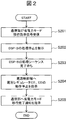
- FIG. 2 is a flowchart for explaining a processing flow when a digital signal processing unit DSP-A shown in FIG. 1 shifts to a power saving mode.
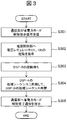
- FIG. 2 is a flowchart for explaining a processing flow when a power saving mode is canceled by the digital signal processor DSP-A shown in FIG. 1.
- the system block diagram which shows the internal structure of 2nd Embodiment of the physical quantity detection apparatus which concerns on this invention.
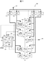
- FIG. 1 shows an internal configuration of a first embodiment of an angular velocity sensor as a physical quantity detection device according to the present invention.
- the illustrated angular velocity sensor 100 mainly includes an angular velocity sensor element (sensor element) 101, a capacitance detection unit (vibration direction displacement detection unit) 110, a drive signal generation unit (drive unit) 111, and a capacitance detection unit (Coriolis force displacement).
- (Quantity detection unit) 112 digital signal processing unit DSP-A (drive control value calculation unit) 122, digital signal processing unit DSP-B (physical quantity calculation unit) 123, communication unit 125, and power supply control unit 141 And a block (circuit unit).
- the angular velocity sensor element 101 includes a vibrator 102, fixed electrodes 108 and 109, electrodes 104 and 105, and fixed electrodes 106 and 107.
- the vibrator 102 of the angular velocity sensor element 101 has a predetermined mass and vibrates in a predetermined vibration axis direction at a predetermined vibration frequency.
- the fixed electrodes 108 and 109 apply an electrostatic force to adjust the vibration amplitude and vibration frequency in the vibration direction of the vibrator 102.
- the electrodes 104 and 105 detect the vibration amplitude and vibration frequency of the vibrator 102 by a change in capacitance.
- the fixed electrodes 106 and 107 detect a displacement generated in the vibrator 102 in a direction perpendicular to the vibration axis by a Coriolis force generated when an angular velocity is applied, based on a change in capacitance.
- the capacitance detection unit 110 detects the difference between the electrostatic capacitance between the angular velocity sensor element 101 and the fixed electrode 104 and the electrostatic capacitance between the angular velocity sensor element 101 and the fixed electrode 105, so that the vibration direction acting on the angular velocity sensor 101 is detected. , And the detection result is stored in a RAM (Read Only Memory) 121 via the bus line 120.
- RAM Read Only Memory
- the digital signal processing unit DSP-A 122 reads the displacement amount in the vibration direction of the vibrator 102 obtained by the capacitance detection unit 110 from the RAM 121, and the vibration in the driving direction of the vibrator 102 becomes the mechanical resonance vibration of the angular velocity sensor element 101.
- the frequency control value and the amplitude control value (drive control value) for the displacement amount are calculated so as to approach each other, and the calculation result is output to the drive signal generation unit 111 via the bus line 120.
- the drive signal generator 111 generates an AC drive signal that adjusts the frequency and amplitude according to the frequency control value and the amplitude control value output from the digital signal processor DSP-A 122, and the fixed electrode 108 based on the drive signal. And 109 are controlled to vibrate the angular velocity sensor element 101 at a predetermined frequency and amplitude.
- Such control by the capacitance detection unit 110, the digital signal processing unit DSP-A 122, and the drive signal generation unit 111 is feedback control, and the angular velocity sensor element 101 is made to reach and maintain its resonance vibration state.
- the capacitance detection unit 112 detects the difference between the capacitance between the vibrator 102 and the fixed electrode 106 and the capacitance between the vibrator 102 and the fixed electrode 107, so that the Coriolis force acting on the vibrator 102 is detected.
- the amount of displacement is detected, and the detection result is stored in the RAM 121 via the bus line 120.
- the digital signal processing unit DSP-B 123 reads the displacement amount of the vibrator 102 obtained by the capacitance detection unit 112 from the RAM 121, performs synchronous detection at the resonance frequency in the above-described resonance vibration state, and detects an amplitude value for the displacement amount.
- the detection result (amplitude value) is stored in the RAM 121.
- the digital signal processor DSP-B 123 performs a temperature correction operation on the amplitude value stored in the RAM 121 using a detection value by the temperature sensor 113 and a correction coefficient stored in advance in a ROM (Random Access Memory) 124.
- the offset depending on the temperature included in the detection result (amplitude value) is removed.
- the digital signal processing unit DSP-B 123 executes low-pass filter processing to remove high frequency noise components, and then stores the amplitude value in the RAM 121 as an angular velocity detection value.
- the communication unit 125 establishes data communication between the angular velocity sensor 100 and an external device.
- the angular velocity detection value obtained by the digital signal processing unit DSP-B 123 is read from the RAM 121 and is transmitted via the communication terminal 126 to a predetermined value.
- the communication unit 125 receives a power saving (low power consumption) mode switching signal (transition instruction signal or cancellation instruction signal) of the acceleration sensor 100 from the external device via the communication terminal 126.
- the communication unit 125 is a digital communication interface, for example, and may be a serial communication bus such as a 3-wire SPI bus or a 2-wire I2C bus.
- the above-described RAM 121 is a random access memory having a plurality of storage areas configured by, for example, SRAM (Static Random Access ⁇ Memory), and is a digital signal processor DSP-A122 or digital signal processor DSP-B123.
- SRAM Static Random Access ⁇ Memory
- DSP-A122 or digital signal processor DSP-B123 The processed calculation result can be stored, or a value in the middle of the calculation can be temporarily stored.
- the power supply control unit 141 includes a plurality of circuits such as the above-described capacitance detection unit 110 that receive a voltage supplied from an external power supply (for example, a vehicle-mounted battery) (not shown) provided outside the angular velocity sensor 100 via the power supply input terminal 130. It controls the operating state of the voltage regulators 131, 132, 134 and 135 that convert to the operating voltage of the block.
- an external power supply for example, a vehicle-mounted battery
- the voltage regulator 131 converts the voltage supplied from the external power source into the operating voltage of the capacitance detection unit 112 and the temperature sensor 113, and supplies the converted voltage to the capacitance detection unit 112 and the like.
- the voltage regulator 132 converts the voltage supplied from the external power source into the operating voltage of the capacitance detection unit 110 and the drive signal generation unit 111, and supplies the converted voltage to the capacitance detection unit 110 and the like.
- the voltage regulator 134 converts the voltage supplied from the external power source into the operating voltage of the RAM 121, the digital signal processing unit DSP-A 122, the communication unit 125, and the power source control unit 141, and supplies the converted voltage to the RAM 121 and the like. To do.
- the voltage regulator 135 converts the voltage supplied from the external power source into the operating voltage of the digital signal processing unit DSP-B123 and the ROM 124, and supplies the converted voltage to the digital signal processing unit DSP-B123.
- the power control unit 141 receives the voltage regulator 132.
- the voltage regulators 131 and 135 are in an operation stop state while the operation is in the operation state, and the voltage to the circuit blocks (capacitance detection unit 112, temperature sensor 113, digital signal processing unit DSP-B123, and ROM 124) connected to the voltage regulators 131 and 135 is stopped. Stop supplying.
- the communication unit 125 receives a power saving mode release instruction signal from an external device and accordingly receives an operation return (startup) instruction signal of each voltage regulator from the digital signal processing unit DSP-A 122. Then, the voltage regulators 131 and 135 are set in an operating state, and the voltage supply to the circuit blocks connected to them is resumed.
- FIGS. 2 and 3 specifically describe the processing flow when the digital signal processing unit DSP-A shown in FIG. 1 shifts to the power saving mode and cancels the power saving mode, respectively.
- the communication unit 125 when the communication unit 125 receives a transition instruction signal (switching signal) to the power saving mode from the external device during the transition to the power saving mode (S201), the digital signal processing unit DSP-A 122 Then, a processing stop instruction signal is output to the digital signal processor DSP-B123 (S202).
- the digital signal processing unit DSP-B123 receives the processing stop instruction signal from the digital signal processing unit DSP-A122, the digital signal processing unit DSP-B123 stops the operation after a series of processing sequences is completed (S203).
- the digital signal processor DSP-A 122 After confirming that the operation of the digital signal processor DSP-B 123 is stopped, the digital signal processor DSP-A 122 outputs an operation stop instruction signal for the voltage regulators 131 and 135 to the power supply controller 141 (S204). Further, the digital signal processing unit DSP-A 122 outputs a power saving mode transition completion notification instruction signal to the communication unit 125 (S205).
- the power supply control unit 141 receives the operation stop instruction signal of the voltage regulators 131 and 135 from the digital signal processing unit DSP-A 122, the power supply control unit 141 sets the voltage regulators 131 and 135 to the operation stop state.
- the communication unit 125 receives the power saving mode transition completion notification instruction signal from the digital signal processing unit DSP-A 122, the transition to the power saving mode of the angular velocity sensor 100 is completed for an external device (for example, a microcomputer) or the like. Notify you.
- an external device for example, a microcomputer
- the digital signal processing unit DSP-A122 when canceling the power saving mode, when the communication unit 125 receives a power saving mode canceling instruction signal (switching signal) from an external device (S301), the digital signal processing unit DSP-A122. Outputs an operation return (startup) instruction signal of the voltage regulators 131 and 135 to the power supply control unit 141 (S302). Thereafter, after the voltage supply to the digital signal processor DSP-B123 is resumed (S303), the digital signal processor DSP-A122 performs the processing sequence of the digital signal processor DSP-B123 at a timing synchronized with its own processing sequence. Is resumed (S304).
- the digital signal processing unit DSP-A 122 outputs a power saving mode release completion notification instruction signal to the communication unit 125 (S305).
- the communication unit 125 receives the power saving mode release completion notification instruction signal from the digital signal processing unit DSP-A 122, the communication unit 125 informs the external device (for example, a microcomputer) that the release of the power saving mode of the angular velocity sensor 100 has been completed. Notice.
- a plurality of voltage regulators particularly circuit blocks that need to maintain voltage supply during the power saving mode (circuit blocks necessary to maintain the resonance vibration of the angular velocity sensor element 101).
- the voltage regulator connected to the circuit block capable of stopping the voltage supply in the power saving mode, and the resonance of the angular velocity sensor element 101 of the angular velocity sensor 100 based on an external instruction signal for shifting to the power saving mode.
- the voltage regulator is selectively stopped so that the voltage is supplied only to the circuit block necessary for the processing for maintaining the vibration, and the voltage supply to the circuit block required for maintaining the resonance vibration of the angular velocity sensor element 101 is continued.
- the voltage supply to other circuit blocks is stopped.
- the voltage supply to each circuit block by the control of each voltage regulator is a circuit block (the angular velocity sensor element 101 of the angular velocity sensor element 101) that needs to maintain the voltage supply in the power saving mode.
- the digital signal processor DSP-A122 which is one of the circuit blocks required to maintain the resonance vibration, the voltage supply to each circuit block is reliably controlled in the power saving mode in which the power consumption is reduced. can do.
- FIG. 4 shows an internal configuration of a second embodiment of an angular velocity sensor as a physical quantity detection device according to the present invention.
- the second embodiment shown in FIG. 4 is different from the first embodiment shown in FIG. 1 in that two power inputs are provided, a voltage regulator is connected to one system, and a MOS switch is inserted to the other system.
- the other points are the same as in the first embodiment. Therefore, the same components as those in the first embodiment are denoted by the same reference numerals, and detailed description thereof is omitted.
- the angular velocity sensor 100A having such a configuration separates, for example, an analog circuit power source and a digital circuit power source, and independently supplies a voltage to each circuit. According to such a configuration, noise generated in the digital circuit can be prevented from leaking into the analog circuit through the power supply line. In addition, since the digital circuit is not easily affected by fluctuations in the power supply voltage, power can be directly supplied to the circuit block without using a voltage regulator.
- the MOS switch 302A is inserted in the power supply line connected to the digital signal processor DSP-B (physical quantity calculator) 123A and the ROM 124A that can stop the voltage supply in the power saving mode, By turning off the MOS switch 302A in the power saving mode, the same effects as those of the first embodiment can be realized.
- DSP-B digital signal processor
- the power control unit 141A, the RAM 121A, the digital signal processing unit DSP-A 122A, and the communication unit 125A, which are digital circuits, are connected to the external via the power input terminal 301A. Voltage is supplied directly from the power supply. Further, a MOS switch 302A is inserted into a power supply line connected to the digital signal processor DSP-B123A and the ROM 124A, and the digital signal processor DSP-B123A and the ROM 124A which are digital circuits are connected via a power input terminal 301A and the MOS switch 302A. A voltage is supplied from an external power source.
- a voltage is supplied from an external power source to the capacitance detection unit 112A and the temperature sensor 113A, which are analog circuits, via a power input terminal 130A and a voltage regulator 131A.
- a voltage is supplied from an external power source to the capacitance detection unit 110A and the drive signal generation unit 111A, which are analog circuits, via a power input terminal 130A and a voltage regulator 132A.
- the power supply control unit 141A controls the operating state of the voltage regulators 131A and 132A and the on / off of the MOS switch 302A, and the communication unit 125A receives a transition instruction signal from the external device to the power saving mode, and accordingly digital signal processing
- the voltage control unit 141A outputs the operation stop instruction signal to the voltage regulator 131A, and the voltage regulator 131A is turned on while the voltage regulator 132A is in the operation state.
- the operation is stopped, and voltage supply to the circuit blocks (capacitance detector 112A and temperature sensor 113A) connected to them is stopped.
- the power supply control unit 141A turns off the MOS switch 302A and stops the voltage supply to the circuit blocks (digital signal processing unit DSP-B 123A, ROM 124A) connected thereto.
- the communication unit 125A receives a power saving mode cancellation instruction signal from an external device, and the power supply control unit 141A receives an operation return (startup) instruction signal of each voltage regulator from the digital signal processing unit DSP-A 122A, the voltage The regulator 131A is set to the operating state, the MOS switch 302A is turned on, and the voltage supply to the circuit blocks connected thereto is resumed.
- the angular velocity sensor 100A of the second embodiment two power inputs are provided, a voltage regulator is provided only in one system, and a MOS switch is provided in the other system.
- the voltage regulator is selectively stopped so that the voltage is supplied only to the circuit block necessary for the process of maintaining the resonance vibration of the angular velocity sensor 100A based on the external instruction signal for transition to the power saving mode.
- the power switch mode is switched on and off, and the voltage supply to the circuit blocks required to maintain the resonance vibration of the angular velocity sensor element 101 is continued, and the voltage supply to the other circuit blocks is stopped, so that the power saving mode state is established.
- Reduced sensor function recovery time when canceling power saving mode while maintaining and reducing power consumption during power saving mode Rukoto can, can finely detect the desired angular velocity (physical quantity).
- the present invention is not limited to the first and second embodiments described above, and includes various modifications.
- the first and second embodiments described above have been described in detail for easy understanding of the present invention, and are not necessarily limited to those having all the configurations described.
- a part of the configuration of an embodiment can be replaced with the configuration of another embodiment, and the configuration of another embodiment can be added to the configuration of an embodiment.
- control lines and information lines indicate what is considered necessary for the explanation, and not all the control lines and information lines on the product are necessarily shown. Actually, it may be considered that almost all the components are connected to each other.
- angular velocity sensor 101 angular velocity sensor element (sensor element) 102 Vibrator 104, 105 Electrode 106, 107 Fixed electrode 108, 109 Fixed electrode 110 Capacitance detection unit (vibration direction displacement amount detection unit) 111 Drive signal generation unit (drive unit) 112 Capacity detector (Coriolis force displacement detector) 113 Temperature sensor 120 Bus line 121 RAM 122 Digital signal processor DSP-A (drive control value calculator) 123 Digital signal processor DSP-B (physical quantity calculator) 124 ROM 125 communication unit 126 communication terminal 130 power input terminals 131, 132, 134, 135 voltage regulator 141 power control unit 301A power input terminal 302A MOS switch
Landscapes
- Engineering & Computer Science (AREA)
- Physics & Mathematics (AREA)
- General Physics & Mathematics (AREA)
- Radar, Positioning & Navigation (AREA)
- Remote Sensing (AREA)
- Signal Processing (AREA)
- Gyroscopes (AREA)
- Pressure Sensors (AREA)
Abstract
消費電力を抑制した省電力モードで動作する角速度センサや加速度センサ等の物理量検出装置において、省電力モード時における消費電力を抑制しながら、当該物理量検出装置が正常に動作するまでの復帰時間を短縮して所望の物理量を精緻に検出することのできる物理量検出装置を提供する。 電源制御部141は、通信部125が省電力モードへの移行指示信号を受信した際に、駆動部111と振動方向変位量検出部110と駆動制御値算出部122と通信部125への電圧供給を継続すると共に、それ以外の回路部への電圧供給を停止する。
Description
本発明は、物理量検出装置に係り、例えば角速度や加速度等の物理量を検出する物理量検出装置に関する。
従来から、慣性センサの一種である角速度センサによって車体の回転角度をリアルタイムに検出し、車体の走行状態(例えば、横滑りや横転等)を制御する走行制御システムが知られている。また、慣性センサの一種である加速度センサによって携帯電話の傾斜を検知し、出力画面の方向を変化させるシステム等も知られている。このような慣性センサ、特にMEMS(Micro Electro Mechanical System)技術を用いて作成された慣性センサは、例えば固定電極と可動電極と慣性体(振動子)等から構成され、物理的な力によって慣性体が動作した量を固定電極と可動電極間の静電容量の変化から検出することで、慣性体に働いた物理量を算出する。
ところで、自動車等の車両の走行制御システムに搭載される電装機器は、駐停車の際のエンジン停止に起因するバッテリ電圧の低下、すなわち供給電圧の低下に対応する必要がある。そのため、例えば自動車分野においては、エンジンの運転状態を制御するエンジンコントロールユニット(ECU)により、エンジン停止時に前記電装機器を消費電力の少ない省電力モードに移行させる技術が採用されており、このような省電力モード時に慣性センサを振動させる技術が特許文献1に開示されている。
特許文献1に開示されている慣性センサ(角速度センサ)は、低消費エネルギーで大駆動振幅を得るために、常にセンサの固有振動数と一致した駆動信号を生成して当該角速度センサをその固有振動数で駆動させるものである。
ところで、例えば角速度センサ等の慣性センサは、該慣性センサに内蔵される振動子が所定の周波数と振幅で安定的に振動している状態で物理量(例えば角速度等)を検出する必要があるものの、その振動子は、一旦停止状態となると、その停止状態から安定的な振動状態に復帰するまでに所定の時間を要することが知れている。
上記した省電力モード時においては、消費電力をより一層抑制するために、電装機器に外部から供給される電圧(供給電圧)を一時的に所定値まで低下させたり、停止する(瞬断する)ことが考えられるものの、例えば角速度センサ等の慣性センサに対する電圧供給を停止すると、当該慣性センサが正常に動作するまでに時間を要し、所望の物理量を精緻に検出することが出来なくなるといった問題が生じ得る。
本発明は、前記課題に鑑みてなされたものであって、その目的とするところは、消費電力を抑制した省電力モードで動作する角速度センサや加速度センサ等の物理量検出装置において、省電力モード時における消費電力を抑制しながら、当該物理量検出装置が正常に動作するまでの復帰時間を短縮して所望の物理量を精緻に検出することのできる物理量検出装置を提供することにある。
上記する課題を解決するために、本発明に係る物理量検出装置は、振動子を有するセンサエレメントを用いて物理量を検出する物理量検出装置であって、該物理量検出装置は、省電力モードへの移行もしくは解除に関する切り替え信号を受信する通信部を含む複数の回路部と、該複数の回路部への電圧供給を制御する電源制御部と、を有し、前記電源制御部は、前記通信部が省電力モードへの移行指示信号を受信した際に、前記複数の回路部のうち前記センサエレメントの共振振動の維持に要する回路部への電圧供給を継続すると共に、それ以外の回路部への電圧供給を停止することを特徴とする。
本発明の物理量検出装置によれば、例えば消費電力を抑制した省電力モードにおいて外部電源からの電圧供給が一時的に低下した場合であっても、物理量検出装置を構成する複数の回路部のうちセンサエレメントの共振振動に関連する回路部への電圧供給のみを継続してセンサエレメントの動作を維持し、それ以外の回路部への電圧供給を停止することにより、省電力モード時における消費電力を抑制しながら、当該物理量検出装置が正常に動作するまでの復帰時間を短縮することができ、所望の物理量を精緻に検出することができる。
上記した以外の課題、構成及び効果は、以下の実施形態の説明により明らかにされる。
以下、本発明に係る物理量検出装置の実施形態を図面を参照して説明する。なお、以下では、主に物理量検出装置として角速度センサを採用した形態について説明するが、例えば加速度センサ等に適用し得ることは勿論である。
<第1実施形態>
図1は、本発明に係る物理量検出装置としての角速度センサの第1実施形態の内部構成を示したものである。
図1は、本発明に係る物理量検出装置としての角速度センサの第1実施形態の内部構成を示したものである。
図示する角速度センサ100は、主に、角速度センサエレメント(センサエレメント)101と、容量検出部(振動方向変位量検出部)110と駆動信号生成部(駆動部)111と容量検出部(コリオリ力変位量検出部)112とデジタル信号処理部DSP-A(駆動制御値算出部)122とデジタル信号処理部DSP-B(物理量算出部)123と通信部125と電源制御部141とを含む複数の回路ブロック(回路部)と、を備えている。
角速度センサエレメント101は、振動子102、固定電極108および109、電極104および105、固定電極106および107を備えている。
角速度センサエレメント101の振動子102は所定の質量を有し、所定の振動周波数で所定の振動軸方向に振動する。固定電極108および109は、振動子102の振動方向の振動振幅および振動周波数を調整するために静電気力を作用させる。電極104および105は、振動子102の振動振幅および振動周波数を静電容量の変化によって検出する。固定電極106および107は、角速度を印加すると生じるコリオリ力により前記振動軸と直交する方向に振動子102に生じる変位を静電容量の変化によって検出する。
容量検出部110は、角速度センサエレメント101と固定電極104の間の静電容量および角速度センサエレメント101と固定電極105の間の静電容量の差分を検出することにより、角速度センサ101に働く振動方向の変位量を検出し、その検出結果をバスライン120を介してRAM(Read Only Memory)121に格納する。
デジタル信号処理部DSP-A122は、RAM121から容量検出部110で得られた振動子102の振動方向の変位量を読み出し、振動子102の駆動方向の振動が角速度センサエレメント101の機械的共振振動に近づくようにその変位量に対する周波数制御値および振幅制御値(駆動制御値)を算出し、その算出結果をバスライン120を介して駆動信号生成部111へ出力する。
駆動信号生成部111は、デジタル信号処理部DSP-A122から出力された周波数制御値および振幅制御値に応じて周波数および振幅を調整する交流の駆動信号を生成し、その駆動信号に基づき固定電極108および109を制御して角速度センサエレメント101を所定の周波数および振幅で振動させる。
このような容量検出部110、デジタル信号処理部DSP-A122、および駆動信号生成部111による制御はフィードバック制御となっており、角速度センサエレメント101をその共振振動状態に到達させて維持する。
また、容量検出部112は、振動子102と固定電極106の間の静電容量および振動子102と固定電極107の間の静電容量の差分を検出することにより、振動子102に働くコリオリ力による変位量を検出し、その検出結果をバスライン120を介してRAM121に格納する。
デジタル信号処理部DSP-B123は、RAM121から容量検出部112で得られた振動子102の変位量を読み出し、上記の共振振動状態における共振周波数で同期検波を行い、その変位量に対する振幅値を検出し、その検出結果(振幅値)をRAM121に格納する。その後、デジタル信号処理部DSP-B123は、RAM121に格納した振幅値に対し、温度センサ113による検出値とROM(Random Access Memory)124に予め格納されている補正係数とを用いて温度補正演算を行い、検出結果(振幅値)に含まれる温度に依存したオフセットを除去する。また、デジタル信号処理部DSP-B123は、ローパスフィルタ処理を実行して高周波ノイズ成分を除去した後、その振幅値を角速度検出値としてRAM121へ格納する。
通信部125は、角速度センサ100と外部装置との間のデータ通信を成立させるもので、例えばデジタル信号処理部DSP-B123で得られた角速度検出値をRAM121から読み出し、通信端子126を介して所定の外部装置に送信する。また、通信部125は、通信端子126を介して外部装置から、加速度センサ100の省電力(低消費電力)モードの切り替え信号(移行指示信号又は解除指示信号)を受信する。ここで、通信部125は、例えばデジタル通信インタフェースであって、3線式のSPIバスや2線式のI2Cバス等のシリアル通信バスであってもよい。また、上記したRAM121は、例えばSRAM(Static Random Access Memory)で構成される複数の格納領域を有するランダム・アクセス・メモリであって、デジタル信号処理部DSP-A122やデジタル信号処理部DSP-B123で処理された演算結果を格納したり、演算途中の値を一時的に格納することができる。
電源制御部141は、電源入力端子130を介して角速度センサ100の外部に設けられた外部電源(例えば車載バッテリ)(不図示)から供給される電圧を上記した容量検出部110等の複数の回路ブロックの動作電圧へ変換する電圧レギュレータ131、132、134および135の動作状態を制御している。
ここで、電圧レギュレータ131は、外部電源から供給された電圧を容量検出部112および温度センサ113の動作電圧へ変換し、変換後の電圧を当該容量検出部112等へ供給する。また、電圧レギュレータ132は、外部電源から供給された電圧を容量検出部110および駆動信号生成部111の動作電圧へ変換し、変換後の電圧を当該容量検出部110等へ供給する。また、電圧レギュレータ134は、外部電源から供給された電圧をRAM121、デジタル信号処理部DSP-A122、通信部125、電源制御部141の動作電圧へ変換し、変換後の電圧を当該RAM121等へ供給する。また、電圧レギュレータ135は、外部電源から供給された電圧をデジタル信号処理部DSP-B123およびROM124の動作電圧へ変換し、変換後の電圧を当該デジタル信号処理部DSP-B123等へ供給する。
電源制御部141は、通信部125が外部装置から省電力モードへの移行指示信号を受信し、それに伴いデジタル信号処理部DSP-A122から各電圧レギュレータの動作停止指示信号を受けると、電圧レギュレータ132および134を動作状態としたままで、電圧レギュレータ131および135を動作停止状態とし、それらに繋がる回路ブロック(容量検出部112、温度センサ113、デジタル信号処理部DSP-B123、およびROM124)への電圧供給を停止する。
また、電源制御部141は、通信部125が外部装置から省電力モードの解除指示信号を受信し、それに伴いデジタル信号処理部DSP-A122から各電圧レギュレータの動作復帰(起動)指示信号を受けると、電圧レギュレータ131および135を動作状態とし、それらに繋がる回路ブロックへの電圧供給を再開する。
このような各電圧レギュレータの制御による各回路ブロックへの電圧供給は、主にデジタル信号処理部DSP-A122により制御されている。図2および図3はそれぞれ、図1に示すデジタル信号処理部DSP-Aによる省電力モード移行時および省電力モード解除時における処理フローを具体的に説明したものである。
図2に示すように、省電力モードへの移行時には、通信部125が外部装置から省電力モードへの移行指示信号(切り替え信号)を受信する(S201)と、デジタル信号処理部DSP-A122は、デジタル信号処理部DSP-B123へ処理停止指示信号を出力する(S202)。デジタル信号処理部DSP-B123は、デジタル信号処理部DSP-A122から処理停止指示信号を受信すると、一連の処理シーケンスが完了した後に動作を停止する(S203)。デジタル信号処理部DSP-A122は、デジタル信号処理部DSP-B123の動作停止を確認した後、電源制御部141に対し、電圧レギュレータ131および135の動作停止指示信号を出力する(S204)。また、デジタル信号処理部DSP-A122は、通信部125に対し、省電力モード移行完了通知指示信号を出力する(S205)。電源制御部141は、デジタル信号処理部DSP-A122から電圧レギュレータ131および135の動作停止指示信号を受けると、電圧レギュレータ131および135を動作停止状態とする。また、通信部125は、デジタル信号処理部DSP-A122から省電力モード移行完了通知指示信号を受信すると、外部装置(例えばマイコン)等に対して、角速度センサ100の省電力モードへの移行が完了したことを通知する。
一方で、図3に示すように、省電力モードの解除時には、通信部125が外部装置から省電力モードの解除指示信号(切り替え信号)を受信する(S301)と、デジタル信号処理部DSP-A122は、電源制御部141に対し、電圧レギュレータ131および135の動作復帰(起動)指示信号を出力する(S302)。その後、デジタル信号処理部DSP-B123への電圧供給が再開されてから(S303)、デジタル信号処理部DSP-A122は、自らの処理シーケンスに同期するタイミングでデジタル信号処理部DSP-B123の処理シーケンスを再開させる(S304)。また、デジタル信号処理部DSP-A122は、通信部125に対し、省電力モード解除完了通知指示信号を出力する(S305)。通信部125は、デジタル信号処理部DSP-A122から省電力モード解除完了通知指示信号を受信すると、外部装置(例えばマイコン)等に対して、角速度センサ100の省電力モードの解除が完了したことを通知する。
このように、本第1実施形態の角速度センサ100では、複数の電圧レギュレータ、特に省電力モード時に電圧供給を維持する必要のある回路ブロック(角速度センサエレメント101の共振振動の維持に要する回路ブロック)に繋がる電圧レギュレータと省電力モード時に電圧供給を停止し得る回路ブロックに繋がる電圧レギュレータを有し、外部からの省電力モードへの移行指示信号に基づいて、角速度センサ100の角速度センサエレメント101の共振振動を維持する処理に必要な回路ブロックのみに電圧が供給されるように選択的に電圧レギュレータを停止し、角速度センサエレメント101の共振振動の維持に要する回路ブロックへの電圧供給を継続すると共に、それ以外の回路ブロックへの電圧供給を停止する。これにより、省電力モード状態を維持して省電力モード時における消費電力を抑制しながら、省電力モード解除時のセンサ機能の復帰時間を短縮することができ、所望の角速度(物理量)を精緻に検出することができる。
また、各電圧レギュレータの制御による各回路ブロックへの電圧供給が、角速度センサ100を構成する複数の回路ブロックのうち、省電力モード時に電圧供給を維持する必要のある回路ブロック(角速度センサエレメント101の共振振動の維持に要する回路ブロック)の一つであるデジタル信号処理部DSP-A122によって制御されることにより、消費電力が低下した省電力モード時において、各回路ブロックへの電圧供給を確実に制御することができる。
<第2実施形態>
図4は、本発明に係る物理量検出装置としての角速度センサの第2実施形態の内部構成を示したものである。図4に示す第2実施形態は、図1に示す第1実施形態に対して、電源入力が二系統設けられ、一方の系統に電圧レギュレータが接続され、他方の系統にMOSスイッチが挿入されている点が相違しており、その他の構成は第1実施形態と同様である。したがって、第1実施形態と同様の構成には同様の符号を付してその詳細な説明は省略する。
図4は、本発明に係る物理量検出装置としての角速度センサの第2実施形態の内部構成を示したものである。図4に示す第2実施形態は、図1に示す第1実施形態に対して、電源入力が二系統設けられ、一方の系統に電圧レギュレータが接続され、他方の系統にMOSスイッチが挿入されている点が相違しており、その他の構成は第1実施形態と同様である。したがって、第1実施形態と同様の構成には同様の符号を付してその詳細な説明は省略する。
図4に示す第2実施形態の角速度センサ100Aは、二つの電源入力端子130A、301Aが設けられ、一方の電源入力端子130Aのみに電圧レギュレータ131A、132Aが接続されている。このような構成の角速度センサ100Aは、例えば、アナログ回路用電源とデジタル回路用電源を分離し、それぞれの回路に独立に電圧を供給するものである。このような構成によれば、デジタル回路で発生したノイズが、電源ラインを通してアナログ回路へ漏れ込むことを回避し得る。また、デジタル回路は電源電圧の変動の影響を受け難いことから、電圧レギュレータを介さずに直接的にその回路ブロックへ電源を供給することができる。また、このような構成の角速度センサ100Aでは、省電力モード時に電圧供給を停止させ得るデジタル信号処理部DSP-B(物理量算出部)123AやROM124Aに繋がる電源ラインにMOSスイッチ302Aを挿入し、前記省電力モード時に、このMOSスイッチ302AをOFF(オフ)することにより、上記した第1実施形態と同様の作用効果を実現し得る。
具体的には、本第2実施形態の角速度センサ100Aでは、デジタル回路である電源制御部141A、RAM121A、デジタル信号処理部DSP-A122A、および通信部125Aに、電源入力端子301Aを介して、外部電源から直接的に電圧が供給される。また、デジタル信号処理部DSP-B123AやROM124Aに繋がる電源ラインにMOSスイッチ302Aが挿入され、デジタル回路であるデジタル信号処理部DSP-B123AおよびROM124Aには、電源入力端子301AおよびMOSスイッチ302Aを介して、外部電源から電圧が供給される。
また、上記した第1実施形態の角速度センサ100と同様、アナログ回路である容量検出部112Aおよび温度センサ113Aには、電源入力端子130Aおよび電圧レギュレータ131Aを介して、外部電源から電圧が供給される。また、アナログ回路である容量検出部110Aおよび駆動信号生成部111Aには、電源入力端子130Aおよび電圧レギュレータ132Aを介して、外部電源から電圧が供給される。
電源制御部141Aは、電圧レギュレータ131Aおよび132Aの動作状態とMOSスイッチ302Aのオンオフを制御しており、通信部125Aが外部装置から省電力モードへの移行指示信号を受信し、それに伴いデジタル信号処理部DSP-A122Aから各電圧レギュレータの動作停止指示信号等を受けると、電圧制御部141Aは電圧レギュレータ131Aへ動作停止指示信号を出力し、電圧レギュレータ132Aを動作状態としたままで、電圧レギュレータ131Aを動作停止状態とし、それらに繋がる回路ブロック(容量検出部112A、温度センサ113A)への電圧供給を停止する。また、電源制御部141Aは、MOSスイッチ302Aをオフ状態とし、それらに繋がる回路ブロック(デジタル信号処理部DSP-B123A、ROM124A)への電圧供給を停止する。
なお、通信部125Aが外部装置から省電力モードの解除指示信号を受信し、電源制御部141Aがデジタル信号処理部DSP-A122Aから各電圧レギュレータの動作復帰(起動)指示信号等を受けると、電圧レギュレータ131Aを動作状態とし、MOSスイッチ302Aをオン状態とし、それらに繋がる回路ブロックへの電圧供給を再開する。
このように、本第2実施形態の角速度センサ100Aでは、電源入力が二系統設けられ、一方の系統のみに電圧レギュレータが配設され、他方の系統にMOSスイッチが配設されている場合であっても、外部からの省電力モードへの移行指示信号に基づいて、角速度センサ100Aの共振振動を維持する処理に必要な回路ブロックのみに電圧が供給されるように選択的に電圧レギュレータを停止したりMOSスイッチのオンオフを切り替え、角速度センサエレメント101の共振振動の維持に要する回路ブロックへの電圧供給を継続すると共に、それ以外の回路ブロックへの電圧供給を停止することにより、省電力モード状態を維持して省電力モード時における消費電力を抑制しながら、省電力モード解除時のセンサ機能の復帰時間を短縮することができ、所望の角速度(物理量)を精緻に検出することができる。
なお、本発明は上記した第1及び第2実施形態に限定されるものではなく、様々な変形形態が含まれる。例えば、上記した第1及び第2実施形態は本発明を分かりやすく説明するために詳細に説明したものであり、必ずしも説明した全ての構成を備えるものに限定されるものではない。また、ある実施形態の構成の一部を他の実施形態の構成に置き換えることが可能であり、また、ある実施形態の構成に他の実施形態の構成を加えることも可能である。また、実施形態の構成の一部について、他の構成の追加・削除・置換をすることが可能である。
また、制御線や情報線は説明上必要と考えられるものを示しており、製品上必ずしも全ての制御線や情報線を示しているとは限らない。実際には殆ど全ての構成が相互に接続されていると考えてもよい。
100 角速度センサ
101 角速度センサエレメント(センサエレメント)
102 振動子
104、105 電極
106、107 固定電極
108、109 固定電極
110 容量検出部(振動方向変位量検出部)
111 駆動信号生成部(駆動部)
112 容量検出部(コリオリ力変位量検出部)
113 温度センサ
120 バスライン
121 RAM
122 デジタル信号処理部DSP-A(駆動制御値算出部)
123 デジタル信号処理部DSP-B(物理量算出部)
124 ROM
125 通信部
126 通信端子
130 電源入力端子
131、132、134、135 電圧レギュレータ
141 電源制御部
301A 電源入力端子
302A MOSスイッチ
Claims (10)
- 振動子を有するセンサエレメントを用いて物理量を検出する物理量検出装置であって、
該物理量検出装置は、省電力モードへの移行もしくは解除に関する切り替え信号を受信する通信部を含む複数の回路部と、該複数の回路部への電圧供給を制御する電源制御部と、を有し、
前記電源制御部は、前記通信部が省電力モードへの移行指示信号を受信した際に、前記複数の回路部のうち前記センサエレメントの共振振動の維持に要する回路部への電圧供給を継続すると共に、それ以外の回路部への電圧供給を停止することを特徴とする物理量検出装置。 - 前記センサエレメントの共振振動の維持に要する回路部は、前記通信部と、前記センサエレメントを駆動させて振動させる駆動部と、前記センサエレメントの振動方向の変位量を検出する振動方向変位量検出部と、前記振動方向変位量検出部により検出された変位量に対する前記センサエレメントの駆動制御値を算出する駆動制御値算出部と、からなることを特徴とする、請求項1に記載の物理量検出装置。
- 前記電源制御部は、前記通信部が省電力モードへの移行指示信号を受信した際に、前記駆動制御値算出部から動作停止指示信号を受信して、前記それ以外の回路部への電圧供給を停止することを特徴とする、請求項2に記載の物理量検出装置。
- 前記それ以外の回路部は、前記センサエレメントの前記振動子のコリオリ力による変位量を検出するコリオリ力変位量検出部と、前記コリオリ力変位量検出部により検出された変位量から前記物理量を算出する物理量算出部と、を含むことを特徴とする、請求項2に記載の物理量検出装置。
- 前記通信部が省電力モードへの移行指示信号を受信した際に、前記駆動制御値算出部が前記コリオリ力変位量検出部へ処理停止指示信号を送信し、前記コリオリ力変位量検出部は、前記駆動制御値算出部から前記処理停止指示信号を受信した際に一連の処理シーケンスが完了した後に動作を停止し、前記駆動制御値算出部は、前記コリオリ力変位量検出部の動作の停止を確認した後に前記電源制御部へ動作停止指示信号を送信し、前記電源制御部は、前記駆動制御値算出部から前記動作停止指示信号を受信して前記コリオリ力変位量検出部と前記物理量算出部への電圧供給を停止することを特徴とする、請求項4に記載の物理量検出装置。
- 前記電源制御部は、外部電源と前記それ以外の回路部との間に配設される電圧レギュレータの動作を停止することにより、前記それ以外の回路部への電圧供給を停止することを特徴とする、請求項1に記載の物理量検出装置。
- 前記電源制御部は、外部電源と前記それ以外の回路部との間に配設されるMOSスイッチをオフすることにより、前記それ以外の回路部への電圧供給を停止することを特徴とする、請求項1に記載の物理量検出装置。
- 前記通信部は、前記物理量検出装置の省電力モードへの移行もしくは解除が完了した際に、外部装置に対して移行完了通知もしくは解除完了通知を送信することを特徴とする、請求項1に記載の物理量検出装置。
- 前記物理量検出装置は、前記複数の回路部に電圧を供給するための複数の外部入力端子を備えていることを特徴とする、請求項1に記載の物理量検出装置。
- 前記複数の外部入力端子は、前記複数の回路部のうちデジタル回路に接続される外部入力端子とアナログ回路に接続される外部入力端子とを含むことを特徴とする、請求項9に記載の物理量検出装置。
Priority Applications (1)
| Application Number | Priority Date | Filing Date | Title |
|---|---|---|---|
| JP2015544910A JPWO2015064349A1 (ja) | 2013-10-29 | 2014-10-14 | 物理量検出装置 |
Applications Claiming Priority (2)
| Application Number | Priority Date | Filing Date | Title |
|---|---|---|---|
| JP2013224035 | 2013-10-29 | ||
| JP2013-224035 | 2013-10-29 |
Publications (1)
| Publication Number | Publication Date |
|---|---|
| WO2015064349A1 true WO2015064349A1 (ja) | 2015-05-07 |
Family
ID=53003959
Family Applications (1)
| Application Number | Title | Priority Date | Filing Date |
|---|---|---|---|
| PCT/JP2014/077281 Ceased WO2015064349A1 (ja) | 2013-10-29 | 2014-10-14 | 物理量検出装置 |
Country Status (2)
| Country | Link |
|---|---|
| JP (1) | JPWO2015064349A1 (ja) |
| WO (1) | WO2015064349A1 (ja) |
Citations (8)
| Publication number | Priority date | Publication date | Assignee | Title |
|---|---|---|---|---|
| JPH1023106A (ja) * | 1996-07-03 | 1998-01-23 | Yazaki Corp | 信号伝送装置、信号伝送システム及び信号伝送方法 |
| JP2004272742A (ja) * | 2003-03-11 | 2004-09-30 | Seiko Epson Corp | 制御装置およびこれに用いられるプログラム並びに制御方法 |
| JP2005304146A (ja) * | 2004-04-08 | 2005-10-27 | Nidec Shibaura Corp | モータの駆動装置 |
| JP2006209744A (ja) * | 2004-12-27 | 2006-08-10 | Toshiba Corp | カードおよびホスト機器 |
| WO2007043504A1 (ja) * | 2005-10-11 | 2007-04-19 | Matsushita Electric Industrial Co., Ltd. | 振動型慣性力検知センサおよびそれを用いた電子機器 |
| JP2008182626A (ja) * | 2007-01-26 | 2008-08-07 | Seiko Epson Corp | 電源ユニット、被制御装置、および、通信システム |
| JP2009264974A (ja) * | 2008-04-25 | 2009-11-12 | Panasonic Corp | 慣性力センサ装置およびその起動制御方法 |
| JP2012177614A (ja) * | 2011-02-25 | 2012-09-13 | Sinfonia Technology Co Ltd | 加速度検出装置 |
-
2014
- 2014-10-14 WO PCT/JP2014/077281 patent/WO2015064349A1/ja not_active Ceased
- 2014-10-14 JP JP2015544910A patent/JPWO2015064349A1/ja active Pending
Patent Citations (8)
| Publication number | Priority date | Publication date | Assignee | Title |
|---|---|---|---|---|
| JPH1023106A (ja) * | 1996-07-03 | 1998-01-23 | Yazaki Corp | 信号伝送装置、信号伝送システム及び信号伝送方法 |
| JP2004272742A (ja) * | 2003-03-11 | 2004-09-30 | Seiko Epson Corp | 制御装置およびこれに用いられるプログラム並びに制御方法 |
| JP2005304146A (ja) * | 2004-04-08 | 2005-10-27 | Nidec Shibaura Corp | モータの駆動装置 |
| JP2006209744A (ja) * | 2004-12-27 | 2006-08-10 | Toshiba Corp | カードおよびホスト機器 |
| WO2007043504A1 (ja) * | 2005-10-11 | 2007-04-19 | Matsushita Electric Industrial Co., Ltd. | 振動型慣性力検知センサおよびそれを用いた電子機器 |
| JP2008182626A (ja) * | 2007-01-26 | 2008-08-07 | Seiko Epson Corp | 電源ユニット、被制御装置、および、通信システム |
| JP2009264974A (ja) * | 2008-04-25 | 2009-11-12 | Panasonic Corp | 慣性力センサ装置およびその起動制御方法 |
| JP2012177614A (ja) * | 2011-02-25 | 2012-09-13 | Sinfonia Technology Co Ltd | 加速度検出装置 |
Also Published As
| Publication number | Publication date |
|---|---|
| JPWO2015064349A1 (ja) | 2017-03-09 |
Similar Documents
| Publication | Publication Date | Title |
|---|---|---|
| US7849744B2 (en) | Driving device, physical quantity measurement device, and electronic instrument | |
| JP6307840B2 (ja) | 検出装置、センサー、電子機器及び移動体 | |
| CN104061923B (zh) | 检测装置、传感器、电子设备以及移动体 | |
| US7812681B2 (en) | Driver device, physical quantity measuring device, and electronic instrument | |
| US20080190198A1 (en) | Microelectromechanical gyroscope with suppression of capacitive coupling spurious signals and control method | |
| US10302431B2 (en) | Physical quantity detection circuit, electronic device, and moving object | |
| JP5136016B2 (ja) | 駆動装置、物理量測定装置及び電子機器 | |
| US20100206074A1 (en) | Oscillation drive device, physical quantity measurement device and electronic apparatus | |
| US20170276694A1 (en) | Circuit device, physical quantity detection device, electronic apparatus, and vehicle | |
| JP2019060794A (ja) | 物理量測定装置、電子機器及び移動体 | |
| JP2019082442A (ja) | 物理量測定装置、電子機器及び移動体 | |
| CN101990626A (zh) | 惯性力传感器 | |
| JP2014010149A (ja) | 慣性センサの自動利得制御装置および方法 | |
| KR20140086541A (ko) | 자이로센서의 구동 장치 | |
| JPWO2015064349A1 (ja) | 物理量検出装置 | |
| US7692506B2 (en) | Oscillation driver device, physical quantity measuring device, and electronic instrument | |
| JP5906397B2 (ja) | 慣性力センサ | |
| JP2012206687A (ja) | 信号処理回路、振動検出回路及び電子装置 | |
| JP6561702B2 (ja) | 物理量検出システム、電子機器及び移動体 | |
| JP2011002295A (ja) | 角速度検出装置 | |
| JP2012175766A (ja) | 走行体の振動発電駆動方法及び振動発電駆動装置 | |
| JP6465294B2 (ja) | 駆動回路、振動デバイス、電子機器及び移動体 | |
| JP2017040566A (ja) | 振動型ジャイロセンサ、電子機器及び移動体 | |
| US12338121B2 (en) | Electromechanical system and method for operating an electromechanical system | |
| JP5533525B2 (ja) | 角速度検出装置及び電子機器 |
Legal Events
| Date | Code | Title | Description |
|---|---|---|---|
| 121 | Ep: the epo has been informed by wipo that ep was designated in this application |
Ref document number: 14856833 Country of ref document: EP Kind code of ref document: A1 |
|
| ENP | Entry into the national phase |
Ref document number: 2015544910 Country of ref document: JP Kind code of ref document: A |
|
| NENP | Non-entry into the national phase |
Ref country code: DE |
|
| 122 | Ep: pct application non-entry in european phase |
Ref document number: 14856833 Country of ref document: EP Kind code of ref document: A1 |