WO2015060072A1 - 照明用モジュール、無線通信用モジュール、照明装置、および、照明制御システム - Google Patents
照明用モジュール、無線通信用モジュール、照明装置、および、照明制御システム Download PDFInfo
- Publication number
- WO2015060072A1 WO2015060072A1 PCT/JP2014/075938 JP2014075938W WO2015060072A1 WO 2015060072 A1 WO2015060072 A1 WO 2015060072A1 JP 2014075938 W JP2014075938 W JP 2014075938W WO 2015060072 A1 WO2015060072 A1 WO 2015060072A1
- Authority
- WO
- WIPO (PCT)
- Prior art keywords
- circuit
- coil
- capacitor
- wireless communication
- antenna
- Prior art date
- Legal status (The legal status is an assumption and is not a legal conclusion. Google has not performed a legal analysis and makes no representation as to the accuracy of the status listed.)
- Ceased
Links
Images

Classifications
-
- H—ELECTRICITY
- H01—ELECTRIC ELEMENTS
- H01Q—ANTENNAS, i.e. RADIO AERIALS
- H01Q9/00—Electrically-short antennas having dimensions not more than twice the operating wavelength and consisting of conductive active radiating elements
- H01Q9/04—Resonant antennas
- H01Q9/16—Resonant antennas with feed intermediate between the extremities of the antenna, e.g. centre-fed dipole
-
- H—ELECTRICITY
- H01—ELECTRIC ELEMENTS
- H01Q—ANTENNAS, i.e. RADIO AERIALS
- H01Q1/00—Details of, or arrangements associated with, antennas
- H01Q1/12—Supports; Mounting means
- H01Q1/22—Supports; Mounting means by structural association with other equipment or articles
-
- H—ELECTRICITY
- H05—ELECTRIC TECHNIQUES NOT OTHERWISE PROVIDED FOR
- H05B—ELECTRIC HEATING; ELECTRIC LIGHT SOURCES NOT OTHERWISE PROVIDED FOR; CIRCUIT ARRANGEMENTS FOR ELECTRIC LIGHT SOURCES, IN GENERAL
- H05B47/00—Circuit arrangements for operating light sources in general, i.e. where the type of light source is not relevant
- H05B47/10—Controlling the light source
- H05B47/175—Controlling the light source by remote control
- H05B47/19—Controlling the light source by remote control via wireless transmission
-
- H—ELECTRICITY
- H05—ELECTRIC TECHNIQUES NOT OTHERWISE PROVIDED FOR
- H05B—ELECTRIC HEATING; ELECTRIC LIGHT SOURCES NOT OTHERWISE PROVIDED FOR; CIRCUIT ARRANGEMENTS FOR ELECTRIC LIGHT SOURCES, IN GENERAL
- H05B45/00—Circuit arrangements for operating light-emitting diodes [LED]
Definitions
- the present invention relates to a lighting module, a wireless communication module, a lighting device, and a lighting control system.
- EMS Electronic Management System
- EMS can reduce power consumption and realize an energy-saving environment. Therefore, in recent years, EMS is often introduced into various buildings such as buildings, commercial facilities, and houses. Yes.
- EMS since it is necessary to control a device to be managed, it is indispensable to acquire information on the device to be managed and notify the device to be managed. Therefore, in EMS, it is necessary to mount a communication function on a device to be managed.
- Patent Document 1 Japanese Patent Laid-Open No. 2008-153831
- a wireless communication module and a wireless communication antenna that do not require wiring work are mounted on a lighting device. Then, it is conceivable to adopt a system in which control information and the like are transmitted to the lighting device by wireless communication.
- the installation space of lighting equipment is often limited, so that reliable lighting communication is realized in the lighting equipment while ensuring the lighting performance of the lighting equipment and without impairing the appearance of the lighting equipment. It is difficult to attach a wireless communication module or a wireless communication antenna.
- the present invention provides an illumination module, a wireless communication module, and an illumination module that perform reliable wireless communication while ensuring the illumination performance of the illumination device without impairing the appearance of the illumination device.
- An object is to realize an apparatus and a lighting control system.
- a first invention is an illumination module connectable to a wireless communication module, wherein the first circuit unit, the first capacitor, the second capacitor, and the second circuit unit are provided. , A module for lighting.
- the first circuit unit includes a light emitting element.
- the second circuit unit is connected to the first circuit and the wireless communication module, and includes a first capacitor, a second capacitor, and a first coil.
- the first end of the first capacitor is connected to the first connection terminal of the wireless communication module.
- the first end of the second capacitor is connected to the second connection terminal of the wireless communication module.
- the first coil has a first end connected to the second end of the first capacitor, and a second end connected to the second end of the second capacitor.
- the first circuit and the second circuit When a DC power source is connected to the first circuit unit and an AC signal having a first frequency is input between the first connection terminal and the second connection terminal of the wireless communication module, the first circuit and the second circuit
- the formed circuit functions as an antenna circuit with respect to an alternating current signal of the first frequency, and also functions as a circuit for lighting the light emitting element with respect to the direct current signal supplied from the direct current power source to the first circuit.
- the circuit formed by the first circuit and the second circuit functions as (1) a circuit for lighting a light emitting element with respect to a direct current component signal, and (2) a high frequency component signal (for example, , The first frequency AC signal) functions as a circuit constituting an antenna. That is, in this illumination module, it is possible to realize both an illumination circuit and an antenna circuit for wireless communication with a single circuit.
- this illumination module since it is not necessary to install a large antenna outside the illumination device as in the prior art in order to realize the wireless communication function, in the illumination device realized using this illumination module, , Without damaging its appearance.
- the lighting performance of the lighting device can be ensured without damaging the appearance of the lighting device, and highly reliable wireless communication can be executed.
- the lighting module according to the first aspect of the present invention may be configured such that a DC power source is connected to the first circuit unit, and an AC having a first frequency is connected between the first connection terminal and the second connection terminal of the wireless communication module.
- the circuit formed by the first circuit and the second circuit is: While functioning as an antenna circuit for the AC signal of the first frequency, “It functions as a circuit for lighting the light emitting element in response to a DC signal supplied from the DC power source to the first circuit”.
- the illumination module of the first invention is (1) By connecting a DC power source to the first circuit unit and inputting an AC signal (for example, a carrier wave signal for antenna transmission) between the first connection terminal and the second connection terminal of the wireless communication module, Functions as a transmitting antenna circuit and a light emitting element lighting circuit, (2) A DC power source is connected to the first circuit unit, and, for example, an antenna reception circuit is connected between the first connection terminal and the second connection terminal of the wireless communication module. It functions as a light emitting element lighting circuit.
- an AC signal for example, a carrier wave signal for antenna transmission
- the illumination module of the first invention can function as a transmitting antenna and a receiving antenna while functioning as a light emitting element lighting circuit.
- 2nd invention is 1st invention, Comprising: When making the circuit formed by a 1st circuit and a 2nd circuit function as an antenna circuit, let the carrier frequency of the radio signal to transmit / receive be fc, and in carrier frequency fc
- the inductive reactance of the first coil is XL (L1)
- the capacitive reactance of the first capacitor at the carrier frequency fc is Xc (C1)
- the capacitive reactance of the second capacitor is Xc (C2)
- XL (L1) 500 [ ⁇ ] Xc (C1) ⁇ 10 [ ⁇ ] Xc (C2) ⁇ 10 [ ⁇ ]
- the inductance value of the first coil, the capacitance value of the first capacitor, and the capacitance value of the second capacitor are set so as to satisfy the above.
- the impedance between the first end and the second end of the first coil is sufficiently high, and the first end and the second end of the first coil It can be approximated to a state in which the gap is electrically disconnected. Further, since the first capacitor and the second capacitor have sufficiently low impedance with respect to the signal having the carrier frequency fc, it can be approximated to a state in which the first capacitor and the second capacitor are directly connected.
- the impedance (inductive reactance) of the first coil is 0 ⁇
- the impedance (capacitive reactance) of the first capacitor and the second capacitor is infinite. Therefore, both ends of the first coil L1 are equivalent to being directly connected to a DC component signal, and both ends of the first capacitor and the second capacitor are equivalent to being electrically disconnected. It is.
- the circuit formed by the first circuit and the second circuit is ( 1) Functions as a circuit for lighting a light emitting element with respect to a DC component signal, and (2) Functions as a circuit constituting an antenna with respect to a high frequency component signal (for example, an AC signal of a first frequency). be able to.
- 3rd invention is 1st or 2nd invention, Comprising: A 1st circuit part is a several light emitting element, a 2nd coil, a 3rd coil, a 1st conductor pattern part, and a 2nd conductor pattern. A section.
- the plurality of light emitting elements of the first circuit portion, the second coil, the first conductor pattern portion, the first coil of the second circuit portion, the second conductor pattern of the first circuit portion, and the third coil are: Connected in series.
- the first conductor pattern portion is disposed between the second coil and the first coil.
- the second conductor pattern portion is disposed between the first coil and the third coil.
- the plurality of light emitting elements are connected in series so as to emit light when a direct current of a predetermined amount or more flows when a direct current power source is connected to the first circuit unit.
- the circuit formed by the first circuit and the second circuit is made to function as (1) a circuit for lighting the light emitting element with respect to the DC component signal, and (2) the high frequency component
- the first conductor pattern and the second conductor pattern can function as a circuit constituting the dipole antenna.
- 4th invention is 3rd invention, Comprising: When making the circuit formed by a 1st circuit and a 2nd circuit function as an antenna circuit, let the carrier frequency of the radio signal to transmit / receive be fc, and in carrier frequency fc When the inductive reactance of the second coil is XL (L2) and the inductive reactance of the third coil is XL (L3), XL (L2) ⁇ 500 [ ⁇ ] XL (L3) ⁇ 500 [ ⁇ ] The inductance value of the second coil and the inductance value of the third coil are set so as to satisfy the above.
- the second coil and the third coil have an impedance corresponding to the signal of the carrier frequency fc. It can be considered that the part is in an approximate state of being electrically disconnected. Therefore, in this illumination module, the first conductor pattern installed between the first coil and the second coil functions as one antenna element part of the dipole antenna with respect to the high-frequency signal of the carrier frequency fc, The 2nd conductor pattern installed between 1 coil and the 3rd coil functions as the other antenna element part of a dipole antenna.
- the circuit formed by the first circuit and the second circuit (1) functions as a circuit for lighting the light emitting element with respect to the DC component signal, and (2) the high frequency component
- the first conductor pattern and the second conductor pattern can function as a circuit constituting the dipole antenna.
- 5th invention is 3rd or 4th invention, Comprising:
- the carrier wave frequency of the radio signal to transmit / receive is set to fc, and a carrier wave
- the wavelength of the electromagnetic wave having the frequency fc is ⁇
- the relative permittivity of the material in the peripheral region where the first conductor pattern portion and the second conductor pattern portion are installed is ⁇ r
- the length of the first conductor pattern portion is d1.
- the wavelength shortening effect is an effect that, when a high-frequency signal (high-frequency electromagnetic wave) passes through a dielectric, the wavelength of the high-frequency signal that passes through the conductor portion is shortened due to the influence of the relative permittivity of the passing substance. . This phenomenon is also true when a high frequency signal passes through a conductor in a situation where a dielectric is disposed around the conductor.
- a material in the peripheral region where the first conductor pattern portion and the second conductor pattern portion are installed means, for example, when the first conductor pattern portion and the second conductor pattern portion are formed on the printed circuit board.
- 6th invention is 3rd or 4th invention, Comprising:
- the carrier wave frequency of the radio signal to transmit / receive is set to fc
- the wavelength of the electromagnetic wave having the frequency fc is ⁇
- the relative permittivity of the material in the peripheral region where the first conductor pattern portion and the second conductor pattern portion are installed is ⁇ r
- the length of the first conductor pattern portion is d1.
- the first conductor pattern portion and the second conductor pattern portion are formed so as to satisfy the function for obtaining the square root of x.
- this illumination module it is possible to realize a more accurate full-wavelength dipole antenna circuit in consideration of the wavelength shortening effect.
- the seventh invention is the first or second invention, wherein the first circuit section includes a plurality of light emitting elements, a third capacitor, a fourth coil, and a fifth coil.
- the fourth coil of the first circuit portion, the plurality of light emitting elements, the first coil of the second circuit portion, and the fifth coil of the first circuit portion are connected in series.
- the fourth coil of the first circuit unit has one end connected to a terminal set to the first potential when a DC power supply is connected to the first circuit unit, and the other end connected to one of the plurality of light emitting elements.
- the light emitting element is connected to the first end of the third capacitor.
- the fifth coil of the first circuit unit has one end connected to a terminal set to the second potential when a DC power source is connected to the first circuit unit, and the other end connected to the second end of the third capacitor. It is connected to the.
- the circuit formed by the first circuit and the second circuit (1) functions as a circuit for lighting the light emitting element with respect to the DC component signal, and (2) the high frequency component
- the first conductor pattern and the second conductor pattern can function as a circuit constituting a loop antenna.
- the “first potential” is, for example, a positive potential
- the “second potential” is, for example, a GND potential.
- the “first potential” and the “second potential” may be a combination of potentials such that when a plurality of light emitting elements are connected as described above, a forward bias is applied to the plurality of light emitting elements.
- the eighth invention is the seventh invention, wherein when the circuit formed by the first circuit and the second circuit functions as an antenna circuit, the carrier frequency of the radio signal to be transmitted and received is fc, and the carrier frequency at the carrier frequency fc If the inductive reactance of the fourth coil is XL (L4), the inductive reactance of the fifth coil is XL (L5), and the capacitive reactance of the third capacitor at the carrier frequency fc is Xc (C3), XL (L4) ⁇ 500 [ ⁇ ] XL (L5) ⁇ 500 [ ⁇ ] Xc (C3) ⁇ 10 [ ⁇ ] The inductance value of the fourth coil, the inductance value of the fifth coil, and the capacitance value of the third capacitor are set so as to satisfy the above.
- the fourth coil and the fifth coil have an impedance corresponding to the signal of the carrier frequency fc. It can be considered that the part is in an approximate state of being electrically disconnected.
- the impedance (capacitive reactance) of the third capacitor is sufficiently low at the carrier frequency fc, the third capacitor is electrically connected to the signal of the carrier frequency fc. It can be regarded as being in an approximate state of being directly connected.
- the first circuit and the first circuit are formed by a loop formed by the second coil, the third coil, the plurality of light emitting elements, and the first coil with respect to the high-frequency signal having the carrier frequency fc.
- Two circuits can function as a loop antenna.
- the circuit formed by the first circuit and the second circuit (1) functions as a circuit for lighting the light emitting element with respect to the DC component signal, and (2) the signal of the high frequency component
- the first conductor pattern and the second conductor pattern can function as a circuit constituting the loop antenna.
- a ninth invention is the seventh or eighth invention, wherein when the circuit formed by the first circuit and the second circuit functions as an antenna circuit, the carrier frequency of a radio signal to be transmitted and received is fc, The wavelength of the electromagnetic wave having the frequency fc is ⁇ , and is formed by the second end of the second capacitor, the second end of the third capacitor, the first end of the third capacitor, the plurality of light emitting elements, and the second end of the first capacitor.
- the first circuit and the second circuit are configured so as to form a loop that satisfies a function for obtaining the square root of x.
- the “relative permittivity of the material in the peripheral area where the loop is installed” is, for example, the relative permittivity of the material constituting the printed circuit board when the loop is formed on the printed circuit board. is there.
- the tenth invention is any one of the seventh to ninth inventions, wherein a capacitor is connected in parallel with at least one light emitting element of the plurality of light emitting elements of the first circuit portion.
- An eleventh aspect of the invention is any one of the first to tenth aspects of the invention, which is a wireless communication module that can be attached to and detached from the lighting module, and is connected to the second circuit portion of the lighting module so as to illuminate A wireless communication unit that performs wireless communication is provided via an antenna circuit formed by the first circuit and the second circuit of the module for use.
- the circuit formed by the first circuit and the second circuit of the illumination module can be changed to (1) a light emitting element for a DC component signal.
- a high frequency component signal for example, an AC signal having a first frequency
- the twelfth invention is formed by the first circuit and the second circuit of the illumination module by connecting to the illumination module according to any one of the first to tenth inventions and the second circuit portion of the illumination module. And a wireless communication module that performs wireless communication via an antenna circuit.
- an illuminating device including the illumination module and the wireless communication module can be realized.
- a thirteenth aspect of the invention is an illuminating device comprising the lighting module according to any one of the first to tenth aspects of the invention and the wireless communication module according to the eleventh aspect of the invention.
- an illuminating device including the illumination module and the wireless communication module can be realized.
- the fourteenth invention communicates with the master device, the lighting device according to the twelfth or thirteenth invention, the wireless communication module of the lighting device via the wireless communication network, and the master device via the wired network. And a slave device for communication.
- an illumination control system using the illumination device according to the twelfth or thirteenth invention can be realized.
- a lighting module a wireless communication module, a lighting device, and a lighting control that perform reliable wireless communication while ensuring the lighting performance of the lighting device without impairing the appearance of the lighting device.
- a system can be realized.
- the schematic block diagram of the illuminating device 100 which concerns on 1st Embodiment. Physical configurations of the first antenna unit A11, the second antenna unit A12, the coil L2, the coil L3, the first coil L1, the first capacitor C1, and the second capacitor C2 in the first circuit unit 11 and the second circuit unit 12. Showing an example (schematic configuration example).
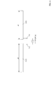
- FIG. 4 is a diagram showing an approximate circuit for a high-frequency signal in the circuit of FIG. 3.
- FIG. 9 is a diagram showing an approximate circuit for a high-frequency signal in the circuit of FIG. 8.
- the schematic block diagram of the illumination control system 3000 which concerns on 3rd Embodiment.
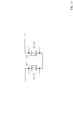
- the schematic block diagram which changed the connection pattern between light emitting elements in the illuminating device 200 of 2nd Embodiment.
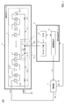
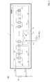
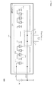
- FIG. 1 is a schematic configuration diagram of an illumination device 100 according to the first embodiment.
- the illumination device 100 includes an illumination module 1, a wireless communication module 2, and a power supply unit 3, as shown in FIG.
- the power supply unit 3 may be included in the illumination module 1.
- the illumination module 1 includes a first circuit unit 11 and a second circuit unit 12.
- the first circuit unit 11 includes n (n: natural number) light emitting elements (for example, light emitting diodes (LEDs)) LE1 to LEn, a coil L2, and a coil L3.
- n natural number
- light emitting elements for example, light emitting diodes (LEDs)
- LE1 to LEn a coil
- L2 coil
- L3 coil
- the light emitting element is described as a light emitting diode as an example.
- the n light emitting diodes LE1 to LEn are connected in series so that the anode is on the Vdc terminal side which is a DC power supply terminal.
- one end of the coil L2 is connected to the cathode of the light emitting diode LEn, and the other end of the coil L2 is connected to one end of the first coil L1 and one end of the first capacitor C1 of the second circuit unit 12. It is connected.
- one end of the coil L3 is connected to the end on the b point side of the first coil L1 of the second circuit portion 12 and the end on the b point side of the second capacitor C2.
- the other end of the coil L3 is connected to GND (GND terminal) as shown in FIG.
- the 2nd circuit part 12 is provided with the 1st coil L1, the 1st capacitor
- the end of the first coil L1 on the point a side is connected to one end of the coil L2 and the end of the first capacitor on the point a side.
- the end of the first coil L1 on the point b side is connected to one end of the coil L3 and the end of the second capacitor on the point b side.
- the first capacitor C1 has one end (end on the point a side) connected to the end on the point a side of the coil L1 and one end of the coil L2, and the other end is a module for wireless communication. 2 is connected to a connection terminal T11.
- the second capacitor C2 has one end (end on the b point side) connected to the end on the b point side of the coil L1 and one end of the coil L3, and the other end is a module for wireless communication. 2 is connected to a connection terminal T12.
- the portion (conductor pattern) indicated by A11 in FIG. 1 forms the first antenna portion A11, and the portion (conductor pattern) indicated by A12 in FIG. It is configured to form the second antenna part A12.
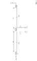
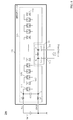
- FIG. 2 shows the first antenna unit A11, the second antenna unit A12, the coil L2, the coil L3, the first coil L1, the first capacitor C1, and the second capacitor in the first circuit unit 11 and the second circuit unit 12.
- An example (schematic configuration example) of the physical configuration of C2 is shown.
- the first antenna unit A11 is formed by forming an elongated rectangular conductor pattern (for example, a metal foil such as a copper foil) on a printed circuit board (not shown) for mounting electronic components. Configured.
- the first antenna portion A11 is formed as an elongated rectangular conductor pattern having a length d1 in the longitudinal direction.
- the second antenna unit A12 is formed by forming an elongated rectangular conductor pattern (for example, a metal foil such as a copper foil) on a printed board (not shown) for mounting electronic components. Configured.
- the second antenna portion A12 is formed as an elongated rectangular conductor pattern having a length d2 in the longitudinal direction.
- the length d1 of the conductor pattern of the first antenna part A11 in the longitudinal direction and the second antenna part A12 is preferably determined so as to satisfy the following relationship.
- the first antenna unit A11 and the second antenna unit A12 function as a half-wave dipole antenna
- a material around the conductor pattern of the first antenna unit A11 and the second antenna unit A12 Is the dielectric constant ⁇ r
- the conductor patterns of the first antenna part A11 and the second antenna part A12 are preferably formed so as to satisfy a function for obtaining the square root of x.
- the length d1 in the longitudinal direction of the conductor pattern of the first antenna unit A11 and the second antenna unit is preferably determined so as to satisfy the following relationship.
- the conductor patterns of the first antenna part A11 and the second antenna part A12 are preferably formed so as to satisfy a function for obtaining the square root of x.
- the first coil L1 and the first capacitor C1 connected to one end of the first antenna unit A11 are connected to one end of the first antenna unit A11 through a coated pattern or a conductive wire (wire) on the printed circuit board. It may be done.
- the coil L2 connected to the other end of the first antenna part A11 is connected to the other end of the first antenna part A11 via a coated pattern or a conductive wire (wire) on the printed circuit board. May be.
- first coil L1 and the second capacitor C2 connected to one end of the second antenna part A12 are connected to one end of the second antenna part A12 via a coated pattern or a conductive wire (wire) on the printed circuit board. It may be done.
- the coil L3 connected to the other end of the second antenna portion A12 is connected to the other end of the second antenna portion A12 via a coated pattern or a conductive wire (wire) on the printed circuit board. May be.
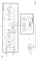
- the wireless communication module 2 includes a matching unit 21, an RF unit 22, and a communication control unit 23.
- the matching unit 21 includes a circuit (impedance adjustment circuit) that performs impedance adjustment.
- the impedance adjustment circuit of the matching unit 21 is connected to the second circuit unit 12 of the illumination module 1 via connection terminals T11 and T12 between the illumination module 1 and the wireless communication module 2, and performs impedance adjustment.
- the matching unit 21 may include a transmission impedance adjustment circuit and a reception impedance adjustment circuit.
- the matching unit 21 may include a circuit in which a transmission impedance adjustment circuit and a reception impedance adjustment circuit are shared.
- the matching unit 21 outputs the signal after impedance adjustment to the RF unit 22 when the illumination module 1 functions as a receiving antenna.
- the matching unit 21 inputs a signal from the RF unit 22, performs impedance adjustment on the input signal, and outputs the signal after impedance adjustment, It outputs to the 2nd circuit part 12 of the module 1 for illumination via connection terminal T11, T12.
- the RF unit 22 includes an antenna transmission processing unit (for example, an antenna transmission processing circuit) and an antenna reception processing unit (for example, an antenna reception processing circuit).
- the RF unit 22 inputs a command signal (control signal) from the communication control unit 23 and executes processing based on the command signal (control signal).
- the RF unit 22 When the illumination module 1 functions as a reception antenna, the RF unit 22 operates an antenna reception processing unit (for example, an antenna reception processing circuit) and performs an impedance adjustment signal output from the matching unit 21. Then, antenna reception processing (for example, processing including RF demodulation processing) is executed. Then, the RF unit 22 outputs a signal (information) acquired by antenna reception processing (for example, RF demodulation processing) to the communication control unit 23.
- antenna reception processing for example, processing including RF demodulation processing
- the RF unit 22 outputs a signal (information) acquired by antenna reception processing (for example, RF demodulation processing) to the communication control unit 23.
- the RF unit 22 operates an antenna transmission processing unit (for example, an antenna transmission processing circuit).
- the signal (information) output from the communication control unit 23 is RF-modulated, and the RF-modulated signal is output to the matching unit 21.
- the communication control unit 23 controls each functional unit of the wireless communication module 2.
- the communication control unit 23 is realized by, for example, a microprocessor.
- the communication control unit 23 is connected to the RF unit 22 and outputs a control signal to the RF unit 22 and information (signal) for performing RF modulation and antenna transmission.
- the communication control unit 23 detects that a radio wave is being transmitted from a lighting device other than its own device based on a signal from the RF unit 22, in order to prevent interference, collisions, etc.
- a control signal for stopping the RF modulation processing of the device itself may be output to the RF unit 22.
- the communication control unit 23 generates a power control signal Ctl based on a signal from the RF unit 22 and outputs the generated power control signal Ctl to the power supply unit 3.
- the wireless communication module 2 may be detachably connected to the illumination module 1 by a connector or the like.
- the wireless communication module 2 may be detachably connected to the power supply unit 3 by a connector or the like.
- the power supply unit 3 is connected to an AC power supply (not shown) and functions as a constant voltage source for the outside by converting AC current (or AC voltage) into DC current (or DC voltage).
- the power supply unit 3 is connected to the wireless communication module 2 and functions as a direct current power source that supplies a constant voltage DC_W to the wireless communication module 2.
- the power supply unit 3 is connected to the illumination module 1 via a Vdc terminal (and a GND terminal) that is a DC power supply terminal of the illumination module 1, and supplies a voltage DC_L to the illumination module 1. Functions as a DC power supply.
- the power supply unit 3 inputs a power supply control signal Ctl output from the communication control unit 23.
- the power supply unit 3 adjusts the value of the voltage DC_L supplied (output) to the illumination module 1 based on the power supply control signal Ctl.
- the power supply unit 3 may be detachably connected to the illumination module 1 by a connector or the like.
- the power supply unit 3 may be detachably connected to the wireless communication module 2 by a connector or the like.
- the lighting device 100 is functioned as an antenna for transmitting and receiving an electromagnetic wave having a carrier frequency f of 920 [MHz] will be described as an example.
- the inductance values and capacitance values (capacitance values) of the coils L2 and L3 of the first circuit unit 11, the first coil L1, the first capacitor C1, and the second capacitor C2 of the second circuit unit 12 are as follows: Set as follows.
- variables indicating the capacitance values of the first capacitor C1 and the second capacitor C2 are denoted as C1 and C2, respectively.
- the inductance value and the capacitance value are examples, and are not limited to the above values.
- the coils L2 and L3 of the first circuit unit 11, the first coil L1, the first capacitor C1, and the second capacitor C2 of the second circuit unit 12 are as follows.
- Xc (C1) Xc (C2) ⁇ 0.0173 [m ⁇ ]
- the inductive reactance XL of the first coil L1, the coil L2, and the coil L3 is expressed as XL (L1), XL (L2), and XL (L3), respectively.
- the capacitive reactances Xc of the first capacitor C1 and the second capacitor C2 are expressed as Xc (C1) and Xc (C2), respectively.
- the inductive reactance XL has a sufficiently high impedance
- the capacitive reactance Xc has a sufficiently low impedance
- the inductance value and the capacitance value (capacitance value) of the coils L2 and L3 of the first circuit unit 11, the first coil L1, the first capacitor C1, and the second capacitor C2 of the second circuit unit 12 are determined.
- the lighting apparatus 100 can realize both functions of the lighting control function and the antenna function.
- the figure shows a case where a direct current power source that supplies a voltage DC_L is connected to.
- the illumination module 1 of the illumination device 100 constitutes a circuit that realizes the illumination control function. That is, as shown in FIG. 4, the n light-emitting elements LE1 to LEn are forward-biased by the voltage DC_L applied between the Vdc terminal and the GND terminal, and the n light-emitting elements LE1 to LEn emit light. . Thereby, in the illuminating device 100, an illumination control function is realizable. Note that the amount of light emitted from the n light emitting elements LE1 to LEn can be adjusted by adjusting the voltage value of the voltage DC_L applied between the Vdc terminal and the GND terminal.
- the signal functions as a circuit that realizes an antenna function.
- the illuminating device 100 when all the n light emitting elements LE1 to LEn are turned off (initial state), (1) The illuminating device 100 receives a radio signal (electromagnetic wave) including information instructing to turn on the n light emitting elements LE1 to LEn of the illumination module 1 of the illuminating device 100 by wireless communication from the outside ( Antenna reception processing), (2) In accordance with the instruction information included in the received wireless signal, the illumination device 100 performs control to turn on the n light emitting elements LE1 to LEn of the illumination module 1 (illumination control processing), (3) Information indicating that the lighting device 100 is in a state where the n light emitting elements LE1 to LEn of the lighting module 1 are turned on and information indicating power consumption in the state are transmitted by radio signals (electromagnetic waves). , Transmitting from the lighting device 100 to the outside (antenna transmission processing), A specific operation of the lighting device 100 will be described below.
- the illuminating device 100 has a carrier frequency of 920 [MHz], and includes a radio signal including information instructing to turn on the n light emitting elements LE1 to LEn of the illumination module 1 of the illuminating device 100 (a signal indicating the information).
- a radio signal modulated using a carrier wave signal having a carrier frequency of 920 [MHz] is received by the first antenna unit A11 and the second antenna unit A12.
- the length d1 in the longitudinal direction of the conductor pattern of the first antenna unit A11 is set so that the antenna sensitivity with respect to a radio signal having a frequency of about 920 [MHz] is increased.
- the length d2 in the longitudinal direction of the conductor pattern of the second antenna part A12 is set.
- the first antenna unit A11 and the second antenna unit A12 function as a half-wave dipole antenna.
- the radio signals received by the first antenna unit A11 and the second antenna unit A12 are input to the matching unit 21 of the wireless communication module 2.
- the wireless signal input to the matching unit 21 is subjected to impedance adjustment processing in the matching unit 21, and the signal after impedance adjustment processing is output to the RF unit.
- RF signal processing for example, RF demodulation processing or the like
- information included in the wireless signal n pieces of the illumination module 1 of the lighting device 100.
- Information for instructing to light up the light emitting elements LE1 to LEn is acquired.
- the information acquired by the RF unit 22 is output to the communication control unit 23.
- the power supply unit 3 applies a DC voltage having a voltage value DC_L to the illumination module 1 based on the control signal Ctl output from the communication control unit 23 of the wireless communication module 2.
- a DC voltage having a voltage value DC_L is applied between the Vdc terminal, which is a DC power supply terminal of the illumination module 1, and the GND terminal. Since the first coil L1, the coil L2, and the coil L3 have an impedance (inductive reactance) with respect to a DC component of 0 ⁇ , a DC voltage having a voltage value DC_L is applied between the Vdc terminal and the GND terminal.
- a forward bias is applied to the light emitting elements LE1 to LEn, a direct current flows, and the n light emitting elements LE1 to LEn emit light. That is, the illumination device 100 lights up the n light emitting elements LE1 to LEn.
- the communication control unit 23 of the wireless communication module 2 performs the above-described illumination control process, and information indicating that the illumination device 100 is in a state where the n light emitting elements LE1 to LEn of the illumination module 1 are turned on. Then, information indicating the power consumption in the state is generated, and the generated information is output to the RF unit 22.
- the RF unit 22 generates a radio signal including the information output from the communication control unit 23 by performing RF modulation on the information output from the communication control unit 23 using a carrier wave signal having a carrier frequency of 920 [MHz]. . Then, the RF unit 22 outputs the generated radio signal to the matching unit 21.
- the matching unit 21 performs impedance adjustment processing on the radio signal output from the RF unit 22, and outputs the radio signal after impedance adjustment to the second circuit unit 12 of the illumination module 1.
- the circuit of the illumination module 1 functions as a dipole antenna for a high-frequency signal having a frequency of 920 [MHz]. Therefore, the wireless signal output from the wireless communication module 2 is radiated to the outside as an electromagnetic wave (wireless signal) by the first antenna unit A11 and the second antenna unit A12 of the illumination module 1.
- the circuit of the illumination module 1 functions as (1) a circuit for lighting the light emitting element with respect to the DC component signal, and (2) with respect to the high frequency component signal. Functions as a circuit constituting a dipole antenna. That is, in the lighting device 100, both a lighting circuit and an antenna circuit for wireless communication can be realized with one circuit.
- the illumination device 100 it is not necessary to install a large antenna outside the illumination device in order to realize the wireless communication function, so that the appearance of the illumination device is not impaired.
- the illumination module 1 when the illumination module 1 is installed in an elongated illumination tube having a hollow inside, the n light emitting elements are arranged in the longitudinal direction of the illumination tube, and the first antenna unit A11 and the second antenna unit are arranged. A region where the conductor pattern of A12 is formed can be easily secured, and further, the first antenna portion A11 and the second antenna portion are formed in a region where the antenna sensitivity is good (for example, a substantially central portion in the longitudinal direction of the illumination tube). It is also easy to form the conductor pattern of the antenna part A12.
- the lighting performance of the lighting device can be ensured and reliable wireless communication can be performed without deteriorating the appearance of the lighting device.
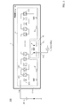
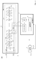
- FIG. 7 is a schematic configuration diagram of the illumination device 200 according to the second embodiment.
- the illumination device 200 of the second embodiment has a configuration in which the illumination module 1 is replaced with the illumination module 1A in the illumination device 100 of the first embodiment.
- the illumination module 1A has a configuration in which the first circuit unit 11 is replaced with the first circuit unit 11A in the illumination module 1 of the first embodiment.
- a coil L4 is installed between the Vdc terminal which is a DC power supply terminal and the point c in FIG. 7, and the points c and d in FIG. A capacitor C3 is installed between them.
- a coil L5 is installed between the point d in FIG. 7 and the GND terminal.
- the circuit of the illumination module 1A of the illumination device 200 configured as described above functions as a circuit for lighting the n light emitting elements LE1 to LEn for a direct current component signal, and for a high frequency component signal. Function as a circuit constituting a loop antenna.
- the coils L4 and L5 of the first circuit unit 11A, the first coil L1, the first capacitor C1, and the second capacitor C2 of the second circuit unit 12 are
- the inductive reactance XL of the first coil L1, the coil L4, and the coil L5 is expressed as XL (L1), XL (L4), and XL (L5), respectively.
- the capacitive reactances Xc of the first capacitor C1, the second capacitor C2, and the capacitor C3 are expressed as Xc (C1), Xc (C2), and Xc (C3), respectively.
- the inductive reactance XL has a sufficiently high impedance
- the capacitive reactance Xc has a sufficiently low impedance
- the inductance value and the capacitance value (capacitance value) of the coil L4, the coil L5, the capacitor C3 of the first circuit unit 11A, the first coil L1, the first capacitor C1, and the second capacitor C2 of the second circuit unit 12 are described.
- the lighting device 200 can realize both the illumination control function and the antenna function.
- the figure shows a case where a direct current power source that supplies a voltage DC_L is connected to.
- the illumination module 1A of the illumination device 200 constitutes a circuit that realizes the illumination control function. That is, as shown in FIG. 9, a voltage DC_L applied between the Vdc terminal and the GND terminal applies a forward bias to the n light emitting elements LE1 to LEn, and the n light emitting elements LE1 to LEn emit light. . Thereby, in the illuminating device 200, an illumination control function is realizable. Note that the amount of light emitted from the n light emitting elements LE1 to LEn can be adjusted by adjusting the voltage value of the voltage DC_L applied between the Vdc terminal and the GND terminal.
- the portion constituting the loop antenna for example, it is preferable to form a loop antenna by forming a conductor pattern (for example, a metal foil such as a copper foil) on the printed board of the illumination module 1A.
- the length of the path of the loop antenna formed by the points b, d, c, and a is d3
- the wavelength of the radio signal (electromagnetic wave) transmitted and received by the lighting device 200 is ⁇
- a function substantially similar to that of the loop antenna can be realized.
- the signal functions as a circuit that realizes an antenna function.
- the specific operation of the lighting device 200A is the same as that of the lighting device 100 of the first embodiment, and a detailed description thereof will be omitted.
- the circuit of the illumination module 1 functions as a circuit for lighting a light emitting element with respect to (1) a DC component signal, and (2) with respect to a high-frequency component signal. Functions as a circuit constituting a loop antenna. That is, in the lighting device 200, both a lighting circuit and an antenna circuit for wireless communication can be realized with one circuit.
- the appearance of the lighting device is not impaired.
- the n light emitting elements are arranged in the longitudinal direction of the illumination tube and a part of the conductor pattern of the loop antenna (part)
- the conductor pattern of the loop antenna can be formed in a region where the antenna sensitivity is good (for example, approximately the center in the longitudinal direction of the illumination tube). It is also easy to make it.
- the illumination performance of the lighting device can be ensured without damaging the appearance of the lighting device, and highly reliable wireless communication can be performed.
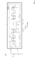
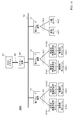
- FIG. 11 is a schematic configuration diagram of an illumination control system 3000 according to the third embodiment.
- the lighting control system 3000 includes a master device M1, a first slave device S1, a second slave device S2, and a third slave device S3 connected to a network N1 (wired network N1).
- the network N1 is, for example, a wired network using a dedicated line or a network (for example, a power line carrier communication network (PLC network)) that performs communication by modulating and superimposing a signal on a power line.
- PLC network power line carrier communication network
- the illumination control system 3000 is connected to a detachable wireless communication module WM11 and a detachable wireless communication module WM12 that are connected to the first slave device S1 by a wireless communication network W1. And an illumination module LM12.
- the illumination control system 3000 is connected to a detachable wireless communication module WM21 and a detachable wireless communication module WM22 that are connected to the second slave device S2 via a wireless communication network W2. And an illumination module LM22.
- the illumination control system 3000 includes an illuminance sensor SS31 connected to the third slave device S3 via a wireless communication network W3, and a human sensor SS32.
- the lighting control system 3000 includes one master device and three slave devices.
- the lighting control system 3000 is not limited to this configuration, and a plurality of master devices. And a plurality of slave devices.
- the removable wireless communication modules WM11, WM12, WM21, and WM22 are the same as the wireless communication module 2 described in the above embodiment, and can be attached to and detached from the illumination module by a connector or the like.
- the illumination modules LM11, LM12, LM21, and LM22 are the same as the illumination module 1 or 1A described in the above embodiment.
- illustration is abbreviate
- the illuminance detected by the illuminance sensor SS31 is in a low (dark) state
- the human sensor SS32 detects a person
- the plurality of light emitting elements of the illumination module LM11 are turned off.
- the control for turning on the light will be described below.
- the illuminance sensor SS31 transmits a signal including information indicating that the illuminance detected by the illuminance sensor SS31 is low (dark) to the third slave device S3 via the wireless communication network W3.
- the third slave device S3 transmits a signal including information acquired from the illuminance sensor SS31 via the wireless communication network W3 to the master device M1 via the wired network N1.
- the master device M1 acquires information about the illuminance detected by the illuminance sensor SS31 received via the wired network N1 from the third slave device S3, and holds the information.
- the human sensor SS32 when the human sensor SS32 detects a person, the human sensor SS32 transmits a signal including information indicating that the person has been detected to the third slave device S3 via the wireless communication network W3.
- the third slave device S3 transmits information received from the human sensor SS32 via the wireless communication network W3 (information indicating that a person has been detected) to the master device M1 via the wired network N1.
- the master device M1 acquires information indicating that a person has been detected by the human sensor SS32 based on a signal received from the third slave device S3 via the wired network N1. And the master apparatus M1 transmits the signal which instruct
- the first slave device S1 receives a signal transmitted from the master device M1 via the wired network N1, and transmits the received signal to the removable wireless communication module WM11 via the wireless communication network W1.
- the detachable wireless communication module WM11 receives a signal from the first slave device S1 via the wireless communication network W1. Specifically, the wireless signal from the first slave device S1 is received by operating the circuit of the illumination module LM11 as a reception antenna. Then, processing by the matching unit 21 (or 21A) and the RF unit 22 (or 22A) of the removable wireless communication module WM11 is performed on the received signal. Thereby, the communication control unit 23 (or 23A) of the removable wireless communication module WM11 acquires a signal instructing lighting of the plurality of light emitting elements of the illumination module LM11.
- the communication control unit 23 uses a predetermined voltage (predetermined adjustment) that allows the power supply unit 3 to turn on the light emitting elements LE1 to LEn of the illumination module 1 as the voltage supplied to the illumination module 1.
- a control signal Ctl for instructing to be a voltage for realizing the light rate is output to the power supply unit 3.
- the plurality of light emitting elements of the illumination module LM11 are turned on.
- the communication control unit 23 (or 23A) of the detachable wireless communication module WM11 outputs a signal including information on power consumed by lighting of the plurality of light emitting elements of the illumination module LM11 to the illumination module LM11. By operating the circuit as a transmission antenna, it may be controlled to be transmitted to the first slave device S1 via the wireless communication network W1.
- the first slave device S1 receives the signal transmitted from the removable wireless communication module WM11, and transmits the received signal to the master device M1 via the wired network N1.
- the master device M1 can grasp the amount of power consumed by the lighting module LM11 being lit from the signal received from the first slave device S1 via the wired network N1.
- the lighting control system 3000 by performing such processing, it is possible to grasp the power consumption acquired from each slave device and perform control such as turning off unnecessary lighting in order to realize energy saving.
- the master device M1 may be connected to the host system H1 via the network N2, and the information collected by the master device M1 may be transmitted to the host system H1.
- the host system H1 may instruct the master apparatus M1 to perform predetermined control based on the collected information.
- the detachable wireless communication module and the illumination module have been described for the case where the wireless communication is performed only with the slave device, but the present invention is not limited to this, and the detachable wireless communication module and the illumination module are not limited thereto. You may make it communicate by radio
- the illumination control system can be configured using the removable wireless communication module and the illumination module corresponding to the illumination devices 100 and 200 of the first and second embodiments. it can.
- the lighting control system 3000 only the slave device needs to have the communication functions of both the wired network and the wireless communication network, and the removable wireless communication module and the lighting module need only have the wireless communication function. . Thereby, in the lighting control system 3000, the total cost can be reduced when the system is constructed.
- the wireless communication module can be attached to and detached from the lighting module, the cost of the lighting module can be reduced. And since it is only necessary to load a detachable wireless communication module only to the illumination module to which a wireless communication function is to be added, it is possible to easily construct the illumination control system 3000 having flexibility and high expandability. Can do.
- the coil and the capacitor are described as one element.
- one coil may be realized by a plurality of coils connected in series or a plurality of coils connected in parallel.
- one capacitor may be realized by a plurality of capacitors connected in series or a plurality of capacitors connected in parallel.
- the coil inductance value, the capacitor capacitance value, the frequency of the radio signal, the wavelength, etc. are merely examples, and the values are set so as to include a predetermined allowable range and error range. You may make it set.
- the pattern for connecting the light emitting elements is not limited to the above embodiment, and the light emitting elements may be connected by other connection patterns.
- adjacent light emitting elements may be connected by a connection pattern as shown in FIG.
- a capacitor may be inserted in parallel to the light emitting element, and adjustment may be made so as to approach desired antenna characteristics.
- circuit may be realized in whole or in part by hardware, software, or a mixture of hardware and software.
Landscapes
- Engineering & Computer Science (AREA)
- Computer Networks & Wireless Communication (AREA)
- Circuit Arrangement For Electric Light Sources In General (AREA)
Applications Claiming Priority (2)
| Application Number | Priority Date | Filing Date | Title |
|---|---|---|---|
| JP2013222234A JP6271214B2 (ja) | 2013-10-25 | 2013-10-25 | 照明用モジュール、無線通信用モジュール、照明装置、および、照明制御システム |
| JP2013-222234 | 2013-10-25 |
Publications (1)
| Publication Number | Publication Date |
|---|---|
| WO2015060072A1 true WO2015060072A1 (ja) | 2015-04-30 |
Family
ID=52992675
Family Applications (1)
| Application Number | Title | Priority Date | Filing Date |
|---|---|---|---|
| PCT/JP2014/075938 Ceased WO2015060072A1 (ja) | 2013-10-25 | 2014-09-29 | 照明用モジュール、無線通信用モジュール、照明装置、および、照明制御システム |
Country Status (2)
| Country | Link |
|---|---|
| JP (1) | JP6271214B2 (enExample) |
| WO (1) | WO2015060072A1 (enExample) |
Cited By (4)
| Publication number | Priority date | Publication date | Assignee | Title |
|---|---|---|---|---|
| WO2018041923A1 (en) | 2016-09-05 | 2018-03-08 | Philips Lighting Holding B.V. | Led-filament and lighting device comprising the led-filament. |
| WO2021228589A1 (en) * | 2020-05-12 | 2021-11-18 | Signify Holding B.V. | System of lamps for a luminaire |
| CN114073168A (zh) * | 2019-07-04 | 2022-02-18 | 昕诺飞控股有限公司 | 基于发光二极管led的照明设备以及对应的led板和驱动器板 |
| CN116232361A (zh) * | 2021-12-06 | 2023-06-06 | 台湾禾邦电子有限公司 | 可携式电子装置及其具有发光功能的天线模块 |
Families Citing this family (3)
| Publication number | Priority date | Publication date | Assignee | Title |
|---|---|---|---|---|
| JP6692048B2 (ja) * | 2016-04-25 | 2020-05-13 | パナソニックIpマネジメント株式会社 | 照明器具及び照明システム |
| US20200037423A1 (en) * | 2016-09-27 | 2020-01-30 | Lucis Technologies (Shanghai) Co., Ltd. | Dimming control for lighting systems and methods thereof |
| KR102730027B1 (ko) | 2017-02-10 | 2024-11-14 | 삼성전자주식회사 | 조명 장치 및 조명 시스템 |
Citations (3)
| Publication number | Priority date | Publication date | Assignee | Title |
|---|---|---|---|---|
| JP2002289372A (ja) * | 2001-03-28 | 2002-10-04 | Hitachi Ltd | 無線アンテナ付き照明装置、照明システム及び照明器具と無線アンテナ部材 |
| JP2004303445A (ja) * | 2003-03-28 | 2004-10-28 | Ebara Densan Ltd | 電飾装置 |
| JP2012521706A (ja) * | 2009-03-24 | 2012-09-13 | コーニンクレッカ フィリップス エレクトロニクス エヌ ヴィ | 遠隔制御信号受信器を有する発光デバイスシステム、及びドライバ |
Family Cites Families (2)
| Publication number | Priority date | Publication date | Assignee | Title |
|---|---|---|---|---|
| AU2002334568A1 (en) * | 2002-09-05 | 2004-03-29 | Agency For Science, Technology And Research | A method and an apparatus for controlling the rate of a video sequence; a video encoding device |
| JP5147161B2 (ja) * | 2005-03-02 | 2013-02-20 | ソニーモバイルコミュニケーションズ株式会社 | 携帯無線端末およびアンテナモジュール |
-
2013
- 2013-10-25 JP JP2013222234A patent/JP6271214B2/ja not_active Expired - Fee Related
-
2014
- 2014-09-29 WO PCT/JP2014/075938 patent/WO2015060072A1/ja not_active Ceased
Patent Citations (3)
| Publication number | Priority date | Publication date | Assignee | Title |
|---|---|---|---|---|
| JP2002289372A (ja) * | 2001-03-28 | 2002-10-04 | Hitachi Ltd | 無線アンテナ付き照明装置、照明システム及び照明器具と無線アンテナ部材 |
| JP2004303445A (ja) * | 2003-03-28 | 2004-10-28 | Ebara Densan Ltd | 電飾装置 |
| JP2012521706A (ja) * | 2009-03-24 | 2012-09-13 | コーニンクレッカ フィリップス エレクトロニクス エヌ ヴィ | 遠隔制御信号受信器を有する発光デバイスシステム、及びドライバ |
Cited By (6)
| Publication number | Priority date | Publication date | Assignee | Title |
|---|---|---|---|---|
| WO2018041923A1 (en) | 2016-09-05 | 2018-03-08 | Philips Lighting Holding B.V. | Led-filament and lighting device comprising the led-filament. |
| CN114073168A (zh) * | 2019-07-04 | 2022-02-18 | 昕诺飞控股有限公司 | 基于发光二极管led的照明设备以及对应的led板和驱动器板 |
| WO2021228589A1 (en) * | 2020-05-12 | 2021-11-18 | Signify Holding B.V. | System of lamps for a luminaire |
| CN115606320A (zh) * | 2020-05-12 | 2023-01-13 | 昕诺飞控股有限公司(Nl) | 用于照明器的灯的系统 |
| US12200844B2 (en) | 2020-05-12 | 2025-01-14 | Signify Holding B.V. | Systems and methods for wireless intra-luminaire communication and control of separate lamps |
| CN116232361A (zh) * | 2021-12-06 | 2023-06-06 | 台湾禾邦电子有限公司 | 可携式电子装置及其具有发光功能的天线模块 |
Also Published As
| Publication number | Publication date |
|---|---|
| JP2015084295A (ja) | 2015-04-30 |
| JP6271214B2 (ja) | 2018-01-31 |
Similar Documents
| Publication | Publication Date | Title |
|---|---|---|
| JP6271214B2 (ja) | 照明用モジュール、無線通信用モジュール、照明装置、および、照明制御システム | |
| US10805999B2 (en) | Lighting connectivity module | |
| KR101700443B1 (ko) | 원격 제어 신호 수신기를 포함하는 발광 디바이스 시스템 및 드라이버 | |
| US8633646B2 (en) | Method and apparatus for radio-frequency controllable LED lamp fixture antenna | |
| JP2000504890A (ja) | 小型の無線周波送受信アンテナおよびこのアンテナを用いる制御デバイス | |
| WO2013077171A1 (ja) | 可視光通信用照明器具及び同器具を用いた可視光通信システム | |
| EP3622580B1 (en) | An antenna structure, for different range communication modes | |
| JP4824672B2 (ja) | 照明器具電極をアンテナとして使用する装置及び方法 | |
| JP2015115287A (ja) | 照明用モジュール、無線通信用モジュール、照明装置、および、照明制御システム | |
| JP6575228B2 (ja) | アンテナモジュール及び無線通信装置 | |
| CN216122448U (zh) | 信号可视化的无线信号屏蔽器 | |
| JP2024074309A (ja) | 照明装置および照明システム | |
| US9554427B2 (en) | Radio transmission between modules in a potential-separated LED converter | |
| JP6295074B2 (ja) | 無線通信装置、照明装置、照明用モジュール、無線通信用モジュール、および、照明制御システム | |
| JP7588608B2 (ja) | 発光ダイオード(led)ベースの照明デバイス、並びに対応するled基板及びドライバ基板 | |
| EP4460887A1 (en) | Transmitter device with visualization unit for wirelessly powering receiver devices | |
| JP2024090791A (ja) | 照明装置 | |
| JP2024086121A (ja) | 照明装置 | |
| JP2020057839A (ja) | 無線ユニットおよび照明器具 | |
| JP2013141141A (ja) | ワイヤレス通信システム | |
| CA3035483A1 (en) | Electronic converter |
Legal Events
| Date | Code | Title | Description |
|---|---|---|---|
| 121 | Ep: the epo has been informed by wipo that ep was designated in this application |
Ref document number: 14855013 Country of ref document: EP Kind code of ref document: A1 |
|
| NENP | Non-entry into the national phase |
Ref country code: DE |
|
| 122 | Ep: pct application non-entry in european phase |
Ref document number: 14855013 Country of ref document: EP Kind code of ref document: A1 |