WO2015046380A1 - 電子機器 - Google Patents
電子機器 Download PDFInfo
- Publication number
- WO2015046380A1 WO2015046380A1 PCT/JP2014/075524 JP2014075524W WO2015046380A1 WO 2015046380 A1 WO2015046380 A1 WO 2015046380A1 JP 2014075524 W JP2014075524 W JP 2014075524W WO 2015046380 A1 WO2015046380 A1 WO 2015046380A1
- Authority
- WO
- WIPO (PCT)
- Prior art keywords
- antenna
- band
- sub
- feeding point
- electronic device
- Prior art date
- Legal status (The legal status is an assumption and is not a legal conclusion. Google has not performed a legal analysis and makes no representation as to the accuracy of the status listed.)
- Ceased
Links
Images

Classifications
-
- G—PHYSICS
- G01—MEASURING; TESTING
- G01S—RADIO DIRECTION-FINDING; RADIO NAVIGATION; DETERMINING DISTANCE OR VELOCITY BY USE OF RADIO WAVES; LOCATING OR PRESENCE-DETECTING BY USE OF THE REFLECTION OR RERADIATION OF RADIO WAVES; ANALOGOUS ARRANGEMENTS USING OTHER WAVES
- G01S19/00—Satellite radio beacon positioning systems; Determining position, velocity or attitude using signals transmitted by such systems
- G01S19/01—Satellite radio beacon positioning systems transmitting time-stamped messages, e.g. GPS [Global Positioning System], GLONASS [Global Orbiting Navigation Satellite System] or GALILEO
- G01S19/13—Receivers
- G01S19/35—Constructional details or hardware or software details of the signal processing chain
- G01S19/36—Constructional details or hardware or software details of the signal processing chain relating to the receiver frond end
-
- H—ELECTRICITY
- H01—ELECTRIC ELEMENTS
- H01Q—ANTENNAS, i.e. RADIO AERIALS
- H01Q21/00—Antenna arrays or systems
- H01Q21/30—Combinations of separate antenna units operating in different wavebands and connected to a common feeder system
-
- H—ELECTRICITY
- H01—ELECTRIC ELEMENTS
- H01Q—ANTENNAS, i.e. RADIO AERIALS
- H01Q3/00—Arrangements for changing or varying the orientation or the shape of the directional pattern of the waves radiated from an antenna or antenna system
- H01Q3/26—Arrangements for changing or varying the orientation or the shape of the directional pattern of the waves radiated from an antenna or antenna system varying the relative phase or relative amplitude of energisation between two or more active radiating elements; varying the distribution of energy across a radiating aperture
- H01Q3/2605—Array of radiating elements provided with a feedback control over the element weights, e.g. adaptive arrays
Definitions
- the present invention relates to an electronic device.
- An electronic device such as a mobile phone may have a receiving antenna that receives a signal from an artificial satellite of a satellite positioning system such as GPS (Global Positioning System). It is desirable to improve the performance of such a receiving antenna.
- GPS Global Positioning System
- One aspect of the electronic apparatus includes a first receiving antenna that receives a signal from an artificial satellite of a satellite positioning system, a multi-antenna having a second receiving antenna, and a first feeding point that is common to the first and second receiving antennas.
- the first receiving antenna is disposed closer to the corner of the electronic device than the second receiving antenna.
- the performance of the receiving antenna that receives signals from satellites in the satellite positioning system can be improved.
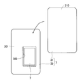
- FIG. 1 is a perspective view illustrating an appearance of an electronic device according to a first embodiment.
- FIG. 3 is a back view showing the appearance of the electronic apparatus according to the first embodiment.
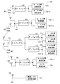
- 3 is a diagram illustrating a configuration of a wireless processing unit according to Embodiment 1.
- FIG. It is a figure which shows the structure of the various antennas which concern on Embodiment 1, and a battery side case main body.
- FIG. 3 is a back view showing the appearance of the electronic apparatus according to the first embodiment.
- 3 is a partial enlarged view of a battery-side case body according to Embodiment 1.
- FIG. 6 is a diagram illustrating a configuration of a wireless processing unit according to Embodiment 2.
- FIG. It is a figure which shows the structure of the various antennas which concern on Embodiment 2, and a battery side case main body. 6 is a partially enlarged view of a battery-side case body according to Embodiment 2.
- FIG. 1 is a perspective view illustrating an appearance of
- FIG. 1 is a perspective view illustrating an outline of an appearance of an electronic device 1 according to the first embodiment.
- Electronic device 1 according to the present embodiment is a mobile phone such as a smartphone, for example.
- the electronic device 1 includes a device case 4 including a display side case 2 and a battery side case 3.
- the electronic device 1 (device case 4) has a substantially rectangular plate shape in plan view.
- a transparent display region 21 is provided on the outer surface 20 of the display side case 2, that is, on the front surface of the device case 4.
- the user can visually recognize various information such as characters displayed on a display unit such as a liquid crystal display provided in the device case 4 through the display area 21.
- a receiver hole 5 is provided in the upper end 20 a of the outer surface 20 of the display side case 2.
- a receiver is provided in the device case 4, and the received sound output from the receiver is output to the outside of the electronic device 1 through the receiver hole 5. Further, the camera lens 6 provided in the device case 4 is visible from the upper end portion 20 a of the outer surface 20 of the display side case 2.
- the upper side and the lower side in the present embodiment are the upper side and the lower side when the user makes a call by placing the electronic device 1 held in his / her hand on the ear. It is. Normally, when the user makes a call, the electronic device 1 is held in the hand with the portion having the receiver hole 5 on the upper side, so that the receiver hole 5 in the electronic device 1 is on the upper side.
- the device case 4 In addition to the display unit, the receiver, and the camera lens 6, various parts are housed in the device case 4.
- the device case 4 for example, a printed board on which electronic components are mounted, a metal plate that reinforces the device case 4, a battery, and the like are stored.
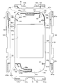
- FIG. 2 is a plan view showing an outline of the appearance of the electronic device 1 when the electronic device 1 is viewed from the back side.
- the battery side case 3 includes a battery side case body 30 and a cover member 31.
- the battery side case body 30 houses the battery 7 and is attached to the display side case 2.
- the cover member 31 is attached to the battery side case body 30 from the back side of the electronic device 1.
- FIG. 2 shows the battery side case 3 in a state where the cover member 31 is removed from the battery side case body 30.
- the cover member 31 is attached to the battery side case body 30 so as to cover the outer surface 301 of the battery side case body 30.
- the outer surface 310 of the cover member 31 is the back surface of the electronic device 1 (the back surface of the device case 4).
- An opening 300 is provided in the battery side case body 30.
- the battery 7 is housed in the battery-side case body 30 through the opening 300.
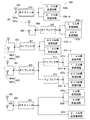
- the electronic device 1 is provided with a wireless processing unit 100 that performs wireless communication with other communication devices.
- FIG. 3 is a diagram illustrating a configuration of the wireless processing unit 100.
- the wireless processing unit 100 can wirelessly communicate with a base station using wireless signals of 2.5G band, 1.9G band, and 800M band.
- radio processing section 100 includes 2.5G band, 1.9G band, and 800M band radio signals in LTE (Long Term Evolution), and 1.9G band in CDMA (Code Division Multiple Access).
- 800M band wireless signals can be transmitted and received.
- the wireless processing unit 100 can receive a wireless signal from a satellite positioning system, for example, a GPS artificial satellite.
- the wireless processing unit 100 can wirelessly communicate with a communication device using a wireless LAN, for example, WiFi.
- a radio signal from a GPS artificial satellite is referred to as a “GPS signal”.
- the wireless processing unit 100 includes a first antenna group 101 that transmits and receives a 2.5 G band radio signal, a second antenna group 102 that transmits and receives a 1.9 G band radio signal, and an 800 M band. And a third antenna group 103 for transmitting and receiving the wireless signal.
- the first antenna group 101 can transmit and receive a 2.5 G-band radio signal called “B41” in LTE.
- the second antenna group 102 can transmit and receive a 1.9G band radio signal called "B25" in LTE and a 1.9G band radio signal called "BC1" in CDMA.
- the three antenna group 103 includes an 800M band radio signal called “B26” in LTE, an 800M band radio signal called “BC0” in CDMA, and an 800M band radio signal called “BC10” in CDMA. Can be transmitted and received.
- the wireless processing unit 100 also includes a GPS antenna 104 that receives GPS signals and a wireless LAN antenna 105 that transmits and receives wireless signals over a wireless LAN.
- the GPS signal is a 1.5 G band radio signal.
- a wireless signal transmitted / received by the wireless LAN antenna 105, in this example, a wireless signal using WiFi is a 2.4G band wireless signal.
- the 2.5G band first antenna group 101 includes a main antenna 101m that performs transmission and reception and a sub-antenna 101s that performs only reception.
- transmission is performed using only the main antenna 101m during transmission
- reception is performed using the main antenna 101m and the sub antenna 101s during reception. That is, the first antenna group 101 functions as a multi-antenna only during reception.
- the second antenna group 102 of the 1.9G band includes a main antenna 102m that performs transmission and reception, and a sub antenna 102s that performs only reception. Similar to the first antenna group 101, the second antenna group 102 transmits only by the main antenna 102m at the time of transmission, and receives by the main antenna 102m and the sub antenna 102s at the time of reception. That is, the second antenna group 102 functions as a multi-antenna only during reception.
- the third antenna group 103 in the 800M band includes a main antenna 103m that performs transmission and reception, and a sub antenna 103s that performs only reception. As with the first antenna group 101 and the second antenna group 102, the third antenna group 103 transmits only the main antenna 103m when transmitting, and receives the main antenna 103m and the sub antenna 103s when receiving. . That is, the third antenna group 103 functions as a multi-antenna only during reception.
- each of first antenna group 101, second antenna group 102, and third antenna group 103 receives a MIMO (Multiple (Input Multiple Output) signal from the base station at the time of reception. Used as an antenna.
- MIMO Multiple (Input Multiple Output) signal from the base station at the time of reception. Used as an antenna.
- At least one of the first antenna group 101, the second antenna group 102, and the third antenna group 103 may be used as a multi-antenna other than the multi-antenna for MIMO.
- at least one of the first antenna group 101, the second antenna group 102, and the third antenna group 103 may be used as a multi-antenna for an adaptive array that controls at least one of an antenna directivity beam and a null.
- at least one of the first antenna group 101, the second antenna group 102, and the third antenna group 103 may be used as a multi-antenna for diversity.
- the wireless processing unit 100 is provided with a 2.5G band transmission circuit 130s, a 1.9G band transmission circuit 131s, an 800M band transmission circuit 132s, and a wireless LAN transmission / reception circuit 134.
- the wireless processing unit 100 includes two 2.5G band receiving circuits 130r-m and 130r-s, two 1.9G band receiving circuits 131r-m and 131r-s, and two 800M band receiving circuits 132r-. m, 132r-s and a GPS receiving circuit 133r are provided.
- the wireless processing unit 100 is provided with an RF switch (high frequency switch) 110, two duplexers 111 and 112, and three diplexers 120 to 122.
- the RF switch 110 is connected to the feeding point 153 of the 2.5G band main antenna 101m
- the diplexer 120 is connected to the feeding point 150 of the 2.5G band sub-antenna 101s and the 1.9G band sub-antenna 102s.
- the diplexer 121 is connected to the feeding point 151 of the 1.9G band main antenna 102m and the 800M band main antenna 103m
- the diplexer 122 is connected to the 800M band sub antenna 103s and the feeding point 152 of the GPS antenna 104. ing.
- ⁇ About transmission processing> In each of the 2.5G band transmission circuit 130s, 1.9G band transmission circuit 131s, 800M band transmission circuit 132s, and wireless LAN transmission / reception circuit 134, a transmission signal generated by a control unit (not shown) that controls the wireless processing unit 100 is received. Entered.
- the 2.5G band transmission circuit 130s performs up-conversion processing and amplification processing on the input transmission signal to generate a 2.5G band transmission signal.
- the transmission signal generated by the 2.5G band transmission circuit 130s is input to the main antenna 101m through the RF switch 110. As a result, a 2.5G band radio signal is transmitted from the main antenna 101m.
- the 1.9G band transmission circuit 131s performs an up-conversion process and an amplification process on the input transmission signal to generate a 1.9G band transmission signal.
- the 1.9G band transmission signal is input to the main antenna 102m through the duplexer 111 and the diplexer 121. As a result, a 1.9G band radio signal is transmitted from the main antenna 102m.
- the 800G band transmission circuit 132s performs an up-conversion process and an amplification process on the input transmission signal to generate an 800M band transmission signal.
- the 800M band transmission signal is input to the main antenna 103m through the duplexer 112 and the diplexer 121. As a result, a radio signal in the 800M band is transmitted from the main antenna 103m.
- the wireless LAN transmission / reception circuit 134 performs up-conversion processing, amplification processing, and the like on the input transmission signal to generate a 2.4G band transmission signal.
- the 2.4G band transmission signal is input to the wireless LAN antenna 105.
- the wireless LAN antenna 105 transmits a wireless signal in the 2.4G band over WiFi.
- a reception signal received by the 2.5G band main antenna 101m is input to the 2.5G band reception circuit 130r-m through the RF switch 110.
- the 2.5G band reception circuit 130r-m performs amplification processing, down-conversion processing, and the like on the input reception signal, and outputs the processed reception signal to the control unit.
- the received signal received by the 2.5G band sub-antenna 101s is input to the 2.5G band receiving circuit 130r-s through the diplexer 120.
- the 2.5G band reception circuit 130r-s performs amplification processing, down-conversion processing, and the like on the input reception signal, and outputs the processed reception signal to the control unit.
- the control unit performs demodulation processing or the like on the received signals output from the 2.5G band receiving circuits 130r-m and 130r-s, and includes control data included in the 2.5G band radio signal transmitted from the base station. And user data and the like are reproduced.
- the reception signal received by the 1.9G band sub-antenna 102s is input to the 1.9G band reception circuit 131r-s through the diplexer 120.
- the 1.9G band reception circuit 131r-s performs amplification processing, down-conversion processing, and the like on the input reception signal, and outputs the processed reception signal to the control unit.
- a reception signal received by the 1.9G band main antenna 102m is input to the 1.9G band receiving circuit 131r-m through the diplexer 121 and the duplexer 111.
- the 1.9G band reception circuit 131r-m performs amplification processing, down-conversion processing, and the like on the input reception signal, and outputs the processed reception signal to the control unit.
- the control unit performs demodulation processing or the like on the reception signals output from the 1.9G band reception circuits 131r-m and 131r-s, and includes control data included in the 1.9G band radio signal transmitted by the base station. And user data and the like are reproduced.
- the reception signal received by the main antenna 103m in the 800M band is input to the 800M band receiving circuit 132r-m through the diplexer 121 and the duplexer 112.
- the 800M band reception circuit 132r-m performs amplification processing, down-conversion processing, and the like on the input reception signal, and outputs the processed reception signal to the control unit.
- a reception signal received by the 800M band sub-antenna 103s is input to the 800M band reception circuit 132r-s through the diplexer 122.
- the 800M band reception circuit 132r-s performs amplification processing, down-conversion processing, and the like on the input reception signal, and outputs the processed reception signal to the control unit.
- the control unit performs demodulation processing and the like on the reception signals output from the 800M band reception circuits 132r-m and 132r-s, and includes control data and user data included in the 800M band radio signal transmitted from the base station. Play.
- the reception signal received by the GPS antenna 104 is input to the GPS reception circuit 133r through the diplexer 122.
- the GPS reception circuit 133r performs amplification processing, down-conversion processing, and the like on the input reception signal and outputs the processed reception signal to the control unit.
- the control unit performs demodulation processing or the like on the received signal input from the GPS receiving circuit 133r, and reproduces control data, user data, and the like included in the received signal.
- the reception signal received by the wireless LAN antenna 105 is input to the wireless LAN transmission / reception circuit 134.
- the wireless LAN transmission / reception circuit 134 performs amplification processing, down-conversion processing, and the like on the input reception signal, and outputs the processed reception signal to the control unit.
- the control unit performs demodulation processing or the like on the reception signal input from the wireless LAN transmission / reception circuit 134, and reproduces control data, user data, and the like included in the reception signal.
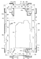
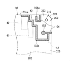
- FIG. 4 is a diagram showing the structure of various antennas provided in the wireless processing unit 100 and the structure of the battery-side case body 30.
- FIG. 4 is a front view of the battery-side case body 30.
- a top view, a bottom view, a left side view, and a right side view of the battery side case body 30 are shown on the upper side, the lower side, the left side, and the right side of FIG.
- the battery side case body 30 is shown as viewed from the side where the cover member 31 is attached.
- Various antennas such as the main antenna 101m provided in the wireless processing unit 100 are formed of, for example, a conductor pattern. Further, the feeding points 150 to 154 connected to the antenna are also formed by a conductor pattern, for example.
- the various antennas and feed points 150 to 154 are formed on the outer surface 301 of the battery-side case body 30 by, for example, printing a metal material mainly composed of silver. Each of the feeding points 150 to 154 has a round shape, for example.
- the battery side case body 30 has a substantially shallow box shape.
- An outer surface 301 of the substantially box-shaped battery-side case body 30 includes a substantially rectangular main surface 302 in plan view, an upper side surface 303 (referred to as “upper side surface 303”), and a lower side surface 304 (“lower side”).
- a side surface 305 (referred to as “left side 305”) and a right side surface 306 (referred to as “right side 306”).
- the main surface 302 is formed with the above-described opening 300 into which the battery 7 is inserted.
- four screw holes 310 are formed at four corners of the main surface 302, respectively.
- the left side and the right side of the battery side case body 30 in the present embodiment are the upper side of the battery side case body 30 (the electronic device 1 held by the user in the hand) as shown in the center of FIG. On the left side and the right side when the battery side case body 30 is viewed from the side where the cover member 31 is attached. is there.
- the boundary portion 323 between the main surface 302 and the upper surface 303 is not angular and is curved. That is, the main surface 302 is curved from the end portion on the upper surface 302 side to the end portion on the main surface 302 side in the upper surface 302.
- the boundary portion 324 between the main surface 302 and the lower surface 304 is not angular and is curved.
- a boundary portion 325 between the main surface 302 and the left side surface 305 is not angular and is curved.
- a boundary portion 324 between the main surface 302 and the lower surface 304 is not angular and is curved.
- the upper right corner 320, the upper left corner 321, the lower left corner 322, and the lower right corner 323 of the battery side case body 30 are not angular and are curved (rounded).
- the 800 M band sub antenna 103 s and the GPS antenna 104 which share the feeding point 152, are formed in the upper right corner portion 350 of the battery side case body 30.
- the sub antenna 103 s and the GPS antenna 104 are formed near the upper right corner 320 of the battery side case body 30.
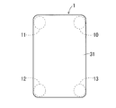
- the sub antenna 103s and the GPS antenna 104 are viewed from the cover member 31 side (back side) as shown in FIG. Is formed in the upper right corner portion 10 on the inner side of the electronic device 1.
- 5 also shows an upper left corner portion 11, a lower left corner portion 12, and a lower right corner portion 13 inside the electronic device 1 when the electronic device 1 is viewed from the cover member 31 side.
- the feeding point 152 is provided on the main surface 302 side of the upper right corner portion 350 of the battery side case body 30. In other words, the feeding point 152 is provided near the upper right corner of the main surface 302 of the battery-side case body 30.
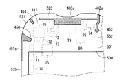
- FIG. 6 is an enlarged view showing the vicinity of the upper right corner portion 350 of the battery side case body 30.
- an earphone jack 40 housed in the device case 4 is located below the upper right corner portion 350 of the battery-side case body 30.
- Parts such as the vibrator 41, the side key 42, and the proximity sensor 43 are located. If parts exist under the sub antenna 103s and the GPS antenna 104, the performance of the sub antenna 103s and the GPS antenna 104 may deteriorate. Therefore, the sub antenna 103s and the GPS antenna 104 should not be positioned as much as possible on the parts. Placed in. Similarly, other antennas included in the wireless processing unit 100 are also arranged so as not to be positioned as much as possible on the components in the device case 4.
- the GPS antenna 104 extends from the feeding point 152 toward the right side 306 so as not to pass over the nearby side key 42, and the curved portion 306a (right side) of the right side 306 is formed. 306 extends to the flat portion 306b of the right side surface 306. In other words, the GPS antenna 104 extends from the feeding point 152 toward the right side 306, passes through the curved boundary portion 326 between the main surface 302 and the right side 306, and extends to the flat portion 306 b of the right side 306. Yes.
- the GPS antenna 104 extends from the flat portion 306 b on the right side surface 306 to the flat portion 303 b on the upper side surface 303 through the upper right corner 320 that is curved on the battery side case body 30.
- the GPS antenna 104 extends from the flat portion 303b of the upper side surface 303 to a curved boundary portion 323 between the upper side surface 303 and the main surface 302, and then ends by making a U-turn 180 degrees to the left. .
- the open end 104 a of the GPS antenna 104 is located outside the feeding point 152. Specifically, the open end 104 a of the GPS antenna 104 is located outside the feeding point 152 at the peripheral edge of the battery-side case body 30.
- the 800M band sub-antenna 103s temporarily extends slightly from the feeding point 152 toward the right side 306, and then extends 180 degrees U-turn downward toward the left side 305.
- the sub-antenna 103 s extending toward the left side surface 305 is bent 90 degrees toward the upper side surface 303 and extends toward the upper side surface 303 when slightly exceeding the feeding point 152.
- the sub-antenna 103 s directed toward the upper side 303 extends obliquely in a staircase shape while slightly moving toward the left side 305 so as to avoid the nearby vibrator 41, earphone jack 40 and proximity sensor 43.
- the open end 103sa of the sub antenna 103s is located outside the feeding point 152, like the open end 104a of the GPS antenna 104. Specifically, the open end 103sa of the sub-antenna 103s is located outside the feeding point 152 at the peripheral edge of the battery-side case body 30.
- the GPS antenna 104 is arranged on the upper right corner 320 side of the 800M band sub antenna 103s.
- the GPS antenna 104 is arranged on the corner side of the electronic device 1 relative to the 800M band sub-antenna 103s (when the electronic device 1 is viewed from the cover member 31 side, It is arranged on the upper right corner side of the device 1. Therefore, it is difficult for parts in the electronic device 1 to exist near the GPS antenna 104. Therefore, it can suppress that the performance of the GPS antenna 104 deteriorates under the influence of the components in the device case 4. That is, the performance of the GPS antenna 104 can be improved.
- control part in the electronic device 1 calculates
- the electronic device 1 when an emergency call is made from the electronic device 1 to the police or the like, the electronic device 1 notifies the police or the like of the position of the electronic device 1 in order for the police or the like to specify the position of the user. There is. At this time, if the position of the electronic device 1 notified to the police or the like is not correct, it becomes difficult for the police or the like to accurately specify the position of the user. In the present embodiment, since the performance of the GPS antenna 104 is improved, the accuracy of the position of the electronic device 1 required by the control unit can be improved. Therefore, the electronic device 1 can notify the police or the like of the correct position of the electronic device 1 when making an emergency call to the police or the like.
- the open end of the antenna such as the GPS antenna 104 is located on the inner side rather than the outer side of the battery side case body 30, a ground plane formed on a printed circuit board or the like in the device case 4 It becomes easy to combine. As a result, antenna performance may be degraded. In other words, when the open end of the antenna such as the GPS antenna 104 is located inside rather than outside in the electronic device 1, it becomes easy to couple with the ground plane in the electronic device 1, and the antenna performance. May deteriorate.
- the open end 104a of the GPS antenna 104 and the open end 103sa of the sub-antenna 103s are located outside the feed point 152, and in detail, power is fed at the periphery of the battery-side case body 30. Since it is located outside the point 152, it is difficult to couple with the ground plane in the device case 4. Therefore, the performance of the GPS antenna 104 and the sub antenna 103s is improved. Considering a state in which the battery side case body 30 is incorporated in the electronic device 1, it can be said that the open end 104 a of the GPS antenna 104 and the open end 103 sa of the sub antenna 103 s are located on the inner peripheral edge of the electronic device 1. .
- the GPS antenna 104 is arranged so that its open end 104 a is located outside the feeding point 152 without passing inside the feeding point 152. Therefore, the GPS antenna 104 can be disposed closer to the end (more toward the corner) in the electronic device 1. Therefore, the GPS antenna 104 is less affected by the components in the device case 4 and the performance is improved.
- the sub-antenna 103s extends from the feeding point 152 toward the right side 306, and then extends in the right side 306 toward the lower side 304 in one direction.
- the open end 103sa can be arranged outside the feeding point 152.
- the 800M band sub-antenna 103s is longer than the GPS antenna 104, when the sub-antenna 103s extends in one direction in the right side surface 306 toward the lower side surface 304, the open end 103sa of the sub antenna 103s becomes the right side surface. It may reach the center in the longitudinal direction at 306. Then, in a state where the electronic device 1 is held in the user's hand, the sub antenna 103s is easily covered with the user's hand. As a result, the performance of the sub antenna 103s may be degraded.
- the sub-antenna 103 s passes through the inside of the feeding point 152 at the end in the battery-side case body 30, and the open end 103 sa of the sub-antenna 103 s is located outside the feeding point 152.
- the open end 103sa can be disposed outside the long sub-antenna 103s without extending it in one direction. Therefore, the sub antenna 103s is not easily covered with the user's hand. As a result, the performance of the sub antenna 103s is improved.
- the 2.5 G band sub-antenna 101 s and the 1.9 G band sub antenna 102 s, which share the feeding point 150, are formed in the upper left corner portion 351 of the battery-side case body 30.
- the sub-antennas 101 s and 102 s have an upper left corner portion 11 inside the electronic device 1 when the electronic device 1 is viewed from the cover member 31 side. (See FIG. 5).
- the feeding point 150 is provided on the main surface 302 side of the upper left corner portion 351 of the battery side case body 30. In other words, the feeding point 150 is provided near the upper left corner of the main surface 302 of the battery side case body 30.
- the required performance of the 2.5G band sub-antenna 101s is higher than the required performance of the 1.9G band sub-antenna 102s.
- the signal loss allowed in the 2.5G band sub-antenna 101s is smaller than the signal loss allowed in the 1.9G band sub-antenna 102s.
- the frequency band (1.9G band) of the radio signal received by the sub antenna 102s is lower than the frequency band (2.5G band) of the radio signal received by the sub antenna 101s. Therefore, the sub antenna 102s is longer than the sub antenna 101s.
- the 2.5G band sub-antenna 101s extends from the feeding point 150 toward the left side 305, passes through the curved portion 305a of the left side 305, and extends to the flat portion 305b of the left side 305.
- the sub-antenna 101s ends from the flat portion 305b of the left side surface 305 through the curved upper left corner 321 of the battery side case body 30 to the flat portion 303b of the upper side surface 303.
- the open end 101sa of the sub-antenna 101s is located outside the feeding point 150. Specifically, the open end 101sa of the sub-antenna 101s is located outside the feeding point 150 in the peripheral portion of the battery-side case body 30 (inner peripheral portion of the electronic device 1).
- the sub-antenna 102s in the 1.9G band extends obliquely in a staircase pattern from the feeding point 150 toward the lower side surface 304 toward the right side surface 306, and then 180 degrees U-turn to the right. Then, it extends toward the upper side 303.
- the sub-antenna 102s is bent slightly toward the left side 305 at the boundary portion 323 between the main surface 302 and the upper side 303, and then extends to the flat portion 303b of the upper side 303 through the curved portion 303a of the upper side 303. It has ended.
- the open end 102sa of the sub-antenna 102s is positioned outside the feeding point 150 at the peripheral edge of the battery-side case body 30.
- the 2.5G band sub-antenna 101s having a relatively high required performance is higher in the upper left corner than the 1.9G sub-antenna 102s having a relatively low required performance. It is arranged on the 321 side.
- the sub antenna 101 s is closer to the corner side of the electronic device 1 than the sub antenna 102 s (when the electronic device 1 is viewed from the cover member 31 side, (Upper left corner side) Therefore, it is difficult for components in the electronic device 1 to exist near the sub antenna 101s. Therefore, it can suppress that the performance of subantenna 101s deteriorates under the influence of the components in equipment case 4. As a result, it is easy to satisfy the high performance required for the sub-antenna 101s.
- the open end 101sa of the sub antenna 101s and the open end 12sa of the sub antenna 102s are located outside the feed point 150, more specifically, at the periphery of the battery side case body 30, the open end 101sa is closer to the feed point 150. Since it is located outside, it is difficult to couple with the ground plane in the device case 4. Therefore, the performance of the sub antennas 101s and 102s is improved. Considering the state in which the battery side case body 30 is incorporated in the electronic device 1, it can be said that the open end 101 sa of the sub antenna 101 s and the open end 102 sa of the sub antenna 102 s are located at the inner peripheral edge of the electronic device 1. .
- the sub antenna 101 s is arranged so that its open end 101 sa is located outside the feeding point 150 without passing inside the feeding point 150. Therefore, the sub antenna 101 s can be arranged closer to the end (more toward the corner) in the electronic apparatus 1. Therefore, the sub antenna 101s is not easily affected by the components in the device case 4, and the performance is improved.
- the short 2.5G band sub-antenna 101s is disposed so as to pass inside the feeding point 150, it is not easy to dispose the open end 101sa of the sub-antenna 101s toward the end. As a result, the open end 101sa is easily coupled to the ground plane in the device case 4. Considering this point, it is not preferable to dispose the short 2.5G band sub-antenna 101s so as to pass inside the feeding point 150.
- the feeding point 154 of the wireless LAN antenna 105 is formed slightly closer to the upper main surface 303 at the center in the longitudinal direction at the left end of the main surface 302.
- the wireless LAN antenna 105 extends from the feeding point 154 toward the left side 305 and extends through the curved portion 305a of the left side 305 to the flat portion 305b of the left side 305.
- the wireless LAN antenna 105 extends in the flat portion 305b of the left side surface 305 toward the lower side surface 304.
- the wireless LAN antenna 105 ends when the open end 105a reaches a little closer to the lower side 304 of the central portion in the longitudinal direction of the flat portion 305b of the left side 305.
- the open end 105 a of the wireless LAN 105 is located outside the feeding point 154.
- the open end 105a of the wireless LAN antenna 105 is located outside the feeding point 154, in detail, it is located outside the feeding point 154 at the periphery of the battery-side case body 30. . Accordingly, the open end 105a is not easily coupled to the ground plane in the device case 4. Therefore, the performance of the wireless LAN antenna 105 is improved.
- the wireless LAN antenna 105 is arranged so that its open end 105 a is located outside the feeding point 154 without passing inside the feeding point 154. Therefore, the wireless LAN antenna 105 can be arranged as close to the end as possible. Therefore, the wireless LAN 105 is less susceptible to the components in the device case 4 and the performance is improved.
- the 2.5 G band main antenna 101 m is formed in the lower left corner portion 352 of the battery-side case body 30. Considering a state in which the battery-side case body 30 is incorporated in the electronic device 1, the main antenna 101m is formed in the lower left corner portion 12 inside the electronic device 1 when the electronic device 1 is viewed from the cover member 31 side. (See FIG. 5).
- the feeding point 153 of the main antenna 101 m is provided on the main surface 302 side of the lower left corner portion 352 of the battery side case body 30.
- the main antenna 101m extends obliquely from the feeding point 153 toward the lower side surface 304 while moving slightly toward the left side surface 305, and extends through the curved portion 304a of the lower side surface 304 to the flat portion 304b of the lower side surface 304. .
- the main antenna 101m extends from the flat portion 304b of the lower side surface 304 through the curved lower left corner 322 of the battery side case body 30 to the flat portion 305b of the left side surface 305.
- the open end 101ma of the main antenna 101m is located outside the feeding point 153 at the peripheral edge of the battery-side case body 30.
- the open end 101ma of the main antenna 101m is located outside the feeding point 153, it is difficult to couple with the ground plane in the device case 4. Therefore, the performance of the main antenna 101m is improved.
- the main antenna 101m is arranged so that its open end 101ma is located outside the feeding point 153 without passing through the inside of the feeding point 153. Therefore, the main antenna 101m can be arranged closer to the end (more toward the corner) in the electronic apparatus 1. Therefore, the main antenna 101m is not easily affected by the components in the device case 4, and the performance is improved.
- the 1.9 G band main antenna 102 m and the 800 M band main antenna 103 m, which share the feeding point 151, are formed in the lower right corner portion 353 of the battery side case body 30.
- the main antennas 102 m and 103 m have the lower right corner portion 13 inside the electronic device 1 when the electronic device 1 is viewed from the cover member 31 side. (See FIG. 5).
- the frequency band (800M band) of the radio signal received by the main antenna 103m is lower than the frequency band (1.9G band) of the radio signal received by the main antenna 102m. Therefore, the main antenna 103m is longer than the main antenna 102m.
- the feeding point 151 is provided on the main surface 302 side of the lower right corner portion 353 of the battery side case body 30.
- the main antenna 103m in the 800M band extends slightly toward the upper side surface 303 from the feeding point 151, then extends toward the right side surface 306, and extends through the curved portion 306a of the right side surface 306 to the flat portion 306b of the right side surface 306. ing.
- the main antenna 103m extends to the flat portion 306b of the right side surface 306, the main antenna 103m is divided into a sub pattern P1s and a main pattern P1m.
- the sub-pattern P1s extends in the flat portion 306b of the right side surface 306 toward the upper side surface 303 and ends.
- the main pattern P1m extends in the flat portion 306b of the right side surface 306 toward the lower side surface 304, and passes from the flat portion 305b of the left side surface 305 through the curved lower right corner 323 of the battery side case body 30 to the lower side surface. It extends to the flat portion 304b of 304 and ends.
- the open end P1sa of the sub-pattern P1s and the open end P1ma of the main pattern P1m are located outside the feeding point 151.
- the main antenna 102m in the 1.9G band extends slightly toward the upper side surface 303 from the feeding point 151, and then makes a U-turn 180 degrees to the left and extends toward the lower side surface 304.
- the main antenna 102m is divided into a sub pattern P2s and a main pattern P2m.
- the sub-pattern P2s ends in the boundary portion 342 by slightly extending toward the left side surface 305.
- the main pattern P2m extends slightly toward the lower side surface 304, then turns 90 degrees to the right, extends toward the right side 306, and ends.
- the open end P2sa of the sub pattern P2s and the open end P2ma of the main pattern P2m are located outside the feeding point 151.
- the open ends (open ends P1sa, P1ma) of the main antenna 102m are located outside the feeding point 151, it is difficult to couple with the ground plane in the device case 4. Therefore, the performance of the main antenna 102m is improved.
- the open ends (open ends P2sa, P2ma) of the main antenna 103m are located outside the feeding point 151, it is difficult to couple with the ground plane in the device case 4. Therefore, the performance of the main antenna 103m is improved.
- FIG. 7 is a diagram illustrating a configuration of the wireless processing unit 400 included in the electronic apparatus 1 according to the second embodiment.
- FIG. 8 is a diagram showing the structure of various antennas provided in the wireless processing unit 400 and the structure of the battery-side case body 50 provided in the electronic apparatus 1 according to the second embodiment.
- the wireless processing unit 400 is provided instead of the wireless processing unit 100 in the electronic device 1 according to the above-described first embodiment, and the battery side case instead of the battery side case body 30 A main body 50 is provided.
- the electronic device 1 which concerns on this Embodiment is demonstrated centering on difference with the electronic device 1 which concerns on Embodiment 1.
- FIG. 1 which concerns on this Embodiment
- radio processing unit 400 can perform radio communication with a base station using radio signals in 2.5G band, 1.9G band, and 800M band.
- the non-processing unit 400 includes the 2.5G band, 1.9G band, and 800M band radio signals in LTE, and the 1.9G band and 800M band in CDMA. It is possible to transmit and receive the wireless signal.
- the wireless processing unit 400 can receive a wireless signal from a satellite positioning system, for example, a GPS artificial satellite.
- the wireless processing unit 400 can wirelessly communicate with a communication device using a wireless LAN, for example, WiFi.
- the wireless processing unit 400 can wirelessly communicate with a communication apparatus using WiFi using a 2.4G band radio signal and WiFi using a 5G band radio signal.
- the wireless processing unit 400 includes a first antenna group 401 that transmits and receives 2.5G band radio signals, a second antenna group 402 that transmits and receives 1.9G band radio signals, and an 800M band. And a third antenna group 403 that transmits and receives the wireless signal.
- the wireless signals that can be transmitted and received by the first antenna group 401 are the same as the wireless signals that can be transmitted and received by the first antenna group 101 described above.
- the wireless signals that can be transmitted and received by the second antenna group 402 are the same as the wireless signals that can be transmitted and received by the second antenna group 102 described above.
- the wireless signals that can be transmitted and received by the third antenna group 403 are the same as the wireless signals that can be transmitted and received by the third antenna group 103 described above.
- the wireless communication unit 400 also includes a GPS antenna 404 that receives GPS signals, a wireless LAN antenna 405 that transmits and receives 5G band wireless signals over a wireless LAN, and a wireless that transmits and receives 2.4G band wireless signals over a wireless LAN. And a LAN antenna 406.
- the 2.5G band first antenna group 401 includes a main antenna 401m that performs transmission and reception, and a sub-antenna 401s that performs only reception.
- transmission is performed only by the main antenna 401m during transmission
- reception is performed by the main antenna 401m and the sub antenna 401s during reception. That is, the first antenna group 401 functions as a multi-antenna only during reception.
- the 1.9G band second antenna group 402 includes a main antenna 402m that performs transmission and reception, and a sub-antenna 402s that performs only reception.
- transmission is performed using only the main antenna 402m
- reception is performed using the main antenna 402m and the sub antenna 402s. That is, the second antenna group 402 functions as a multi-antenna only during reception.
- the third antenna group 403 in the 800M band includes a main antenna 403m that performs transmission and reception, and a sub-antenna 403s that performs only reception.
- transmission is performed using only the main antenna 403m during transmission
- reception is performed using the main antenna 403m and the sub antenna 403s during reception. That is, the third antenna group 403 functions as a multi-antenna only during reception.
- each of first antenna group 401, second antenna group 402, and third antenna group 403 is used as a receiving multi-antenna for MIMO that receives a MIMO signal from a base station at the time of reception.
- at least one of the first antenna group 401, the second antenna group 402, and the third antenna group 403 may be used as a multi-antenna other than the multi-antenna for MIMO.
- at least one of the first antenna group 401, the second antenna group 402, and the third antenna group 403 may be used as a multi-antenna for an adaptive array that controls at least one of an antenna directivity beam and a null.
- at least one of the first antenna group 401, the second antenna group 402, and the third antenna group 403 may be used as a multi-antenna for diversity.
- the feeding point 450 for the 2.5G band sub-antenna 401s and the GPS antenna 404 is common. Further, a feeding point 451 between the 1.9G band main antenna 402m and the 800M band main antenna 403ms is common. Also, the feed point 452 between the 800M band sub-antenna 403s and the 1.9G band sub-antenna 402s is common. A feeding point 454 between the 5G band wireless LAN antenna 405 and the 2.4G band wireless LAN antenna 406 is common. Note that the feeding point 453 of the 2.5G band main antenna 101m is not common to the feeding points of other antennas.
- the wireless processing unit 400 includes a 2.5G band transmission circuit 430s, a 1.9G band transmission circuit 431s, an 800M band transmission circuit 432s, a 5G band transmission circuit 434s for wireless LAN, and a 2.4G band transmission / reception circuit 435 for wireless LAN. Is provided.
- the wireless processing unit 100 includes two 2.5G band receiving circuits 430r-m and 430r-s, two 1.9G band receiving circuits 431r-m and 431r-s, and two 800M band receiving circuits 432r-. m, 432r-s, a GPS receiving circuit 433r, and a 5G band receiving circuit 434r for wireless LAN are provided.
- the wireless processing unit 400 is provided with two RF switches 410 and 423, two duplexers 411 and 412, and three diplexers 420 to 422.
- the RF switch 410 is connected to the feeding point 453 of the 2.5G band main antenna 401m
- the diplexer 420 is connected to the feeding point 450 of the 2.5G band sub-antenna 401s and the GPS antenna 404.
- the diplexer 421 is connected to the feeding point 452 of the 1.9G band sub-antenna 402s and the 800M band sub antenna 403s, and the diplexer 422 feeds the 1.9G band main antenna 402m and the 800M band main antenna 403m. Connected to point 451.
- the RF switch 423 is connected to the feeding point 454 of the wireless LAN antennas 405 and 406.
- the 2.5G band transmission circuit 430s, 1.9G band transmission circuit 431s, and 800M band transmission circuit 432s operate in the same manner as the 2.5G band transmission circuit 130s, 1.9G band transmission circuit 131s, and 800M band transmission circuit 132s described above. To do.
- the 2.5G band transmission signal generated by the 2.5G band transmission circuit 430s is input to the main antenna 401m through the RF switch 410.
- the 1.9 G band transmission signal generated by the 1.9 G band transmission circuit 431 s is input to the main antenna 402 m through the duplexer 411 and the diplexer 422.
- the 800M band transmission signal generated by the 800M band transmission circuit 432s is input to the main antenna 403m through the duplexer 412 and the diplexer 422.
- the 5G band transmission circuit 434s performs an up-conversion process and an amplification process on the transmission signal input from the control unit in the electronic device 1 to generate a 5G band transmission signal for the wireless LAN.
- This 5G band transmission signal is input to the wireless LAN antenna 405 through the RF switch 423.
- the 2.4G band transmission / reception circuit 435 performs up-conversion processing, amplification processing, and the like on the transmission signal input from the control unit in the electronic device 1 to generate a 2.4G band transmission signal for the wireless LAN. .
- the 2.4G band transmission signal is input to the wireless LAN antenna 406 through the RF switch 423.
- a reception signal received by the 2.5G band main antenna 401m is input to the 2.5G band reception circuit 430r-m through the RF switch 410.
- a reception signal received by the 2.5G band sub-antenna 401s is input to the 2.5G band reception circuit 430r-s through the diplexer 420.
- the operations of the 2.5G band receiving circuits 430r-m and 430r-s are the same as the operations of the 2.5G band receiving circuits 130r-m and 130r-s described above.
- the control unit performs demodulation processing or the like on the reception signals output from the 2.5G band reception circuits 430r-m and 430r-s, and includes control data included in the 2.5G band radio signal transmitted from the base station. And user data and the like are reproduced.
- the reception signal received by the 1.9G band sub-antenna 402s is input to the 1.9G band reception circuit 431r-s through the diplexer 421.
- a reception signal received by the 1.9G band main antenna 402m is input to the 1.9G band reception circuit 431r-m through the diplexer 422 and the duplexer 411.
- the operations of the 1.9G band receiving circuits 431r-m and 431r-s are the same as the operations of the 1.9G band receiving circuits 131r-m and 131r-s described above.
- the control unit performs demodulation processing and the like on the reception signals output from the 1.9G band reception circuits 431r-m and 431r-s, and performs control included in the 1.9G band radio signal transmitted from the base station. Play data and user data.
- the received signal received by the 800M band main antenna 403m is input to the 800M band receiving circuit 332r-m through the diplexer 422 and the duplexer 412.
- the received signal received by the 800M band sub-antenna 403s is input to the 800M band receiving circuit 432r-s through the diplexer 421.
- the operations of the 800M band receiving circuits 432r-m and 432r-s are the same as the operations of the 800M band receiving circuits 132r-m and 132r-s described above.
- the control unit performs demodulation processing and the like on the reception signals output from the 800M band reception circuits 432r-m and 432r-s, and includes control data and user data included in the 800M band radio signal transmitted from the base station. Play etc.
- the reception signal received by the GPS antenna 104 is input to the GPS reception circuit 433r through the diplexer 420.
- the operation of the GPS receiving circuit 433r is the same as that of the GPS receiving circuit 133r described above.
- the control unit performs demodulation processing and the like on the reception signal input from the GPS reception circuit 433r, and reproduces control data and user data included in the reception signal.
- the reception signal received by the wireless LAN antenna 405 is input to the 5G band reception circuit 434r through the RF switch 423.
- the 5G band reception circuit 434r performs amplification processing, down-conversion processing, and the like on the input reception signal, and outputs the processed reception signal to the control unit.
- the control unit performs demodulation processing or the like on the reception signal input from the 5G band reception circuit 434r, and reproduces control data and user data included in the reception signal.
- the reception signal received by the wireless LAN antenna 406 is input to the 2.4 G band transmission / reception circuit 435 through the RF switch 423.
- the 2.4G band transmission / reception circuit 435 performs amplification processing, down-conversion processing, and the like on the input reception signal, and outputs the processed reception signal to the control unit.
- the control unit performs demodulation processing or the like on the reception signal input from the 2.4G band transmission / reception circuit 435, and reproduces control data and user data included in the reception signal.
- the various antennas such as the first antenna group 401 provided in the wireless processing unit 400 are formed on the outer surface 501 of the battery-side case body 50, for example, as shown in FIG.
- a front view of the battery-side case body 50 is shown in the center of FIG.
- a top view, a bottom view, a left side view, and a right side view of the battery side case body 50 are shown on the upper side, the lower side, the left side, and the right side of FIG.
- a state in which the battery side case main body 50 is viewed from the side where the cover member 31 is attached is shown.
- Various antennas such as the main antenna 401m provided in the wireless processing unit 400 are formed of, for example, a conductor pattern. Further, the feed points 450 to 454 connected to the antenna are also formed of a conductor pattern, for example. Various antennas and feeding points 450 to 454 are formed on the outer surface 501 of the battery-side case body 50 by, for example, printing a metal material mainly composed of silver. Each of the feeding points 450 to 454 has, for example, a round shape.
- the battery side case body 50 has a substantially shallow box shape.
- the outer surface 501 of the battery-side case body 50 includes a substantially rectangular main surface 502 in plan view, an upper side surface 503 (referred to as “upper side surface 503”), and a lower side surface 504 (referred to as “lower side surface 504”).
- the left side surface 505 (referred to as “left side surface 505”) and the right side surface 506 (referred to as “right side surface 506”).
- On the main surface 502 an opening 500 into which the battery 7 is inserted is formed.
- the boundary portion 523 between the main surface 502 and the upper side surface 503 is not angular but curved. That is, the main surface 502 is curved from the end portion on the upper surface 502 side to the end portion on the main surface 502 side in the upper side surface 502. Similarly, the boundary portion 524 between the main surface 502 and the lower surface 504 is not angular and is curved. A boundary portion 525 between the main surface 502 and the left side surface 505 is not angular but curved. A boundary portion 524 between the main surface 502 and the lower surface 504 is not angular and is curved.
- the upper right corner 520, the upper left corner 521, the lower left corner 522, and the lower right corner 523 of the battery side case body 50 are not angular and curved.
- the 2.5G band sub-antenna 401s and the GPS antenna 404, which share the feeding point 450, are formed in the upper left corner portion 551 of the battery-side case body 50.
- the frequency band (2.5G band) of the radio signal received by the sub-antenna 401s is higher than the frequency band (1.5G band) of the GPS signal received by the GPS antenna 404. Therefore, the sub antenna 401 s is shorter than the GPS antenna 404.
- the feeding point 450 is provided on the main surface 502 side of the upper left corner portion 551 of the battery side case body 50.
- FIG. 9 is an enlarged view of the vicinity of the upper end from the upper left corner 521 of the battery side case body 50.
- a flexible cable housed in the device case 4 is located below the upper left corner 521 of the battery-side case body 50 from the upper end.
- Parts such as 70 to 74, cameras 75 and 76, connectors 77 and 78, earphone jack 79, and vibrator 80 are located. If there are parts under the sub antenna 401s and the GPS antenna 404, the performance of the sub antenna 401s and the GPS antenna 404 may be deteriorated.
- the sub antenna 401s and the GPS antenna 404 are arranged so as not to be positioned on the parts as much as possible.
- other antennas included in the wireless processing unit 400 are also arranged so as not to be positioned as much as possible on the components in the device case 4.
- the GPS antenna 404 extends from the feeding point 450 toward the left side surface 505, passes through the curved portion 505 a of the left side surface 505, and extends to the flat portion 505 b of the left side surface 505.
- the GPS antenna 404 extends from the flat portion 505b of the left side surface 505 to the upper left corner 521 where the battery-side case body 50 is curved, and extends toward the main surface 501 near the inflection point of the upper left corner 521.
- the GPS antenna 404 ends when its open end 404 a comes near the upper left corner of the main surface 501.
- the boundary portion 525 is concerned. It ends after extending inward to the lower side 504 to some extent.
- the open end 401sa of the sub antenna 401s is located outside the feeding point 450.
- the GPS antenna 404 is disposed on the upper left corner 521 side of the 2.5G band sub antenna 401s.
- the GPS antenna 404 is located on the corner side of the electronic device 1 relative to the 2.5G band sub-antenna 401s (when the electronic device 1 is viewed from the cover member 31 side).
- the upper left corner of the electronic device 1 is disposed. Therefore, it is difficult for parts in the electronic device 1 to exist near the GPS antenna 404. Therefore, it can suppress that the performance of the GPS antenna 404 deteriorates under the influence of the components in the device case 4. That is, the performance of the GPS antenna 404 can be improved in the same manner as the GPS antenna 104 according to the first embodiment.
- the open end 401sa of the 2.5G band sub-antenna 401s is located outside the feed point 450, it is difficult to couple with the ground plane in the device case 4. Therefore, the performance of the sub antenna 401s is improved.
- the sub antenna 401 s is arranged so that its open end 401 sa is located outside the feeding point 450 without passing through the inside from the feeding point 450. Therefore, the sub antenna 401 s can be arranged closer to the end in the electronic device 1. Therefore, the sub-antenna 401s is less affected by the components in the device case 4, and the performance is improved.
- the short 2.5G band sub-antenna 401s is disposed so as to pass inside the feeding point 450, it is not easy to dispose the open end 401sa of the sub-antenna 401s toward the end. As a result, the open end 401sa is easily coupled to the ground plane in the device case 4. Therefore, it is not preferable to dispose the short 2.5G band sub-antenna 401 s so as to pass inside the feeding point 450.
- the 1.9 G band main antenna 402 m and the 800 M band main antenna 403 m, which share the feeding point 451, are formed at the lower end of the battery-side case body 30.
- the feeding point 451 is provided on the main surface 502 side of the lower left corner portion 552 of the battery side case body 50.
- the main antenna 402m in the 1.9G band extends slightly from the feeding point 451 toward the upper side surface 503, then extends toward the left side surface 505, passes through the curved portion 505a of the left side surface 505, and is flat on the left side surface 505. It extends to.
- the main antenna 402m extends from the flat portion 505b of the left side surface 505 to the curved lower left corner 522 of the battery side case body 50, and the open end 402ma of the main antenna 402m is near the flat portion 504a of the lower side surface 504. It ends when it comes.
- the main antenna 402m is formed at 552 in the lower left corner of the battery-side case body 50.
- the open end 402ma of the main antenna 402m is located outside the feeding point 451.
- the main antenna 403m in the 800M band extends slightly from the feeding point 451 toward the upper side surface 503, then extends slightly toward the right side surface 506, and then the lower left corner 522 where the battery side case body 50 is curved.
- the main antenna 403m makes a U-turn downward by 180 degrees, It extends toward.
- the main antenna 402m ends when its open end 403ma reaches the lower left corner of the main surface 502.
- the open end 403ma of the main antenna 403m is located slightly outside the feeding point 451.
- the open ends 402ma and 403ma of the main antennas 402m and 403m are located outside the feeding point 451, it is difficult to couple with the ground plane in the device case 4. Therefore, the performance of the main antennas 402m and 403m is improved.
- the 1.9G band main antenna 402m is arranged so that its open end 402ma is located outside the feeding point 451 without passing inside the feeding point 451. Therefore, the main antenna 402m can be disposed closer to the end (more toward the corner) in the electronic apparatus 1. Therefore, the main antenna 402m is not easily affected by the components in the device case 4, and the performance is improved.
- the 2.5G band main antenna 401m is formed in the lower right corner portion 553 of the battery-side case body 50.
- the feeding point 453 of the main antenna 401 m is provided on the main surface 502 side of the lower right corner portion 553 of the battery side case body 50.
- the main antenna 401m extends from the feeding point 453 toward the right side 506 and extends through the curved portion 506a of the right side 506 to the flat portion 506b of the right side 506.
- the main antenna 401m extends from the flat portion 506b of the right side surface 506 to the curved lower right corner 523 of the battery side case body 50, and ends when the open end 401ma reaches the inflection point of the lower right corner 523. ing.
- the open end 401ma of the main antenna 401m is located outside the feeding point 453.
- the open end 401ma of the 2.5G band main antenna 401m is located outside the feeding point 453, it is difficult to couple with the ground plane in the device case 4. Therefore, the performance of the main antenna 401m is improved.
- the main antenna 401m is arranged so that its open end 401ma is located outside the feeding point 453 without passing through the inside of the feeding point 453. Therefore, the main antenna 401m can be disposed closer to the end (more toward the corner) in the electronic apparatus 1. Therefore, the main antenna 401m is not easily affected by the components in the device case 4, and the performance is improved.
- Wireless LAN antennas 405 and 406 having a common feeding point 454 are formed in the upper right corner portion 550 of the battery side case body 50.
- the feeding point 454 is formed on the main surface 502 side of the upper right corner portion 550.
- the required performance of the 2.4G band wireless LAN antenna 406 is higher than the required performance of the 5G band wireless LAN antenna 405. Specifically, the signal loss allowed by the 2.4G band wireless LAN antenna 406 is smaller than the signal loss allowed by the 5G band wireless LAN antenna 405.
- the wireless LAN antenna 405 in the 5G band extends from the feeding point 454 toward the right side 506 and reaches a boundary portion 526 where the main surface 502 and the right side 506 are curved, the inside of the boundary portion 526 is moved to the lower side surface. It extends in the direction of 504 and ends.
- the open end 405 a of the wireless LAN antenna 405 is located outside the feeding point 454.
- the wireless LAN antenna 406 When the 2.4G band wireless LAN antenna 406 extends from the feeding point 454 toward the right side 506 and reaches a curved boundary 526 between the main surface 502 and the right side 506, the wireless LAN antenna 406 passes through the boundary 526. It extends toward the upper side 504.
- the wireless LAN antenna 406 ends when its open end 406a comes near the inflection point at the upper right corner 520 that is curved.
- the open end 406 a of the wireless LAN antenna 406 is located outside the feeding point 454.
- the 2.4G band wireless LAN antenna 406 having relatively high required performance is disposed on the upper right corner 520 side of the 5G band wireless LAN antenna 405 having relatively low required performance. ing.
- the wireless LAN antenna 406 is connected to the corner of the electronic device 1 relative to the wireless LAN antenna 405 (when the electronic device 1 is viewed from the cover member 31 side, the electronic device 1 in the upper right corner). Therefore, it is difficult for components in the electronic device 1 to exist near the wireless LAN antenna 406. Therefore, it is possible to suppress the deterioration of the performance of the wireless LAN antenna 406 due to the influence of components in the device case 4. As a result, high performance required for the wireless LAN antenna 406 is easily satisfied.
- the required performance is determined for the 2.4G band wireless LAN antenna 406, and even if the required performance is not determined for the 5G band wireless LAN antenna 405, the 2.4G band wireless LAN antenna 406 is not provided. You may arrange
- the open ends 405a and 406a of the wireless LAN antennas 405 and 406 are located outside the feeding point 454, it is difficult to couple with the ground plane in the device case 4. Therefore, the performance of the wireless LAN antennas 405 and 406 is improved.
- the wireless LAN antennas 405 and 406 are arranged so that their open ends 405a and 406a are located outside the feeding point 454 without passing through the inside of the feeding point 454. Can be arranged closer to the end in the electronic apparatus 1. Therefore, the wireless LAN antennas 405 and 406 are less affected by the components in the device case 4 and the performance is improved.
- the 1.9 G band sub antenna 402 s and the 800 M band sub antenna 403 s, which share the feeding point 452, are formed at the upper end of the battery side case body 50.
- the feeding point 452 is provided on the main surface 502 side of the upper right corner portion 550 of the battery side case body 50.
- the 1.9G band sub-antenna 402s extends from the feeding point 452 toward the upper side surface 503, passes through the curved portion 503a of the upper side surface 503, and extends to the flat portion 503b of the upper side surface 503.
- the sub antenna 402s extends from the flat portion 503b of the upper side surface 503 to the curved upper right corner 520 of the battery-side case body 50, and the change of the upper right corner 520 in which the open end 402sa of the sub antenna 402s is curved. It ends at a point beyond the song.
- the sub antenna 402 s is formed in the upper right corner portion 550 of the battery side case body 50.
- the open end 402sa of the sub antenna 402s is located outside the feeding point 452.
- the 800M band sub-antenna 403s extends slightly from the feed point 452 toward the upper side surface 503, and then bends 90 degrees to the left and extends toward the left side surface 505.
- the sub-antenna 403s is partially thickened while extending toward the left side surface 505, and ends when the open end 403sa reaches the upper left corner 551 of the battery-side case body 50.
- the open end 403sa of the sub antenna 403s is located outside the feeding point 452.
- the open ends 402sa and 403sa of the sub antennas 402s and 403s are located outside the feeding point 452, it is difficult to couple with the ground plane in the device case 4. Therefore, the performance of the sub antennas 402s and 403s is improved.
- sub-antennas 402 s and 403 s are disposed so that their open ends 402 sa and 430 sa are located outside the feeding point 452 without passing inside the feeding point 452. Therefore, the sub-antennas 402s and 403s can be arranged closer to the end in the electronic apparatus 1. Therefore, the sub antennas 402s and 403s are not easily affected by the components in the device case 4, and the performance is improved.
- the antenna having a common feeding point with the GPS antennas 104 and 404 is an antenna that performs only reception, but may be an antenna that performs only transmission, or an antenna that performs transmission and reception. It may be. Even in this case, the performance of the GPS antennas 104 and 404 can be improved by arranging the GPS antennas 104 and 404 closer to the corner of the electronic device 1 than the antenna having a common feeding point.
- the GPS antennas 104 and 404 are used.
- antennas for receiving signals from artificial satellites of other satellite positioning systems may be provided.
- an antenna that receives a signal from an artificial satellite of GLONASS Global Navigation Satellite System
- An antenna capable of receiving signals from artificial satellites of a plurality of satellite positioning systems may be provided.
- an antenna capable of receiving signals from both GPS and GLONASS satellites may be provided. Even in these cases, the performance of the antenna can be improved by arranging the antenna in the corner of the electronic device 1.
- the present invention can be applied to an electronic device other than a mobile phone as long as the electronic device has an antenna. it can.
Landscapes
- Engineering & Computer Science (AREA)
- Radar, Positioning & Navigation (AREA)
- Remote Sensing (AREA)
- Signal Processing (AREA)
- Computer Networks & Wireless Communication (AREA)
- Physics & Mathematics (AREA)
- General Physics & Mathematics (AREA)
- Support Of Aerials (AREA)
- Variable-Direction Aerials And Aerial Arrays (AREA)
- Position Fixing By Use Of Radio Waves (AREA)
- Telephone Set Structure (AREA)
Priority Applications (1)
| Application Number | Priority Date | Filing Date | Title |
|---|---|---|---|
| US15/081,643 US20160209513A1 (en) | 2013-09-26 | 2016-03-25 | Electronic apparatus |
Applications Claiming Priority (2)
| Application Number | Priority Date | Filing Date | Title |
|---|---|---|---|
| JP2013-200191 | 2013-09-26 | ||
| JP2013200191A JP6335459B2 (ja) | 2013-09-26 | 2013-09-26 | 電子機器 |
Related Child Applications (1)
| Application Number | Title | Priority Date | Filing Date |
|---|---|---|---|
| US15/081,643 Continuation US20160209513A1 (en) | 2013-09-26 | 2016-03-25 | Electronic apparatus |
Publications (1)
| Publication Number | Publication Date |
|---|---|
| WO2015046380A1 true WO2015046380A1 (ja) | 2015-04-02 |
Family
ID=52743506
Family Applications (1)
| Application Number | Title | Priority Date | Filing Date |
|---|---|---|---|
| PCT/JP2014/075524 Ceased WO2015046380A1 (ja) | 2013-09-26 | 2014-09-25 | 電子機器 |
Country Status (3)
| Country | Link |
|---|---|
| US (1) | US20160209513A1 (enExample) |
| JP (1) | JP6335459B2 (enExample) |
| WO (1) | WO2015046380A1 (enExample) |
Cited By (4)
| Publication number | Priority date | Publication date | Assignee | Title |
|---|---|---|---|---|
| WO2019206222A1 (en) * | 2018-04-28 | 2019-10-31 | Guangdong Oppo Mobile Telecommunications Corp., Ltd. | Electronic apparatus |
| WO2021147517A1 (en) * | 2020-01-21 | 2021-07-29 | Guangdong Oppo Mobile Telecommunications Corp., Ltd. | Antenna routing method and related devices |
| CN113472927A (zh) * | 2021-07-01 | 2021-10-01 | 维沃移动通信有限公司 | 定位方法和电子设备 |
| US11398684B2 (en) | 2020-01-21 | 2022-07-26 | Guangdong Oppo Mobile Telecommunications Corp., Ltd. | Antenna routing method and related devices |
Families Citing this family (5)
| Publication number | Priority date | Publication date | Assignee | Title |
|---|---|---|---|---|
| WO2017132682A1 (en) * | 2016-01-29 | 2017-08-03 | Marcio Marc Abreu | A biologically compatible mobile communication device |
| JP2019193127A (ja) * | 2018-04-26 | 2019-10-31 | 株式会社デンソーウェーブ | 携帯端末 |
| KR102604494B1 (ko) | 2018-09-28 | 2023-11-22 | 삼성전자주식회사 | 복수의 안테나들을 포함하는 전자 장치 |
| US10992029B2 (en) | 2018-12-13 | 2021-04-27 | Fitbit, Inc. | Multiple band antenna structures |
| US11095048B2 (en) * | 2018-12-13 | 2021-08-17 | Fitbit, Inc. | Multiple band antenna structures |
Citations (3)
| Publication number | Priority date | Publication date | Assignee | Title |
|---|---|---|---|---|
| US20070096999A1 (en) * | 2005-10-31 | 2007-05-03 | Chi-Yueh Wang | Antenna for WWAN and integrated antenna for WWAN, GPS and WLAN |
| US20090195478A1 (en) * | 2008-02-04 | 2009-08-06 | Quanta Computer Inc. | Low-Profile Antenna |
| JP2011205297A (ja) * | 2010-03-25 | 2011-10-13 | Kyocera Corp | 携帯電子機器 |
Family Cites Families (9)
| Publication number | Priority date | Publication date | Assignee | Title |
|---|---|---|---|---|
| KR100604544B1 (ko) * | 2005-01-04 | 2006-07-24 | 주식회사 팬택앤큐리텔 | S-gps 기능을 지원하는 이동통신 단말기 |
| KR100771775B1 (ko) * | 2005-07-15 | 2007-10-30 | 삼성전기주식회사 | 수직배열 내장형 안테나 |
| JP4951964B2 (ja) * | 2005-12-28 | 2012-06-13 | 富士通株式会社 | アンテナ及び無線通信装置 |
| JP4868128B2 (ja) * | 2006-04-10 | 2012-02-01 | 日立金属株式会社 | アンテナ装置及びそれを用いた無線通信機器 |
| WO2008117566A1 (ja) * | 2007-03-23 | 2008-10-02 | Murata Manufacturing Co., Ltd. | アンテナおよび無線通信機 |
| JP4925937B2 (ja) * | 2007-06-19 | 2012-05-09 | ソニー・エリクソン・モバイルコミュニケーションズ株式会社 | アンテナ装置及び携帯無線装置 |
| JP5791961B2 (ja) * | 2011-05-13 | 2015-10-07 | 船井電機株式会社 | マルチアンテナ装置および通信機器 |
| US9306276B2 (en) * | 2011-07-13 | 2016-04-05 | Qualcomm Incorporated | Wideband antenna system with multiple antennas and at least one parasitic element |
| KR101378847B1 (ko) * | 2012-07-27 | 2014-03-27 | 엘에스엠트론 주식회사 | 광대역 특성을 갖는 내장형 안테나 |
-
2013
- 2013-09-26 JP JP2013200191A patent/JP6335459B2/ja active Active
-
2014
- 2014-09-25 WO PCT/JP2014/075524 patent/WO2015046380A1/ja not_active Ceased
-
2016
- 2016-03-25 US US15/081,643 patent/US20160209513A1/en not_active Abandoned
Patent Citations (3)
| Publication number | Priority date | Publication date | Assignee | Title |
|---|---|---|---|---|
| US20070096999A1 (en) * | 2005-10-31 | 2007-05-03 | Chi-Yueh Wang | Antenna for WWAN and integrated antenna for WWAN, GPS and WLAN |
| US20090195478A1 (en) * | 2008-02-04 | 2009-08-06 | Quanta Computer Inc. | Low-Profile Antenna |
| JP2011205297A (ja) * | 2010-03-25 | 2011-10-13 | Kyocera Corp | 携帯電子機器 |
Cited By (7)
| Publication number | Priority date | Publication date | Assignee | Title |
|---|---|---|---|---|
| WO2019206222A1 (en) * | 2018-04-28 | 2019-10-31 | Guangdong Oppo Mobile Telecommunications Corp., Ltd. | Electronic apparatus |
| US10931001B2 (en) | 2018-04-28 | 2021-02-23 | Guangdong Oppo Mobile Telecommunications Corp., Ltd. | Electronic apparatus and smartphone |
| WO2021147517A1 (en) * | 2020-01-21 | 2021-07-29 | Guangdong Oppo Mobile Telecommunications Corp., Ltd. | Antenna routing method and related devices |
| US11398684B2 (en) | 2020-01-21 | 2022-07-26 | Guangdong Oppo Mobile Telecommunications Corp., Ltd. | Antenna routing method and related devices |
| US11476571B2 (en) | 2020-01-21 | 2022-10-18 | Guangdong Oppo Mobile Telecommunications Corp., Ltd. | Antenna routing method and related devices |
| CN113472927A (zh) * | 2021-07-01 | 2021-10-01 | 维沃移动通信有限公司 | 定位方法和电子设备 |
| CN113472927B (zh) * | 2021-07-01 | 2024-04-30 | 维沃移动通信有限公司 | 定位方法和电子设备 |
Also Published As
| Publication number | Publication date |
|---|---|
| JP6335459B2 (ja) | 2018-05-30 |
| JP2015070302A (ja) | 2015-04-13 |
| US20160209513A1 (en) | 2016-07-21 |
Similar Documents
| Publication | Publication Date | Title |
|---|---|---|
| JP6335459B2 (ja) | 電子機器 | |
| US9548525B2 (en) | Multi-band antenna on the surface of wireless communication devices | |
| EP3584943B1 (en) | Electronic device including a plurality of switches selectively connecting antenna having a plurality of feeding terminals with communication circuit, and driving method thereof | |
| US12040560B2 (en) | Antenna structure and electronic device comprising same | |
| KR102568207B1 (ko) | 5g 안테나를 구비하는 전자 기기 | |
| US11228120B2 (en) | Antenna and electronic device including the same | |
| US10263340B2 (en) | Wireless charging and communications systems with dual-frequency patch antennas | |
| CN112382861B (zh) | 具有毫米波天线的电子设备 | |
| US10855335B1 (en) | Ring-shaped devices with combined bluetooth and near-field communication antenna assemblies | |
| EP3048667B1 (en) | Shark fin antenna | |
| US11936115B2 (en) | Antenna module and electronic device comprising same | |
| CN113678319A (zh) | 具有层叠在其中的多个印刷电路板的天线模块和包括该天线模块的电子装置 | |
| US12374808B2 (en) | UWB antenna and electronic device including same | |
| CN106711575B (zh) | 电子设备和天线 | |
| CN116057848B (zh) | 用于控制多波束传输的传输功率的方法和电子设备 | |
| KR102422190B1 (ko) | 통신 모듈의 캘리브레이션을 수행하기 위한 장치 및 방법 | |
| WO2020174818A1 (ja) | 車載用アンテナ装置 | |
| US20230084538A1 (en) | Wireless Communication Devices | |
| KR20190057678A (ko) | 전자 장치 및 전자 장치에서의 송신 신호의 피드백 경로 제공 방법 | |
| CN118841752A (zh) | 具有多基板堆叠贴片天线的电子设备 | |
| KR102656096B1 (ko) | 안테나 모듈을 포함하는 전자 장치 | |
| US12015200B2 (en) | Interface structures for wireless communication devices | |
| TWI617150B (zh) | 分離式天線 | |
| EP4164061B1 (en) | Dual polarization antenna and electronic device including same | |
| KR20220076119A (ko) | 안테나를 포함하는 전자 장치 |
Legal Events
| Date | Code | Title | Description |
|---|---|---|---|
| 121 | Ep: the epo has been informed by wipo that ep was designated in this application |
Ref document number: 14848440 Country of ref document: EP Kind code of ref document: A1 |
|
| NENP | Non-entry into the national phase |
Ref country code: DE |
|
| 122 | Ep: pct application non-entry in european phase |
Ref document number: 14848440 Country of ref document: EP Kind code of ref document: A1 |