本発明は、上述の事情を背景に為されたものであって、その解決課題は、電気部品の半田付け時の加熱温度にかかわらず、プリント基板に重ね合されたバスバー回路体を安定して固着することができる、新規な構造の回路構成体を提供することにある。
The present invention has been made in the background of the above-described circumstances, and the problem to be solved is to stabilize the bus bar circuit body superimposed on the printed circuit board regardless of the heating temperature at the time of soldering of the electrical components. An object of the present invention is to provide a circuit structure having a novel structure that can be fixed.
本発明の第一の態様は、複数本のバスバーにより構成されるバスバー回路体が、プリント配線を有するプリント基板に重ね合されて固着されてなる回路構成体において、絶縁体層に前記バスバーが埋設されることにより前記バスバー回路体が一体的に構成されていると共に、該バスバー回路体には、前記絶縁体層に設けられた貫通孔を通じて前記バスバーの一部が露呈された露呈部が形成されている一方、前記バスバー回路体の前記絶縁体層が前記プリント基板に重ね合されて固着手段を介して固着されており、前記バスバー回路体の前記露呈部と、前記プリント基板の前記プリント配線に対して電気部品の端子部が半田付けされて実装されていることを特徴とする。
According to a first aspect of the present invention, there is provided a circuit structure in which a bus bar circuit body constituted by a plurality of bus bars is overlapped and fixed on a printed circuit board having a printed wiring, and the bus bar is embedded in an insulator layer. As a result, the bus bar circuit body is integrally configured, and the bus bar circuit body is formed with an exposed portion in which a part of the bus bar is exposed through a through hole provided in the insulator layer. On the other hand, the insulator layer of the bus bar circuit body is overlapped with the printed circuit board and fixed through fixing means, and the exposed portion of the bus bar circuit body and the printed wiring of the printed circuit board On the other hand, the terminal part of an electrical component is mounted by soldering.
本態様によれば、バスバーが絶縁体層に埋設された状態で回路構成体が構成されており、かかる絶縁体層がプリント基板に重ね合されて固着手段により固着されている。従って、回路構成体に対して電気部品を半田付けにより実装する際に回路構成体が加熱されてバスバーの表面めっきが溶融した場合でも、バスバー回路体のプリント基板への固着面に対してめっきの溶融は何ら影響を与えず、固着状態が安定して維持される。
According to this aspect, the circuit structure is configured with the bus bar embedded in the insulator layer, and the insulator layer is superimposed on the printed circuit board and fixed by the fixing means. Therefore, even when the circuit components are heated and the surface plating of the bus bar is melted when the electrical components are mounted on the circuit components by soldering, the surface of the bus bar circuit body fixed to the printed circuit board is not plated. Melting has no effect, and the fixed state is stably maintained.
しかも、バスバーのめっき溶融がバスバー回路体とプリント基板の固着強度に何ら影響を与えないことから、半田付け時の加熱温度に応じてバスバー表面のめっきの種類を変更する必要がなく、バスバーのめっきの選択自由度が向上する。例えば、回路構成体に鉛フリー半田のリフロー半田付けにより電気部品を実装する場合であっても、鉛フリー半田の溶融温度よりも溶融温度が低い錫めっきをバスバーに施すことも可能となる。
In addition, since the melting of the bus bar plating does not affect the bonding strength between the bus bar circuit body and the printed circuit board, there is no need to change the type of plating on the bus bar surface according to the heating temperature during soldering. The degree of freedom of selection is improved. For example, even when an electrical component is mounted on a circuit component by reflow soldering of lead-free solder, tin plating having a melting temperature lower than that of lead-free solder can be applied to the bus bar.
加えて、絶縁体層にバスバーが埋設されることによりバスバー回路体が一体的に構成されていることから、バスバー回路体の取扱性や絶縁性の向上が図られる。
In addition, since the bus bar circuit body is integrally formed by embedding the bus bar in the insulator layer, the handleability and insulation of the bus bar circuit body can be improved.
なお、固着手段は、バスバー回路体の絶縁体層をプリント基板に相対位置を固定して取り付けられるものであれば何れでもよく、例えば、絶縁体層とプリント基板の間に介在される接着シートや接着剤であってもよく、絶縁体層とプリント基板を挟持するクリンチ部やボルトとナット等によって構成してもよい。
The fixing means may be any means as long as the insulator layer of the bus bar circuit body can be attached to the printed circuit board with its relative position fixed, for example, an adhesive sheet interposed between the insulator layer and the printed circuit board, An adhesive may be used, and it may be constituted by a clinch portion, a bolt, a nut, and the like that sandwich the insulator layer and the printed board.
また、バスバー回路体は、バスバーの周囲に合成樹脂からなる絶縁体層をモールド成形して構成してもよいし、ガラス繊維布に半硬化状態のエポキシ樹脂を含浸させたシート材であるプリプレグをバスバーの両側から押し当て熱プレスにより硬化させることでバスバーが埋設した絶縁体層を有するバスバー回路体を構成してもよい。
The bus bar circuit body may be configured by molding an insulating layer made of a synthetic resin around the bus bar, or a prepreg which is a sheet material in which a glass fiber cloth is impregnated with a semi-cured epoxy resin. You may comprise the bus-bar circuit body which has the insulator layer which the bus-bar embed | buried by pressing from both sides of a bus-bar and making it harden | cure by a hot press.
本発明の第二の態様は、前記第一の態様に記載のものにおいて、前記バスバー回路体において、前記バスバーの端部に端子部が一体形成されて前記絶縁体層から外部に突出している一方、前記端子部の板厚が、前記バスバーの端部を折り重ねることで厚くされているものである。
According to a second aspect of the present invention, in the one described in the first aspect, in the bus bar circuit body, a terminal portion is integrally formed at an end portion of the bus bar and protrudes outside from the insulator layer. The thickness of the terminal portion is increased by folding the end portion of the bus bar.
本態様によれば、バスバーの端部に設けられた端子部が端部を折り重ねることで板厚寸法が大きくされている。従って、端子部に必要な板厚を確保しつつ、回路部分を構成するバスバーの長さ方向中間部分の板厚を薄くすることが可能となり、バスバーの回路部分の板厚を端子部分に合せて必要以上に厚くすることが回避でき、材料費の低減を図ることができる。
According to this aspect, the plate thickness dimension is increased by folding the end portion of the terminal portion provided at the end portion of the bus bar. Therefore, it is possible to reduce the plate thickness of the intermediate portion in the longitudinal direction of the bus bar constituting the circuit portion while ensuring the necessary plate thickness for the terminal portion, and match the plate thickness of the circuit portion of the bus bar to the terminal portion. Thickening more than necessary can be avoided, and material costs can be reduced.
また、絶縁体層に埋設される回路部分を薄くすることで、絶縁体層全体の板厚も小さくすることができ、バスバー回路体全体の材料費の削減や小型化薄型化を有利に図ることができる。
In addition, by thinning the circuit portion embedded in the insulator layer, the plate thickness of the entire insulator layer can be reduced, and the material cost of the entire bus bar circuit body can be reduced, and the size and thickness can be advantageously reduced. Can do.
本発明の第三の態様は、前記第一又は第二の態様に記載のものにおいて、前記固着手段が、前記バスバー回路体の前記絶縁体層の外縁部から外方に突出した前記バスバーの端部に設けられたクリンチ部によって構成されており、前記クリンチ部を前記絶縁体層が重ね合された前記プリント基板に向かって屈曲して前記絶縁体層と前記クリンチ部の間に前記プリント基板を挟持することにより、前記バスバー回路体の前記絶縁体層が前記プリント基板に固着されているものである。
According to a third aspect of the present invention, in the first or second aspect, the fixing means protrudes outward from an outer edge portion of the insulator layer of the bus bar circuit body. The printed circuit board is formed between the insulator layer and the clinch part by bending the clinch part toward the printed circuit board on which the insulator layer is overlaid. By sandwiching, the insulator layer of the bus bar circuit body is fixed to the printed circuit board.
本態様によれば、バスバーの端部に設けたクリンチ部を固着手段として、絶縁体層とクリンチ部の間にプリント基板を挟持することにより、バスバー回路体をプリント基板に固着することができる。従って、従来バスバー回路体のプリント基板への固着に必要とされた接着シートを不要とすることができ、部品点数の削減を図ることができる。
According to this aspect, the bus bar circuit body can be fixed to the printed circuit board by sandwiching the printed circuit board between the insulator layer and the clinched part using the clinch part provided at the end of the bus bar as the fixing means. Therefore, it is possible to eliminate the need for an adhesive sheet that is conventionally required for fixing the bus bar circuit body to the printed circuit board, and to reduce the number of components.
加えて、バスバー回路体のプリント基板への固着がクリンチ部による機械的な固着手段によるものであることから、半田付け時の加熱による影響をより一層受けることなく両者の固着状態を強固且つ安定して維持することができる。
In addition, since the bus bar circuit body is fixed to the printed circuit board by mechanical fixing means by the clinching portion, the fixing state of both is firmly and stably without being further affected by heating during soldering. Can be maintained.
本発明の第四の態様は、前記第一乃至第三の何れか一つの態様に記載のものにおいて、前記固着手段が、前記バスバー回路体の前記絶縁体層と前記プリント基板の間に介在された接着シートによって構成されているものである。
According to a fourth aspect of the present invention, in the one according to any one of the first to third aspects, the fixing means is interposed between the insulator layer of the bus bar circuit body and the printed board. It is constituted by an adhesive sheet.
本態様によれば、バスバー回路体の絶縁体層のプリント基板への当接面の広い範囲を接着シートを介して安定してプリント基板に固着することができる。しかも、接着シートが絶縁体層に直接接着されておりバスバーのめっき部分から離隔されていることから、バスバーのめっきの溶融による接着力への影響を排除することができ、安定した固着状態を有利に保持できる。
According to this aspect, a wide range of the contact surface of the insulator layer of the bus bar circuit body to the printed board can be stably fixed to the printed board via the adhesive sheet. In addition, since the adhesive sheet is directly bonded to the insulator layer and separated from the plated portion of the bus bar, the influence on the adhesive force due to the melting of the bus bar plating can be eliminated, and a stable fixing state is advantageous. Can be retained.
なお、接着シートとクリンチ部は固着手段として択一的に採用してもよいし、両方共に採用してもよい。
It should be noted that the adhesive sheet and the clinching portion may alternatively be employed as the fixing means, or both may be employed.
本発明の第五の態様は、前記第一乃至第四の何れか一つの態様に記載のものにおいて、前記バスバー回路体の前記プリント基板への重ね合わせ面と反対側の面には、金属板製のヒートシンクが直接固着されているものである。
According to a fifth aspect of the present invention, there is provided the metal plate according to any one of the first to fourth aspects, wherein a metal plate is disposed on a surface of the bus bar circuit body opposite to the overlapping surface of the printed circuit board. A heat sink made of steel is directly fixed.
本態様によれば、バスバー回路体のバスバーが絶縁体層に埋設されていることから、金属板製のヒートシンクを直接バスバー回路体に固着することができる。これにより、従来ヒートシンクをバスバー回路体に装着する際に必要であった絶縁部材を廃止でき、部品点数の削減、構造の簡素化、製造の容易化を図ることができる。
According to this aspect, since the bus bar of the bus bar circuit body is embedded in the insulator layer, the heat sink made of a metal plate can be directly fixed to the bus bar circuit body. As a result, it is possible to eliminate an insulating member that has been conventionally required when the heat sink is mounted on the bus bar circuit body, and it is possible to reduce the number of parts, simplify the structure, and facilitate the manufacture.
本発明の第六の態様は、前記第一乃至第五の何れか一つの態様に記載のものにおいて、前記プリント基板の実装面と反対側の面が前記バスバー回路体に重ね合わされている一方、前記プリント基板には前記バスバー回路体の前記露呈部に対応する位置に貫通孔が形成されており、前記プリント基板の前記実装面に前記バスバーが露呈されているものである。
According to a sixth aspect of the present invention, in the one according to any one of the first to fifth aspects, a surface opposite to the mounting surface of the printed circuit board is superimposed on the bus bar circuit body. A through hole is formed in the printed board at a position corresponding to the exposed portion of the bus bar circuit body, and the bus bar is exposed on the mounting surface of the printed board.
本態様によれば、プリント基板のプリント配線とバスバー回路体のバスバーに電気部品をリフロー半田付けにより容易に半田付けすることができ、製造工程の簡素化を図ることができる。しかも、リフロー炉の加熱温度によるプリント基板とバスバー回路体の剥離も有利に防止されている。
According to this aspect, the electrical components can be easily soldered to the printed wiring of the printed circuit board and the bus bar of the bus bar circuit body by reflow soldering, and the manufacturing process can be simplified. Moreover, peeling of the printed circuit board from the bus bar circuit body due to the heating temperature of the reflow furnace is also advantageously prevented.
本発明によれば、バスバーが絶縁体層に埋設され且つ絶縁体層がプリント基板に固着されていることから、電気部品を半田付けする際にバスバーの表面めっきが溶融した場合でも、固着状態が安定して維持される。それ故、半田付け時の加熱温度に応じてバスバー表面のめっきの種類を変更する必要がなく、バスバーのめっきの選択自由度が向上する。加えて、バスバーが絶縁体層に埋設されることによりバスバー回路体が一体的に構成されていることから、バスバー回路体の取扱性や絶縁性の向上が図られる。
According to the present invention, since the bus bar is embedded in the insulator layer and the insulator layer is fixed to the printed circuit board, even when the surface plating of the bus bar is melted when soldering the electrical component, the fixed state is maintained. Maintained stably. Therefore, there is no need to change the type of plating on the surface of the bus bar according to the heating temperature at the time of soldering, and the degree of freedom in selecting the plating for the bus bar is improved. In addition, since the bus bar circuit body is integrally formed by embedding the bus bar in the insulator layer, the handleability and insulation of the bus bar circuit body can be improved.
以下、本発明の実施形態について、図面を参照しつつ説明する。
Hereinafter, embodiments of the present invention will be described with reference to the drawings.
先ず、図1~7に、本発明の一実施形態としての回路構成体10を示す。図1及び図2に示されているように、回路構成体10は、図示しないプリント配線を有するプリント基板12と、複数本のバスバー14により構成されるバスバー回路体16と、金属板製のヒートシンク18を含んで構成されている。そして、バスバー回路体16に対して、上側にリレー等の電気部品20が実装されているプリント基板12が重ね合されて固着されると共に下側にヒートシンク18が直接固着されることにより、回路構成体10が構成されるようになっている。なお、以下の説明において、特に断りのない場合には、上方とは、プリント基板12が位置する図1中の上方、下方とは、ヒートシンク18が位置する図1中の下方をいうものとする。
First, FIGS. 1 to 7 show a circuit structure 10 as an embodiment of the present invention. As shown in FIGS. 1 and 2, the circuit structure 10 includes a printed circuit board 12 having a printed wiring (not shown), a bus bar circuit body 16 including a plurality of bus bars 14, and a metal plate heat sink. 18 is comprised. Then, the printed circuit board 12 on which the electrical component 20 such as a relay is mounted on the upper side is superposed and fixed to the bus bar circuit body 16, and the heat sink 18 is directly fixed to the lower side, whereby the circuit configuration A body 10 is configured. In the following description, unless otherwise specified, “upper” means the upper side in FIG. 1 where the printed circuit board 12 is located, and “lower” means the lower side in FIG. 1 where the heat sink 18 is located. .
図3に示されているように、バスバー回路体16は、上層の絶縁体層22と、複数本のバスバー14により構成されるバスバー回路24と、下層の絶縁体層26を含んで構成されている。バスバー回路24は、従来公知のものであり、導電性金属板がプレス打ち抜きおよび屈曲加工されて形成されている。具体的には、バスバー回路24の幅方向の両端部28a,28bにおいて、一方の端部28a(図3中、奥側)では、複数のバスバー14の端部がクランク形状に屈曲されると共にその先端部が音叉形状とされており、例えば図示しないヒューズ等の電気部品の接続部を挿入して接続するためのヒューズ接続端子部30が形成されている。一方、他方の端部28b(図3中、手前側)では、同じく複数のバスバー14の端部がクランク形状に屈曲されて形成されており、例えば図示しないコネクタハウジング内に挿入されてコネクタの端子金具として機能するコネクタ接続端子部32が形成されている。
As shown in FIG. 3, the bus bar circuit body 16 includes an upper insulating layer 22, a bus bar circuit 24 including a plurality of bus bars 14, and a lower insulating layer 26. Yes. The bus bar circuit 24 is a conventionally known one, and is formed by press punching and bending a conductive metal plate. Specifically, at both ends 28a and 28b in the width direction of the bus bar circuit 24, at one end 28a (the back side in FIG. 3), the ends of the plurality of bus bars 14 are bent into a crank shape and The tip portion has a tuning fork shape, and for example, a fuse connection terminal portion 30 for inserting and connecting a connection portion of an electrical component such as a fuse (not shown) is formed. On the other hand, at the other end 28b (the front side in FIG. 3), the ends of the plurality of bus bars 14 are similarly bent into a crank shape, and are inserted into a connector housing (not shown), for example. A connector connection terminal portion 32 that functions as a metal fitting is formed.
加えて、バスバー回路24の長手方向の両端部34a,34bにおいて、幅方向の略中央部分には、クリンチ部36,36が形成されている。具体的には、長手方向の両端部34a,34bにおいて、その端縁部から長手方向に向って延びる一対のスリット38,38が、長手方向に直交する幅方向で相互に離隔すると共にバスバー回路24の厚さ方向に貫通して設けられている。そして、一対のスリット38,38に幅方向で挟まれた矩形状の領域が上方に切り起こされて、クリンチ部36が形成されているのである。なお、クリンチ部36は、後述するように、その先端部をバスバー回路体16に重ね合されたプリント基板12に向かって屈曲することにより、バスバー回路体16がプリント基板12に固着されるようになっている。
In addition, clinch portions 36 and 36 are formed at substantially the center portions in the width direction at both ends 34 a and 34 b in the longitudinal direction of the bus bar circuit 24. Specifically, at both end portions 34a and 34b in the longitudinal direction, a pair of slits 38 and 38 extending from the edge portions in the longitudinal direction are separated from each other in the width direction orthogonal to the longitudinal direction and the bus bar circuit 24 is provided. It penetrates in the thickness direction. A rectangular region sandwiched between the pair of slits 38 and 38 in the width direction is cut upward to form a clinch portion 36. As will be described later, the clinch portion 36 is bent toward the printed circuit board 12 superimposed on the bus bar circuit body 16 so that the bus bar circuit body 16 is fixed to the printed circuit board 12. It has become.
一方、図2及び図3に示されているように、上層の絶縁体層22と下層の絶縁体層26はいずれもバスバー回路体16よりも僅かに小さく形成されており、特に長手方向の長さ寸法は、クリンチ部36,36間の離隔寸法と略同じとされている。図3に示されているように、上層の絶縁体層22と下層の絶縁体層26はいずれも略同じ大きさとされている一方、上層の絶縁体層22には、後述する電気部品20の端子部56を実装するための貫通孔40が複数設けられている。ここで、上層の絶縁体層22と下層の絶縁体層26はいずれもガラス繊維布にエポキシ樹脂を含浸させたプリプレグ等公知の絶縁材料で形成されている。図3において、上層の絶縁体層22がエポキシ樹脂等の熱硬化性樹脂が完全に硬化された、いわゆるCステージと呼ばれる状態とされているのに対して、下層の絶縁体層26は熱硬化性樹脂が完全には硬化していない、いわゆるBステージと呼ばれる状態とされている。そして、このような状態の上層の絶縁体層22と下層の絶縁体層26によりバスバー回路24を挟み込み、熱を加えてプレスすることにより熱圧着を行う。これにより、完全には硬化していない下層の絶縁体層26の熱硬化性樹脂が融けて、バスバー回路24を構成する各バスバー14間の隙間42(図3及び図5参照)を埋めると共に上層の絶縁体層22と固着して絶縁体層として一体化される。この結果、図2に示されているように、一体化された絶縁体層22,26にバスバー14が埋設されることによりバスバー回路体16が一体的に構成される一方、バスバー回路体16には、上層の絶縁体層22に設けられた貫通孔40を通じてバスバー14の上面の一部が露呈された露呈部44が形成されるのである。なお、下層の絶縁体層26は、熱圧着後に冷やされることにより完全に硬化されて、次に熱を加えても融けないようになっている。
On the other hand, as shown in FIGS. 2 and 3, the upper insulator layer 22 and the lower insulator layer 26 are both formed slightly smaller than the bus bar circuit body 16, and are particularly long in the longitudinal direction. The size is substantially the same as the distance between the clinch portions 36 and 36. As shown in FIG. 3, the upper insulator layer 22 and the lower insulator layer 26 are both approximately the same size, while the upper insulator layer 22 has an electrical component 20 described later. A plurality of through holes 40 for mounting the terminal portion 56 are provided. Here, the upper insulator layer 22 and the lower insulator layer 26 are both made of a known insulating material such as a prepreg in which a glass fiber cloth is impregnated with an epoxy resin. In FIG. 3, the upper insulator layer 22 is in a state called a so-called C stage in which a thermosetting resin such as an epoxy resin is completely cured, whereas the lower insulator layer 26 is thermoset. The state is called a so-called B stage where the conductive resin is not completely cured. The bus bar circuit 24 is sandwiched between the upper insulating layer 22 and the lower insulating layer 26 in such a state, and heat pressing is performed by applying heat and pressing. As a result, the thermosetting resin of the lower insulating layer 26 that is not completely cured melts, filling the gaps 42 (see FIGS. 3 and 5) between the bus bars 14 constituting the bus bar circuit 24 and the upper layer. The insulator layer 22 is fixed and integrated as an insulator layer. As a result, as shown in FIG. 2, the bus bar circuit body 16 is integrally formed by embedding the bus bar 14 in the integrated insulator layers 22 and 26, while the bus bar circuit body 16 In other words, the exposed portion 44 is formed in which a part of the upper surface of the bus bar 14 is exposed through the through hole 40 provided in the upper insulator layer 22. The lower insulator layer 26 is completely cured by being cooled after thermocompression bonding, so that it does not melt even if heat is applied next.
このようにして構成されたバスバー回路体16において、図2及び図6に示されているように、バスバー14の端部28b(図2中、手前側)には、端子部たるコネクタ接続端子部32が一体形成されて絶縁体層22,26から外部に突出されている。また、図6に示されているように、コネクタ接続端子部32において、バスバー14の端部が折り重なるように屈曲されることにより、コネクタ接続端子部32の板厚:L1がバスバー14の板厚:L2の略2倍とされている。これにより、コネクタ接続端子部32に必要な板厚:L1を確保しつつ、回路部分を構成するバスバー14の長さ方向中間部分の板厚:L2を薄くすることが可能となる。それ故、バスバー14の回路部分の板厚をコネクタ接続端子部32に合せて必要以上に厚くすることが回避でき、材料費の低減を図ることができる。また、絶縁体層22,26に埋設されるバスバー14の回路部分を薄くできることにより、絶縁体層22,26全体の厚さも薄くすることができ、バスバー回路体16全体の材料費の削減や小型化薄型化を有利に図ることができる。
In the bus bar circuit body 16 configured as described above, as shown in FIGS. 2 and 6, a connector connecting terminal portion serving as a terminal portion is provided at an end portion 28 b (front side in FIG. 2) of the bus bar 14. 32 is integrally formed and protrudes from the insulator layers 22 and 26 to the outside. Further, as shown in FIG. 6, the connector connecting terminal portion 32 is bent so that the end portion of the bus bar 14 is folded, so that the plate thickness L1 of the connector connecting terminal portion 32 is the plate thickness of the bus bar 14. : Almost twice as large as L2. Accordingly, it is possible to reduce the plate thickness L2 of the intermediate portion in the longitudinal direction of the bus bar 14 constituting the circuit portion while securing the plate thickness L1 necessary for the connector connection terminal portion 32. Therefore, it is possible to avoid unnecessarily increasing the plate thickness of the circuit portion of the bus bar 14 in accordance with the connector connecting terminal portion 32, and to reduce the material cost. In addition, since the circuit portion of the bus bar 14 embedded in the insulator layers 22 and 26 can be thinned, the thickness of the entire insulator layers 22 and 26 can also be reduced, and the material cost of the bus bar circuit body 16 as a whole can be reduced or reduced in size. It is possible to advantageously reduce the thickness.
次に、このように構成されたバスバー回路体16に対して、図1及び図2に示されているように、プリント基板12が重ね合されて固着されている。具体的には、プリント基板12の電気部品20が実装される実装面46と反対側の面48がバスバー回路体16に重ね合わされており、バスバー回路体16の上層の絶縁体層22がプリント基板12に重ね合されて固着手段を構成するクリンチ部36を介して固着されるようになっている。
Next, as shown in FIGS. 1 and 2, the printed circuit board 12 is overlaid and fixed to the bus bar circuit body 16 configured as described above. Specifically, a surface 48 opposite to the mounting surface 46 on which the electrical component 20 of the printed circuit board 12 is mounted is superimposed on the bus bar circuit body 16, and the upper insulating layer 22 of the bus bar circuit body 16 is formed on the printed circuit board. 12 is fixed through a clinching portion 36 which is superposed on 12 and constitutes a fixing means.
ここでクリンチ部36は、図2に示されているように、バスバー回路体16の絶縁体層22,26の長手方向の外縁部50a,50bから外方に突出したバスバー回路24を構成するバスバー14の端部34a,34bに設けられている。そして、図5に示されているように、バスバー14の端部34a,34bにおいて上方に切り起こされた前述のクリンチ部36の先端部が、プリント基板12に向かって屈曲して上層の絶縁体層22とクリンチ部36の先端部の間にプリント基板12を挟持することにより、バスバー回路体16の上層の絶縁体層22がプリント基板12に対して固着されるようになっている。
Here, as shown in FIG. 2, the clinching portion 36 is a bus bar that forms a bus bar circuit 24 that protrudes outward from the outer edge portions 50a and 50b in the longitudinal direction of the insulating layers 22 and 26 of the bus bar circuit body 16. 14 end portions 34a and 34b. Then, as shown in FIG. 5, the tip end portion of the clinch portion 36 cut and raised upward at the end portions 34 a and 34 b of the bus bar 14 is bent toward the printed circuit board 12 and is an upper layer insulator. By sandwiching the printed circuit board 12 between the layer 22 and the tip of the clinching portion 36, the upper insulating layer 22 of the bus bar circuit body 16 is fixed to the printed circuit board 12.
従って、従来バスバー回路体のプリント基板への固着に必要とされた接着シートを不要とすることができるので、部品点数の削減を図ることができる。加えて、バスバー回路体16のプリント基板12への固着がクリンチ部36による機械的な固着手段によるものであることから、後述するプリント基板12への電気部品20の半田付け時の加熱による影響をより一層受けることなく、バスバー回路体16のプリント基板12への固着状態を強固且つ安定して維持することができる。
Therefore, it is possible to eliminate the need for the adhesive sheet that is conventionally required for fixing the bus bar circuit body to the printed circuit board, thereby reducing the number of components. In addition, since the bus bar circuit body 16 is fixed to the printed circuit board 12 by mechanical fixing means by the clinching portion 36, the influence of heating when soldering the electrical component 20 to the printed circuit board 12, which will be described later, is affected. Without further receiving, the state of the bus bar circuit body 16 fixed to the printed circuit board 12 can be maintained firmly and stably.
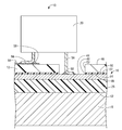
一方、プリント基板12は、図2に示されているように、バスバー回路体16を構成する上層の絶縁体層22と略同一の形状とされており、バスバー回路体16の露呈部44に対応する位置に貫通孔52が形成されている。これにより、プリント基板12の実装面46にバスバー14の上面の一部が露呈されるようになっている。そして、図7に示されているように、このような構造とされた回路構成体10において、プリント基板12のプリント配線54とバスバー回路体16の露呈部44に対して電気部品20の端子部56,56が鉛フリー半田58等を用いたリフロー半田付け等により実装することができるのである。以上のように、プリント基板12のプリント配線54とバスバー回路体16のバスバー14に対して電気部品20をリフロー半田付けにより容易に半田付けすることができことから、製造工程の簡素化を図ることができる。
On the other hand, as shown in FIG. 2, the printed circuit board 12 has substantially the same shape as the upper insulating layer 22 constituting the bus bar circuit body 16, and corresponds to the exposed portion 44 of the bus bar circuit body 16. A through-hole 52 is formed at a position where it does. Thereby, a part of the upper surface of the bus bar 14 is exposed on the mounting surface 46 of the printed circuit board 12. As shown in FIG. 7, in the circuit structure 10 having such a structure, the terminal portion of the electric component 20 with respect to the printed wiring 54 of the printed circuit board 12 and the exposed portion 44 of the bus bar circuit body 16. 56 and 56 can be mounted by reflow soldering using lead-free solder 58 or the like. As described above, since the electrical component 20 can be easily soldered to the printed wiring 54 of the printed circuit board 12 and the bus bar 14 of the bus bar circuit body 16 by reflow soldering, the manufacturing process can be simplified. Can do.
ここで、複数本のバスバー14を仮連結していた図示しないタイバーをカットするタイバーカット工程や、バスバー14の端部を屈曲してヒューズ接続端子部30及びコネクタ接続端子部32を形成する屈曲工程は、本実施形態ではリフロー半田付けの後行われるが、それらの工程をリフロー半田付けの前に行ってもよい。なお、理解を容易にするために、バスバー14は全ての図においてタイバーカットと屈曲加工が完了した形状で示されている。
Here, a tie bar cutting step of cutting a tie bar (not shown) temporarily connecting a plurality of bus bars 14, or a bending step of bending the ends of the bus bar 14 to form the fuse connection terminal portion 30 and the connector connection terminal portion 32. Although this is performed after reflow soldering in this embodiment, these steps may be performed before reflow soldering. For ease of understanding, the bus bar 14 is shown in a shape in which tie bar cutting and bending are completed in all the drawings.
最後に、バスバー回路体16のプリント基板12への重ね合わせ面である上層の絶縁体層22の上面60と反対側の面である下層の絶縁体層26の下面62には、バスバー回路体16の平坦部分よりやや大きな形状とされた金属板製のヒートシンク18が、図示しないエポキシ樹脂などの公知の熱伝導性接着剤により直接固着されている。本実施形態では、一体化された絶縁体層22,26にバスバー14が埋設されていることから、金属板製のヒートシンク18を直接バスバー回路体16に固着することができる。それ故、従来ヒートシンクをバスバー回路体に装着する際に別途準備していた絶縁部材を廃止でき、部品点数の削減、構造の簡素化、製造の容易化を図ることができるようになっている。
Finally, the lower surface 62 of the lower insulating layer 26, which is the surface opposite to the upper surface 60 of the upper insulating layer 22, which is the overlapping surface of the bus bar circuit body 16 on the printed circuit board 12, A heat sink 18 made of a metal plate having a shape slightly larger than the flat portion is directly fixed by a known heat conductive adhesive such as an epoxy resin (not shown). In the present embodiment, since the bus bar 14 is embedded in the integrated insulator layers 22 and 26, the heat sink 18 made of a metal plate can be directly fixed to the bus bar circuit body 16. Therefore, it is possible to eliminate an insulating member separately prepared when the heat sink is attached to the bus bar circuit body, thereby reducing the number of parts, simplifying the structure, and facilitating manufacture.
このような構造とされた本実施形態の回路構成体10によれば、一体化された絶縁体層22,26にバスバー14が埋設された状態で回路構成体10が構成されており、バスバー回路体16の上層の絶縁体層22がプリント基板12に重ね合されて固着手段を構成するクリンチ部36を介して固着されている。従って、電気部品20を半田付けにより実装する際に回路構成体10が加熱されてバスバー14の表面めっきが溶融した場合でも、バスバー回路体16のプリント基板12への固着面を構成する上層の絶縁体層22に対してめっきの溶融は何ら影響を与えず、固着状態が安定して維持される。
According to the circuit structure 10 of this embodiment having such a structure, the circuit structure 10 is configured with the bus bar 14 embedded in the integrated insulator layers 22 and 26, and the bus bar circuit An insulating layer 22 that is an upper layer of the body 16 is superposed on the printed circuit board 12 and fixed through a clinching portion 36 that constitutes a fixing means. Therefore, even when the circuit component 10 is heated and the surface plating of the bus bar 14 is melted when the electrical component 20 is mounted by soldering, the insulation of the upper layer constituting the fixing surface of the bus bar circuit body 16 to the printed circuit board 12 is obtained. The melting of the plating does not affect the body layer 22 at all, and the fixed state is stably maintained.
それ故、半田付け時の加熱温度に応じてバスバー14表面のめっきの種類を変更する必要がなく、バスバー14のめっきの選択自由度が向上する。例えば、回路構成体10に鉛フリー半田58のリフロー半田付けにより電気部品20を実装する場合であっても、鉛フリー半田58の溶融温度よりも溶融温度が低い錫めっきをバスバー14に施すことも可能となるのである。
Therefore, it is not necessary to change the type of plating on the surface of the bus bar 14 according to the heating temperature at the time of soldering, and the degree of freedom in selecting the plating of the bus bar 14 is improved. For example, even when the electrical component 20 is mounted on the circuit structure 10 by reflow soldering of the lead-free solder 58, tin plating having a melting temperature lower than the melting temperature of the lead-free solder 58 may be applied to the bus bar 14. It becomes possible.
加えて、一体化された絶縁体層22,26にバスバー14が埋設されることによりバスバー回路体16が一体的に構成されていることから、バスバー回路体16の取扱性や絶縁性の向上が図られる。
In addition, since the bus bar circuit body 16 is integrally formed by embedding the bus bar 14 in the integrated insulator layers 22 and 26, the handleability and insulation of the bus bar circuit body 16 are improved. Figured.
次に、図8を用いて、本発明の回路構成体10に用いられる固着手段の他の態様について詳述するが、上記実施形態と同様な構造とされた部材および部位については、図中に、上記実施形態と同一の符号を付することにより、それらの詳細な説明を省略する。すなわち、かかる回路構成体64は、固着手段が、バスバー回路体16の上層の絶縁体層22とプリント基板12の実装面46と反対側の面48の間に介在された接着シート66によって構成されている点に関して、上記実施形態と異なる実施形態を示すものである。回路構成体64においても、接着シート66によってバスバー回路体16の上層の絶縁体層22とプリント基板12が固着されていることで、前実施形態の回路構成体10と略同様の構造とすることができるので、同様の効果を得ることができる。
Next, other aspects of the fixing means used in the circuit structure 10 of the present invention will be described in detail with reference to FIG. 8, but members and parts having the same structure as the above embodiment are shown in the figure. The same reference numerals as those in the above embodiment are attached, and detailed description thereof is omitted. That is, in the circuit configuration body 64, the fixing means is configured by the adhesive sheet 66 interposed between the upper insulating layer 22 of the bus bar circuit body 16 and the surface 48 opposite to the mounting surface 46 of the printed circuit board 12. In this regard, an embodiment different from the above embodiment is shown. Also in the circuit structure 64, the upper insulating layer 22 and the printed circuit board 12 are fixed to each other by the adhesive sheet 66, so that the circuit structure 64 has substantially the same structure as the circuit structure 10 of the previous embodiment. Therefore, the same effect can be obtained.
また、バスバー回路体16の上層の絶縁体層22のプリント基板12への当接面の広い範囲を接着シート66を介して安定してプリント基板12の実装面46と反対側の面48に固着することができる。しかも、接着シート66が上層の絶縁体層22に直接接着されておりバスバー14表面のめっき部分から離隔されていることから、バスバー14表面のめっきの溶融による接着力への影響を排除することができ、安定した固着状態を有利に保持できる。
Further, a wide range of the contact surface of the upper insulating layer 22 of the bus bar circuit body 16 to the printed circuit board 12 is stably fixed to the surface 48 opposite to the mounting surface 46 of the printed circuit board 12 through the adhesive sheet 66. can do. In addition, since the adhesive sheet 66 is directly bonded to the upper insulator layer 22 and is separated from the plated portion on the surface of the bus bar 14, the influence on the adhesive force due to melting of the plating on the surface of the bus bar 14 can be eliminated. Can be advantageously maintained in a stable state.
なお、本態様では、クリンチ部36に代えて接着シート66を固着手段として採用した例を示したが、クリンチ部36と接着シート66の両方を固着手段として採用して、プリント基板12とバスバー回路体16の更なる固着安定性を図ってもよい。
In this embodiment, the example in which the adhesive sheet 66 is used as the fixing means instead of the clinching portion 36 is shown. However, both the clinch portion 36 and the adhesive sheet 66 are used as the fixing means, and the printed circuit board 12 and the bus bar circuit Further fixing stability of the body 16 may be achieved.
以上、本発明の実施形態について詳述したが、本発明はその具体的な記載によって限定されない。例えば、固着手段は、バスバー回路体16の上層の絶縁体層22をプリント基板12の実装面46と反対側の面48に相対位置を固定して取り付けられるものであれば何れでもよく、例えば、上層の絶縁体層22とプリント基板12の間に介在される接着剤であってもよく、上層の絶縁体層22とプリント基板12を挟持するボルトとナット等によって構成してもよい。
As mentioned above, although embodiment of this invention was explained in full detail, this invention is not limited by the specific description. For example, the fixing means may be any means as long as the insulator layer 22 on the upper layer of the bus bar circuit body 16 is attached to the surface 48 opposite to the mounting surface 46 of the printed circuit board 12 with its relative position fixed. It may be an adhesive interposed between the upper insulating layer 22 and the printed circuit board 12, or may be constituted by bolts and nuts that sandwich the upper insulating layer 22 and the printed circuit board 12.
また、バスバー回路体16は、例示の如くバスバー14をプリプレグのシートで表裏両面側から挟んで熱圧着する方法の他、バスバー14をインサート品としてバスバー14の周囲に合成樹脂からなる絶縁体層をモールド成形して構成してもよい。
Further, the bus bar circuit body 16 includes a method in which the bus bar 14 is sandwiched from both front and back sides by thermocompression bonding as illustrated, and an insulating layer made of a synthetic resin is provided around the bus bar 14 using the bus bar 14 as an insert. It may be configured by molding.