WO2015045586A1 - 蛍光検出装置及び蛍光検出方法 - Google Patents
蛍光検出装置及び蛍光検出方法 Download PDFInfo
- Publication number
- WO2015045586A1 WO2015045586A1 PCT/JP2014/069194 JP2014069194W WO2015045586A1 WO 2015045586 A1 WO2015045586 A1 WO 2015045586A1 JP 2014069194 W JP2014069194 W JP 2014069194W WO 2015045586 A1 WO2015045586 A1 WO 2015045586A1
- Authority
- WO
- WIPO (PCT)
- Prior art keywords
- light
- fluorescence detection
- detection apparatus
- receiving element
- lens
- Prior art date
- Legal status (The legal status is an assumption and is not a legal conclusion. Google has not performed a legal analysis and makes no representation as to the accuracy of the status listed.)
- Ceased
Links
Images







Classifications
-
- G—PHYSICS
- G01—MEASURING; TESTING
- G01N—INVESTIGATING OR ANALYSING MATERIALS BY DETERMINING THEIR CHEMICAL OR PHYSICAL PROPERTIES
- G01N21/00—Investigating or analysing materials by the use of optical means, i.e. using sub-millimetre waves, infrared, visible or ultraviolet light
- G01N21/62—Systems in which the material investigated is excited whereby it emits light or causes a change in wavelength of the incident light
- G01N21/63—Systems in which the material investigated is excited whereby it emits light or causes a change in wavelength of the incident light optically excited
- G01N21/64—Fluorescence; Phosphorescence
- G01N21/645—Specially adapted constructive features of fluorimeters
-
- G—PHYSICS
- G01—MEASURING; TESTING
- G01N—INVESTIGATING OR ANALYSING MATERIALS BY DETERMINING THEIR CHEMICAL OR PHYSICAL PROPERTIES
- G01N27/00—Investigating or analysing materials by the use of electric, electrochemical, or magnetic means
- G01N27/26—Investigating or analysing materials by the use of electric, electrochemical, or magnetic means by investigating electrochemical variables; by using electrolysis or electrophoresis
- G01N27/416—Systems
- G01N27/447—Systems using electrophoresis
- G01N27/44704—Details; Accessories
- G01N27/44717—Arrangements for investigating the separated zones, e.g. localising zones
- G01N27/44721—Arrangements for investigating the separated zones, e.g. localising zones by optical means
-
- G—PHYSICS
- G01—MEASURING; TESTING
- G01N—INVESTIGATING OR ANALYSING MATERIALS BY DETERMINING THEIR CHEMICAL OR PHYSICAL PROPERTIES
- G01N21/00—Investigating or analysing materials by the use of optical means, i.e. using sub-millimetre waves, infrared, visible or ultraviolet light
- G01N21/62—Systems in which the material investigated is excited whereby it emits light or causes a change in wavelength of the incident light
- G01N21/63—Systems in which the material investigated is excited whereby it emits light or causes a change in wavelength of the incident light optically excited
- G01N21/64—Fluorescence; Phosphorescence
- G01N21/645—Specially adapted constructive features of fluorimeters
- G01N21/6452—Individual samples arranged in a regular 2D-array, e.g. multiwell plates
-
- G—PHYSICS
- G01—MEASURING; TESTING
- G01N—INVESTIGATING OR ANALYSING MATERIALS BY DETERMINING THEIR CHEMICAL OR PHYSICAL PROPERTIES
- G01N2201/00—Features of devices classified in G01N21/00
- G01N2201/06—Illumination; Optics
- G01N2201/064—Stray light conditioning
-
- G—PHYSICS
- G01—MEASURING; TESTING
- G01N—INVESTIGATING OR ANALYSING MATERIALS BY DETERMINING THEIR CHEMICAL OR PHYSICAL PROPERTIES
- G01N27/00—Investigating or analysing materials by the use of electric, electrochemical, or magnetic means
- G01N27/26—Investigating or analysing materials by the use of electric, electrochemical, or magnetic means by investigating electrochemical variables; by using electrolysis or electrophoresis
- G01N27/416—Systems
- G01N27/447—Systems using electrophoresis
- G01N27/44704—Details; Accessories
- G01N27/44717—Arrangements for investigating the separated zones, e.g. localising zones
- G01N27/44721—Arrangements for investigating the separated zones, e.g. localising zones by optical means
- G01N27/44726—Arrangements for investigating the separated zones, e.g. localising zones by optical means using specific dyes, markers or binding molecules
Definitions
- the present invention relates to a fluorescence detection apparatus and a fluorescence detection method using a single-plate light receiving element.
- Patent Document 1 discloses a method for determining a DAN sequence by detecting a fluorescently labeled DNA fragment with a confocal optical system.
- DNA fragments are labeled with fluorescent dyes having different wavelengths for every four base species (A, G, C, T). After injecting this DNA fragment into a glass capillary, voltage is applied to both ends of the capillary for electrophoresis. DNA fragments are separated by the difference in length by electrophoresis. The detection point on the capillary is irradiated with excitation light, and the fluorescence from the DNA fragments separated by electrophoresis is separated by four dichroic mirrors and divided into four optical paths. Then, the color intensity is identified by detecting the fluorescence intensity of one color for each of the four separated light beams using four photo sensors.
- a confocal optical system provided with a pinhole is used in front of the photosensor.
- the plurality of capillaries can be measured by scanning the relative positions of the capillaries with respect to the excitation light.
- the position on the DNA base sequence is identified from the capillary migration time, and the base species is identified from the identified color, and the sequence information of the DNA fragment has been successfully decoded.
- Patent Document 2 discloses a method for acquiring an image of a printed matter using a pinhole array and a color camera. Each pinhole is arranged so that the light imaged on the color camera does not overlap each other.
- Patent Document 3 discloses a method for acquiring spectral information of a subject with high accuracy. In Patent Document 3, light from a subject is divided into two by a half mirror, and one of the two divided lights is used to acquire an image by a color camera, and the other is transmitted through a pinhole. Used to acquire spectrum information with a spectrum sensor. Pinholes are used to limit the viewing field range.
- the spectrum sensor is composed of a photosensor having a plurality of filters that transmit different colors. The bands to be transmitted are all different for each filter, and the spectrum band to be acquired is covered.
- a confocal optical system using a pinhole is an effective method for reducing the influence of background light.
- the technique of Patent Document 1 is an example in which fluorescence is spectrally detected with high sensitivity.
- the optical path length becomes long, and the apparatus is downsized and reduced. It cannot be priced.
- scanning is performed by moving the capillary array in order to measure fluorescence from a plurality of capillaries, which is not desirable from the viewpoint of the stability of the apparatus.
- Patent Document 2 since the image is formed using only the pinhole, the apparatus has a small device configuration. However, since the condenser lens is not used, the amount of fluorescence obtained by the detector is It is weak and the sensitivity cannot be improved. Furthermore, although the technology of Patent Document 3 includes a spectrum sensor that obtains spectrum information, since there is only one photosensor corresponding to each color in the sensor, the fluorescence intensity obtained varies depending on the position of the photosensor. However, the color determination accuracy is not stable. In addition, it takes time to adjust the optical axis to maximize the amount of light irradiated to the photosensors of each color. Furthermore, since there is a need to increase the number of sensors when there are a plurality of detection points, the apparatus becomes large.
- An object of the present invention is to provide an inexpensive and compact fluorescence detection apparatus that reduces autofluorescence from a chip material.
- the present inventors have received the light passing through the pinhole in the confocal optical system with a single-plate light receiving element provided at a position deviating from the focal position, and measuring the amount of light for each color. Has found that can be solved.
- the present application includes a plurality of means for solving the above-described problems.
- a lens that collects light from at least one measurement object held on a substrate, a light receiver that measures the light, A light shielding plate facing the light receiving element between the light receiver and the lens and disposed at a focal position of the lens, the light shielding plate having at least one pinhole, and the light receiver
- a single-plate light-receiving element disposed at a position off the focal point of the lens, and the single-plate light-receiving element has a plurality of pixel groups each having a plurality of color pixels as a unit
- the fluorescence detector is provided in which the light receiver receives the light passing through the pinhole by the light receiving element.
- the step of condensing light from at least one measurement object held on the substrate by the lens, and at least one pinhole are disposed at the focal position of the lens.
- a light receiving device including a step of shielding the light by a light shielding plate and a single plate light receiving element arranged at a position off the focal point of the lens, the light passing through the pinhole is caused by the light receiving element.
- the single-plate light receiving element includes a plurality of pixel groups each including a plurality of color pixels as a unit.
- FIG. 1A is a configuration example of a chip electrophoresis apparatus (fluorescence detection apparatus) in the present embodiment.
- a chip electrophoresis apparatus after injecting a sample solution into a flow path formed on a substrate, a voltage is applied to both ends to perform electrophoresis, so that the mobility of the sample solution component is based on charge, size, shape, etc.
- the sample components are detected by the detector.
- the fluorescence detection apparatus includes an optical system 101, an electrophoresis chip 130, a power source 136, a control unit 140, a temperature control unit 150, and a color camera 120.
- the power source 136 is used to apply a voltage to the chip channels 134 a to 134 d in the electrophoresis chip 130.
- the temperature adjustment unit 150 is used to keep the temperature of the chip channels 134a to 134d constant.
- the optical system 101 is used to excite a dye modified with a DNA fragment separated by electrophoresis and detect the fluorescence 103.
- the color camera 120 measures the light quantity of the pixel corresponding to the color for the light that has passed through the pinhole 104 described below.
- the power source 136, the temperature control unit 150, and the optical system 101 are automatically controlled by the control unit 140.
- the control unit 140 has a function of analyzing signal data from the color camera 120 and converting it into DNA sequence information.
- FIG. 1A shows a cross-sectional view of the electrophoresis chip
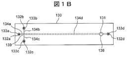
- FIG. 1B shows a top view of the electrophoresis chip.
- the electrophoresis chip 130 is manufactured by bonding a chip body 135a and a chip film 135b.
- the chip body 135a is provided with grooves for forming the flow paths 134a to 134d and wells 133a to 133d for holding the solution.
- a plurality of sets of wells 133a-133d and flow paths 134a-134d may be provided in the same chip.
- the flow paths 134a-134d are formed in the electrophoresis chip 130.
- the material of the chip film 135b is not particularly limited, but the same material or the same resin as that of the chip body 135a is preferable.
- the material of the electrophoresis chip 130 is preferably a resin with less background light, such as an acrylic resin or a cycloolefin resin.
- the electrophoresis chip 130 includes a main body of cycloolefin resin or polymethacryl methacrylate resin and a film of the resin.
- the thickness of the chip body 135a is not particularly limited, but is, for example, 1 mm. Although the thickness of the chip film 135b to be bonded is not particularly limited, the thickness is preferably as thin as possible to reduce background light. The thickness of the chip film 135b is desirably 1 mm or less, for example, 0.1 mm. In addition, since the chip film 135b is thin, it is easy to adjust the temperature in the flow paths 134a to 134d, and there is an effect of improving the degree of separation of the detection target (DNA fragment in this embodiment) by electrophoresis.
- a detection recess 138 may be provided in the chip body 135a.
- the detection recess 138 is formed by reducing the thickness of the chip body 135a in the vicinity of the fluorescence detection point 131. Since the detection depression 138 is present, the background light intensity of the resin can be reduced as compared with the case where there is no detection depression 138, so that the sensitivity (S / N ratio) of fluorescence detection is improved.
- the “SN ratio” means the ratio of the fluorescence signal detected with respect to the noise generated in the color camera 120.
- the effect of using the detection dent 138 is also exhibited when another optical system other than the optical system of the present embodiment is used.
- “Noise” is a standard deviation of the detection intensity detected by the color camera 120 when the fluorescent signal is not detected, that is, the background light intensity.
- the “fluorescence signal” is obtained by subtracting the background light intensity from the fluorescence 103 intensity detected by the color camera 120. That is, the “fluorescence signal” is ideally a signal intensity due to only fluorescence emitted from the detection target. Light other than fluorescence (such as resin-derived Raman scattered light) excited by the excitation light 102 becomes background light.
- the electrophoresis chip 130 as described above is produced by, for example, injection molding.
- the cross-sectional shape of the flow paths 134a to 134d is not particularly limited, but is a square having a width of 0.05 mm and a depth of 0.05 mm, for example.
- the lengths of the flow paths A, B, and C (134a to 134c) are 5 mm each, and the length of the flow path D (134d) is 105 mm.
- the irradiation and detection position on the flow path is on the flow path D (134d), for example, 5 mm away from the well D (133d).
- the shape of each well 133a-133d is, for example, a cylinder having a diameter of 2 mm.
- the cross-sectional shapes of the wells 133a-133d and the flow paths 134a-134d may be other shapes.
- the heat insulating sheet 137 may be brought into close contact with the upper surface of the chip body 135a, or a sheet having good thermal conductivity may be inserted between the chip body 135a and the heat insulating sheet 137. Electrodes 132a-132d are inserted into the wells 133a-133d, respectively, and the electrodes 132a-132d are connected to the power source 136.
- the optical system 101 includes a light source 105, an excitation light condensing lens 107, an objective lens 110, an excitation light cut filter 108, a tube lens 106, and a pinhole 104 (for example, a light shield having a pinhole). Board).
- the configuration of the optical system 101 will be described below along the path along which light travels.
- the excitation light 102 emitted from the light source 105 is condensed at the detection point 131 on the flow path D (134d) by the excitation light condensing lens 107.
- the condensed light is irradiated to the four kinds of phosphors modified with the DNA fragments, and thereby the fluorescence 103 is excited.
- BigDye TM registered trademark: Life Technologies
- As the light source 105 a laser oscillating at 505 nm was used.
- the light emitted from the detection point 131 including the fluorescence 103 is converted into a parallel light beam by the objective lens 110, and then the excitation light scattering component is removed by the excitation light cut filter.
- the fluorescence 103 that has passed through the cut filter 108 is collected by the tube lens 106 and forms an image on the surface on which the pinhole 104 is disposed.
- a camera lens having an NA of 0.4 and a focal length of 35 mm was used for the objective lens 110 and the tube lens 106, and the light emitted from the detection point 131 was imaged at the same magnification at the position of the pinhole 104.
- a microscope objective lens may be used as the objective lens 110.
- a long-pass filter that removes light of 520 nm or less was used as the excitation light cut filter 108.
- the hole diameter of the pinhole 104 is not particularly limited, but is 50 um, for example.
- the pinhole 104 faces the color camera 120 between the color camera 120 and the tube lens 106 and is installed at the focal position of the tube lens 106. Light emitted from a position out of the focus of the objective lens 110 is blocked without passing through the pinhole 104. The light intensity of the light passing through the pinhole 104 is detected by the color camera 120 installed immediately after.
- S / N ratio high fluorescence detection sensitivity
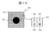
- the color camera 120 includes a single-plate light receiving element 121.
- the light receiving element 121 is an aggregate of pixel groups 126 arranged in an array.
- One pixel group 126 includes a plurality of pixels (122 to 125) arranged in an array.
- the pixel (122-125) includes a filter that transmits a specific color and a photosensor that detects the transmitted light. The filter covers the photosensor, and only the light transmitted through the filter is detected by the photosensor.
- the shape of the pixel (122-125) is not particularly limited, but is, for example, a square having a side of 24 um.
- the example of four (that is, four colors) filter types of the pixel (122-125) is shown, but two or more types may be used. There may be a plurality of filters of the same type in the pixel group 126.
- the transmittance characteristic of the filter is designed so that the color of the fluorescent material transmitted by one type of filter is one color, but a plurality of colors may be transmitted.
- single plate means that there is only one light receiving element in the color camera device.
- the light receiving element 121 of the color camera 120 is installed at a position out of the focus of the tube lens 106. Therefore, the spot (light beam) 127 of the fluorescence 103 on the light receiving element 121 becomes a blurred image than the image formed on the pinhole 104 (FIG. 1C).
- the diameter of the spot 127 on the light receiving element 121 can be adjusted by the distance between the pinhole 104 and the light receiving element 121.
- the spot 127 includes a plurality of pixel groups 126 (that is, a plurality of pixels (122-125) of each color are included).
- the spot 127 has the intensity distribution of the fluorescence 103, there arises a problem that the intensity of the fluorescence 103 varies depending on the position of the pixel.
- a fluorescence signal per color can be calculated as an integrated value of a plurality of pixels of the same color. , Variation in light incident on the pixels of each color can be reduced. Thereby, the determination accuracy of the color of the phosphor can be improved.
- the spot 127 of the fluorescence 103 is made to be an image that is more blurred than the image formed on the pinhole 104 and is detected by a plurality of pixels for each color. Variation in light incident on the pixels can be reduced.
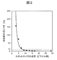
- FIG. 2 shows the result of calculating the variation (CV value) between the four colors of the light intensity incident on the pixel (122-125) with respect to the diameter of the light spot 127.
- the light intensity distribution in the light spot 127 is assumed to follow a normal distribution, and the diameter of the pixel (122-125) included within 6 times the standard deviation of the intensity distribution is defined as the diameter of the spot 127.
- the intensity variation is a CV value obtained by integrating the fluorescence signals of the respective color pixels (122 to 125) in the minimum square region including the spot 127. At this time, the unit constituting the square is the pixel group 126.
- the variation in the light intensity of each color decreased as the diameter of the spot 127 increased.
- the optical system of the present embodiment is an equal magnification imaging, and the imaging size of the detection point 131 is about 50 ⁇ m. Since the pixel size of the light receiving element 121 is 24 um, the diameter of this imaging size corresponds to 2 pixels.
- the result of FIG. 2 shows that the light intensity variation can be drastically reduced by making the diameter of the spot 127 larger than 2 pixels, specifically by making the diameter 3 pixels or more.
- the number of pixels (122-125) of each color included in the spot 127 is two or more.
- the spot 127 is detected in order to detect four colors.
- the diameter of each should be 4 pixels or more. Furthermore, when the diameter is 8 pixels or more, the CV value is 10% or less, and the uniformity of the amount of light incident on the pixels (122-125) of each color is maintained, so that the color determination accuracy is further stabilized.
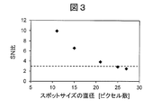
- FIG. 3 is an example of the SN ratio when the diameter of the spot 127 is changed.
- the fluorescence signal and noise per pixel when the diameter of the spot 127 changed was calculated, and the average value of the S / N ratio was obtained for each color in the smallest square area where one side included the spot 127.
- the lowest value in the S / N ratio of the four colors was adopted as the value in FIG.
- the S / N ratio decreases with the diameter of the spot 127.
- the color can be determined if the diameter of the spot 127 is 20 pixels or less.
- the larger the SN ratio the more stable the color determination accuracy.
- the color determination accuracy is stabilized by selecting the diameter of the spot 127 that is larger than the above condition of the uniformity of the light quantity and has a sufficiently large S / N ratio.
- the distance between the pinhole 104 and the light receiving element 121 is about 0.5 mm, so that the diameter of the spot 127 is 10 pixels (240 um).
- the distance of the color camera 120 to the pinhole 104 is adjusted so that the spot 127 is within the range of 8 ⁇ 8 pixels or more and 20 ⁇ 20 pixels or less on the light receiving element 121. The range is acceptable.
- the pixels are accumulated for each color within the square area, but may be accumulated within areas of other shapes such as a circle and a rectangle. Further, instead of the integrated value for each color, the average value of the pixels for each color may be calculated.
- the temperature control unit 150 is disposed on the side surface of the chip film 135b. Keeping the temperature of the flow paths 134a to 134d constant by the temperature controller 150 has an effect of keeping the electrophoresis time and the separation degree of nucleic acids by electrophoresis constant. In this embodiment, for example, the temperature is 50 degrees.
- the temperature control unit 150 has a structure in which a temperature adjusting mechanism and a temperature sensor are incorporated into a plate having an area of 100 mm ⁇ 120 mm and a thickness of 10 mm.
- the temperature sensor measures the temperature of the lower surface of the electrophoresis chip 130 and transmits temperature data to the control unit 140.
- the controller 140 drives the temperature adjustment mechanism based on the received temperature data to keep the temperature of the electrophoresis chip 130 constant.
- the temperature adjusting mechanism may be air cooled by blowing air with a fan, or may be cooled by water by contacting piping. Although a thermocouple is used as the temperature sensor, other sensors may be used.
- the plate of the temperature control unit 150 is preferably a metal such as aluminum, brass, copper, or iron, and any material other than metal that has high thermal conductivity may be used.
- the metal plate may be provided with a fin structure for heat dissipation.
- the temperature control efficiency is better when the temperature control unit 150 and the chip film 135b are in close contact with each other. If there is a gap between the temperature control unit 150 and the chip film 135b, an air layer exists, and the heat conduction efficiency decreases.
- the electrophoresis chip 130 may be pressed against the temperature control unit 150 with a fixing jig such as a clamp.
- the heat insulating sheet 137 may be in close contact with the upper surface of the electrophoresis chip 130, or a sheet having good thermal conductivity may be inserted between the electrophoresis chip 130 and the heat insulating sheet 137. Adhering the heat insulating sheet 137 to the upper surface of the chip has an effect of maintaining temperature uniformity in the flow paths 134a to 134d.
- a silicon sheet as a sheet having good thermal conductivity.
- the heat insulating sheet 137 there is a polystyrene sheet.
- a material that easily deforms and has high thermal conductivity such as a heat conductive sheet or silicon rubber, may be filled between the temperature control unit 150 and the chip film 135b.
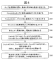
- FIG. 4 is a flowchart of a nucleic acid sequencing method.
- the Sanger method used in capillary sequencers was used for this method.
- a cross-injection method was used to inject the DNA sample into the chip channel (Shi, Electrophoresis, 27, 3703, 2006). The specific method is described below.
- the electrophoresis chip 130 is placed on the temperature control unit 150, and the temperature of the temperature control unit 150 is set to the temperature (50 degrees) at the time of measurement (201).
- the electrophoresis polymer is filled from well D (133d) at a pressure of about 0.5 MPa (202).
- a 4% wt linear polyacrylamide aqueous solution was used as the polymer.
- a buffer solution (1 ⁇ TTE: 50 mM Tris, 50 mM TAPS, 20 mM EDTA) having the same composition as the electrophoresis polymer is injected into well A (133a), well B (133b), and well D (133d) (203).
- a solution (DNA sample) modified with the four types of phosphors and containing DNA fragments of different lengths is injected into the well C (133c) (204).
- the modification is performed by, for example, a cycle sequence using a commercially available kit (for example, BigDye (registered trademark) Terminator v3.1 Cycle Sequencing kit manufactured by Life Technologies).
- electrodes 132a-132d are inserted into the respective wells 133a-133d, and the electrodes 132a-132d are brought into electrical contact with the solution (205).
- a sample is injected into the paths B and C (134b, 134c) (206).
- Vc 0V is applied to the well A (133a)
- Vd 220V is applied to the wells B and C (133b, 133c)
- Ve 3300V is applied to the well D (133d).
- data detection by the light receiving element 121 of the color camera 120 is started (207).
- the data capture interval is 10 Hz
- the exposure time is 60 milliseconds
- 10 ⁇ 10 pixel areas (25 pixels for each color) included in the spot 127 are integrated. Calculation of the fetched data is performed by the control unit 140.
- the control unit 140 integrates the signal intensities of the pixels included in the region included in the spot 127 for each color, and refers to the reference matrix to determine the color of the phosphor detected for each electrophoresis time.
- the reference matrix is a ratio of fluorescence signal intensities at which each color is detected by various pixels. In this embodiment, since four types of phosphors are used, the reference matrix is a 4 ⁇ 4 matrix. Using the inverse matrix of the reference matrix, the fluorescence signal intensity ratio detected at each pixel is converted into the fluorescence signal intensity of each phosphor. Such a reference matrix is acquired by calibration described later. In this example, 500 bases were decoded in 23 minutes. After a certain period of time, the device automatically stops.
- the inside of the flow paths 134a to 134d of the chip may be treated with a coating agent before electrophoresis.
- the coating agent include polydimethylacrylamide / diethylacrylamide (Shi, Electrophoresis, 27, 3703, 2006).
- the electrophoresis may be started after being left for a certain period of time.
- preliminary electrophoresis may be performed by applying a voltage before injecting the nucleic acid.
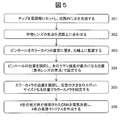
- FIG. 5 is a flowchart showing a calibration procedure.
- the flow paths 134a to 134d are filled with water (301).
- the solution to be filled may be a solution containing water such as a migration polymer or a buffer.
- the focus of the objective lens 110 is adjusted to the detection point 131 on the flow path D (134d) (302).
- the pinhole 104 is placed on the optical path, and the color camera 120 is placed immediately after the pinhole 104 (303).
- the pinhole 104 and the color camera 120 are moved back and forth with respect to the optical axis direction and finely adjusted at the same time, and the pinhole 104 is fixed at a position where the Raman scattered light intensity of water is the highest (304).
- the position of the color camera 120 is fixed at a position where a desired spot 127 size can be obtained by moving the color camera 120 back and forth to adjust the position (305). Thereby, the integration range of the pixel corresponding to the detection point 131 on the flow path D (134d) is determined.
- the standard sample is electrophoresed to create a reference matrix (306).
- the standard sample is a sample in which the four color phosphors are modified with DNA having different chain lengths. Since the order of the colors of the phosphors detected by electrophoresis is known, the ratio of the fluorescence signal intensities of the four color pixels (122-125) is obtained for each phosphor.
- a 4 ⁇ 4 matrix in which such four signal intensity ratios are arranged for the four types of phosphors is a reference matrix.
- a position adjustment and fixing mechanism may be provided.
- the above calibration is performed before shipping the apparatus, but may be performed every time the chip is replaced. It is desirable to confirm the position on the flow path D (134d) and the diameter of the spot 127 every time the electrophoresis chip 130 is replaced. It is necessary to create the reference matrix when changing the type of phosphor or when replacing the light source 105.
- the electrophoresis chip 130 is provided with a plurality of flow paths. This has the effect of improving the number of samples processed in parallel. Note that the description of the components denoted by the same reference numerals as in FIGS. 1A to 1C is omitted.
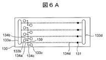
- FIG. 6A is an example of the electrophoresis chip 130 provided with four sets of wells 133a-133d and flow paths 134a-134d.
- the four sets of flow paths 134a to 134d share the wells 133a and 133d, and the wells 133b and 133c are provided in the four sets of flow paths 134a to 134d, respectively.
- a detection point 131 is provided for each flow path 134d.
- FIG. 6B is an example of the optical system 101 of the chip electrophoresis apparatus in the present embodiment.
- a pinhole array 1041 for example, a light shielding plate having a plurality of pinholes
- the same number of pinholes as the detection points 131 is installed.
- Fluorescence 103 from a plurality of detection points 131 is converted into a parallel light beam by one objective lens 110 and imaged on a pinhole array 1041 by one tube lens 106.
- the imaging points of the four detection points 131 and the positions of the pinholes are made to coincide with each other.
- fluorescence signals from a plurality of detection points 131 can be detected simultaneously by one color camera 120.
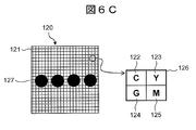
- FIG. 6C is a diagram showing a color camera and spots on the color camera.
- a plurality of spots 127 from the detection points 131 on the light receiving element 121 are arranged in a line.
- the size of each spot 127 in this embodiment needs to take into account the light uniformity and the SN ratio.
- the optical system 101 forms an equal-magnification image, it is necessary to make the interval between the flow paths D (134d) larger than the diameter of the spot 127.
- all the spots 127 are included in the light receiving element 121. According to the configuration of the present embodiment, it is not necessary to increase the number of optical components such as detectors and lenses, the apparatus can be reduced in size and price, and the adjustment of the optical system 101 is simplified.
- This embodiment is characterized in that a plurality of detection points 131 are alternately shifted in the flow path direction. Thereby, the interval between the flow paths D (134d) in the electrophoresis chip 130 can be reduced, and the electrophoresis chip 130 can be downsized. It should be noted that the description of the components denoted by the same reference numerals as in FIGS. 1A to 1C and FIGS. 6A to 6C is omitted.
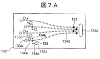
- FIG. 7A is an example of the electrophoresis chip 130 in which the detection points 131 on the adjacent flow paths D (134d) are alternately shifted in the flow path direction.
- a plurality of detection points 131 are arranged by changing the distance from the well D (133d) to the detection point 131 for each flow path D (134d).
- the migration distance from the intersection 139 of the channels 134a to 134d to the detection point 131 is the same for all channels.
- FIG. 7B is an example of the optical system 101 of the chip electrophoresis apparatus in the present embodiment.
- the position of each pinhole in the pinhole array 1041 is arranged corresponding to the detection point 131.
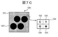
- FIG. 7C is a diagram illustrating a color camera and spots on the color camera. A plurality of spots 127 from the detection points 131 on the light receiving element 121 are arranged in two rows and shifted from each other.
- the distance between the flow paths D (134d) needs to be larger than the diameter of the spot 127.
- the arrangement of the detection points 131 of this embodiment is not limited. According to this, it becomes possible to make the space
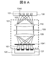
- FIG. 8A shows an example of the optical system 101 in which the microlens 161 is arranged immediately after the pinhole array 1041.
- FIG. 8B is a diagram showing a color camera and spots on the color camera in the configuration of FIG. 8A. Since the spread angle of the light passing through the microlens 161 becomes small, the size of the plurality of spots 127 from the detection point 131 on the light receiving element 121 can be adjusted.
- the distance from the pinhole array 1041 to the light receiving element 121 can be taken. Since the amount of change in the size of the spot 127 on the light receiving element 121 is reduced, the calibration (305) for confirming the position of the spot 127 becomes easier.
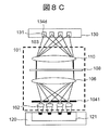
- FIG. 8C shows an example of the optical system 101 in which the micro cylindrical lens 162 is arranged immediately after the pinhole array 1041.
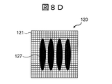
- FIG. 8D is a diagram showing a color camera and spots on the color camera in the configuration of FIG. 8C.
- the micro cylindrical lens 162 is installed immediately after the pinhole array 1041.
- the spot 127 formed on the light receiving element 121 by the light passing through the micro cylindrical lens 162 has an elliptical shape, and is arranged so that the major axes of the spots 127 are parallel to each other. With this arrangement, the distance between the spots 127 can be reduced while ensuring the size of the spots 127, and the electrophoresis chip 130 can be downsized.
- a rod lens may be used to irradiate an elongated line.
- a pinhole array 1041 provided in a two-dimensional lattice shape is used.
- fluorescence measurement can be performed on a sample that is two-dimensionally arranged in a grid (arrayed). It should be noted that the description of the components denoted by the same reference numerals as in FIGS. 1A to 1C and FIGS. 6A to 6C is omitted.
- FIG. 9A is a configuration example of the fluorescence detection system of the chip electrophoresis apparatus in the present example.
- FIG. 9B is a configuration example of a microarray in which detection points are two-dimensionally arranged in the present embodiment.
- the microarray 171 has a large number of DNA fragments arranged on a substrate such as plastic or glass at a high density.
- a plurality of detection points 131 are two-dimensionally arrayed.
- a single-stranded DNA having a known base sequence is immobilized at each detection point 131, and each detection point 131 has a different base sequence.
- the DNA to be measured is modified with a phosphor. In the case of multiple samples, the phosphors of different colors are modified.
- the pinhole array 1041 has holes at the imaging positions of the detection points 131 to be measured at a time, and is installed immediately before the light receiving element 121.
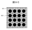
- FIG. 9C is a diagram showing a color camera and spots on the color camera in the present embodiment.
- the plurality of spots 127 on the light receiving element 121 are arranged so as not to overlap each other. Since a plurality of detection points 131 can be measured simultaneously by one measurement, the throughput is improved. Since a plurality of samples capable of discriminating a plurality of colors can be measured simultaneously, there is also an effect that a quantitative comparison between samples can be performed. If the sample is held on a movable table such as an XY stage, more detection points 131 can be scanned, and the measurement efficiency is improved.
- the present invention is not limited to DNA microarrays, and may be used for identifying a plurality of fluorescence using a two-dimensionally arrayed sample. For example, Southern blotting, real-time sequencer (Eid et al., Science, 323, 133, 2009), etc. It can be applied to.
- FIG. 10 shows an example of the configuration of this embodiment.
- the stage 400 is configured to move the color camera 120 along the XYZ axes.
- the configuration other than the stage 400 is the same as that of the second embodiment.
- the definition of the XYZ axes is illustrated in FIG.
- the Y axis is perpendicular to the page.
- the pinhole array 1041 is placed at the focal position of the tube lens 106, and the color camera 120 is located away from the focal position.
- the pinhole array 1041 is removed.
- the spot 127 is adjusted to the position where the signal intensity is the smallest and the Z axis of the stage 400 is moved.
- the position of the light receiving element 121 at this time is the focal position.
- the distance between the spots 127 defined by the distance between the flow paths D (134d) of the electrophoresis chip 130 is used.
- the position of the objective lens 110 and the position of the color camera 120 are adjusted until the distance between the two spots 127 is the same as the width between the flow paths D (134d). repeat. Thereafter, the position of the color camera 120 is moved along the Z axis so that the size of the spot 127 on the light receiving element 121 is adjusted within the range defined in the first embodiment.
- a pinhole array 1041 is placed at the imaging position. The position of the pinhole array 1041 is determined by adjusting so that the intensity of the spot 127 of Raman scattered light of water on the light receiving element 121 is maximized.
- the position of the color camera 120 is determined by moving the XY axes of the stage 400 to adjust the position of the color camera 120 with respect to the position of the pinhole array 1041.
- the XY axes can be adjusted with machine accuracy, and in that case, an XY axis stage is unnecessary.
- the position of the color camera 120 in the XY axis direction is arbitrary as long as the spot 127 is within the light receiving element 121, and fine adjustment is not necessary. This is another effect of the present invention.
- the position of the pinhole array 1041 and the color camera 120 can be easily adjusted by the above operation.
- Raman scattered light of water is used for the light from the detection point 131.
- a standard sample containing a phosphor or other luminescent reagent may be used for the magnification adjustment.
- any light emission image whose distance and size are known in advance may be used.
- the present invention is characterized in that the light passing through the pinhole in the confocal optical system is received by the color camera provided at a position deviated from the focal position, and the amount of light for each color is measured. .
- a confocal optical system By adopting a confocal optical system, autofluorescence from the chip material can be reduced, and an inexpensive and small fluorescence detection apparatus can be provided by detecting with a single plate color camera.
- fluorescence as a blurred image on the detector, a plurality of pixels of each color are included, and the color determination accuracy is improved. Even when there are a plurality of detection points, simultaneous detection is possible without changing the configuration of the optical system.
- this invention is not limited to the Example mentioned above, Various modifications are included.
- the above-described embodiments have been described in detail for easy understanding of the present invention, and are not necessarily limited to those having all the configurations described.
- a part of the configuration of one embodiment may be replaced with the configuration of another embodiment, and the configuration of another embodiment may be added to the configuration of one embodiment.
- each configuration, function, processing unit, and the like of the control unit 140 may be realized by hardware by designing a part or all of them, for example, with an integrated circuit.
- each configuration, function, processing unit, and the like of the control unit 140 may be realized by software by interpreting and executing a program that realizes each function by the processor.
- Information such as programs, tables, and files that realize each function can be stored in a storage device such as a memory, a hard disk, or an SSD (Solid State Drive), or a recording medium such as an IC card, an SD card, or a DVD.
- control lines and information lines are those that are considered necessary for the explanation, and not all the control lines and information lines on the product are necessarily shown. Actually, it may be considered that almost all the components are connected to each other.
Landscapes
- Health & Medical Sciences (AREA)
- Life Sciences & Earth Sciences (AREA)
- Chemical & Material Sciences (AREA)
- Physics & Mathematics (AREA)
- Molecular Biology (AREA)
- Analytical Chemistry (AREA)
- Biochemistry (AREA)
- General Health & Medical Sciences (AREA)
- General Physics & Mathematics (AREA)
- Immunology (AREA)
- Pathology (AREA)
- Chemical Kinetics & Catalysis (AREA)
- Electrochemistry (AREA)
- Nuclear Medicine, Radiotherapy & Molecular Imaging (AREA)
- Investigating, Analyzing Materials By Fluorescence Or Luminescence (AREA)
Abstract
蛍光検出装置は、基板に保持された少なくとも1つの測定対象からの光を集光するレンズと、前記光を測定する受光器と、前記受光器と前記レンズの間で前記受光素子に対面し、前記レンズの焦点位置に配置された遮光板と、を備える。前記遮光板は、少なくとも1つのピンホールを有し、前記受光器は、前記レンズの焦点から外れた位置に配置された単板の受光素子を備える。前記単板の受光素子には、複数の色の画素を1単位とする画素群が複数個配列されている。前記受光器は、前記ピンホールを通った前記光を前記受光素子によって受光する。
Description
本発明は、単板の受光素子を用いる蛍光検出装置及び蛍光検出方法に関する。
光を利用した検出では、意図しない背景光を低減し、測定感度を向上させるため、ピンホールを用いた光学系が利用されている。特許文献1では、蛍光標識されたDNA断片を共焦点光学系で検出して、DAN配列を決定する方法を開示している。
特許文献1において、DNA断片は4塩基種(A,G,C,T)ごとに、波長の異なる蛍光色素で標識されている。このDNA断片をガラスキャピラリに注入した後、キャピラリ両端に電圧を印加して電気泳動する。電気泳動によりDNA断片は長さの違いで分離される。キャピラリ上の検出点に励起光を照射して、電気泳動で分離されたDNA断片からの蛍光を、4つのダイクロイックミラーで分光して4つの光路に分ける。そして、4つの分光された光を4つのフォトセンサで1つあたり1色の蛍光強度を検出して色を識別する。ここで、フォトセンサの前にはピンホールが設置された共焦点光学系が用いられている。これにより、キャピラリ表面での励起光の散乱等の背景光を除去している。複数のキャピラリは、励起光に対してキャピラリの相対位置をスキャンすることで測定可能となっている。キャピラリの泳動時間からDNA塩基配列上の位置を、識別された色から塩基種を同定して、DNA断片の配列情報の解読に成功している。
特許文献2は、ピンホールアレイとカラーカメラを使用して、印刷物の画像を取得する方法を開示している。各ピンホールは、カラーカメラ上で結像した光が互いに重ならないように配置されている。また、特許文献3は、被写体のスペクトル情報を高精度に取得する方法を開示している。特許文献3において、被写体からの光はハーフミラーで2つに分けられ、2つに分けられた光の一方はカラーカメラで画像を取得するために用いられ、もう一方はピンホールを透過した後、スペクトルセンサでスペクトル情報を取得するために用いられる。ピンホールは観察視野範囲を限定するために用いられている。スペクトルセンサは、異なる色を透過させる複数のフィルタを備えたフォトセンサで構成されている。透過させる帯域はフィルタごとにすべて異なっており、取得したいスペクトル帯域がカバーされている。
樹脂製マイクロチップと蛍光検出を組み合わせた分析装置では、励起光をマイクロチップに照射したとき、チップ材質からの背景光が大きいために、検出対象からの蛍光信号を良好な信号ノイズ比(SN比)で検出することが困難であった。特に検出対象が微量の場合は、蛍光が微弱になるため、背景光に埋もれてしまう。このような背景光には、チップ材質の自家蛍光やラマン散乱光などがある。
背景光の影響を低減する方法としてピンホールを用いた共焦点光学系は有効な方法である。特許文献1の技術は、高感度に蛍光を分光して蛍光を検出した例であるが、3枚のダイクロイックミラーで4色を分離するために、光路長が長くなって装置の小型化および低価格化ができない。また、複数のキャピラリからの蛍光を測定するためにキャピラリアレイを動かしてスキャンしているが、装置の安定性の点から望ましくない。
また、特許文献2の技術では、ピンホールのみを使用して結像しているため、小型な装置構成となっているが、集光レンズを用いていないために検出器で得られる蛍光量は微弱であり、感度は向上できない。さらに、特許文献3の技術では、スペクトル情報を得るスペクトルセンサを備えているが、センサ中の各色に対応するフォトセンサがそれぞれ1つのみであるため、フォトセンサの位置によって得られる蛍光強度が変動し、色判定精度が安定しない。また、各色のフォトセンサに照射される光量を最大にするための光軸調整に手間がかかる。さらに、複数個の検出点がある場合には上記センサを増やす必要があるため、装置が大型になる。
本発明は、チップ材料からの自家蛍光を低減し、かつ安価で小型な蛍光検出装置を提供することを目的とする。
本発明者らは、共焦点光学系におけるピンホールを通った光を、焦点位置から外れた位置に設けられた単板の受光素子で受光し、色毎の光量を測定することにより、上記課題が解決できることを見出した。
上記課題を解決する為に例えば請求の範囲に記載の構成を採用する。本願は上記課題を解決する手段を複数含んでいるがその一例をあげるならば、基板に保持された少なくとも1つの測定対象からの光を集光するレンズと、前記光を測定する受光器と、前記受光器と前記レンズの間で前記受光素子に対面し、前記レンズの焦点位置に配置された遮光板と、を備え、前記遮光板は、少なくとも1つのピンホールを有し、前記受光器は、前記レンズの焦点から外れた位置に配置された単板の受光素子を備え、前記単板の受光素子には、複数の色の画素を1単位とする画素群が複数個配列されており、前記受光器は、前記ピンホールを通った前記光を前記受光素子によって受光する、蛍光検出装置が提供される。
また、他の例によれば、レンズによって、基板に保持された少なくとも1つの測定対象からの光を集光するステップと、少なくとも1つのピンホールを有し、前記レンズの焦点位置に配置された遮光板によって、前記光を遮光するステップと、前記レンズの焦点から外れた位置に配置された単板の受光素子を備える受光器を用いて、前記ピンホールを通った前記光を前記受光素子によって受光するステップであって、前記単板の受光素子には、複数の色の画素を1単位とする画素群が複数個配列されている、ステップと、を含む蛍光検出方法が提供される。
本発明によれば、チップ材料からの自家蛍光を低減させ、かつ単板の受光素子で検出することによって安価で小型な蛍光検出装置を提供することができる。
本発明に関連する更なる特徴は本明細書の記述添付図面から明らかになるものである。また上記した以外の課題構成及び効果は以下の実施例の説明により明らかにされる。
本発明に関連する更なる特徴は本明細書の記述添付図面から明らかになるものである。また上記した以外の課題構成及び効果は以下の実施例の説明により明らかにされる。
以下添付図面を参照して本発明の実施例について説明する。なお添付図面は本発明の原理に則った具体的な実施例を示しているがこれらは本発明の理解のためのものであり決して本発明を限定的に解釈するために用いられるものではない。なお、本実施例の形態を説明するための全図において同一機構を有するものは原則として同一の符号を付すようにし、その繰り返しの説明は可能な限り省略するようにしている。
[第1実施例]
図1Aは、本実施例におけるチップ電気泳動装置(蛍光検出装置)の構成例である。チップ電気泳動装置では、基板に作製した流路内に、試料溶液を注入した後、両端に電圧を掛けて電気泳動を行うことにより、試料溶液成分が荷電、大きさ、形などに基づく移動度の差異で分離され、検出器より試料成分の検出を行う。
図1Aは、本実施例におけるチップ電気泳動装置(蛍光検出装置)の構成例である。チップ電気泳動装置では、基板に作製した流路内に、試料溶液を注入した後、両端に電圧を掛けて電気泳動を行うことにより、試料溶液成分が荷電、大きさ、形などに基づく移動度の差異で分離され、検出器より試料成分の検出を行う。
蛍光検出装置は、光学系101と、電気泳動チップ130と、電源136と、制御部140と、温調部150と、カラーカメラ120とを備える。電源136は、電気泳動チップ130内のチップ流路134a-134dに電圧を印加するために用いられる。温調部150は、チップ流路134a-134dの温度を一定に保つために用いられる。光学系101は、電気泳動で分離されたDNA断片に修飾されている色素を励起し、蛍光103を検出するために用いられる。カラーカメラ120は、以下で説明するピンホール104を通過した光について色に対応した画素の光量を測定するものである。電源136と温調部150と光学系101は、制御部140によって自動制御される。加えて、制御部140は、カラーカメラ120からの信号データを解析して、DNA配列情報に変換する機能を有する。以下、蛍光検出装置の各構成要素の詳細を説明する。
電気泳動チップの構造の説明
図1Aは、電気泳動チップの断面図を示しており、図1Bは、電気泳動チップの上面図を示す。電気泳動チップ130は、チップ本体135aとチップフィルム135bを張り合わせて作製される。チップ本体135aには、流路134a-134dを形成するための溝と、溶液を保持するためのウェル133a-133dが設けられている。同一チップ内に複数組のウェル133a-133d及び流路134a-134dが設けられてもよい。チップフィルム135bをチップ本体135aの溝がある側に張り合わせることにより、電気泳動チップ130に流路134a-134dが形成される。チップフィルム135bの材質は特に限定しないが、チップ本体135aと同材質または同系統の樹脂が好ましい。
図1Aは、電気泳動チップの断面図を示しており、図1Bは、電気泳動チップの上面図を示す。電気泳動チップ130は、チップ本体135aとチップフィルム135bを張り合わせて作製される。チップ本体135aには、流路134a-134dを形成するための溝と、溶液を保持するためのウェル133a-133dが設けられている。同一チップ内に複数組のウェル133a-133d及び流路134a-134dが設けられてもよい。チップフィルム135bをチップ本体135aの溝がある側に張り合わせることにより、電気泳動チップ130に流路134a-134dが形成される。チップフィルム135bの材質は特に限定しないが、チップ本体135aと同材質または同系統の樹脂が好ましい。
樹脂チップ材料からの自家蛍光やラマン散乱光などの背景光は蛍光測定のノイズとなる。電気泳動チップ130の材質には、前記背景光の少ない樹脂が望ましく、例えばアクリル樹脂やシクロオレフィン樹脂である。一例として、電気泳動チップ130は、シクロオレフィン系樹脂またはポリメタクリルメタクリレート樹脂の本体と、前記樹脂のフィルムとから構成される。
チップ本体135aの厚みは特に限定しないが、例えば1mmである。張り合わせるチップフィルム135bの厚さは特に限定しないが、背景光低減のために薄いほど良い。チップフィルム135bの厚さは1mm以下が望ましく、例えば0.1mmである。また、チップフィルム135bが薄いことにより、流路134a-134d内の温度調節が容易になり、電気泳動による検出対象(本実施例ではDNA断片)の分離度が向上する効果もある。
また、チップ本体135aに検出窪み138を設けても良い。検出窪み138は、蛍光検出点131近傍の部分におけるチップ本体135aの厚さを薄くすることで形成される。検出窪み138があることで、検出窪み138がない場合に比べて樹脂の背景光強度を低減できるので、蛍光検出の感度(SN比)が向上する。ここで、「SN比」とはカラーカメラ120で発生するノイズに対して検出される蛍光信号の比を意味する。もちろん、本実施例の光学系に以外の他の光学系を用いた場合にも、検出窪み138を用いる効果は発揮される。「ノイズ」は、蛍光信号が検出されていないときに、カラーカメラ120で検出される検出強度、すなわち背景光強度の標準偏差である。一方、「蛍光信号」はカラーカメラ120で検出された蛍光103強度から背景光強度を差し引いたものである。すなわち、「蛍光信号」は、理想的には検出対象から発せられる蛍光のみによる信号強度である。励起光102によって励起される蛍光以外の光(樹脂由来のラマン散乱光など)は背景光となる。上記のような電気泳動チップ130は、例えば射出成型で作成される。
流路134a-134dの断面形状は、特に限定されないが、例えば幅0.05mm、深さ0.05mmの正方形である。流路A、B、C(134a-134c)の長さは各5mmであり、流路D(134d)の長さが105mmである。流路上の照射および検出位置は、例えばウェルD(133d)から5mm離れた流路D(134d)上にある。各ウェル133a-133dの形状は、例えば直径2mmの円柱である。上記ウェル133a-133dや流路134a-134dの断面形状は他の形状でも構わない。
また、チップ本体135aの上面に断熱シート137を密着させても良いし、チップ本体135aと断熱シート137との間に熱伝導性の良いシートを挿入しても良い。各ウェル133a-133dには、それぞれ電極132a-132dを挿し込まれており、各電極132a-132dは、電源136に接続されている。
光学系の説明
光学系101は、光源105と、励起光用集光レンズ107と、対物レンズ110と、励起光カットフィルタ108と、チューブレンズ106と、ピンホール104(例えば、ピンホールを有する遮光板)とを備える。以下に、光が進む経路に沿って光学系101の構成を説明する。
光学系101は、光源105と、励起光用集光レンズ107と、対物レンズ110と、励起光カットフィルタ108と、チューブレンズ106と、ピンホール104(例えば、ピンホールを有する遮光板)とを備える。以下に、光が進む経路に沿って光学系101の構成を説明する。
光源105から発せられる励起光102は、励起光用集光レンズ107によって流路D(134d)上の検出点131に集光される。集光された光は、DNA断片に修飾された4種蛍光体に照射されて、これにより、蛍光103が励起される。本実施例では、4種蛍光体としてBigDyeTM(登録商標:Life Technologies社)を用いたが別の蛍光体でも構わない。光源105には505nmで発振するレーザを用いた。
蛍光103を含む検出点131から発せられる光は、対物レンズ110で平行光束化された後、励起光カットフィルタ108で励起光の散乱成分が取り除かれる。カットフィルタ108を通過した蛍光103は、チューブレンズ106によって集光されて、ピンホール104の配置された面で結像する。対物レンズ110とチューブレンズ106にはNAが0.4、焦点距離35mmのカメラレンズを用い、検出点131からの発光をピンホール104の位置で等倍に結像させた。対物レンズ110には顕微鏡用対物レンズを用いても構わない。励起光カットフィルタ108には520nm以下の光を取り除くロングパスフィルタを用いた。
ピンホール104の穴径は特に限定されないが、例えば50umである。ピンホール104は、カラーカメラ120とチューブレンズ106の間でカラーカメラ120対面し、チューブレンズ106の焦点位置に設置される。対物レンズ110の焦点から外れた位置から発せられる光はピンホール104を透過せずに遮断される。ピンホール104を通過した光は、直後に設置されたカラーカメラ120によってその光強度が検出される。このような共焦点光学系を用いることで、樹脂のラマン散乱等による背景光を低減できるため、高い蛍光検出感度(SN比)を達成できる。
従来では、通常、2次元センサと共焦点光学系で多色検出する場合は、ピンホール104位置に結像し、ピンホール104を透過した光線を、別のレンズで平行光束化し、分光素子で各色に分光し、さらにもう一枚の別のレンズで検出器の受光素子平面に再結像させる。しかしながら、本実施例では、このようなレンズと分光素子による再結像系を用いず、ピンホール104の直後にカラーカメラ120を設置することを特徴とする。これにより、装置の小型化や低価格化、及び光学部品数の低減、さらには、後で述べるように高い色判定精度を達成する効果がある。
図1Cに示すように、カラーカメラ120は、単板の受光素子121を備える。受光素子121はアレイ状に配置された画素群126の集合体である。1つの画素群126は、アレイ状に配置された複数の画素(122-125)によって構成される。ここで、画素(122-125)は、特定の色を透過させるフィルタと、その透過した光を検出するフォトセンサとから構成される。上記フィルタはフォトセンサ上を覆い、このフィルタを透過した光のみが、フォトセンサで検出される。画素(122-125)の形状は特に限定されないが、例えば1辺24umの正方形である。
画素(122-125)のフィルタの種類は4つ(すなわち4色)の例を示したが、2種類以上であればよい。また、画素群126内に同一種のフィルタが複数枚あっても良い。ここでは1種類のフィルタが透過させる蛍光体の色は、1色となるようにフィルタの透過率特性を設計したが、複数色を透過させても構わない。ここで、「単板」とは、受光素子がカラーカメラ装置内に1つしかないことを意味する。
以下、本実施例の効果を説明する。カラーカメラ120の受光素子121はチューブレンズ106の焦点から外れた位置に設置される。したがって、受光素子121上の蛍光103のスポット(光束)127は、ピンホール104上に結像される像よりもぼけた像となる(図1C)。受光素子121上のスポット127の直径は、ピンホール104と受光素子121との間の距離により調整が可能である。スポット127の直径を大きくすることで、スポット127内には複数の画素群126が含まれる(すなわち、各色の画素(122-125)が複数含まれる)ようになる。
スポット127は蛍光103の強度分布を持つため、画素の位置によって蛍光103の強度がばらつく問題が生じる。しかし、本実施例では、色毎に複数の画素で検出することにより、1色あたりの蛍光信号を複数の同色画素の積算値として算出できるため、1画素の蛍光信号から算出する場合に比べて、各色の画素に入射する光のばらつきを低減できる。これにより、蛍光体の色の判定精度を向上できる。
また、受光素子121上に結像させる場合は、スポット127の直径が小さくなるため、各色の蛍光強度がばらついて色判定精度が低下する。これに対して、本実施例では、蛍光103のスポット127を、ピンホール104上に結像される像よりもぼけた像とし、かつ、色毎に複数の画素で検出することにより、各色の画素に入射する光のばらつきを低減できる。
図2は、光のスポット127の直径に対して、画素(122-125)に入射される光強度の4色間ばらつき(CV値)を算出した結果である。ばらつきの算出では、光のスポット127内の光強度分布が正規分布に従うと仮定し、強度分布の標準偏差の6倍以内に含まれる画素(122-125)の直径をスポット127の直径とした。強度のばらつきは、スポット127を内包する最小の正方形領域内の各色の画素(122-125)ごとの蛍光信号を、積算した値のCV値である。このとき、正方形を構成する単位は、画素群126である。
図2に示すように、スポット127の直径が大きくなるにつれ、各色の光強度のばらつきは減少した。本実施例の光学系は等倍結像であり、検出点131の結像サイズは50um程度である。受光素子121の画素サイズは24umであるため、この結像サイズの直径は2画素に相当する。図2の結果は、スポット127の直径を2画素よりも大きくすることによって、具体的には直径を3画素以上にすることによって光強度ばらつきを劇的に減少できることを示している。各色の光強度ばらつきを低減するためには、スポット127に含まれる各色の画素(122-125)はそれぞれ2個以上とすることが望ましく、本実施例では4色の検出を行うため、スポット127の直径を4画素以上とすれば良いことが分かった。さらに、直径を8画素以上とするとCV値が10%以下となり、各色の画素(122-125)に入射する光量の均一性が保たれるため、色判定精度が一層安定する。
一方、光のスポット127が大きくなるにつれ、光の密度が低下するため、1画素当りの蛍光信号は低下し、色判定精度も低下することになる。図3は、スポット127の直径を変化させたときのSN比の例である。スポット127の直径が変化したときの1画素当りの蛍光信号とノイズを計算し、1辺がスポット127を内包する最小の正方形領域内の各色についてSN比の平均値を求めた。図3の値には、4色のSN比で最も低い値を採用した。
図3に示すように、SN比は、スポット127の直径とともに低下している。SN比が3以上で測定可能としたとき、スポット127の直径を20画素以下とすれば色の判定が可能となる。SN比は大きいほど、色判定精度は一層安定する。前記の光量の均一性の条件より大きく、SN比が十分大きいスポット127の直径を選択することで色判定精度が安定する。
本実施例では、ピンホール104と受光素子121の距離を約0.5mmとすることにより、スポット127の直径を10画素(240um)とした。SN比を向上する他の手段として、試料の濃度の増加及び入射光強度の増加、カメラの露光時間の増加などと組み合わせることが有効である。以上より、本実施例では、スポット127が受光素子121上で8×8画素以上、20×20画素以内の範囲に収まるように、ピンホール104に対するカラーカメラ120の距離を調整したが、上記以外の範囲でも構わない。本実施例では、正方形の領域内で各色毎に画素を積算したが、円形や長方形など他の形状の領域内で積算してもよい。また、各色毎の積算値ではなく、各色毎の画素の平均値を計算してもよい。
温調部の説明
図1Aに示すように、温調部150は、チップフィルム135bの側面に配置されている。温調部150で流路134a-134dの温度を一定に保つことで、電気泳動時間や電気泳動による核酸の分離度を一定に保つ効果がある。本実施例では、例えば、上記温度は50度である。
図1Aに示すように、温調部150は、チップフィルム135bの側面に配置されている。温調部150で流路134a-134dの温度を一定に保つことで、電気泳動時間や電気泳動による核酸の分離度を一定に保つ効果がある。本実施例では、例えば、上記温度は50度である。
温調部150は、面積100mm×120mm、厚み10mmの板に温度調製機構と温度センサが組み込まれた構造である。温度センサは、電気泳動チップ130の下面の温度を測定し、制御部140に温度データを送信する。制御部140は、受信した温度データをもとに、温度調整機構を駆動させて電気泳動チップ130の温度を一定に保つ。温度調整機構にはファンで風を吹き付けて空冷したり、配管を接触させて水冷温したりしても構わない。温度センサには熱電対を用いたが他のセンサでも構わない。
温調部150の板としては、アルミ、真鍮、銅や鉄などの金属が好ましく、金属以外でも熱伝導率が高い素材であれば良い。金属板には放熱のためのフィン構造を設けても良い。温調部150とチップフィルム135bは密着している方が温調効率は良い。温調部150とチップフィルム135bとの間に隙間があると空気層が存在し、熱伝導効率が下がる。密着させるために、電気泳動チップ130を温調部150にクランプのような固定治具で押しつけても良い。また、電気泳動チップ130の上面に断熱シート137を密着させても良いし、電気泳動チップ130と断熱シート137の間に熱伝導性の良いシートを挿入しても良い。断熱シート137をチップ上面に密着させることで、流路134a-134d内の温度均一性が保たれる効果がある。熱伝導性の良いシートとしてはシリコンシートがある。断熱シート137としてはポリスチレンシートがある。他に温調部150とチップフィルム135bとの間に熱伝導シートやシリコンゴムなど、容易に変形しかつ熱伝導率の高い素材を満たしてもよい。
核酸の配列決定方法
図4は核酸の配列決定方法のフローチャートである。本法にはキャピラリーシーケンサで用いられるサンガー法を用いた。DNA試料のチップ流路への注入にはクロスインジェクション法を用いた(Shi、 Electrophoresis、 27、 3703、 2006)。以下に具体的な方法を記述する。
図4は核酸の配列決定方法のフローチャートである。本法にはキャピラリーシーケンサで用いられるサンガー法を用いた。DNA試料のチップ流路への注入にはクロスインジェクション法を用いた(Shi、 Electrophoresis、 27、 3703、 2006)。以下に具体的な方法を記述する。
電気泳動チップ130を温調部150に置き、温調部150の温度を測定時の温度(50度)に設定する(201)。ガスタイトシリンジとフェラル、ナット、チューブを使用し、約0.5MPaの圧力でウェルD(133d)から電気泳動用ポリマを充填する(202)。本実施例では、ポリマとして4%wtの直鎖状ポリアクリルアミド水溶液を使用した。
次に、ウェルA(133a)、ウェルB(133b)、ウェルD(133d)に、電気泳動用ポリマと同じ組成を持つバッファ溶液(1xTTE:50mM Tris、 50mM TAPS、 20mM EDTA)を注入する(203)。次に、4種蛍光体で修飾されかつ異なる長さのDNA断片を含む溶液(DNA試料)をウェルC(133c)に注入する(204)。前記修飾は、例えば、市販されているキット(例えばLife Technologies社製のBigDye(登録商標)Terminator v3.1 Cycle Sequencing kit)を用いたサイクルシーケンスにより行われる。
次に、各ウェル133a-133dにそれぞれ電極132a-132dを挿し込み、電極132a-132dを溶液と電気的に接触させる(205)。ウェルA、C、D(133a、133c、133d)にVa=0V、ウェルB(133b)にVb=300V印加し、100秒間電気泳動してウェルC(133c)とウェルD(133d)間の流路B、C(134b、134c)に試料を注入する(206)。
続いて、ウェルA(133a)にVc=0V、ウェルB、C(133b、133c)にVd=220V、ウェルD(133d)にVe=3300Vを印加する。同時に、カラーカメラ120の受光素子121によるデータ検出を開始する(207)。データの取り込み間隔は10Hz、露光時間は60m秒とし、スポット127に含まれる10×10画素の領域(各色25画素)を積算する。取り込まれたデータの計算は制御部140によって行われる。
流路(134a-134d)の交差部139にあるDNA試料のみが流路D(134d)上で電気泳動され、塩基長の違いにより分離される。ウェルD(133d)から5mm離れた検出点131で励起光102が照射され、検出点131で発せられる蛍光103の強度変化及び色の違いを測定して、DNA断片の塩基配列を取得する(208)。
制御部140によって、スポット127に含まれる領域内に含まれる画素の信号強度を各色で積算し、基準マトリクスを参照することで、電気泳動時間毎に検出される蛍光体の色を判別する。基準マトリクスとは、各色が各種画素で検出される蛍光信号強度の比である。本実施例では、4種蛍光体を用いるので、基準マトリクスは4×4の行列となる。基準マトリクスの逆行列を用いて、各種画素で検出される蛍光信号強度比から、各蛍光体の蛍光信号強度に変換する。このような基準マトリクスは後述するキャリブレーションで取得される。本実施例では、500塩基を23分で解読した。一定の時間経過後に、装置は自動的に停止する。
分離を良くするために、電気泳動前にチップの流路134a-134dの内部をコーティング剤で処理しても良い。コーティング剤としては、ポリジメチルアクリルアミド/ジエチルアクリルアミド(Shi、 Electrophoresis、 27、 3703、 2006)などがある。流路134a-134d内に充填した電気泳動用ポリマをチップ内壁に馴染ませるため、一定時間放置してから電気泳動を開始してもよい。また、同様の効果を狙って、核酸を注入する前に電圧を印加して、予備電気泳動をしても良い。
キャリブレーションの手順
キャリブレーションでは、カラーカメラ120とピンホール104の位置合わせおよび基準マトリクスの作成を行う。これにより、安定した塩基種判定が可能となる。図5はキャリブレーションの手順を示したフローチャートである。
キャリブレーションでは、カラーカメラ120とピンホール104の位置合わせおよび基準マトリクスの作成を行う。これにより、安定した塩基種判定が可能となる。図5はキャリブレーションの手順を示したフローチャートである。
チップを温調部150にセットする。そして、検出点131の位置判定には水のラマン散乱光を使用するため、流路134a-134d内に水を充填する(301)。充填する溶液は泳動用のポリマやバッファ等の水が含まれている溶液でも良い。次に、対物レンズ110の焦点を流路D(134d)上の検出点131に合わせる(302)。
次に、ピンホール104を光路上に置き、カラーカメラ120をピンホール104の直後に置く(303)。ピンホール104とカラーカメラ120を、光軸方向に対して前後に動かして同時に微調整し、水のラマン散乱光強度が最も大きくなる位置でピンホール104を固定する(304)。
次いで、カラーカメラ120を前後に動かして位置を調節することで、所望のスポット127の大きさが得られる位置でカラーカメラ120の位置を固定する(305)。これにより、流路D(134d)上の検出点131に相当する画素の積算範囲が決定される。ピンホール104とカラーカメラ120を固定した後に、標準試料を電気泳動して、基準マトリクスを作成する(306)。標準試料は、4色の蛍光体が異なる鎖長のDNAに修飾されている試料である。電気泳動して検出される蛍光体の色の順番が既知なので、各蛍光体に関して、4色の画素(122-125)の蛍光信号強度の比が得られる。このような4つの信号強度比を4種蛍光体に関して並べた4×4の行列が基準マトリクスとなる。
なお、上述のピンホール104とカラーカメラ120の位置調整に関して、位置調整及び固定機構が設けられてもよい。以上のキャリブレーションは装置出荷前に行うが、チップ交換毎に行っても良い。流路D(134d)上の位置とスポット127の直径は電気泳動チップ130の交換毎に確認することが望ましい。基準マトリクスの作成は、蛍光体の種類の変更時、光源105の交換時等に行う必要がある。
[第2実施例]
本実施例では、電気泳動チップ130に複数の流路が設けられていること特徴とする。これにより、サンプルの並列処理数を向上する効果がある。なお、図1A-図1Cと同一の符号を付された構成については説明を省略する。
本実施例では、電気泳動チップ130に複数の流路が設けられていること特徴とする。これにより、サンプルの並列処理数を向上する効果がある。なお、図1A-図1Cと同一の符号を付された構成については説明を省略する。
図6Aは、4組のウェル133a-133dと流路134a-134dが設けられている電気泳動チップ130の例である。4組の流路134a-134dは、ウェル133aおよび133dを共有する構成となっており、ウェル133bおよび133cについては、4組の流路134a-134dのそれぞれに設けられている。電気泳動チップ130では、各流路134dに対して検出点131が設けられている。図6Bは、本実施例におけるチップ電気泳動装置の光学系101の例である。本実施例では、検出点131と同数のピンホールを持つピンホールアレイ1041(例えば、複数のピンホールを有する遮光板)が設置される。
複数の検出点131からの蛍光103は、一つの対物レンズ110で平行光束化され、一つのチューブレンズ106でピンホールアレイ1041上に結像させる。ここで、4箇所の検出点131の結像点と各ピンホールの位置がそれぞれ一致するようにする。ピンホールアレイ1041の直後に受光素子121を設置することで、複数の検出点131からの蛍光信号を1つのカラーカメラ120で同時に検出できる。
図6Cは、カラーカメラ及びカラーカメラ上のスポットを示す図である。受光素子121上での検出点131からの複数のスポット127は、一列に並んで配置される。本実施例の各スポット127の大きさは、第1実施例と同様に、光の均一性とSN比を考慮する必要がある。さらに、隣り合う検出点131からのスポット127が互いに重ならないようにする必要がある。つまり、各流路134d間の間隔は、スポット127の直径より大きくする必要がある。本実施例では、光学系101が等倍結像のため、各流路D(134d)間の間隔をスポット127の直径よりも大きくする必要がある。また、全てのスポット127が受光素子121に内包されるようにする。本実施例の構成によれば、検出器やレンズ等の光学部品点数を増やす必要はなく、装置の小型化、低価格化が可能になり、光学系101の調整も簡単になる。
[第3実施例]
本実施例は、複数の検出点131を流路方向に交互にずらして配置することを特徴とする。これにより、電気泳動チップ130内の流路D(134d)間の間隔を小さくでき、電気泳動チップ130の小型化が可能になるという効果がある。なお、図1A-図1C及び図6A-6Cと同一の符号を付された構成については説明を省略する。
本実施例は、複数の検出点131を流路方向に交互にずらして配置することを特徴とする。これにより、電気泳動チップ130内の流路D(134d)間の間隔を小さくでき、電気泳動チップ130の小型化が可能になるという効果がある。なお、図1A-図1C及び図6A-6Cと同一の符号を付された構成については説明を省略する。
図7Aは、隣り合う流路D(134d)上の検出点131を流路方向に交互にずらして配置した電気泳動チップ130の例である。ウェルD(133d)から検出点131までの距離を流路D(134d)毎に変えて複数の検出点131を配置する。流路134a-134dの交差部139から検出点131までの泳動距離は全ての流路で同一である。
図7Bは、本実施例におけるチップ電気泳動装置の光学系101の例である。ピンホールアレイ1041の各ピンホールの位置を検出点131に対応して配置する。図7Cは、カラーカメラ及びカラーカメラ上のスポットを示す図である。受光素子121上での検出点131からの複数のスポット127は、2列に並んでかつ互いにずれるように配置される。
第2実施例では、隣り合うスポット127同士が重ならないために、流路D(134d)間の距離は、スポット127の直径よりも大きい必要があったが、本実施例の検出点131の配置によれば、流路D(134d)間の間隔をより近づけることが可能になり、電気泳動チップ130を小さくできる効果がある。さらに、隣り合う検出点131の距離を大きくできるので、スポット127の直径をより大きくできる効果もある。加えて、受光素子121の画素を有効に使える効果もある。
[第4実施例]
本実施例は、ピンホールアレイ1041の直後にマイクロレンズ161、またはマイクロシリンドリカルレンズ162を設置することを特徴とする。これにより、光束の広がりを抑えてスポット127の大きさの制御できる効果がある。なお、図1A-図1C及び図6A-6Cと同一の符号を付された構成については説明を省略する。
本実施例は、ピンホールアレイ1041の直後にマイクロレンズ161、またはマイクロシリンドリカルレンズ162を設置することを特徴とする。これにより、光束の広がりを抑えてスポット127の大きさの制御できる効果がある。なお、図1A-図1C及び図6A-6Cと同一の符号を付された構成については説明を省略する。
図8Aは、ピンホールアレイ1041の直後にマイクロレンズ161を配置した光学系101の例である。図8Bは、図8Aの構成におけるカラーカメラ及びカラーカメラ上のスポットを示す図である。マイクロレンズ161を通った光の広がり角が小さくなるため、受光素子121上での検出点131からの複数のスポット127の大きさが調整可能となる。
マイクロレンズ161を通った光の広がり角が小さくなるため、ピンホールアレイ1041から受光素子121までの距離をとることができる。受光素子121上でスポット127の大きさの変化量が少なくなるため、スポット127の位置を確認するキャリブレーション(305)がより簡単になる。
図8Cは、ピンホールアレイ1041の直後にマイクロシリンドリカルレンズ162を配置した光学系101の例である。図8Dは、図8Cの構成におけるカラーカメラ及びカラーカメラ上のスポットを示す図である。マイクロシリンドリカルレンズ162はピンホールアレイ1041の直後に設置される。マイクロシリンドリカルレンズ162を通った光が受光素子121上に形成するスポット127の形は楕円形となり、スポット127の長軸が互いに平行になるように配置する。この配置により、スポット127の大きさを確保しながら、スポット127の間隔を小さくでき、電気泳動チップ130の小型化が可能になる。なお、シリンドリカルレンズに代えて、細長いラインを照射するためにロッドレンズを使用してもよい。
[第5実施例]
本実施例では、2次元の格子状に設けられたピンホールアレイ1041を用いることを特徴とする。これにより、2次元に格子状に配置された(アレイ化された)試料の蛍光測定が可能となる効果がある。なお、図1A-図1C及び図6A-6Cと同一の符号を付された構成については説明を省略する。
本実施例では、2次元の格子状に設けられたピンホールアレイ1041を用いることを特徴とする。これにより、2次元に格子状に配置された(アレイ化された)試料の蛍光測定が可能となる効果がある。なお、図1A-図1C及び図6A-6Cと同一の符号を付された構成については説明を省略する。
図9Aは、本実施例におけるチップ電気泳動装置の蛍光検出系の構成例である。図9Bは、本実施例における2次元に検出点が配置されたマイクロアレイの構成例である。マイクロアレイ171は、多数のDNA断片をプラスチックやガラス等の基板上に高密度に配置したものである。マイクロアレイ171では、複数の検出点131が2次元にアレイ化されている。各検出点131には、既知の塩基配列を持つ1本鎖DNAが固定化されており、検出点131ごとに異なる塩基配列を有している。一方、測定対象のDNAを蛍光体で修飾しておく。複数の試料の場合には、異なる色の蛍光体を修飾する。試料をマイクロアレイ171上に流すと、各検出点131上のDNAと相補的な塩基配列を持つ蛍光標識DNAがハイブリダイゼーションし、検出点131に固定化される。非特異吸着したDNAを洗い流した後、励起光102をビームエキスパンダー172で光束を拡大し、複数の検出点131に照射し、蛍光103の色と蛍光信号をカラーカメラ120で検出する。ピンホールアレイ1041は、一度に測定する検出点131の結像位置にそれぞれ穴を有し、受光素子121の直前に設置する。
図9Cは、本実施例におけるカラーカメラ及びカラーカメラ上のスポットを示す図である。受光素子121上での複数のスポット127が互いに重ならないように配置されている。一度の測定で複数の検出点131が同時に測定できるため、スループットが向上する。複数の色の判別ができる複数の試料を同時に測定可能なため、試料間での定量的な比較ができるという効果もある。試料をXYステージ等の可動式の台に保持すれば、より多くの検出点131をスキャン可能になり、測定の効率が向上する。DNAマイクロアレイに限らず、2次元にアレイ化された試料で複数の蛍光を識別する用途であればよく、例えばサザンブロッティング法やリアルタイムシーケンサ(Eid et. al.、Science、323、133、2009)などに応用が可能である。
[第6実施例]
本実施例ではカラーカメラ120にステージ(位置調整機構)400を設けることを特徴とする。これにより、ピンホールアレイ1041とカラーカメラ120の位置合わせを簡便にするメリットがある。図10は、本実施例の構成の例である。ステージ400は、カラーカメラ120をXYZ軸に動かすように構成されている。ステージ400以外の構成は第2実施例と同じである。XYZ軸の定義は図10に図示されている。Y軸は紙面に垂直である。
本実施例ではカラーカメラ120にステージ(位置調整機構)400を設けることを特徴とする。これにより、ピンホールアレイ1041とカラーカメラ120の位置合わせを簡便にするメリットがある。図10は、本実施例の構成の例である。ステージ400は、カラーカメラ120をXYZ軸に動かすように構成されている。ステージ400以外の構成は第2実施例と同じである。XYZ軸の定義は図10に図示されている。Y軸は紙面に垂直である。
以下、ステージ400を用いたピンホールアレイ1041とカラーカメラ120の位置合わせ方法を説明する。ピンホールアレイ1041はチューブレンズ106の焦点位置に置かれ、カラーカメラ120は前記焦点位置から離れた位置にある。本実施例の位置調整では、まず、ピンホールアレイ1041を取り除いた状態で行う。検出点131からの蛍光103をカラーカメラ120で検出しながら、スポット127が最も小さくかつ信号強度の高い位置にステージ400のZ軸を動かしながら合わせる。このときの受光素子121の位置が前記焦点位置である。このとき、スポット127のサイズから光学系101の結像倍率が設計通りであることを確認する。本実施例では電気泳動チップ130の流路D(134d)間の距離から規定されるスポット127間の距離を利用する。
本実施例では結像倍率は1倍なので、2つのスポット127間の距離が上記流路D(134d)間の幅と同じになるまで、対物レンズ110の位置と上記カラーカメラ120位置の調整を繰り返す。その後、Z軸でカラーカメラ120の位置を動かして受光素子121上のスポット127の大きさが第1実施例で規定する範囲に収まるように調整する。結像位置にはピンホールアレイ1041を置く。ピンホールアレイ1041の位置は、受光素子121上の水のラマン散乱光のスポット127の強度が最も大きくなるように調整して決められる。ピンホールアレイ1041の位置が決まったら、ステージ400のXY軸を動かして、ピンホールアレイ1041位置に対するカラーカメラ120の位置を調整し、カラーカメラ120の位置を決定する。XY軸の調整については機械精度で合わせることも可能であり、その場合はXY軸のステージは不要である。特にカラーカメラ120のXY軸方向の位置はスポット127が受光素子121に収まっていれば任意であり、微細な調整は不要である。これは本発明のその他の効果である。
上記の作業により、ピンホールアレイ1041とカラーカメラ120の位置を簡便に合わせることができる。検出点131からの光には、水のラマン散乱光を用いたが、蛍光体が含まれる標準試料やその他の発光試薬でも構わない。上記倍率調整には、予め距離や寸法の分かっている発光像であれば、何を用いても構わない。
以上のように、本発明は、共焦点光学系におけるピンホールを通った光を、焦点位置から外れた位置に設けられたカラーカメラで受光し、色毎の光量を測定することを特徴とする。共焦点光学系を採用することで、チップ材料からの自家蛍光を低減させ、かつ単板のカラーカメラで検出することによって安価で小型な蛍光検出装置を提供することができる。検出器上であえてぼかした像として蛍光を検出することで、各色の画素が複数含まれるようになり、色の判定精度が向上する。複数の検出点が存在する場合でも、光学系の構成を変えずに同時検出が可能になる。
なお、本発明は上述した実施例に限定されるものではなく、様々な変形例が含まれる。例えば、上述した実施例は本発明を分かりやすく説明するために詳細に説明したものであり、必ずしも説明した全ての構成を備えるものに限定されるものではない。また、ある実施例の構成の一部を他の実施例の構成に置き換えることがあり、また、ある実施例の構成に他の実施例の構成を加えることも可能である。また、各実施例の構成の一部について、他の構成の追加・削除・置換をすることが可能である。
また、制御部140の各構成、機能、処理部等は、それらの一部や全部を、例えば集積回路で設計する等によりハードウェアで実現してもよい。また、制御部140の各構成、機能、処理部等は、プロセッサがそれぞれの機能を実現するプログラムを解釈し、実行することによりソフトウェアで実現してもよい。各機能を実現するプログラム、テーブル、ファイル等の情報は、メモリやハードディスク、SSD(Solid State Drive)等の記憶装置、または、ICカード、SDカード、DVD等の記録媒体に置くことができる。
また、上述の実施例において制御線や情報線は説明上必要と考えられるものを示しており、製品上必ずしも全ての制御線や情報線を示しているとは限らない。実際には殆ど全ての構成が相互に接続されていると考えてもよい。
101…光学系、 102…励起光、 103…蛍光
104…ピンホール、 1041…ピンホールアレイ
105…光源、 106…チューブレンズ、 107…励起光用集光レンズ
108…励起光カットフィルタ、 110…対物レンズ、 120…カラーカメラ
121…受光素子、 122、123、124、125…画素
126…画素群、 127…スポット、 130…チップ、 131…検出点
132a、132b、132c、132d…電極
133a、133b、133c、133d…ウェル
134a、134b、134c、134d…流路
135a…チップ本体、 135b…チップフィルム、 136…電源
137…断熱シート、138…検出窪み、 139…交差部
140…制御部、 150…温調部
161…マイクロレンズ、 162…マイクロシリンドリカルレンズ
171…マイクロアレイ、 172…ビームエキスパンダー
400…ステージ
104…ピンホール、 1041…ピンホールアレイ
105…光源、 106…チューブレンズ、 107…励起光用集光レンズ
108…励起光カットフィルタ、 110…対物レンズ、 120…カラーカメラ
121…受光素子、 122、123、124、125…画素
126…画素群、 127…スポット、 130…チップ、 131…検出点
132a、132b、132c、132d…電極
133a、133b、133c、133d…ウェル
134a、134b、134c、134d…流路
135a…チップ本体、 135b…チップフィルム、 136…電源
137…断熱シート、138…検出窪み、 139…交差部
140…制御部、 150…温調部
161…マイクロレンズ、 162…マイクロシリンドリカルレンズ
171…マイクロアレイ、 172…ビームエキスパンダー
400…ステージ
Claims (13)
- 基板に保持された少なくとも1つの測定対象からの光を集光するレンズと、
前記光を測定する受光器と、
前記受光器と前記レンズの間で前記受光素子に対面し、前記レンズの焦点位置に配置された遮光板と、を備え、
前記遮光板は、少なくとも1つのピンホールを有し、前記受光器は、前記レンズの焦点から外れた位置に配置された単板の受光素子を備え、前記単板の受光素子には、複数の色の画素を1単位とする画素群が複数個配列されており、前記受光器は、前記ピンホールを通った前記光を前記受光素子によって受光することを特徴とする蛍光検出装置。 - 請求項1に記載の蛍光検出装置において、
前記受光素子上の光束の大きさが4×4画素以上であることを特徴とする蛍光検出装置。 - 請求項1に記載の蛍光検出装置において、
前記受光素子上の光束の大きさが8×8画素以上であることを特徴とする蛍光検出装置。 - 請求項1に記載の蛍光検出装置において、
前記受光素子上の光束の大きさが20×20画素以下であることを特徴とする蛍光検出装置。 - 請求項1に記載の蛍光検出装置において、
前記基板は、シクロオレフィン系樹脂またはポリメタクリルメタクリレート樹脂の本体と、前記樹脂のフィルムとから構成されていることを特徴とする蛍光検出装置。 - 請求項1に記載の蛍光検出装置において、
前記基板は、本体とフィルムとから構成され、前記本体は溝を有し、前記本体と前記フィルムとを張り合わせることにより少なくとも1つの流路が形成されていることを特徴とする蛍光検出装置。 - 請求項6に記載の蛍光検出装置において、
前記基板は複数の前記流路を備え、前記遮光板は複数の前記ピンホールを有し、前記複数の流路の間の間隔は前記受光器上の光束の直径より大きくなっており、前記受光器は、前記複数の流路上の複数の測定対象からの光を同時に測定することを特徴とする蛍光検出装置。 - 請求項6に記載の蛍光検出装置において、
前記基板は複数の前記流路を備え、前記遮光板は複数の前記ピンホールを有し、前記複数の流路の測定対象位置は、流路方向に交互にずらして配置されており、前記受光器は、前記複数の流路上の複数の測定対象からの光を同時に測定することを特徴とする蛍光検出装置。 - 請求項1に記載の蛍光検出装置において、
前記ピンホールと前記受光器との間にレンズ、シリンドリカルレンズまたはロッドレンズを更に備えること特徴とする蛍光検出装置。 - 請求項1に記載の蛍光検出装置において、
前記基板上に複数の測定対象が2次元に格子状に配置されており、前記遮光板は、2次元に格子状に配置された複数のピンホールを有すること特徴とする蛍光検出装置。 - 請求項1に記載の蛍光検出装置において、
前記受光素子上の光束に含まれる各色の画素の積算値または平均値を算出する制御部を更に備えることを特徴とする蛍光検出装置。 - 請求項1に記載の蛍光検出装置において、
前記受光器の位置を調整する位置調整機構を更に備えることを特徴とする蛍光検出装置。 - レンズによって、基板に保持された少なくとも1つの測定対象からの光を集光するステップと、
少なくとも1つのピンホールを有し、前記レンズの焦点位置に配置された遮光板によって、前記光を遮光するステップと、
前記レンズの焦点から外れた位置に配置された単板の受光素子を備える受光器を用いて、前記ピンホールを通った前記光を前記受光素子によって受光するステップであって、前記単板の受光素子には、複数の色の画素を1単位とする画素群が複数個配列されている、ステップと、
を含む蛍光検出方法。
Applications Claiming Priority (2)
| Application Number | Priority Date | Filing Date | Title |
|---|---|---|---|
| JP2013198192A JP5973404B2 (ja) | 2013-09-25 | 2013-09-25 | 蛍光検出装置及び蛍光検出方法 |
| JP2013-198192 | 2013-09-25 |
Publications (1)
| Publication Number | Publication Date |
|---|---|
| WO2015045586A1 true WO2015045586A1 (ja) | 2015-04-02 |
Family
ID=52742743
Family Applications (1)
| Application Number | Title | Priority Date | Filing Date |
|---|---|---|---|
| PCT/JP2014/069194 Ceased WO2015045586A1 (ja) | 2013-09-25 | 2014-07-18 | 蛍光検出装置及び蛍光検出方法 |
Country Status (2)
| Country | Link |
|---|---|
| JP (1) | JP5973404B2 (ja) |
| WO (1) | WO2015045586A1 (ja) |
Cited By (2)
| Publication number | Priority date | Publication date | Assignee | Title |
|---|---|---|---|---|
| GB2599049A (en) * | 2017-02-20 | 2022-03-23 | Hitachi High Tech Corp | Analysis system and analysis method |
| US11860094B2 (en) | 2017-02-20 | 2024-01-02 | Hitachi High-Tech Corporation | Analysis system and analysis method |
Families Citing this family (1)
| Publication number | Priority date | Publication date | Assignee | Title |
|---|---|---|---|---|
| JP7233385B2 (ja) * | 2020-01-20 | 2023-03-06 | 日本板硝子株式会社 | 反応処理装置 |
Citations (3)
| Publication number | Priority date | Publication date | Assignee | Title |
|---|---|---|---|---|
| JP2001356272A (ja) * | 2000-06-12 | 2001-12-26 | Olympus Optical Co Ltd | 画像取得方法及び走査型光学顕微鏡 |
| JP2007279085A (ja) * | 2006-04-03 | 2007-10-25 | Nikon Corp | 共焦点顕微鏡 |
| WO2012029286A1 (ja) * | 2010-08-30 | 2012-03-08 | ナノフォトン株式会社 | 分光測定装置、及び分光測定方法 |
-
2013
- 2013-09-25 JP JP2013198192A patent/JP5973404B2/ja active Active
-
2014
- 2014-07-18 WO PCT/JP2014/069194 patent/WO2015045586A1/ja not_active Ceased
Patent Citations (3)
| Publication number | Priority date | Publication date | Assignee | Title |
|---|---|---|---|---|
| JP2001356272A (ja) * | 2000-06-12 | 2001-12-26 | Olympus Optical Co Ltd | 画像取得方法及び走査型光学顕微鏡 |
| JP2007279085A (ja) * | 2006-04-03 | 2007-10-25 | Nikon Corp | 共焦点顕微鏡 |
| WO2012029286A1 (ja) * | 2010-08-30 | 2012-03-08 | ナノフォトン株式会社 | 分光測定装置、及び分光測定方法 |
Cited By (4)
| Publication number | Priority date | Publication date | Assignee | Title |
|---|---|---|---|---|
| GB2599049A (en) * | 2017-02-20 | 2022-03-23 | Hitachi High Tech Corp | Analysis system and analysis method |
| GB2599049B (en) * | 2017-02-20 | 2022-11-09 | Hitachi High Tech Corp | Capillary electrophoresis device |
| US11860094B2 (en) | 2017-02-20 | 2024-01-02 | Hitachi High-Tech Corporation | Analysis system and analysis method |
| US12487179B2 (en) | 2017-02-20 | 2025-12-02 | Hitachi High-Tech Corporation | Analysis system and analysis method |
Also Published As
| Publication number | Publication date |
|---|---|
| JP2015064281A (ja) | 2015-04-09 |
| JP5973404B2 (ja) | 2016-08-23 |
Similar Documents
| Publication | Publication Date | Title |
|---|---|---|
| JP5816083B2 (ja) | マイクロアレイ評価システム及び方法 | |
| US10753873B2 (en) | Multicolor detection device | |
| EP1190232A1 (en) | Microplate reader | |
| EP1228356A1 (en) | System and method for detecting molecules using an active pixel sensor | |
| US20070131870A1 (en) | Multiplexed CE fluorescence system | |
| Spibey et al. | A unique charge‐coupled device/xenon arc lamp based imaging system for the accurate detection and quantitation of multicolour fluorescence | |
| JP5973404B2 (ja) | 蛍光検出装置及び蛍光検出方法 | |
| US6833919B2 (en) | Multiplexed, absorbance-based capillary electrophoresis system and method | |
| JP2006519400A (ja) | クロマトフォーカシングと多重化キャピラリーゲル電気泳動とを用いる二次元タンパク質分離 | |
| WO2004077043A2 (en) | Robotic friendly external loading system for electrophoresis instrument and method | |
| JP2776208B2 (ja) | 電気泳動装置 | |
| US6833062B2 (en) | Multiplexed, absorbance-based capillary electrophoresis system and method | |
| US7534335B2 (en) | Multiplexed, absorbance-based capillary electrophoresis system and method | |
| JP4679375B2 (ja) | キャピラリ電気泳動装置 | |
| Fujita et al. | High-throughput and high-resolution two dimensional mapping of pI and m/z using a microchip in a matrix-assisted laser desorption/ionization time-of-flight mass spectrometer | |
| Ren et al. | Miniaturized high throughput detection system for capillary array electrophoresis on chip with integrated light emitting diode array as addressed ring-shaped light source | |
| JP4398399B2 (ja) | キャピラリ電気泳動装置、及びキャピラリ電気泳動方法 | |
| JP4357399B2 (ja) | 電気泳動装置 | |
| JP2010072003A (ja) | 電気泳動装置 | |
| JP3042487B2 (ja) | 電気泳動装置 | |
| JP3042370B2 (ja) | 電気泳動装置 | |
| Ni et al. | Study of the peak broadening due to detection in the electrophoretic separation of DNA by CE and microchip CE and the application of image sensor for ultra‐small detection cell length | |
| JP3562514B2 (ja) | キャピラリーアレイ | |
| JP2005010180A (ja) | 電気泳動装置 |
Legal Events
| Date | Code | Title | Description |
|---|---|---|---|
| 121 | Ep: the epo has been informed by wipo that ep was designated in this application |
Ref document number: 14849476 Country of ref document: EP Kind code of ref document: A1 |
|
| NENP | Non-entry into the national phase |
Ref country code: DE |
|
| 122 | Ep: pct application non-entry in european phase |
Ref document number: 14849476 Country of ref document: EP Kind code of ref document: A1 |