WO2015033595A1 - Led電流制御回路 - Google Patents
Led電流制御回路 Download PDFInfo
- Publication number
- WO2015033595A1 WO2015033595A1 PCT/JP2014/054911 JP2014054911W WO2015033595A1 WO 2015033595 A1 WO2015033595 A1 WO 2015033595A1 JP 2014054911 W JP2014054911 W JP 2014054911W WO 2015033595 A1 WO2015033595 A1 WO 2015033595A1
- Authority
- WO
- WIPO (PCT)
- Prior art keywords
- current
- voltage
- circuit
- led
- fet
- Prior art date
- Legal status (The legal status is an assumption and is not a legal conclusion. Google has not performed a legal analysis and makes no representation as to the accuracy of the status listed.)
- Ceased
Links
Images









Classifications
-
- G—PHYSICS
- G09—EDUCATION; CRYPTOGRAPHY; DISPLAY; ADVERTISING; SEALS
- G09G—ARRANGEMENTS OR CIRCUITS FOR CONTROL OF INDICATING DEVICES USING STATIC MEANS TO PRESENT VARIABLE INFORMATION
- G09G3/00—Control arrangements or circuits, of interest only in connection with visual indicators other than cathode-ray tubes
- G09G3/20—Control arrangements or circuits, of interest only in connection with visual indicators other than cathode-ray tubes for presentation of an assembly of a number of characters, e.g. a page, by composing the assembly by combination of individual elements arranged in a matrix no fixed position being assigned to or needed to be assigned to the individual characters or partial characters
- G09G3/22—Control arrangements or circuits, of interest only in connection with visual indicators other than cathode-ray tubes for presentation of an assembly of a number of characters, e.g. a page, by composing the assembly by combination of individual elements arranged in a matrix no fixed position being assigned to or needed to be assigned to the individual characters or partial characters using controlled light sources
- G09G3/30—Control arrangements or circuits, of interest only in connection with visual indicators other than cathode-ray tubes for presentation of an assembly of a number of characters, e.g. a page, by composing the assembly by combination of individual elements arranged in a matrix no fixed position being assigned to or needed to be assigned to the individual characters or partial characters using controlled light sources using electroluminescent panels
- G09G3/32—Control arrangements or circuits, of interest only in connection with visual indicators other than cathode-ray tubes for presentation of an assembly of a number of characters, e.g. a page, by composing the assembly by combination of individual elements arranged in a matrix no fixed position being assigned to or needed to be assigned to the individual characters or partial characters using controlled light sources using electroluminescent panels semiconductive, e.g. using light-emitting diodes [LED]
-
- G—PHYSICS
- G09—EDUCATION; CRYPTOGRAPHY; DISPLAY; ADVERTISING; SEALS
- G09G—ARRANGEMENTS OR CIRCUITS FOR CONTROL OF INDICATING DEVICES USING STATIC MEANS TO PRESENT VARIABLE INFORMATION
- G09G3/00—Control arrangements or circuits, of interest only in connection with visual indicators other than cathode-ray tubes
- G09G3/20—Control arrangements or circuits, of interest only in connection with visual indicators other than cathode-ray tubes for presentation of an assembly of a number of characters, e.g. a page, by composing the assembly by combination of individual elements arranged in a matrix no fixed position being assigned to or needed to be assigned to the individual characters or partial characters
- G09G3/34—Control arrangements or circuits, of interest only in connection with visual indicators other than cathode-ray tubes for presentation of an assembly of a number of characters, e.g. a page, by composing the assembly by combination of individual elements arranged in a matrix no fixed position being assigned to or needed to be assigned to the individual characters or partial characters by control of light from an independent source
- G09G3/3406—Control of illumination source
-
- H—ELECTRICITY
- H05—ELECTRIC TECHNIQUES NOT OTHERWISE PROVIDED FOR
- H05B—ELECTRIC HEATING; ELECTRIC LIGHT SOURCES NOT OTHERWISE PROVIDED FOR; CIRCUIT ARRANGEMENTS FOR ELECTRIC LIGHT SOURCES, IN GENERAL
- H05B45/00—Circuit arrangements for operating light-emitting diodes [LED]
- H05B45/40—Details of LED load circuits
- H05B45/44—Details of LED load circuits with an active control inside an LED matrix
-
- H—ELECTRICITY
- H05—ELECTRIC TECHNIQUES NOT OTHERWISE PROVIDED FOR
- H05B—ELECTRIC HEATING; ELECTRIC LIGHT SOURCES NOT OTHERWISE PROVIDED FOR; CIRCUIT ARRANGEMENTS FOR ELECTRIC LIGHT SOURCES, IN GENERAL
- H05B45/00—Circuit arrangements for operating light-emitting diodes [LED]
- H05B45/40—Details of LED load circuits
- H05B45/44—Details of LED load circuits with an active control inside an LED matrix
- H05B45/48—Details of LED load circuits with an active control inside an LED matrix having LEDs organised in strings and incorporating parallel shunting devices
Definitions
- the present invention relates to an LED (Light Emitting Diode) current control circuit. More specifically, the present invention relates to an LED current control circuit that controls a current flowing through an LED so that the number of lights to be turned on changes according to the voltage of a commercial AC power supply.
- LED Light Emitting Diode
- An LED drive circuit applies a voltage having a waveform obtained by full-wave rectification of a voltage output from a commercial AC power supply to an LED array in which a plurality of LEDs are connected in series, and lights the LEDs.
- a full-wave rectified voltage also referred to as a pulsating voltage
- the LEDs are not lit at a phase lower than the total threshold voltage of the series-connected LED strings.
- the lighting device is dark and flickering.
- a driving method is known in which the number of LEDs that are included in the LED array is turned on in accordance with the full-wave rectified voltage.
- an LED illumination device 2600 is shown.
- the LED lighting device 2600 includes a commercial AC power supply, a bridge rectifier 2605, an LED array including LED groups 1 to 3, an FET Q1, a bypass circuit including a bipolar transistor Q2 and resistors R2 and R3, and a current limiting resistor R1.
- the bypass circuit of the LED lighting device 2600 is configured by a depletion type FET and a resistor, and the current limiting resistor R1 is replaced by a constant current circuit, thereby maintaining the same function as the LED lighting device 2600 and reducing the number of elements and operating the device. It is known to stabilize the system.
- FIG. 1 is a circuit block diagram of an example of a conventional LED lighting device.
- the LED lighting device 800 includes an LED drive circuit 80 and a commercial AC power source 82.
- the LED drive circuit 80 includes a bridge rectifier 81, a first partial LED string 83, a second partial LED string 84, a bypass circuit 801, and a current limiting circuit 802.
- the first partial LED string 83 and the second partial LED string 84 are connected in series to form an LED string.
- the bypass circuit 801 and the current limiting circuit 802 function as an LED current control circuit that controls the current flowing through the LED string.
- the bridge rectifier 81 has four diodes 81a, and a commercial AC power supply 82 is connected to the input terminal.
- the terminal E of the bridge rectifier 81 outputs a full-wave rectified voltage, and the current I is input from the bypass circuit 801 to the terminal F of the bridge rectifier 81.
- the first partial LED array 83 has a plurality of LEDs 83a connected in series, and the second partial LED array 84 has a plurality of LEDs 84a connected in series.
- the anode of the first stage LED 83 a of the first partial LED row 83 is connected to the terminal E, and the cathode of the last stage LED 83 a of the first partial LED row 83 is connected to the anode of the first stage LED 84 a of the second partial LED row 84. .
- the bypass circuit 801 has a depletion type FET 85 and a resistor 87, and the drain of the FET 85 is connected to a connection portion that connects between the first partial LED row 83 and the second partial LED row 84.
- the source of the FET 85 is connected to the right terminal of the resistor 87, and the gate is connected to the left terminal of the resistor 87 and the terminal F.
- the current limiting circuit 802 includes a depletion type FET 86 and a resistor 88, and the drain of the FET 86 is connected to the cathode of the LED 84 a in the final stage of the second partial LED row 84.
- the source of the FET 86 is connected to the right terminal of the resistor 88, and the gate is connected to the left terminal of the resistor 88 and the source of the FET 85.
- the FET 85 and FET 86 are formed so that their electrical characteristics are equal to each other.
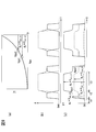
- FIG. 2A shows one cycle of the voltage applied to the LED drive circuit 80
- FIG. 2B shows the magnitude of the current I that flows when the voltage shown in FIG. 2A is applied. It is.
- the current I does not flow. This period is indicated by t1 in FIG.
- the first A current I flows from the one-part LED array 83 via the bypass circuit 801.
- the FET 85 operates at a constant current by feedback from the resistor 87 (hereinafter referred to as a first constant current operation state). This period is indicated by t2 in FIG.
- the LED drive circuit 80 includes a period in which the LEDs 83a and 84a are not lit at all, a period in which only the first partial LED row 83 is lit, and a first partial LED row 83 and a second partial LED row 84. Are both turned on.
- the luminous efficiency, power factor and total harmonics of the LED lighting device are controlled. It is known to improve distortion.
- FIG. 3 is an equivalent circuit block diagram of the conventional LED lighting device disclosed in Patent Document 2.
- the LED lighting device 900 has an LED drive circuit 90 and a commercial AC power source 92.
- the LED drive circuit 90 includes a bridge rectifier 91, a first partial LED string 93, a second partial LED string 94, a bypass circuit 901, a current limiting circuit 902, a first current detection resistor 903, and a second current detection. And a resistor 904.
- Each of the first partial LED array 93 and the second partial LED array 94 includes a plurality of LEDs connected in series.
- the bypass circuit 901, the current limiting circuit 902, the first current detection resistor 903, and the second current detection resistor 904 function as an LED current control circuit that controls the current flowing through the LED array.
- the bridge rectifier 91, the commercial AC power source 92, the first partial LED row 93, and the second partial LED row 94 correspond to the bridge rectifier 81, the commercial AC power source 82, the first partial LED row 83, and the second partial LED row 84, respectively. It has a configuration.
- the bypass circuit 901 includes an FET 95 that is an enhanced FET, and a bypass circuit current control unit 970.
- the bypass circuit current control unit 970 includes a bypass circuit reference power supply 971 and a bypass circuit variable power supply 972.
- the negative terminal of the bypass circuit reference power supply 971 is connected to the source of the FET 95
- the plus terminal of the bypass circuit reference power supply 971 is connected to the plus terminal of the bypass circuit variable power supply 972
- the minus terminal of the bypass circuit variable power supply 972 is connected to the gate of the FET 95.
- the gate-source voltage of the FET 95 is obtained by subtracting a voltage that is a constant multiple of the source voltage of the FET 95 (gain of the bypass circuit variable power source 972) from the voltage between both ends of the bypass circuit reference power source 971.
- the bypass circuit variable power source 972 when the current flowing through the first current detection resistor 903, that is, the drain current of the FET 95 increases, the voltage output to the gate of the FET 95 decreases. If the drain current of the FET 95 increases, the source voltage of the FET 95 (multiplied by a constant as described above) subtracted from the voltage of the bypass circuit reference power supply 971 increases, so the gate-source voltage of the FET 95 decreases and the drain current Try to reduce. Also, if the drain current of the FET 95 decreases, the source voltage of the FET 95 (multiplied by a constant as described above) subtracted from the voltage of the bypass circuit reference power supply 971 decreases, so that the gate-source voltage of the FET 95 rises and drains.
- the bypass circuit 901 is negatively fed by the first current detection resistor 903 and the second current detection resistor 904. At this time, by setting the resistance values of the first current detection resistor 903 and the second current detection resistor 904 to appropriate values, the bypass circuit 901 can perform a constant current operation with a desired current.
- the current limiting circuit 902 includes an FET 96 that is an enhanced FET and a constant current circuit current control unit 980.
- the constant current circuit current control unit 980 includes a current limit circuit reference power source 981 and a current limit circuit variable power source 982.
- the negative terminal of the current limit circuit reference power supply 981 is connected to the source of the FET 96, the plus terminal of the current limit circuit reference power supply 981 is connected to the plus terminal of the current limit circuit variable power supply 982, and the minus terminal of the current limit circuit variable power supply 982 is Connected to the gate of FET 96.
- the voltage between the gate and source of the FET 96 is obtained by subtracting a voltage that is a constant multiple of the source voltage of the FET 96 (gain of the current limit circuit variable power source 982) from the voltage between both ends of the current limit circuit reference power source 981.
- the current limiting circuit 902 has a configuration similar to that of the bypass circuit 901.
- the voltage output to the gate of the FET 96 decreases. If the drain current of the FET 96 increases, the source voltage of the FET 96 subtracted from the voltage of the current limit circuit reference power supply 981 (multiplied by a constant as described above) increases, so the gate-source voltage of the FET 96 decreases and the drain Try to reduce the current. If the drain current of the FET 96 decreases, the source voltage of the FET 96 subtracted from the voltage of the current limiting circuit reference power supply 981 (multiplied by a constant as described above) decreases, so that the gate-source voltage of the FET 96 increases.
- the current limiting circuit 902 is negatively fed by the second current detection resistor 904. At this time, by setting the resistance value of the second current detection resistor 904 to an appropriate value, the current limiting circuit 902 can perform a constant current operation with a desired current.
- the LED lighting device 900 has various problems caused by the first current detection resistor 903 and the second current detection resistor 904 being arranged to detect the current flowing through the bypass circuit 901 and the current limiting circuit 902, respectively. is there.
- the number of bypass circuits 901 is increased in order to improve the light emission efficiency and the like, the number of current detection resistors increases with an increase in the number of bypass circuits 901.
- the number of terminals increases according to the number of current detection resistors. Will do. Further, as the number of current detection resistors increases, the power consumption consumed by the current detection resistors increases.
- a second current detection resistor 904 that detects a current flowing in the current limiting circuit 902 located in the subsequent stage includes a first current detection resistor 903 that detects a current flowing in the bypass circuit 901 located in the preceding stage. Arranged between ground.
- the second current detection resistor 904 since the second current detection resistor 904 is disposed between the first current detection resistor 903 and the ground, the bypass circuit 901, the current limiting circuit 902, the first current detection resistor 903, and the second current detection resistor The connection relationship 904 is complicated.
- a current flows through the first current detection resistor 903 via the bypass circuit 901 in order to define the voltage of the bypass circuit variable power source 972 while the current flows through the second partial LED array. ing.
- This current contributes to an increase in the amount of light emitted from the first partial LED array 93.
- the voltage drop in the FET 95 is large, the power loss is large and the light emission efficiency of the LED lighting device 900 is reduced.
- An object of the present invention is to provide an LED current control circuit in which a bypass circuit and a constant current circuit are controlled based on a current detected by a single current detection resistor.
- the LED current control circuit includes a first partial LED string including a plurality of LEDs connected in series, and an LED including a plurality of LEDs connected in series and a second partial LED string connected in series with the first partial LED string.
- An LED current control circuit for controlling a current flowing in an LED string when a pulsating voltage is applied to the string, A current that includes a current limiting circuit input terminal and a current limiting circuit output terminal connected to the cathode of the last stage LED of the second partial LED row, and that limits the LED current flowing between the current limiting circuit input terminal and the current limiting circuit output terminal A limiting circuit;
- a bypass circuit input terminal connected between the first partial LED string and the second partial LED string, and a bypass circuit output terminal connected to the current limiting circuit output terminal;
- a bypass circuit that limits the bypass current that flows;
- a current detection element connected to the current limit circuit output terminal and the bypass circuit output terminal;
- the current limiting circuit limits the LED current based on current information detected by the current detection element and a predetermined first
- the current limiting circuit includes a first current limiting element that limits the magnitude of the LED current, and a first current control unit that controls the first current limiting element using the current information and the first coefficient.
- the bypass circuit includes a second current limiting element that limits the bypass current, and a second current control unit that controls the second current limiting element using the current information and the second coefficient. preferable.
- each of the first current limiting element and the second current limiting element is an FET
- the first current control unit includes a first reference power supply, a first variable power supply whose voltage is determined using current information and the first coefficient
- the second current control unit includes a second reference power source, a second variable power source whose voltage is determined using current information and the second coefficient
- the gate-source voltage of the first current limiting element is obtained by subtracting the voltage of the first variable power supply from the voltage of the first reference power supply
- the gate-source voltage of the second current limiting element is the voltage of the second reference power supply. It is preferable that the voltage of the second variable power supply is subtracted from.
- the first coefficient and the second coefficient, and the voltages of the first reference power supply and the second reference power supply are each variable.
- each of the first current limiting element and the second current limiting element is an FET
- the first current control unit includes a control FET of the first current control element, a first variable power supply whose voltage is determined using current information and the first coefficient
- the second current control unit includes a control FET of the second current control element, a second variable power source whose voltage is determined using current information and the second coefficient
- the gate-source voltage of the control FET of the first current control element is determined based on the voltage of the first variable power supply
- the gate-source voltage of the control FET of the second current control element is the voltage of the second variable power supply. Is preferably determined based on
- the first coefficient and the second coefficient are preferably variable.
- the LED current control circuit further includes a third reference power supply, and the control FET of the first current control element and the control FET of the second current control element operate based on the voltage from the third reference power supply. Is preferred.
- the LED current control circuit further includes a fourth reference power supply, and the voltages of the first variable power supply and the second variable power supply are varied in conjunction with the voltage of the fourth reference power supply.
- each of the first current limiting element and the second current limiting element is an FET
- the first current control unit includes a control operational amplifier for the first current control element
- the second current control unit includes a control operational amplifier for the second current control element
- the voltage corresponding to the current information and the voltage of the first reference power supply are input to the differential input terminal of the control operational amplifier of the first current control element, and the current is input to the differential input terminal of the control operational amplifier of the second current control element.
- the voltage corresponding to the information and the voltage of the second reference power supply are input,
- the gate-source voltage of the first current limiting element is determined based on the output of the control operational amplifier of the first current control element, and the gate-source voltage of the second current limiting element is determined as the control operational amplifier of the second current control element. Preferably, it is determined based on the output of.
- the first coefficient and the second coefficient, and the voltages of the first reference power supply and the second reference power supply are preferably variable.
- each of the first current limiting element and the second current limiting element is an FET
- the first current control unit includes a control operational amplifier for the first current control element
- the second current control unit includes a control operational amplifier for the second current control element
- the voltage corresponding to the current information and the voltage of the first variable power supply are input to the differential input terminal of the control operational amplifier of the first current control element, and the current is input to the differential input terminal of the control operational amplifier of the second current control element.
- the voltage corresponding to the information and the voltage of the second variable power supply are input,
- the gate-source voltage of the first current limiting element is determined based on the output of the control operational amplifier of the first current control element, and the gate-source voltage of the second current limiting element is determined as the control operational amplifier of the second current control element. Preferably, it is determined based on the output of.
- the LED current control circuit further includes a fourth reference power supply, and the voltages of the first variable power supply and the second variable power supply are varied in conjunction with the voltage of the fourth reference power supply.
- the LED current control circuit further includes a third reference power supply, and the control operational amplifier of the first current control element and the control operational amplifier of the second current control element operate based on the voltage from the third reference power supply. Is preferred.
- the LED string further includes a third partial LED string including a plurality of LEDs connected in series and connected in series between the first partial LED string and the second partial LED string, and a bypass circuit.
- the input terminal is connected between the first partial LED row and the third partial LED row,
- a second bypass circuit having a second bypass circuit input terminal connected between the second partial LED string and the third partial LED string; and a second bypass circuit output terminal connected to the current limiting circuit output terminal.
- a second bypass circuit for limiting a second bypass current flowing between the terminal input terminal and the second bypass circuit terminal output terminal;
- the second bypass circuit restricts the second bypass current based on the current information detected by the current detection element and a predetermined third coefficient according to the state of the pulsating voltage, and the third partial LED array It is preferable to control so that the current that has flowed from the current to the current detection element via the second bypass circuit flows toward the second partial LED array without passing through the second bypass circuit.
- the LED current control circuit includes a first partial LED string including a plurality of LEDs connected in series, and a second partial LED string including a plurality of LEDs connected in series and connected in series with the first partial LED string.
- a current control circuit for controlling a current flowing through the LED array when a pulsating voltage is applied to the LED array including the current limiting circuit input terminal connected to the cathode of the LED in the final stage of the second partial LED array And a current limiting circuit output terminal, and is connected between the first partial LED string and the second partial LED string, and a current limiting circuit that limits the LED current flowing between the current limiting circuit input terminal and the current limiting circuit output terminal.
- a current limit circuit output terminal and a current detection element connected to the bypass circuit output terminal.
- the current limit circuit includes current information detected by the current detection element and a predetermined first coefficient. The LED current is limited based on the current value detected by the current detection element and a second coefficient different from the predetermined first coefficient according to the state of the pulsating voltage. The current is limited, and the current flowing from the first partial LED string to the current detection element via the bypass circuit is controlled to flow toward the second partial LED string without passing through the bypass circuit.
- an LED current control circuit in which a bypass circuit and a constant current circuit are controlled based on a current detected by a single current detection resistor.
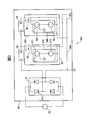
- FIG. 3 is a circuit block diagram of the LED lighting device 100.
- FIG. 3 is a circuit block diagram of an internal circuit of a bypass circuit current control unit 170.
- FIG. 3 is a circuit block diagram of an internal circuit of a current limiting circuit current control unit 180.
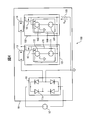
- FIG. 6 is a circuit block diagram of another LED lighting device 200.
- A) is a figure which shows the voltage-current characteristic of FET which LED lighting apparatus 200 has
- (b) is a figure which shows drain current of FET which LED lighting apparatus 100 has
- (c) is LED lighting apparatus 100 It is a figure which shows the gate-source voltage of FET which has.
- FIG. 6 is a circuit block diagram of another LED lighting device 200.
- (A) is a figure which shows the voltage-current characteristic of FET which LED lighting apparatus 200 has
- (b) is a figure which shows drain current of FET which LED lighting apparatus 200 has
- (c) is LED lighting apparatus 200 It is a figure which shows the gate-source voltage of FET which has.
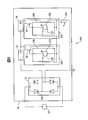
- FIG. 6 is a circuit block diagram of still another LED lighting device 110.
- (A) is a figure which shows the voltage-current characteristic of FET which LED lighting apparatus 110 has
- (b) is a figure which shows drain current of FET which LED lighting apparatus 110 has
- (c) is a figure which shows LED lighting apparatus 110 It is a figure which shows the gate-source voltage of FET which has.
- (A) is a figure which shows the relationship between the voltage-current characteristic of FET which the LED lighting apparatus 110 has, and the voltage-current characteristic of a current control part
- (b) is the elements on larger scale of (a).
- (A) is a figure which shows the voltage-current characteristic of FET when the leakage current has arisen in LED lighting apparatus 110
- (b) is a figure which shows the drain current of FET in the case of (a)
- (c) is a figure which shows the gate-source voltage of FET in the case of (a).
- (A) is a figure which shows the relationship between the voltage-current characteristic of FET in the case of FIG. 13, and the voltage-current characteristic of a current control part
- (b) is the elements on larger scale of (a).
- FIG. 6 is a circuit block diagram of still another LED lighting device 210.
- (A) is a figure which shows the voltage-current characteristic of FET which the LED lighting apparatus 210 has
- (b) is a figure which shows the drain current of FET which the LED lighting apparatus 210 has
- (c) is a figure which shows LED lighting apparatus 210. It is a figure which shows the gate-source voltage of FET which has.
- (A) is a figure which shows the relationship between the voltage-current characteristic of FET which the LED lighting apparatus 210 has, and the voltage-current characteristic of a current control part
- (b) is the elements on larger scale of (a).
- (A) is a circuit block diagram of yet another LED lighting device 300
- (b) is a circuit block diagram of yet another LED lighting device 310
- (c) is a circuit block diagram of yet another LED lighting device 320.
- FIG. (A) is a figure which shows the drain current of FET of LED lighting apparatus 300 shown to Fig.20 (a)
- (b) is a figure which shows the drain current of FET of LED lighting apparatus 310 shown in FIG.20 (b).
- FIG. 21C is a diagram showing the drain current of the FET of the LED lighting device 320 shown in FIG. (A) is a circuit block diagram of yet another LED lighting device 330
- (b) is a circuit block diagram of yet another LED lighting device 340.
- (A) is a figure which shows the drain current of FET of LED lighting apparatus 330 shown to Fig.22 (a)
- (b) is a figure which shows the drain current of FET of LED lighting apparatus 340 shown in FIG.22 (b). is there.
- FIG. 6 is a circuit block diagram of still another LED lighting device 400. It is a figure which shows the electric current Isen which flows through the electric current detection resistance 410 of the LED lighting apparatus 400 shown in FIG.
- FIG. 10 is a circuit block diagram of still another LED lighting device 420.
- FIG. 10 is a circuit block diagram of still another LED lighting device 440.
- FIG. 6 is a circuit block diagram of still another LED lighting device 500. It is a circuit block diagram of another LED lighting device 510.
- FIG. 4 is a circuit block diagram of the LED lighting device 100.
- the LED lighting device 100 includes an LED drive circuit 10 and a commercial AC power supply 12.
- the LED drive circuit 10 includes a bridge rectifier 11, a first partial LED string 13, a second partial LED string 14, a bypass circuit 101, a current limiting circuit 102, and a current detection resistor 103.
- Each of the first partial LED row 13 and the second partial LED row 14 has a plurality of LEDs connected in series.
- the bypass circuit 101, the current limiting circuit 102, and the current detection resistor 103 function as an LED current control circuit that controls the current flowing through the LED string.
- the bridge rectifier 11, the commercial AC power source 12, the first partial LED row 13 and the second partial LED row 14 correspond to the bridge rectifier 81, the commercial AC power source 82, the first partial LED row 83 and the second partial LED row 84, respectively. It has the composition to do.
- the bypass circuit 101 includes an FET 15 that is an enhancement type FET and a bypass circuit current control unit 170.
- the drain of the FET 15 is a bypass current input terminal connected between the first partial LED string 13 and the second partial LED string 14.
- the source of the FET 15 is a bypass current output terminal connected to one terminal of the current detection resistor 103.
- the current limiting circuit 102 includes an FET 16 that is an enhanced FET and a current limiting circuit current control unit 180.
- the drain of the FET 16 is a limiting current input terminal connected to the cathode of the LED in the final stage of the second partial LED row 14.
- the source of the FET 16 is a limited current output terminal connected to one terminal of the current detection resistor 103.
- FIG. 5 is a circuit block diagram of an internal circuit of the bypass circuit current control unit 170.
- the bypass circuit current control unit 170 includes a bypass circuit reference power supply 171 and a bypass circuit variable power supply 172.
- Bypass circuit reference power 171 includes an operational amplifier 1710, and the 11 resistance 1711 resistance value of R 11, the resistance value of the 12th resistor 1712 is R 12.
- the twelfth resistor 1712 is a variable resistor. A voltage of 1 V is input to the positive input terminal of the operational amplifier 1710.
- V ref (1+ (R 12 / R 11 )) ⁇ 1V Is output.
- the bypass circuit variable power source 172 includes an amplifying unit 173, a first subtracting unit 174, and a second subtracting unit 175.
- Amplifying unit 173 includes an operational amplifier 1730, and the 31 resistance 1731 resistance value is R 31, the resistance value of the first 72 resistor 1732 is R 72.
- the 72nd resistor 1732 is a variable resistor.
- the inter-terminal voltage V sen of the current detection resistor 103 is input to the positive input terminal of the operational amplifier 1730.
- V sen1 (1+ (R 72 / R 31 )) ⁇ V sen Is output.
- V sen1 g b ⁇ V sen It becomes.
- V 40out (1+ (R 44 / R 43 )) ⁇ ((R 42 / (R 41 + R 42 )) V sen1 ⁇ (R 44 / (R 43 + R 44 )) V sen ) Is output.
- V 40out V sen1 -V sen It can be.
- the second subtracting unit 175, an operational amplifier 1750, and the 51 resistance 1751 resistance value is R 51
- the 52 resistance 1752 resistance value is R 52
- the 53 resistance 1753 resistance value is R 53
- resistance and a 54th resistor 1754 is R 54.
- V 50out (1+ (R 54 / R 53 )) ⁇ [(R 52 / (R 51 + R 52 )) V ref ⁇ (R 54 / (R 53 + R 54 )) V 40out ] Is output.
- the negative terminal of the bypass circuit reference power supply 171 shown in FIG. 4 was connected to one end of the current detection resistor, and the voltage was Vsen .
- the voltage between the plus terminal and the minus terminal is V ref
- the voltage at the plus terminal is (V ref + V sen ).
- g b ⁇ V sen is output.
- V sen is not input to the bypass circuit reference power source 171 shown in FIG. 5, and the output of the operational amplifier 1810 is V ref .
- V 50out V ref ⁇ g b ⁇ V sen + V sen ) matches the output of the bypass variable power supply 172 shown in FIG.
- bypass circuit reference power source 171 shown in FIG. 4 and the bypass circuit reference power source 171 shown in FIG. 5 do not completely match.
- a part of the function of the bypass circuit reference power source 171 shown in FIG. 4 (the voltage V ref is shifted by the voltage V sen ) is included in the bypass circuit variable power source 172 shown in FIG.
- the bypass circuit variable power supply 172 of FIG. 5 one end of the 43rd resistor R43 to which the voltage V sen is input corresponds to the negative terminal of the bypass circuit reference power supply 171 shown in FIG.
- FIG. 6 is a circuit block diagram of an internal circuit of the current limiting circuit current control unit 180.
- the current limit circuit current control unit 180 includes a current limit circuit reference power source 181 and a current limit circuit variable power source 182.
- the current limiting circuit reference power source 181 has the same configuration as the bypass circuit reference power source 171. As in FIG. 5, the current limiting circuit current control unit 180 shown in FIG. 6 and the current limiting circuit current control unit 180 shown in FIG. 4 do not completely match, but FIG. 4 and FIG. 6 and the gate voltage Vg applied to the FET 16 is equal.
- V ref (1+ (R 12 / R 11 )) ⁇ 1V Is output.
- the current limiting circuit variable power source 182 includes an amplifying unit 183, a first subtracting unit 184, and a second subtracting unit 185.
- the first subtraction unit 184 has the same configuration as the first subtraction unit 174 of the bypass circuit variable power supply 172
- the second subtraction unit 185 has the same configuration as the second subtraction unit 175 of the bypass circuit variable power supply 172. .
- Amplifying unit 183 includes an operational amplifier 1830, and the 31 resistance 1831 resistance value is R 31, the resistance value of the first 82 resistor 1832 is R 82.
- the 82nd resistor 1832 is a variable resistor.
- the inter-terminal voltage V sen of the current detection resistor 103 is input to the positive input terminal of the operational amplifier 1830.
- V sen2 (1+ (R 82 / R 31 )) ⁇ V sen Is output.
- V sen2 g c ⁇ V sen It becomes.
- V 40out (1+ (R 44 / R 43 )) ⁇ ((R 42 / (R 41 + R 42)) V sen2 - (R 44 / (R 43 + R 44)) V sen) Is output.
- V 50out (1+ (R 54 / R 53 )) ⁇ [(R 52 / (R 51 + R 52 )) V ref ⁇ (R 54 / (R 53 + R 54 )) V 40out ] Is output.
- the amplifying unit 173 of the bypass circuit variable power source 172 and the amplifying unit 183 of the current limiting circuit variable power source 182 have different gains by making the resistance value of the 72nd resistor 1732 and the resistance value of the 82nd resistor 1832 different. I am letting.
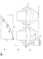
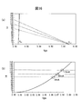
- FIG. 7 is a diagram showing various characteristics of the LED lighting device 100.
- FIG. 7A is a diagram showing the relationship between the Vgs-Id curves of the FETs 15 and 16 and the voltages generated by the amplification units 173 and 183.
- the horizontal axis indicates the gate-source voltage Vgs of the FETs 15 and 16
- the vertical axis indicates the drain current Id of the FETs 15 and 16.
- FIG. 7B is a diagram showing a change with time of the drain current Id of the FET 15, the drain current Id of the FET 16, and the total value of the drain currents Id of the FETs 15 and 16.
- the horizontal axis represents the time for one cycle of the full-wave rectified waveform
- the vertical axis represents the drain current Id of the FETs 15 and 16.
- the solid line indicates the drain current Id of the FET 15
- the broken line indicates the drain current Id of the FET 16
- the alternate long and short dash line indicates the total current of the drain currents of the FETs 15 and 16.
- FIG. 7 (c) is a diagram showing changes over time in the gate-source voltage Vgs of the FET 15 and the gate-source voltage Vgs of the FET 16.
- the horizontal axis indicates the time corresponding to the horizontal axis in FIG. 7B
- the vertical axis indicates the gate-source voltage Vgs of the FETs 15 and 16.
- the solid line indicates the gate-source voltage Vgs of the FET 15
- the broken line indicates the gate-source voltage Vgs of the FET 16.
- the applied voltage is equal to or lower than the threshold voltage of the first partial LED array 13, and no current flows through both the first partial LED array 13 and the second partial LED array 14. It is a period.
- the applied voltage is larger than the threshold voltage of the first partial LED row 13 and the threshold voltage of the first partial LED row 13 and the threshold voltage of the second partial LED row 14
- the period is equal to or lower than the total voltage and the current is flowing through the first partial LED array 13.
- the applied voltage becomes larger than the total voltage of the threshold voltage of the first partial LED string 13 and the threshold voltage of the second partial LED string 14, and the first partial LED string. 13 is a period in which current flows in both the second partial LED row 14.
- a current flows through both the first partial LED array 13 and the second partial LED array 14.
- the potential difference generated in the current detection resistor 103 in the period t3 is V sen_t3
- the gate-source voltage Vgs of the FET 15 is V ref ⁇ g b ⁇ V sen_t3
- the gate-source voltage Vgs of the FET 16 is V ref ⁇ g c ⁇ V sen_t3. It becomes.
- V ref ⁇ g c ⁇ V sen — t3 which is the gate-source voltage Vgs of the FET 16, is equal to Vgs 2 in FIGS. 7A and 7C.
- V ref ⁇ g b ⁇ V sen — t3 which is the gate-source voltage Vgs of the FET 15, is smaller than the threshold voltage of the FET 15, no current flows through the bypass circuit 101 during the period t 3.
- the bypass circuit 101 controls the current flowing through the current detection resistor 103 through the bypass circuit 101 in the period t2 to flow toward the second partial LED array 14 in the period t3.
- the bypass circuit current control unit 170 and the current limiting circuit current control unit 180 are controlled based on the current detected by the single current detection resistor 103. .
- FIG. 8 is a circuit block diagram of another LED lighting device 200.
- the LED lighting device 200 includes an LED drive circuit 20 and a commercial AC power supply 22.
- the LED drive circuit 20 includes a bridge rectifier 21, a first partial LED string 23, a second partial LED string 24, a bypass circuit 201, a current limiting circuit 202, and a current detection resistor 203.
- Each of the first partial LED array 23 and the second partial LED array 24 has a plurality of LEDs connected in series.
- the bypass circuit 201, the current limiting circuit 202, and the current detection resistor 203 function as an LED current control circuit that controls the current flowing through the LED string.
- the bridge rectifier 21, the commercial AC power source 22, the first partial LED row 23, and the second partial LED row 24 correspond to the bridge rectifier 81, the commercial AC power source 82, the first partial LED row 83, and the second partial LED row 84, respectively. It has the composition to do.
- the bypass circuit 201 includes an FET 25 that is a depletion type FET and a bypass circuit current control unit 270.
- the current limiting circuit 202 includes a FET 26 that is a depletion type FET, and a current limiting circuit current control unit 280.
- the bypass circuit current control unit 270 is different from the bypass circuit current control unit 170 in that it has only a bypass circuit variable power source 272 corresponding to the bypass circuit variable power source 172 without having a configuration corresponding to the bypass circuit reference power source 171. .
- the current limit circuit current control unit 280 does not have a configuration corresponding to the current limit circuit reference power source 181, but includes only the current limit circuit variable power source 282 corresponding to the current limit circuit variable power source 182. This is different from the current control unit 180. Since the threshold voltages of the FET 25 and the FET 26 arranged in the bypass circuit current control unit 270 and the current limiting circuit current control unit 280 are sufficiently smaller than 0 V, the gate voltage does not need to be raised, so the reference power supply is arranged Not.
- FIG. 9 is a diagram illustrating various characteristics of the LED lighting device 200.
- FIG. 9A shows the relationship between the Vgs-Id curves of the FETs 25 and 26 and the voltages generated by the bypass circuit current control unit 270 and the current limiting circuit current control unit 180.
- the horizontal axis represents the gate-source voltage Vgs of the FETs 25 and 26, and the vertical axis represents the drain current Id of the FETs 25 and 26.
- FIG. 9B is a diagram showing the change over time of the drain current Id of the FET 25, the drain current Id of the FET 26, and the total value of the drain currents Id of the FETs 25 and 26.
- the horizontal axis represents the time for one cycle of the full-wave rectified waveform
- the vertical axis represents the drain current Id of the FETs 25 and 26.
- the solid line indicates the drain current Id of the FET 25
- the broken line indicates the drain current Id of the FET 26
- the alternate long and short dash line indicates the total current of the drain currents of the FETs 25 and 26.
- FIG. 9C is a diagram showing temporal changes in the absolute values of the gate-source voltage Vgs of the FET 25, the gate-source voltage Vgs of the FET 26, and the terminal voltage of the current detection resistor 203.
- the horizontal axis indicates the time corresponding to the horizontal axis in FIG. 7B
- the vertical axis indicates the gate-source voltage Vgs (absolute value) of the FETs 25 and 26.
- the solid line indicates the absolute value of the gate-source voltage Vgs of the FET 25, the broken line indicates the absolute value of the gate-source voltage Vgs of the FET 26, and the alternate long and short dash line indicates the voltage between the terminals of the current detection resistor 203. .
- the applied voltage is equal to or lower than the threshold voltage of the first partial LED array 23, and no current flows through both the first partial LED array 23 and the second partial LED array 24. It is a period.
- the applied voltage is larger than the threshold voltage of the first partial LED row 23, and the threshold voltage of the first partial LED row 23 and the threshold voltage of the second partial LED row 24 The period is equal to or lower than the total voltage and the current is flowing through the first partial LED array 23.
- the applied voltage becomes larger than the total voltage of the threshold voltage of the first partial LED array 23 and the threshold voltage of the second partial LED array 24 during the period shown. This is a period during which current flows through both the first partial LED row 23 and the second partial LED row 24.
- a current flows through both the first partial LED row 23 and the second partial LED row 24.
- the potential difference generated in the current detection resistor 203 in the period t3 is V sen_t3
- the gate-source voltage Vgs of the FET 25 is ⁇ g b ⁇ V sen_t3
- the gate-source voltage Vgs of the FET 26 is ⁇ g c ⁇ V sen_t3 .
- ⁇ g c ⁇ V sen — t3 which is the gate-source voltage Vgs of the FET 26 is equal to Vgs2 in FIGS. 9A and 9C (shown as an absolute value in FIG. 9).
- bypass circuit 201 controls the current flowing through the current detection resistor 203 through the bypass circuit 201 in the period t2 to flow toward the second partial LED array 14 in the period t3.
- the LED lighting device 200 is configured such that the bypass circuit current control unit 270 and the current limiting circuit current control unit 280 are controlled based on the current detected by the single current detection resistor 203. .
- the bypass circuit 201 based on the second coefficient that is different from the current information and a first coefficient detected by the current detecting element (current limiting circuit gain g b), has been flowing in the first portion LED string 23 current Is controlled to flow toward the second partial LED row 24 without going through the bypass circuit.
- FIG. 10 is a circuit block diagram of still another LED lighting device 110.
- the LED lighting device 110 includes an LED drive circuit 111 and a commercial AC power supply 12.
- the LED drive circuit 111 is different from the LED drive circuit 10 in that it includes a first bypass circuit 101a and a second bypass circuit 101b having a configuration corresponding to the bypass circuit 101.
- the LED lighting device 110 is different from the LED 100 in that the LED row is divided into a first partial LED row 13a, a second partial LED row 13b, and a third partial LED row 14.
- the first bypass circuit 101a includes an FET 15a, which is an enhanced FET, and a first bypass circuit current control unit 170a.
- the first bypass circuit current control unit 170a includes a first bypass circuit reference power source 171a and a first bypass circuit variable power source 172a.
- the gain of the first bypass circuit variable power source 172a is g b1 .
- the first bypass circuit 101a controls the current flowing through the current detection resistor 103 via the first bypass circuit 101a to flow toward the second partial LED row 13b according to the state of the pulsating voltage.
- the second bypass circuit 101b includes an FET 15b, which is an enhanced FET, and a second bypass circuit current control unit 170b.
- the second bypass circuit current control unit 170b includes a second bypass circuit reference power source 171b and a second bypass circuit variable power source 172b.
- Gain of the second bypass circuit variable power source 172b is g b2.
- the second bypass circuit 101b controls the current flowing through the current detection resistor 103 via the second bypass circuit 101b to flow toward the third partial LED array 14 according to the state of the pulsating voltage.
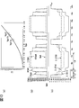
- FIG. 11 and 12 are diagrams illustrating various characteristics of the LED lighting device 110.
- FIG. 11 and 12 are diagrams illustrating various characteristics of the LED lighting device 110.
- FIG. 11A shows the relationship between the Vgs-Id curves of the FETs 15a, 15b and 16 and the voltages generated by the first and second bypass circuit current control units 170a and 170b and the current limiting circuit current control unit 180.
- FIG. The vertical axis and horizontal axis in FIG. 11A correspond to the vertical axis and horizontal axis in FIG. 7A, respectively.
- FIG. 11B is a diagram showing a change with time of the drain current Id of the FET 15a, the drain current Id of the FET 15b, the drain current Id of the FET 16, and the total values of the drain currents Id of the FETs 15a, 15b and 16.
- the vertical axis and horizontal axis in FIG. 11B correspond to the vertical axis and horizontal axis in FIG. 7B, respectively.
- the solid line indicates the drain current Id of the FET 15a
- the broken line indicates the drain current Id of the FET 15b
- the alternate long and short dash line indicates the drain current Id of the FET 16.
- the two-dot chain line indicates the total current of the drain currents of the FETs 15a, 15b and 16.
- FIG. 11 (c) is a diagram showing a change with time of the gate-source voltage Vgs of the FETs 15a, 15b, and 16.
- FIG. The vertical axis and the horizontal axis in FIG. 11C correspond to the vertical axis and the horizontal axis in FIG.
- the solid line indicates the gate-source voltage Vgs of the FET 15a
- the broken line indicates the gate-source voltage Vgs of the FET 15b
- the alternate long and short dash line indicates the gate-source voltage Vgs of the FET 16.
- the period t1 shown in FIG. 11C is a period in which no current flows through all of the first partial LED row 13a, the second partial LED row 13b, and the third partial LED row 14.
- a period t2 shown in FIG. 11C is a period in which a current flows only in the first partial LED row 13a.
- a period t3 illustrated in FIG. 11C is a period in which a current flows through the first partial LED array 13a and the second partial LED array 13b.
- the period indicated by t4 is a period in which current flows through all of the first partial LED row 13a, the second partial LED row 13b, and the third partial LED row 14.
- the gate-source voltage Vgs of FET15a is V ref -g b1 ⁇ V sen_t2 next, the gate-source voltage Vgs of FET15b is V ref -g b2 ⁇ V sen_t2 It becomes.
- the gate-source voltage Vgs of the FET 16 is V ref ⁇ g c ⁇ V sen — t 2 .
- V ref ⁇ g b1 ⁇ V sen — t2 which is the gate-source voltage Vgs of the FET 15a is equal to Vgs1a in FIGS. 11 (a) and 11 (c).
- a current flows through the first partial LED row 13a and the second partial LED row 13b.
- the gate-source voltage Vgs of the FET 15a is V ref ⁇ g b1 ⁇ V sen_t3
- the gate-source voltage Vgs of the FET 15b is V ref ⁇ g b2 ⁇ V sen_t3. It becomes.
- the gate-source voltage Vgs of the FET 16 is V ref ⁇ g c ⁇ V sen — t3 .
- V ref ⁇ g b2 ⁇ V sen — t2 that is the gate-source voltage Vgs of the FET 15b is equal to Vgs1b in FIGS. 11 (a) and 11 (c).
- a current flows through all of the first partial LED row 13a, the second partial LED row 13b, and the third partial LED row 14.
- the gate-source voltage Vgs of the FET 15a is V ref ⁇ g b1 ⁇ V sen_t4
- the gate-source voltage Vgs of the FET 15b is V ref ⁇ g b2 ⁇ V sen_t4. It becomes.
- the gate-source voltage Vgs of the FET 16 is V ref ⁇ g c ⁇ V sen_t4 .
- V ref ⁇ g c ⁇ V sen — t4 which is the gate-source voltage Vgs of the FET 16 is equal to Vgs2 in FIGS. 11A and 11C.
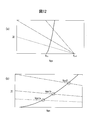
- FIG.12 (b) is the elements on larger scale of the figure shown to Fig.12 (a).
- the horizontal axis indicates the gate-source voltage Vgs of the FETs 15a, 15b, and 16, and the vertical axis indicates the drain current of the FETs 15a, 15b, and 16. In each of FIGS.
- the solid lines indicate the voltage-current characteristics of the FETs 15a, 15b, and 16
- the broken lines indicate the relationship between the output voltage of the first bypass circuit current control unit 170a and the current flowing through the current detection resistor.
- the alternate long and short dash line indicates the relationship between the output voltage of the second bypass circuit current control unit 170b and the current flowing through the current detection resistor.
- the alternate long and two short dashes line indicates the output voltage of the current limiting circuit current control unit 180 and the current flowing through the current detection resistor. Show the relationship.
- Each output voltage corresponds to the gate-source voltage Vgs of the FETs 15a, 15b, and 16 when the first bypass circuit 101a, the second bypass circuit 101b, or the current limiting circuit 102 is operating independently.
- the current flowing through the current detection resistor corresponds to the drain current Id of the FETs 15a, 15b, and 16 when the first bypass circuit 101a, the second bypass circuit 101b, or the current limiting circuit 102 is operating independently.
- R s is the resistance value of the current detection resistor 103.
- Vgs V ref ⁇ g b1 ⁇ R s ⁇ Id It becomes the relationship. This corresponds to the broken line in FIG.
- the drain current Id and the gate-source voltage Vgs have a non-linear relationship.
- Id f (Vgs) It can be expressed as.
- f represents a function and corresponds to a curve indicated by a solid line in FIG.
- the operating point is obtained by combining the above two equations, and in FIG. 12 (a), it is the intersection of a broken line and a curve.
- the drain current Id flows only in the FET 15a, and the feedback from the current detection resistor 103 is effective only in the first bypass circuit 101a. Therefore, the first bypass circuit 101a is in the current detection resistor. 103 is equivalent to the state of operating independently.
- Vgs V ref ⁇ g b2 ⁇ R s ⁇ Ids It becomes the relationship. This corresponds to the alternate long and short dash line in FIG.
- the state in which the second bypass circuit 101b is operating alone together with the current detection resistor 103 is indicated by the intersection of the alternate long and short dash line and the curve, and the period t3 in which the drain current Id flows only through the FET 15b in FIG. (See FIG. 11C).
- Vgs V ref ⁇ g c ⁇ R s ⁇ Id
- the state where the current limiting circuit 102 is operating alone together with the current detection resistor 103 is indicated by the intersection of the two-dot chain line and the curve, and the period t4 during which the drain current Id flows only through the FET 16 in FIG. (See FIG. 11C).
- the first bypass circuit 101a, the second bypass circuit 101b, and the current limiting circuit 102 are independently operated together with the current detection resistor 103, the output voltage (Vgs) and current of each circuit (101a, 101b, 102) A straight line indicating the relationship with the current (Id) flowing through the detection resistor 103 and a curve indicating the gate-source voltage-current characteristics of the FETs (15a, 15b, 16) included in each circuit (101a, 101b, 102). The intersection is the operating point of the FET.
- the first bypass circuit 101a, the second bypass circuit 101b, and the current limiting circuit 102 operate independently during the periods t2, t3, and t4 shown in FIG.
- the first By determining the gains g b1 , g b2, and g c of the bypass circuit variable power source 172a, the second bypass circuit variable power source 172b, and the current limiting circuit variable power source 182, the first partial LED row 13a, the second LED 13b, and the third partial LED The current flowing through the column 14 can be determined.
- the first bypass circuit 101a is cut off when the second bypass circuit 101b is operating at a constant current.
- the current limiting circuit 102 operates at a constant current
- the first and second bypass circuits 101a and 101b are cut off.
- the voltage V ref and the gains g b1 , g b2 , and g c are set inappropriately, for example, a leakage current may be generated in the second bypass circuit 101b when the current limiting circuit 102 is operating at a constant current. is there.
- FIGS. 13 to 16 are diagrams for explaining the leakage current preventing function in the LED lighting device 110.
- FIGS. 13 and 14 are diagrams illustrating electrical characteristics when a leakage current is generated in the LED lighting device 110
- FIGS. 15 and 16 are diagrams illustrating electrical characteristics when no leakage current is generated in the LED lighting device 110. is there. 13 and 15 correspond to FIG. 11, and FIGS. 14 and 16 correspond to FIG.
- an AC voltage having an amplitude of 120V is applied to the commercial AC power supply 12
- the threshold voltages of the FETs 15a, 15b, and 16 are 3.8V
- the resistance value of the current detection resistor 103 is 1 ⁇ .
- the voltages of the first bypass circuit reference power source 171a, the second bypass circuit reference power source 171b, and the current limiting circuit reference power source 181 are 4.1V.
- the gain g b1 of the first bypass circuit variable power source 172a is 3.4
- the gain g b2 of the second bypass circuit variable power source 172b is 2.5
- the gain g c of the current limit circuit variable power source 182 is 2.0. It is.
- the voltages of the first bypass circuit reference power supply 171a, the second bypass circuit reference power supply 171b, and the current limiting circuit reference power supply 181 are 8.0V.
- the gain g b1 of the first bypass circuit variable power source 172a is 59.1
- the gain g b2 of the second bypass circuit variable power source 172b is 45.9
- the gain g c of the current limit circuit variable power source 182 is 37.5. It is.
- a current of 70 mA flows through the FET 15a, and no current flows through the FETs 15b and 16, so the total current becomes 70 mA.
- a current of 91 mA flows through the FET 15b and no current flows through the FETs 15a and 16, so the total current becomes 91 mA.
- a leakage current is generated in the bypass circuit 101b in the period t4 shown in FIG. At this time, although the total current is 112 mA, the current flowing through the FET 16 is 104 mA, and a current of 8 mA flows through the FET 15 b.
- a current of 70 mA flows through the FET 15a and no current flows through the FETs 15b and 16, so the total current becomes 70 mA.
- a current of 90 mA flows through the FET 15b and no current flows through the FETs 15a and 16, so the total current becomes 90 mA.
- a current of 110 mA flows through the FET 16, and no current flows through the FETs 15a and 15b, so the total current becomes 110 mA.
- Vgs V ref
- the control unit 180 is controlled.
- the LED lighting device 110 uses the first bypass circuit 101a and the second bypass circuit 101b based on the current information detected by the current detection element and predetermined coefficients (gains g b1 , g b2 , g c ). Thus, current switching control among the first partial LED row 13a, the second partial LED row 13b, and the third partial LED row 14 is performed.
- FIG. 17 is a circuit block diagram of still another LED lighting device 210.
- the LED lighting device 210 has an LED drive circuit 211 and a commercial AC power supply 22.
- the LED drive circuit 211 is different from the LED drive circuit 20 in that it includes a first bypass circuit 201a and a second bypass circuit 201b having a configuration corresponding to the bypass circuit 201.
- the LED lighting device 210 is different from the LED lighting device 200 in that the LED row is divided into a first partial LED row 23a, a second partial LED row 23b, and a third partial LED row 24.
- the first bypass circuit 201a includes an FET 25a that is a depletion type FET, and a first bypass circuit current control unit 270a.
- the first bypass circuit current control unit 270a includes a first bypass circuit variable power supply 272a gain is g b1.
- the second bypass circuit 201b includes an FET 25b that is a depletion type FET, and a second bypass circuit current control unit 270b.
- the second bypass circuit current control unit 270b includes a second bypass circuit variable power source 272b gain is g b2.
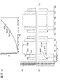
- FIG. 18 and 19 are diagrams showing various characteristics of the LED lighting device 210.
- FIG. 18 and 19 are diagrams showing various characteristics of the LED lighting device 210.
- FIG. 18A is a diagram showing the relationship between the Vgs-Id curves of the FETs 25a, 25b, and 26 and the voltages generated by the amplifying units 273a, 273b, and 283.
- FIG. 18B is a diagram showing temporal changes in the drain current Id of the FET 25a, the drain current Id of the FET 25b, the drain current Id of the FET 26, and the total values of the drain currents Id of the FETs 25a, 25b and 16.
- FIG. 18C is a diagram showing the change over time of the gate-source voltage Vgs (absolute value) of the FETs 25a, 25b and 26.
- 18A to 18C correspond to the vertical and horizontal axes of FIGS. 9A to 9C, respectively.
- the solid line indicates the drain current Id of the FET 25a
- the broken line indicates the drain current Id of the FET 25b
- the alternate long and short dash line indicates the drain current Id of the FET 26.
- the two-dot chain line indicates the total current of the drain currents of the FETs 25a, 25b and 26.
- the solid line indicates the gate-source voltage Vgs of the FET 25a
- the broken line indicates the gate-source voltage Vgs of the FET 25b
- the alternate long and short dash line indicates the gate-source voltage Vgs of the FET 26.
- a period t1 shown in FIG. 18C is a period in which no current flows in all of the first partial LED row 23a, the second partial LED row 23b, and the third partial LED row 24.
- a period t2 illustrated in FIG. 18C is a period in which a current flows only in the first partial LED row 23a.
- a period t3 illustrated in FIG. 18C is a period in which a current flows through the first partial LED array 23a and the second partial LED array 23b.
- a period t4 shown in FIG. 18C is a period in which a current flows through all of the first partial LED array 23a, the second partial LED array 23b, and the third partial LED array 24.
- a current flows only through the first partial LED row 23a.
- the gate-source voltage Vgs of the FET 25a is ⁇ g b1 ⁇ V sen_t2
- the gate-source voltage Vgs of the FET 25b is ⁇ g b2 ⁇ V sen_t2
- the gate-source voltage Vgs of the FET 26 is ⁇ g c ⁇ V sen — t 2 .
- -G b1 ⁇ V sen — t2 which is the gate-source voltage Vgs of the FET 25a, is equal to Vgs1a in FIGS. 18 (a) and 18 (c).
- a current flows through the first partial LED row 23a and the second partial LED row 23b.
- the potential difference generated in the current detection resistor 203 in the period t3 is V sen_t3
- the gate-source voltage Vgs of the FET 25a is ⁇ g b1 ⁇ V sen_t3
- the gate-source voltage Vgs of the FET 25b is ⁇ g b2 ⁇ V sen_t3
- the gate-source voltage Vgs of the FET 26 is ⁇ g c ⁇ V sen — t3 .
- ⁇ g b2 ⁇ V sen — t2 which is the gate-source voltage Vgs of the FET 25b, is equal to Vgs1b in FIGS. 18 (a) and 18 (c).
- a current flows through all of the first partial LED row 23a, the second partial LED row 23b, and the third partial LED row 24.
- the potential difference generated in the current detection resistor 203 in the period t4 is V sen_t4
- the gate-source voltage Vgs of the FET 25a is ⁇ g b1 ⁇ V sen_t4
- the gate-source voltage Vgs of the FET 25b is ⁇ g b2 ⁇ V sen_t4
- the gate-source voltage Vgs of the FET 26 is ⁇ g c ⁇ V sen_t4 .
- -G c ⁇ V sen — t4 which is the gate-source voltage Vgs of the FET 26, is equal to Vgs2 in FIGS. 18 (a) and 18 (c).
- FIG. 19A shows the voltage-current characteristics of the FETs 25a, 25b and 26, and the relationship between the output voltage of the first bypass circuit 201a, the second bypass circuit 101b and the current limiting circuit 202 and the current flowing through the current detection resistor 203.
- FIG. FIG. 19B is a partially enlarged view of the diagram shown in FIG. 19A and 19B, the horizontal axis indicates the gate-source voltage Vgs of the FETs 25a, 25b, and 26, and the vertical axis indicates the drain current of the FETs 25a, 25b, and 26.
- the solid line indicates the voltage-current characteristics of the FETs 25a, 25b, and 26, and the broken line indicates the output voltage (gate-source voltage Vgs) of the first bypass circuit current control unit 270a. ) And the current flowing through the current detection resistor 203.
- the alternate long and short dash line indicates the relationship between the output voltage (gate-source voltage) of the second bypass circuit current control unit 270b and the current flowing through the current detection resistor 203, and the alternate long and two short dashes line indicates the current limiting circuit current control unit 271. The relationship between the output voltage (gate-source voltage) and the current flowing through the current detection resistor 203 is shown.
- R s is the resistance value of the current detection resistor 203.
- Id g (Vgs) (g indicates a function. It corresponds to the curve in FIG. 19A.
- the FET 25b and the FET 26 have the same relationship), and these two simultaneous equations.
- the operating point of the FET 25a is determined. The operating point is the intersection of the curve shown by the solid line in FIG. 19A and the broken line, and the gate-source voltage Vgs of the FET 25a is Vgs1a (see FIG. 18).
- Vgs ⁇ g b2 ⁇ R s ⁇ Id
- Vgs ⁇ g c ⁇ R s ⁇ Id
- the output voltage (gate-source voltage) of the first bypass circuit current control unit 270a, the second bypass circuit current control unit 270b, and the current limiting circuit current control unit 280 The intersection of the straight line indicating the relationship of the current flowing through the current detection resistor 203 and the voltage-current characteristic curve of the FET's voltage-current characteristic is the operating point of the FET.
- the gate-source voltage of - current characteristic curve is known, the first bypass circuit variable power supply 272a, the gain g b1, g b2 of the second bypass circuit variable power source 272b and the current limiting circuit variable power supply 282 And g c are determined to determine the currents to be passed through the first partial LED row 23a, the second LED 23b, and the third partial LED row 24.
- the first bypass circuit current control unit 270a As described above, in the LED lighting device 210, based on the current detected by the single current detection resistor 203, the first bypass circuit current control unit 270a, the second bypass circuit current control unit 270b, and the current limiting circuit current The control unit 280 is controlled.
- the current information detected by the current detecting element based on a predetermined coefficient (gain g b1, g b2, g c ), using the first bypass circuit 201a and the second bypass circuit 201b
- a predetermined coefficient gain g b1, g b2, g c
- FIG. 20 is a circuit block diagram of three types of LED lighting devices in which semiconductor devices having two bypass circuits and one current limiting circuit are connected in series.
- the LED lighting device 300 shown in FIG. 20A includes a bridge rectifier 11, a commercial AC power supply 12, a first partial LED row 13a to a sixth partial LED row 13f, a first semiconductor device 301, and a second semiconductor device. 302.
- the bridge rectifier 11 and the commercial AC power supply 12 have the same functions and configurations as those of the LED lighting device 100. Further, each of the first partial LED row 13a to the sixth partial LED row 13f has LEDs connected in series.
- the first semiconductor device 301 includes a first bypass circuit 101 a and a second bypass circuit 101 b, a current limiting circuit 102, and a current detection resistor 103, similarly to the LED drive circuit 111.
- the second semiconductor device 302 is different from the first semiconductor device 301 in that it does not have the current detection resistor 103.
- the first semiconductor device 301 and the second semiconductor device 302 are connected in series by connecting the sources of the FETs of the first semiconductor device 301 and the second semiconductor device 302 to each other.
- the drain of the FET of the first bypass circuit 101a of the first semiconductor device 301 is connected between the first partial LED row 13a and the second partial LED row 13b.
- the drain of the FET of the second bypass circuit 101b of the first semiconductor device 301 is connected between the second partial LED row 13b and the third partial LED row 13c.
- the drain of the FET of the current limiting circuit 102 of the first semiconductor device 301 is connected between the third partial LED string 13c and the fourth partial LED string 13d.
- the drain of the FET of the first bypass circuit 101a of the second semiconductor device 302 is connected between the fourth partial LED row 13d and the fifth partial LED row 13e.
- the drain of the FET of the second bypass circuit 101b of the second semiconductor device 302 is connected between the fifth partial LED row 13e and the sixth partial LED row 13f.
- the drain of the FET of the current limiting circuit 102 of the second semiconductor device 302 is connected to the cathode of the final stage LED of the sixth partial LED row 13f.
- the first semiconductor device 301 and the second semiconductor device 302 are not connected in series as in the LED illumination device 300, but two identical first semiconductor devices 301 are provided. It is different from the LED lighting device 300 that it is connected in series.
- a circuit for controlling the currents of the first partial LED row 13a to the sixth partial LED row 13f is formed by connecting two first semiconductor devices 301 having the same configuration in series.
- the first semiconductor device 301 and the second semiconductor device are not connected in series like the LED lighting device 300, but the third semiconductor device 303 and the fourth semiconductor device.
- the LED lighting apparatus 300 is different from the LED lighting apparatus 300 in series.
- the LED illumination device 320 and the LED illumination device 310 are identical in circuit diagrams (FIGS. 20C and 20C) except for the reference numerals, but have different parameters such as a resistance value and a gain as will be described later.
- the third semiconductor device 303 and the fourth semiconductor device 304 are different from the first semiconductor device 301 in that they have a current detection resistor 103a and a current detection resistor 103b instead of the current detection resistor 103, respectively.
- the current detection resistor 103a and the current detection resistor 103b have different resistance values.
- the gains of the bypass circuit and the current limiting circuit of the third semiconductor device 303 and the fourth semiconductor device 304 can be matched by making the resistance values of the current detection resistor 103a and the current detection resistor 103b different. . That is, in the LED lighting device 320, the gains of the first bypass circuit 101a of the third semiconductor device 303 and the fourth semiconductor device 304 are equal to each other, and the gains of the second bypass circuit 101b of the third semiconductor device 303 and the fourth semiconductor device 304 are equal. Are equal to each other. Further, the gains of the current limiting circuits 102 of the third semiconductor device 303 and the fourth semiconductor device 304 are equal to each other.
- 21 (a) to 21 (c) are diagrams showing examples of the drain current Id of the FETs of the LED lighting devices 300 to 320, respectively.
- the drain currents Id of the FETs of the LED lighting devices 300 to 320 have the same waveform.
- an AC voltage having an amplitude of 120V is applied to the commercial AC power supply 12
- the threshold voltage of the FET is 3.8V
- the voltage of the reference power supply is 4.1V.
- the gain g b1 of the first bypass circuit variable power source 172a is set to 12
- the gain g b2 of the second bypass circuit variable power source 172b is set to 8, and the current limit is set.
- the gain g c of the circuit variable power source 182 is set to 4.
- the gain g b1 of the first bypass circuit variable power source 172a is set to 3
- the gain g b2 of the second bypass circuit variable power source 172b is set to 2
- the gain g c of the current limiting circuit variable power source 182 is set to 1.
- the resistance value of the current detection resistor 103b of the first semiconductor device 301 of the LED lighting device 300 can be set to 1 ⁇ .
- the gain g b1 of the first bypass circuit variable power source 172a is set to 12
- the gain g b2 of the second bypass circuit variable power source 172b is set to 8
- the gain g c of the current limiting circuit variable power source 182 is set to 4.
- the gain g b1 of the first bypass circuit variable power source 172a is set to 3
- the gain g b2 of the second bypass circuit variable power source 172b is set to 2.
- the gain g c of the current limiting circuit variable power source 182 is set to 1.
- the resistance value of the current detection resistor 103 of the first semiconductor device 301 at the front stage and the rear stage in the LED lighting device 310 can be set to 1 ⁇ .
- the gain g b1 of the first bypass circuit variable power source 172a is set to 3
- the gain g b2 of the second bypass circuit variable power source 172b is set to 2
- the current limit is set.
- the gain g c of the circuit variable power source 182 is set to 1.
- the resistance value of the current detection resistor 103a of the third semiconductor device 303 can be set to 4 ⁇
- the resistance value of the current detection resistor 103b of the fourth semiconductor device 304 can be set to 1 ⁇ .
- FIG. 22 is a circuit block diagram of two types of LED lighting devices in which semiconductor devices having two bypass circuits and one current limiting circuit are connected in parallel.
- the LED lighting device 330 shown in FIG. 22A includes a bridge rectifier 11, a commercial AC power supply 12, a first partial LED row 13a to a third partial LED row 13c, a first semiconductor device 301, and a second semiconductor. Device 302.
- the bridge rectifier 11 and the commercial AC power supply 12 have the same functions and configurations as those of the LED lighting device 100.
- Each of the first partial LED row 13a to the third partial LED row 13c has LEDs connected in series.
- the first semiconductor device 301 and the second semiconductor device 302 are connected in parallel by connecting the sources of the FETs of the first semiconductor device 301 and the second semiconductor device 302 to each other.
- the drains of the FETs of the first bypass circuit 101a and the second bypass circuit 101b of the first semiconductor device 301 are connected between the first partial LED row 13a and the second partial LED row 13b.
- the drains of the FETs of the current limiting circuit 102 of the first semiconductor device 301 and the first bypass circuit 101a of the second semiconductor device 302 are connected between the second partial LED row 13b and the third partial LED row 13c.
- the drains of the FETs of the second bypass circuit 101b of the second semiconductor device 302 and the current limiting circuit 102 of the second semiconductor device 302 are connected to the cathodes of the LEDs in the final stage of the third partial LED row 13c.
- the LED lighting device 340 shown in FIG. 22B includes a bridge rectifier 11, a commercial AC power supply 12, a first partial LED row 13a to a third partial LED row 13c, and two first semiconductor devices 301 connected in parallel. And have.
- the bridge rectifier 11 and the commercial AC power supply 12 have the same functions and configurations as those of the LED lighting device 100.
- Each of the first partial LED row 13a to the third partial LED row 13c includes LEDs connected in series.
- the two first semiconductor devices 301 are connected in parallel by connecting the ground-side terminals of the current detection resistors 103 of the two first semiconductor devices 301 to each other.
- the drains of the FETs of the first bypass circuits 101a of the two first semiconductor devices 301 are connected between the first partial LED row 13a and the second partial LED row 13b.
- the FET drains of the second bypass circuits 101b of the two first semiconductor devices 301 are connected between the second partial LED row 13b and the third partial LED row 13c.
- the drains of the FETs of the current limiting circuits 102 of the two first semiconductor devices 301 are connected to the cathodes of the LEDs in the final stage of the third partial LED row 13c.
- 23 (a) and 23 (b) are diagrams showing examples of the drain current Id of the FETs of the LED lighting devices 330 and 340, respectively.
- the drain currents Id of the FETs of the LED lighting devices 330 and 340 have the same waveform.
- an AC voltage having an amplitude of 120V is applied to the commercial AC power supply 12
- the threshold voltage of the FET is 3.8V
- the voltage of the reference power supply is 4.1V.
- the resistance value of the current detection resistor 103b is 1 ⁇ .
- the gain g b1 and g b2 of the first bypass circuit variable power source 172a and the second bypass circuit variable power source 172b is set to 8
- the gain g c of the current limiting circuit variable power supply 182 Is set to 4.
- the gain g b1 of the first bypass circuit variable power source 172a is set to 4
- the gains g b2 and g c of the second bypass circuit variable power source 172b and the current limiting circuit variable power source 182 are set. Is set to 2.
- the gain g b1 of the first bypass circuit variable power source 172a is set to 16
- the gain g b2 of the second bypass circuit variable power source 172b is set to 8.
- the gain g c of the current limiting circuit variable power source 182 is set to 4.
- the LED drive circuits 10, 20, 111 and 211 can control the FET drain current based on the voltage detected by a single current detection resistor, thus minimizing the power consumed by the current detection resistor. can do.
- the leakage current is eliminated by setting the bypass circuit gain and the current limiting circuit gain used when defining the gate-source voltage of the FET to appropriate values. Can do.
- a control unit that controls the current applied to the LED is formed by a semiconductor device having a single current detection resistor. For this reason, even when a plurality of semiconductor devices forming the control unit are connected in series or in parallel, the connection relation of wirings does not become complicated.
- the LED drive circuits 20 and 211 having depletion type FETs do not have a configuration corresponding to the bypass circuit reference power source and the current limit circuit reference power source, but have a configuration corresponding to the bypass circuit reference power source and the current limit circuit reference power source.
- a configuration may be adopted.
- FIG. 24 is a circuit block diagram of still another LED lighting device 400.
- the LED lighting device 400 includes an LED drive circuit 401 and a commercial AC power supply 12.
- the first partial LED row 403a, the second partial LED row 403b, and the third partial LED row 403c each have a plurality of LEDs connected in series.
- the first bypass circuit 402a, the second bypass circuit 402b, the current limiting circuit 402c, and the current detection resistor 410 function as an LED current control circuit that controls the current flowing through the LED array.
- the first bypass circuit 402a includes a resistor 404a, FETs 405a and 406a which are enhanced FETs, a resistor 407a, and a first variable power source 408a.
- the second bypass circuit 402b includes a resistor 404b, FETs 405b and 406b, which are enhanced FETs, a resistor 407b, and a second variable power supply 408b.
- the current limiting circuit 402c includes a resistor 404c, FETs 405c and 406c, which are enhanced FETs, a resistor 407c, and a third variable power source 408c.
- the first variable power supply 408a, the second variable power supply 408b, and the third variable power supply 408c can be configured in the same manner as the bypass circuit variable power supply 172 included in the LED device 100 described above. Omitted.
- the gate voltage of the FET 406a increases and the drain current of the FET 406a increases.
- the gate voltage of the FET 405a is lowered and the drain current of the FET 405a is reduced. Therefore, if the voltage Vsen by the current detection resistor 410 becomes sufficiently large, the current flowing through the FET 405a is limited, and the current flowing through the first bypass circuit 402a becomes zero.
- the gate voltage of the FET 406a decreases and the drain current of the FET 406a decreases.
- Idb constant current
- the drain current (Idb) of the FET 405b can be expressed as Vthb / (gb ⁇ R) with respect to the threshold value Vthb of the FET 406b
- the drain current (Idc) of the FET 405c with respect to the threshold value Vthc of the FET 406c Vthc / (gc ⁇ R).
- It can be expressed as.
- the gain ga of the first variable power source 408a, the gain gb of the second variable power source 408b, and the gain gc of the third variable power source 408b are easily set to predetermined values.
- the constant current value flowing through the bypass circuit and the current limiting circuit of each stage can be set.
- the LED lighting device 400 is characterized in that a low-voltage element can be used in a portion that performs an analog operation such as the first variable power supply 408a.
- a low-voltage element can be used in a portion that performs an analog operation such as the first variable power supply 408a.
- the FETs 405a and 406a require a withstand voltage of several tens of volts, whereas the threshold voltage Vtha of the FET 406a may be several volts, so the withstand voltages of the elements included in the first variable power supply 408a are also several. Can be V.
- the LED lighting device 400 can reduce the size of the circuit.
- the LED lighting device 400 does not require detailed information on the relationship between the gate-source voltage and the drain current of the FETs 405a, 405b, and 405c. That is, it is not necessary to know the operating point such as the curve shown by the solid line in FIG. 12A, and it is only necessary to know the withstand voltage and the maximum allowable current. Instead, the LED lighting device 400 needs to know the threshold value Vtha of the FET 406a and the like, and the operating point can be determined by the threshold value Vtha and the like as described above.
- FIG. 25 is a diagram showing a current Isen flowing through the current detection resistor 410 of the LED lighting device 400 shown in FIG.
- the solid line in Fig. 25 indicates the current Isen flowing through the current detection resistor 410 of the LED lighting device 400. In the period t1 shown in FIG. 25, no current flows through all of the first partial LED row 403a, the second partial LED row 403b, and the third partial LED row 403c.
- the current Isen flows through the current detection resistor 410 via the first partial LED row 403a and the first bypass circuit 402a.
- the output voltage of the bridge rectifier 11 exceeds the sum of the forward voltages Vf of all the LEDs included in the first partial LED row 403a, a current flows through the first partial LED row 403a.
- no current flows in the second partial LED row 403b and the third partial LED row 403c, and no current flows to the current detection resistor 410 via the second bypass circuit 402b and the current limiting circuit 402c. Not flowing.
- the current Isen flows through the current detection resistor 410 via the first partial LED row 403a, the second partial LED row 403b, and the second bypass circuit 402b.
- the output voltage of the bridge rectifier 11 exceeds the sum of the forward voltages Vf of all the LEDs included in the first partial LED row 403a and the second partial LED row 403b, the first partial LED row 403a and the second portion A current flows through the LED string 403b.
- the FET 405a of the first bypass circuit 402a is cut off (limits the bypass current), so that no current flows through the first bypass circuit 402a. Also, during the period t3, no current flows through the third partial LED row 403c, and therefore no current flows through the current detection circuit 410 via the current limiting circuit 402c.
- the FET 405a of the first bypass circuit 402a and the FET 405b of the second bypass circuit 402b are cut off (the bypass current is limited), so that the first bypass circuit 402a and the first bypass circuit 402a The current does not flow to the current detection resistor 410 via the 2 bypass circuit 402b.
- the first bypass circuit 404a, the second bypass circuit 404b, and the current limiting circuit 404c are controlled based on the current detected by the single current detection resistor 410. ing. Therefore, in the LED lighting device 400, the power consumed by the current detection resistor can be minimized.
- the third partial LED array The current flowing through 403c is controlled.
- the second partial LED The current that has flowed through the column 403b is controlled to flow toward the third partial LED column 403c without passing through the second bypass circuit 404b.
- FIG. 26 is a circuit block diagram of still another LED lighting device 420.
- the LED lighting device 420 includes an LED drive circuit 421 and a commercial AC power supply 12.
- R ( ⁇ ) current detection resistor 410
- the difference between the LED lighting device 400 shown in FIG. 24 and the LED lighting device 420 shown in FIG. 26 is that the LED lighting device 420 has a low-voltage-side reference power source 431 connected to the ground line.
- a voltage (for example, 5V) is supplied to the drains of the FET 406a of the bypass circuit 422a, the FET 406b of the second bypass circuit 422b, and the FET 406c of the current limiting circuit 422c.
- the LED lighting device 420 also knows the threshold values Vtha, Vthb, and Vthc of the FETs 406a, 406b, and 406c, and then gains the gain ga of the first variable power source 408a, the second variable power source 408b, and the third variable power source.
- the gain gc of 408b By setting the gain gc of 408b to a predetermined value in advance, it is possible to easily set the constant current value flowing through the bypass circuit and the current limiting circuit in each stage.
- the current Isen flowing through the current detection resistor 410 in the LED lighting device 420 is the same as the current Isen flowing through the current detection resistor 410 in the LED lighting device 400 shown by a solid line in FIG. Therefore, the current switching operations of the first bypass circuit 404a, the second bypass circuit 404b, and the current limiting circuit 404c in the LED lighting device 420 are the same as those in the LED lighting device 400.
- the FETs 406a, 406b, and 406c included in the first bypass circuit 422a, the second bypass circuit 422b, and the current limiting circuit 422c are connected to the high-voltage side line of the LED lighting device 400. Therefore, in the actual electric circuit of the LED lighting device 400, the first partial LED row 403a, the second partial LED row 403b, and the third partial LED row 403c are driven on the high voltage side (FETs 405a, 405b, 405c).
- the FETs 406a, 406b, and 406c could not be arranged separately.
- the LED lighting device 420 uses the reference power source 431 connected to the low voltage side to drive the FETs 406a, 406b, and 406c at a low voltage. Therefore, for the first bypass circuit 422a, the second bypass circuit 422b, and the current limiting circuit 422c, the high voltage at which the first partial LED row 403a, the second partial LED row 403b, and the third partial LED row 403c are driven.
- FETs 405a, 405b, 405c and FETs 406a, 406b, 406c, and the low voltage side including the arithmetic unit such as the first variable power source 408a can be separated (reducing the voltage of the arithmetic unit) (Refer to the description of the LED lighting device 400).
- the threshold value of the FETs 405a, 405b, and 405c must be a low voltage, but there is an advantage that a low voltage element can be used for the FETs 406a, 406b, and 406c.
- FIG. 27 is a circuit block diagram of still another LED lighting device 440.
- the LED lighting device 440 includes an LED drive circuit 441 and a commercial AC power supply 12.
- R ( ⁇ ) current detection resistor 410
- the difference between the LED illumination device 400 shown in FIG. 24 and the LED illumination device 420 shown in FIG. 26 is configured to generate a voltage that is a predetermined multiple (gain gd) of the voltage Vsen by the current detection resistor 410.
- the fourth variable power supply 451 is provided. Further, the voltage generated by the fourth variable power source 451 is input to the third variable power source 408c (gain gc) of the current limiting circuit 442c, and the voltage generated by the third variable power source 408c is the second variable power source of the second bypass circuit 442b.
- the voltage input to 408b (gain gb) and the voltage generated by the second variable power supply 408b is input to the first variable power supply 408a (gain ga) of the first bypass circuit 442a.
- the LED lighting device 400 shown in FIG. 24 it is possible to individually adjust the gains of the first bypass circuit 442a, the second bypass circuit 442b, and the current limiting circuit 442c, but it is possible to adjust them in conjunction with each other. could not.
- the LED lighting device 440 when adjusting the variation in Vf depending on the type of LED, it is possible to adjust each circuit in conjunction with each other.
- a low-voltage side reference power source 431 connected to the ground line is provided, and the FET 406a and the second bypass circuit 442b of the first bypass circuit 442a.
- a voltage (for example, 5V) may be supplied to the respective drains of the FET 406b of the current limiting circuit 442c and the FET 406c of the current limiting circuit 442c.
- FIG. 28 is a circuit block diagram of still another LED lighting apparatus 500.
- the LED lighting device 500 includes an LED drive circuit 501 and a commercial AC power supply 12.
- the first partial LED row 503a, the second partial LED row 503b, and the third partial LED row 503c each have a plurality of LEDs connected in series.
- the first bypass circuit 502a, the second bypass circuit 502b, the current limiting circuit 502c, and the current detection resistor 410 function as an LED current control circuit that controls the current flowing through the LED array.
- the first bypass circuit 502a includes an FET 504a which is an enhanced FET, a resistor 505a, an operational amplifier 506a, and a first reference power supply 507a.
- the second bypass circuit 502b includes an enhanced FET FET 504b, a resistor 505b, an operational amplifier 506b, and a second reference power supply 507b.
- the current limiting circuit 502c includes an FET 504c that is an enhanced FET, a resistor 505c, an operational amplifier 506c, and a third reference power source 507c.
- the first reference power supply 507a, the second reference power supply 507b, the third reference power supply 507c, and the fourth reference power supply 511 can be configured in the same manner as the bypass circuit reference power supply 171 included in the LED device 100 described above. A description of a specific configuration is omitted.
- the positive power supply terminal of the operational amplifier 506a is supplied with Vcc (for example, 5V) from the fourth reference power supply 511, and the negative power supply terminal is connected to the ground line.
- Vcc for example, 5V
- the operational amplifier 506a forms a negative feedback circuit together with the FET 504a and the current detection resistor 510.
- the non-inverting input terminal (+) and the inverting input terminal ( ⁇ ) of the operational amplifier 506a are imaginarily short-circuited, the voltage Vsen by the current detection resistor 510 and the output voltage Va of the first reference power supply 507a are the same potential.
- the operational amplifier 506a cannot be configured as a negative feedback circuit and operates as a comparator. At this time, if the voltage Vsen by the current detection resistor 510 becomes sufficiently large, the output voltage of the operational amplifier 506a becomes close to the ground level, so that the current flowing through the FET 504a is cut off (limited) and flows through the first bypass circuit 502a. The current becomes zero.
- the operational amplifier 506c operates as a comparator in the period t1 to t3 in FIG. 25, outputs a high level (a voltage close to the + side voltage Vcc of the fourth reference power supply 511), and makes the FET 504c conductive. Since no current flows through the third partial LED string 503c, the other operational amplifiers 506a and 506b are not affected.
- the output voltage Va of the first reference power supply 507a, the output voltage Vb of the second reference power supply 507b, and the output voltage Vc of the third reference power supply 507c are set to predetermined values in advance.
- the constant current value flowing through the bypass circuit and the current limiting circuit at each stage can be easily set.
- the current Isen flowing through the current detection resistor 510 of the LED lighting device 500 is set. Is the same as the solid line shown in FIG. Therefore, the current Isen flowing through the current detection resistor 510 of the LED lighting device 500 will be described below using the solid line shown in FIG.
- the current Isen flows through the current detection resistor 510 via the first partial LED string 503a and the first bypass circuit 502a.
- the output voltage of the bridge rectifier 11 exceeds the sum of the forward voltages Vf of all the LEDs included in the first partial LED string 503a, a current flows through the first partial LED string 503a.
- no current flows through the second partial LED string 503b and the third partial LED string 503c, and no current flows to the current detection resistor 510 via the second bypass circuit 502b and the current limiting circuit 502c. Not flowing.
- the current Isen flows through the current detection resistor 510 via the first partial LED row 503a, the second partial LED row 503b, and the second bypass circuit 502b.
- the output voltage of the bridge rectifier 11 exceeds the sum of the forward voltages Vf of all the LEDs included in the first partial LED row 503a and the second partial LED row 503b, the first partial LED row 503a and the second partial LED row 503a.
- a current flows through the LED string 503b.
- the FET 504a of the first bypass circuit 502a is cut off (limits the bypass current), so that no current flows through the first bypass circuit 502a.
- no current flows through the third partial LED row 503c, and no current flows through the current detection resistor 510 via the current limiting circuit 502c.
- the current Isen flows through the current detection resistor 510 via the first partial LED row 503a, the second partial LED row 503b, the third partial LED row 503c, and the current limiting circuit 502c.
- the output voltage of the bridge rectifier 11 exceeds the sum of the forward voltages Vf of all the LEDs included in the first partial LED row 503a, the second partial LED row 503b, and the third partial LED row 503c.
- a current flows through the first partial LED string 503a, the second partial LED string 503b, and the third partial LED string 503c.
- the first bypass circuit 502a, the second bypass circuit 502b, and the current limiting circuit 502c are controlled based on the current detected by the single current detection resistor 510. ing. Therefore, in the LED lighting device 500, the power consumed by the current detection resistor can be minimized.
- the third partial LED The current flowing through column 503c is controlled.
- the second portion The current that has flowed through the LED array 503b is controlled to flow toward the third partial LED array 503c without passing through the second bypass circuit 505b.
- FIG. 29 is a circuit block diagram of still another LED lighting device 520.
- the LED lighting device 520 includes an LED drive circuit 521 and a commercial AC power supply 12.
- the same components as those of the LED lighting device 500 described above are denoted by the same reference numerals and description thereof is omitted.
- the LED lighting device 500 shown in FIG. 28 is different from the LED lighting device 520 shown in FIG. 29 in that the first variable power source 527a, the second variable power source 527b, the third variable power source 527c, and the fourth variable power source 531. It is the point which has. Further, the output voltage Vd of the fourth variable power supply 531 is input to the third variable power supply 527c (gain gc) of the current limiting circuit 522c, and the output voltage Vc of the third variable power supply 527c is the second variable power supply of the second bypass circuit 522b. 527b (gain gb), and the output voltage Vb of the second variable power supply 527b is input to the first variable power supply 527a (gain ga) of the first bypass circuit 522a.
- the first bypass circuit 522a, the second bypass circuit 522b, and the current limiting circuit 522c can be individually adjusted, but cannot be adjusted in conjunction with each other. It was.
- the LED lighting device 520 when adjusting the variation in Vf depending on the type of LED, it is possible to adjust each circuit in conjunction with each other.
- Idb gb ⁇ gc ⁇ Vd / R
- Idc drain current
- Vd is changed from 1.5 (V) to 1.35 (V)
- Ida 45 (mA)
- Idb 90 (mA)
- Idc 135 (mA).
- Ida 55 (mA)
- Idb 110 (mA)
- Idc 165 (mA).
Landscapes
- Engineering & Computer Science (AREA)
- Physics & Mathematics (AREA)
- Computer Hardware Design (AREA)
- General Physics & Mathematics (AREA)
- Theoretical Computer Science (AREA)
- Circuit Arrangement For Electric Light Sources In General (AREA)
- Led Devices (AREA)
Abstract
単一の電流検出抵抗でバイパス回路及び定電流回路に流れる電流を検出する。LED電流制御回路は、電流制限回路端子間に流れるLED電流を制限する電流制限回路102と、第1部分LED列13と第2部分LED列14との間に接続されたバイパス回路端子間に流れるバイパス電流を制限するバイパス回路101と、電流制限回路出力端子及びバイパス回路出力端子に接続された電流情報検出素子103とを有し、電流制限回路は、電流検出素子によって検出された電流情報及び予め定められた第1係数に基づいてLED電流を制限し、バイパス回路は、脈流電圧の状態に応じて、電流情報及び予め定められた第2係数に基づいてバイパス電流を制限して、第1部分LED列からバイパス回路を介して電流検出素子に流れていた電流を、バイパス回路を介さずに第2部分LED列へ向けて流れるように制御することを特徴とする。
Description
本発明は、LED(Light Emitting Diode、発光ダイオード)電流制御回路に関する。より詳細には、本発明は、商用交流電源の電圧に応じて、点灯する個数が変化するようにLEDに流れる電流を制御するLED電流制御回路に関する。
商用交流電源から出力される電圧を全波整流して得られた波形を有する電圧を複数のLEDが直列接続されたLED列に印加し、LEDを点灯させるLED駆動回路が知られている。脈流電圧とも称される全波整流された電圧をLED列に印加すると、全波整流された電圧が直列接続されたLED列の合計の閾値電圧より低い位相ではLEDが全て点灯しないので、LED照明装置は、暗く且つフリッカの目立つものになる。LEDが発光しない時間を削減するために、全波整流された電圧に応じてLED列に含まれるLEDが点灯する個数を変化させる駆動方式が知られている。
例えば、特許文献1の図26には、LED照明装置2600が示されている。LED照明装置2600は、商用交流電源と、ブリッジ整流器2605と、LED群1~3を含むLED列と、FETQ1と、バイポーラトランジスタQ2及び抵抗R2、R3を含むバイパス回路と、電流制限抵抗R1とを備える。また、LED照明装置2600のバイパス回路をデプレッション型FET及び抵抗で構成し、電流制限抵抗R1を定電流回路で置き換えることにより、LED照明装置2600と同等の機能を維持し且つ素子数の削減及び動作の安定化を図ることが知られている。
図1は、従来のLED照明装置の一例の回路ブロック図である。
LED照明装置800は、LED駆動回路80と、商用交流電源82とを有する。LED駆動回路80は、ブリッジ整流器81と、第1部分LED列83と、第2部分LED列84と、バイパス回路801と、電流制限回路802とを有する。第1部分LED列83と、第2部分LED列84とは、直列接続されて、LED列を形成する。バイパス回路801と、電流制限回路802とは、LED列に流れる電流を制御するLED電流制御回路として機能する。
ブリッジ整流器81は4個のダイオード81aを有し、入力端子に商用交流電源82が接続されている。ブリッジ整流器81の端子Eは全波整流された電圧を出力し、ブリッジ整流器81の端子Fはバイパス回路801から電流Iが入力される。第1部分LED列83は直列接続された複数のLED83aを有し、第2部分LED列84は直列接続された複数のLED84aを有する。第1部分LED列83の初段のLED83aのアノードは端子Eに接続され、第1部分LED列83の最終段のLED83aのカソードは第2部分LED列84の初段のLED84aのアノードに接続されている。
バイパス回路801はデプレッション型のFET85と抵抗87とを有し、FET85のドレインは第1部分LED列83と第2部分LED列84との間を接続する接続部に接続されている。FET85のソースは抵抗87の右端子に接続され、ゲートは抵抗87の左端子及び端子Fに接続されている。電流制限回路802はディプレッション型のFET86と抵抗88とを有し、FET86のドレインは第2部分LED列84の最終段のLED84aのカソードに接続されている。FET86のソースは抵抗88の右端子に接続され、ゲートは抵抗88の左端子及びFET85のソースに接続されている。FET85及びFET86は、電気特性が互いに等しくなるように形成される。
図2(a)はLED駆動回路80に印加される電圧の1周期を示し、図2(b)は図2(a)に示す電圧が印加されたときに流れる電流Iの大きさを示す図である。
印加された電圧が第1部分LED列83の閾値電圧以下となっている期間では電流Iは流れない。この期間は、図2(b)においてt1で示される。印加された電圧が、第1部分LED列83の閾値電圧を越え、且つ第1部分LED列83の閾値電圧と第2部分LED列84の閾値電圧との合計の電圧に満たない期間では、第1部分LED列83からバイパス回路801を経由して電流Iが流れる。このときFET85は、抵抗87からのフィードバックにより定電流動作する(以下第1の定電流動作状態と称する)。この期間は、図2(b)においてt2で示される。さらに印加された電圧が上昇し、第1部分LED列83の閾値電圧と第2部分LED列84の閾値電圧との合計の電圧を越えると、第2部分LED列84にも電流が流れるようになる。このとき抵抗87の電圧降下が大きくなりFET85はオフし、FET86が抵抗88からのフィードバックにより定電流動作する(以下第2の定電流動作状態と称する)。この期間は、図2(b)においてt3で示される。
LED駆動回路80は、印加される電圧に応じて、LED83a及び84aが全く点灯しない期間と、第1部分LED列83のみが点灯する期間と、第1部分LED列83及び第2部分LED列84が共に点灯する期間とを備える。
また、電流制限回路及びバイパス回路にそれぞれ含まれるFETのソースに接続される抵抗に流れる電流を検出してFETに流れる電流を制御することにより、LED照明装置の発光効率、力率及び全高調波歪を改善することが知られている。
図3は、特許文献2に示される従来のLED照明装置の等価回路ブロック図である。
LED照明装置900は、LED駆動回路90と、商用交流電源92とを有する。LED駆動回路90は、ブリッジ整流器91と、第1部分LED列93と、第2部分LED列94と、バイパス回路901と、電流制限回路902と、第1電流検出抵抗903と、第2電流検出抵抗904とを有する。第1部分LED列93と、第2部分LED列94とはそれぞれ、直列接続された複数のLEDを有する。バイパス回路901と、電流制限回路902と、第1電流検出抵抗903と、第2電流検出抵抗904とはLED列に流れる電流を制御するLED電流制御回路として機能する。ブリッジ整流器91、商用交流電源92、第1部分LED列93及び第2部分LED列94はそれぞれ、ブリッジ整流器81、商用交流電源82、第1部分LED列83及び第2部分LED列84に対応する構成を有する。
バイパス回路901は、エンハンス型FETであるFET95と、バイパス回路電流制御部970とを有する。バイパス回路電流制御部970は、バイパス回路基準電源971とバイパス回路可変電源972とを有する。バイパス回路基準電源971のマイナス端子はFET95のソースと接続し、バイパス回路基準電源971のプラス端子はバイパス回路可変電源972のプラス端子と接続され、バイパス回路可変電源972のマイナス端子はFET95のゲートに接続される。FET95のゲートソース間電圧は、バイパス回路基準電源971の両端間の電圧からFET95のソース電圧の定数倍(バイパス回路可変電源972のゲイン)の電圧を減算したものである。
バイパス回路可変電源972は、第1電流検出抵抗903に流れる電流、すなわちFET95のドレイン電流が増加すると、FET95のゲートに出力する電圧が低下する。仮にFET95のドレイン電流が増加すると、バイパス回路基準電源971の電圧から減算されるFET95のソース電圧(前述のように定数倍される)が増加するので、FET95のゲートソース間電圧は低下しドレイン電流を減らそうとする。また仮にFET95のドレイン電流が減少すると、バイパス回路基準電源971の電圧から減算されるFET95のソース電圧(前述のように定数倍される)が減少するので、FET95のゲートソース間電圧は上昇しドレイン電流を増やそうとする。つまりバイパス回路901は第1電流検出抵抗903及び第2電流検出抵抗904によりネガティブフィードバックが掛っている。このとき第1電流検出抵抗903及び第2電流検出抵抗904の抵抗値を適当な値にすることにより、バイパス回路901は所望の電流による定電流動作が可能になる。
ブリッジ整流器91から出力される電圧が第1部分LED列93と第2部分LED列94との合計の閾値電圧を越えて、第2部分LED列に電流が流れ出すと、FET95のゲートソース間電圧が低下してバイパス回路901に流れる電流、すなわちFET95に流れる電流は減少する。
電流制限回路902は、エンハンス型FETであるFET96と、定電流回路電流制御部980とを有する。定電流回路電流制御部980は、電流制限回路基準電源981と、電流制限回路可変電源982とを有する。電流制限回路基準電源981のマイナス端子はFET96のソースと接続し、電流制限回路基準電源981のプラス端子は電流制限回路可変電源982のプラス端子と接続され、電流制限回路可変電源982のマイナス端子はFET96のゲートに接続される。FET96のゲートソース間電圧は、電流制限回路基準電源981の両端間の電圧からFET96のソース電圧の定数倍(電流制限回路可変電源982のゲイン)の電圧を減算したものである。電流制限回路902は、バイパス回路901と同様な構成を有する。
電流制限回路902は、第2電流検出抵抗904に流れる電流、すなわちFET96のドレイン電流が増加すると、FET96のゲートに出力する電圧が低下する。仮にFET96のドレイン電流が増加すると、電流制限回路基準電源981の電圧から減算されるFET96のソース電圧(前述のように定数倍される)が増加するので、FET96のゲートソース間電圧は低下しドレイン電流を減らそうとする。また仮にFET96のドレイン電流が減少すると、電流制限回路基準電源981の電圧から減算されるFET96のソース電圧(前述のように定数倍される)が減少するので、FET96のゲートソース間電圧は上昇しドレイン電流を増やそうとする。つまり電流制限回路902は第2電流検出抵抗904によりネガティブフィードバックが掛っている。このとき第2電流検出抵抗904の抵抗値を適当な値にすることにより、電流制限回路902は所望の電流による定電流動作が可能になる。
また、LED列に含まれる部分LED列の数及び電流検出抵抗の数を増やし、バイパス回路901と同一の構成を有する複数のバイパス回路を並列接続することにより、発光効率、力率及び全高調波歪が更に良好なLED照明装置を提供することが可能になる。
しかしながら、LED照明装置900では、バイパス回路901及び電流制限回路902を流れる電流を検出するために第1電流検出抵抗903及び第2電流検出抵抗904がそれぞれ配置されることに起因する種々の問題がある。例えば、発光効率等を向上させるためにバイパス回路901の数を増加させると、バイパス回路901の数の増加に応じて、電流検出抵抗の数が増加する。バイパス回路や電流検出回路の集積化に際し、電流検出抵抗の抵抗値の精度を向上させるために、電流検出抵抗として外付けの抵抗を使用する場合、電流検出抵抗の数に応じて端子数が増加することになる。また、電流検出抵抗の数が増加するに従って、電流検出抵抗で消費される消費電力が増加する。
また、LED駆動回路90では、後段に位置する電流制限回路902に流れる電流を検出する第2電流検出抵抗904が、前段に位置するバイパス回路901に流れる電流を検出する第1電流検出抵抗903と接地との間に配置される。LED駆動回路90では、第2電流検出抵抗904は第1電流検出抵抗903と接地の間に配置されるため、バイパス回路901、電流制限回路902、第1電流検出抵抗903及び第2電流検出抵抗904の接続関係が複雑になる。
また、LED照明装置900では、第2部分LED列に電流が流れている間も、バイパス回路可変電源972の電圧を規定するためにバイパス回路901を介して第1電流検出抵抗903に電流が流れている。この電流は、第1部分LED列93の発光量を増大させることに寄与するが、FET95における電圧降下が大きいため電力損失が大きく、LED照明装置900の発光効率を低下させる原因になる。
本発明は、単一の電流検出抵抗により検出された電流に基づいてバイパス回路及び定電流回路が制御されるLED電流制御回路を提供することを目的とする。
LED電流制御回路は、直列接続された複数のLEDを含む第1部分LED列、及び、直列接続された複数のLEDを含み第1部分LED列と直列接続された第2部分LED列を含むLED列に脈流電圧が印加されたときに、LED列に流れる電流を制御するLED電流制御回路であって、
第2部分LED列の最終段のLEDのカソードに接続された電流制限回路入力端子及び電流制限回路出力端子を含み、電流制限回路入力端子及び電流制限回路出力端子間を流れるLED電流を制限する電流制限回路と、
第1部分LED列と第2部分LED列との間に接続されたバイパス回路入力端子及び電流制限回路出力端子と接続されたバイパス回路出力端子を含み、バイパス回路入力端子及びバイパス回路出力端子間を流れるバイパス電流を制限するバイパス回路と、
電流制限回路出力端子及びバイパス回路出力端子と接続された電流検出素子とを有し、
電流制限回路は、電流検出素子によって検出された電流情報及び予め定められた第1係数に基づいて前記LED電流を制限し、
バイパス回路は、脈流電圧の状態に応じて、電流検出素子によって検出された電流情報及び予め定められた第2係数に基づいてバイパス電流を制限して、第1部分LED列からバイパス回路を介して電流検出素子に流れていた電流を、バイパス回路を介さずに第2部分LED列へ向けて流れるように制御する、ことを特徴とする。
第2部分LED列の最終段のLEDのカソードに接続された電流制限回路入力端子及び電流制限回路出力端子を含み、電流制限回路入力端子及び電流制限回路出力端子間を流れるLED電流を制限する電流制限回路と、
第1部分LED列と第2部分LED列との間に接続されたバイパス回路入力端子及び電流制限回路出力端子と接続されたバイパス回路出力端子を含み、バイパス回路入力端子及びバイパス回路出力端子間を流れるバイパス電流を制限するバイパス回路と、
電流制限回路出力端子及びバイパス回路出力端子と接続された電流検出素子とを有し、
電流制限回路は、電流検出素子によって検出された電流情報及び予め定められた第1係数に基づいて前記LED電流を制限し、
バイパス回路は、脈流電圧の状態に応じて、電流検出素子によって検出された電流情報及び予め定められた第2係数に基づいてバイパス電流を制限して、第1部分LED列からバイパス回路を介して電流検出素子に流れていた電流を、バイパス回路を介さずに第2部分LED列へ向けて流れるように制御する、ことを特徴とする。
LED電流制御回路では、電流制限回路は、LED電流の大きさを制限する第1電流制限素子と、電流情報及び第1係数を使用して第1電流制限素子を制御する第1電流制御部と、を有し、バイパス回路は、バイパス電流を制限する第2電流制限素子と、電流情報及び第2係数を使用して第2電流制限素子を制御する第2電流制御部とを有する、ことが好ましい。
LED電流制御回路では、第1電流制限素子及び第2電流制限素子はそれぞれ、FETであり、
第1電流制御部は、第1基準電源と、電流情報と前記第1係数とを使用して電圧が決定される第1可変電源とを有し、
第2電流制御部は、第2基準電源と、電流情報と前記第2係数とを使用して電圧が決定される第2可変電源とを有し、
第1電流制限素子のゲートソース間電圧は、第1基準電源の電圧から第1可変電源の電圧を減算したものであり、第2電流制限素子のゲートソース間電圧は、第2基準電源の電圧から第2可変電源の電圧を減算したものである、ことが好ましい。
第1電流制御部は、第1基準電源と、電流情報と前記第1係数とを使用して電圧が決定される第1可変電源とを有し、
第2電流制御部は、第2基準電源と、電流情報と前記第2係数とを使用して電圧が決定される第2可変電源とを有し、
第1電流制限素子のゲートソース間電圧は、第1基準電源の電圧から第1可変電源の電圧を減算したものであり、第2電流制限素子のゲートソース間電圧は、第2基準電源の電圧から第2可変電源の電圧を減算したものである、ことが好ましい。
LED電流制御回路では、第1係数及び第2係数、並びに、第1基準電源及び第2基準電源の電圧はそれぞれ、可変である、ことが好ましい。
LED電流制御回路では、第1電流制限素子及び第2電流制限素子はそれぞれ、FETであり、
第1電流制御部は、第1電流制御素子の制御用FETと、電流情報と前記第1係数とを使用して電圧が決定される第1可変電源とを有し、
第2電流制御部は、第2電流制御素子の制御用FETと、電流情報と前記第2係数とを使用して電圧が決定される第2可変電源とを有し、
第1電流制御素子の制御用FETのゲートソース間電圧は、第1可変電源の電圧に基づいて決定され、第2電流制御素子の制御用FETのゲートソース間電圧は、第2可変電源の電圧に基づいて決定される、ことが好ましい。
第1電流制御部は、第1電流制御素子の制御用FETと、電流情報と前記第1係数とを使用して電圧が決定される第1可変電源とを有し、
第2電流制御部は、第2電流制御素子の制御用FETと、電流情報と前記第2係数とを使用して電圧が決定される第2可変電源とを有し、
第1電流制御素子の制御用FETのゲートソース間電圧は、第1可変電源の電圧に基づいて決定され、第2電流制御素子の制御用FETのゲートソース間電圧は、第2可変電源の電圧に基づいて決定される、ことが好ましい。
LED電流制御回路では、第1係数及び前記第2係数は可変である、ことが好ましい。
LED電流制御回路では、第3基準電源を更に有し、第1電流制御素子の制御用FET及び第2電流制御素子の制御用FETは、第3基準電源からの電圧に基づいて動作する、ことが好ましい。
LED電流制御回路では、第4基準電源を更に有し、第1可変電源及び第2可変電源の電圧は、第4基準電源の電圧にそれぞれ連動して可変される、ことが好ましい。
LED電流制御回路では、第1電流制限素子及び第2電流制限素子はそれぞれ、FETであり、
第1電流制御部は、第1電流制御素子の制御用オペアンプを有し、
第2電流制御部は、第2電流制御素子の制御用オペアンプを有し、
第1電流制御素子の制御用オペアンプの差動入力端子には電流情報に対応した電圧及び第1基準電源の電圧が入力され、第2電流制御素子の制御用オペアンプの差動入力端子には電流情報に対応した電圧及び第2基準電源の電圧が入力され、
第1電流制限素子のゲートソース間電圧は、第1電流制御素子の制御用オペアンプの出力に基づいて決定され、第2電流制限素子のゲートソース間電圧は、第2電流制御素子の制御用オペアンプの出力に基づいて決定される、ことが好ましい。
第1電流制御部は、第1電流制御素子の制御用オペアンプを有し、
第2電流制御部は、第2電流制御素子の制御用オペアンプを有し、
第1電流制御素子の制御用オペアンプの差動入力端子には電流情報に対応した電圧及び第1基準電源の電圧が入力され、第2電流制御素子の制御用オペアンプの差動入力端子には電流情報に対応した電圧及び第2基準電源の電圧が入力され、
第1電流制限素子のゲートソース間電圧は、第1電流制御素子の制御用オペアンプの出力に基づいて決定され、第2電流制限素子のゲートソース間電圧は、第2電流制御素子の制御用オペアンプの出力に基づいて決定される、ことが好ましい。
LED電流制御回路では、第1係数及び第2係数、並びに、第1基準電源及び第2基準電源の電圧はそれぞれ可変である、ことが好ましい。
LED電流制御回路では、第1電流制限素子及び第2電流制限素子はそれぞれ、FETであり、
第1電流制御部は、第1電流制御素子の制御用オペアンプを有し、
第2電流制御部は、第2電流制御素子の制御用オペアンプを有し、
第1電流制御素子の制御用オペアンプの差動入力端子には電流情報に対応した電圧及び第1可変電源の電圧が入力され、第2電流制御素子の制御用オペアンプの差動入力端子には電流情報に対応した電圧及び第2可変電源の電圧が入力され、
第1電流制限素子のゲートソース間電圧は、第1電流制御素子の制御用オペアンプの出力に基づいて決定され、第2電流制限素子のゲートソース間電圧は、第2電流制御素子の制御用オペアンプの出力に基づいて決定される、ことが好ましい。
第1電流制御部は、第1電流制御素子の制御用オペアンプを有し、
第2電流制御部は、第2電流制御素子の制御用オペアンプを有し、
第1電流制御素子の制御用オペアンプの差動入力端子には電流情報に対応した電圧及び第1可変電源の電圧が入力され、第2電流制御素子の制御用オペアンプの差動入力端子には電流情報に対応した電圧及び第2可変電源の電圧が入力され、
第1電流制限素子のゲートソース間電圧は、第1電流制御素子の制御用オペアンプの出力に基づいて決定され、第2電流制限素子のゲートソース間電圧は、第2電流制御素子の制御用オペアンプの出力に基づいて決定される、ことが好ましい。
LED電流制御回路では、第4基準電源を更に有し、第1可変電源及び第2可変電源の電圧は、第4基準電源の電圧にそれぞれ連動して可変される、ことが好ましい。
LED電流制御回路では、第3基準電源を更に有し、第1電流制御素子の制御用オペアンプ及び第2電流制御素子の制御用オペアンプは、第3基準電源からの電圧に基づいて動作する、ことが好ましい。
LED電流制御回路では、LED列は、直列接続された複数のLEDを含み第1部分LED列と第2部分LED列との間に直列接続された第3部分LED列を更に有し、バイパス回路入力端子は、第1部分LED列と第3部分LED列との間に接続され、
第2部分LED列と第3部分LED列との間に接続された第2バイパス回路入力端子と、電流制限回路出力端子に接続された第2バイパス回路出力端子とを有し、第2バイパス回路端子入力端子及び第2バイパス回路端子出力端子間に流れる第2バイパス電流を制限する第2バイパス回路を更に有し、
第2バイパス回路は、脈流電圧の状態に応じて、電流検出素子によって検出された電流情報と、予め定められた第3係数に基づいて第2バイパス電流を制限して、第3部分LED列から第2バイパス回路を介して電流検出素子に流れていた電流を、第2バイパス回路を介さずに第2部分LED列へ向けて流れるように制御する、ことが好ましい。
第2部分LED列と第3部分LED列との間に接続された第2バイパス回路入力端子と、電流制限回路出力端子に接続された第2バイパス回路出力端子とを有し、第2バイパス回路端子入力端子及び第2バイパス回路端子出力端子間に流れる第2バイパス電流を制限する第2バイパス回路を更に有し、
第2バイパス回路は、脈流電圧の状態に応じて、電流検出素子によって検出された電流情報と、予め定められた第3係数に基づいて第2バイパス電流を制限して、第3部分LED列から第2バイパス回路を介して電流検出素子に流れていた電流を、第2バイパス回路を介さずに第2部分LED列へ向けて流れるように制御する、ことが好ましい。
また、LED電流制御回路は、直列接続された複数のLEDを含む第1部分LED列、及び、直列接続された複数のLEDを含み第1部分LED列と直列接続された第2部分LED列を含むLED列に脈流電圧が印加されたときに、LED列に流れる電流を制御する電流制御回路であって、第2部分LED列の最終段のLEDのカソードに接続された電流制限回路入力端子及び電流制限回路出力端子を含み、電流制限回路入力端子及び電流制限回路出力端子間を流れるLED電流を制限する電流制限回路と、第1部分LED列と第2部分LED列との間に接続されたバイパス回路入力端子及び電流制限回路出力端子と接続されたバイパス回路出力端子を含み、バイパス回路入力端子及びバイパス回路出力端子間を流れるバイパス電流を制限するバイパス回路と、電流制限回路出力端子及びバイパス回路出力端子と接続された電流検出素子と、を有し、電流制限回路は、電流検出素子によって検出された電流情報及び予め定められた第1係数に基づいてLED電流を制限し、バイパス回路は、脈流電圧の状態に応じて、電流検出素子によって検出された電流情報及び予め定められた第1係数とは異なった第2係数に基づいてバイパス電流を制限して、第1部分LED列からバイパス回路を介して電流検出素子に流れていた電流を、バイパス回路を介さずに第2部分LED列へ向けて流れるように制御する、ことを特徴とする。
本発明では、単一の電流検出抵抗により検出された電流に基づいてバイパス回路及び定電流回路が制御されるLED電流制御回路を提供することが可能になった。
以下図面を参照して、本発明に係るLED照明装置、LED駆動回路及びLED電流制御回路について説明する。但し、本発明の技術的範囲はそれらの実施の形態に限定されず、特許請求の範囲に記載された発明との均等物に及ぶ点に留意されたい。
図4は、LED照明装置100の回路ブロック図である。
LED照明装置100は、LED駆動回路10と、商用交流電源12とを有する。LED駆動回路10は、ブリッジ整流器11と、第1部分LED列13と、第2部分LED列14と、バイパス回路101と、電流制限回路102と、電流検出抵抗103とを有する。第1部分LED列13と、第2部分LED列14とはそれぞれ、直列接続された複数のLEDを有する。バイパス回路101と、電流制限回路102と、電流検出抵抗103とは、LED列に流れる電流を制御するLED電流制御回路として機能する。
ブリッジ整流器11、商用交流電源12、第1部分LED列13及び第2部分LED列14は、それぞれ、ブリッジ整流器81、商用交流電源82、第1部分LED列83及び第2部分LED列84に対応する構成を有する。
バイパス回路101は、エンハンス型FETであるFET15と、バイパス回路電流制御部170とを有する。FET15のドレインは、第1部分LED列13と第2部分LED列14との間に接続されたバイパス電流入力端子である。FET15のソースは、電流検出抵抗103の一方の端子に接続されたバイパス電流出力端子である。
電流制限回路102は、エンハンス型FETであるFET16と、電流制限回路電流制御部180とを有する。FET16のドレインは、第2部分LED列14の最終段のLEDのカソードに接続された制限電流入力端子である。FET16のソースは、電流検出抵抗103の一方の端子に接続された制限電流出力端子である。
図5は、バイパス回路電流制御部170の内部回路の回路ブロック図である。
バイパス回路電流制御部170は、バイパス回路基準電源171と、バイパス回路可変電源172とを有する。バイパス回路基準電源171は、オペアンプ1710と、抵抗値がR11である第11抵抗1711と、抵抗値がR12である第12抵抗1712とを有する。第12抵抗1712は、可変抵抗である。オペアンプ1710のプラス入力端子には、1Vの電圧が入力される。
オペアンプ1710の出力端子からは、
Vref=(1+(R12/R11))×1V
が出力される。
Vref=(1+(R12/R11))×1V
が出力される。
バイパス回路可変電源172は、増幅部173と、第1減算部174と、第2減算部175とを有する。増幅部173は、オペアンプ1730と、抵抗値がR31である第31抵抗1731と、抵抗値がR72である第72抵抗1732とを有する。第72抵抗1732は、可変抵抗である。オペアンプ1730のプラス入力端子には電流検出抵抗103の端子間電圧Vsenが入力される。
オペアンプ1730の出力端子からは、
Vsen1=(1+(R72/R31))×Vsen
が出力される。ここで、1+(R72/R31)をバイパス回路ゲインgbとすると、
Vsen1=gb×Vsen
となる。
Vsen1=(1+(R72/R31))×Vsen
が出力される。ここで、1+(R72/R31)をバイパス回路ゲインgbとすると、
Vsen1=gb×Vsen
となる。
第1減算部174は、オペアンプ1740と、抵抗値がR41である第41抵抗1741と、抵抗値がR42である第42抵抗1742と、抵抗値がR43である第43抵抗1743と、抵抗値がR44である第44抵抗1744とを有する。
オペアンプ1740の出力端子からは、
V40out=(1+(R44/R43))×
((R42/(R41+R42))Vsen1-(R44/(R43+R44))Vsen)
が出力される。ここで、第41抵抗1741、第42抵抗1742、第43抵抗1743及び第44抵抗1744の抵抗値R41、R42、R43及びR44を全て等しくすることにより、
V40out=Vsen1-Vsen
とすることができる。
V40out=(1+(R44/R43))×
((R42/(R41+R42))Vsen1-(R44/(R43+R44))Vsen)
が出力される。ここで、第41抵抗1741、第42抵抗1742、第43抵抗1743及び第44抵抗1744の抵抗値R41、R42、R43及びR44を全て等しくすることにより、
V40out=Vsen1-Vsen
とすることができる。
第2減算部175は、オペアンプ1750と、抵抗値がR51である第51抵抗1751と、抵抗値がR52である第52抵抗1752と、抵抗値がR53である第53抵抗1753と、抵抗値がR54である第54抵抗1754とを有する。
オペアンプ1750の出力端子からは、
V50out=(1+(R54/R53))×
〔(R52/(R51+R52))Vref-(R54/(R53+R54))V40out〕
が出力される。ここで、第51抵抗1751、第52抵抗1752、第53抵抗1753及び第54抵抗1754の抵抗値R51、R52、R53及びR54を全て等しくすることにより、
V50out=Vref-V40out
=Vref-(Vsen1-Vsen)=(Vref-Vsen1)+Vsen
とすることができる。
V50out=(1+(R54/R53))×
〔(R52/(R51+R52))Vref-(R54/(R53+R54))V40out〕
が出力される。ここで、第51抵抗1751、第52抵抗1752、第53抵抗1753及び第54抵抗1754の抵抗値R51、R52、R53及びR54を全て等しくすることにより、
V50out=Vref-V40out
=Vref-(Vsen1-Vsen)=(Vref-Vsen1)+Vsen
とすることができる。
V50outはFET15のゲート電圧Vgであり、FET15のソース電圧Vsは電流検出抵抗103の端子間電圧Vsenである。したがって、FET15のゲートソース間電圧Vgsは、
Vgs=Vg-Vs
=V50out-Vsen
=(Vref-Vsen1)+Vsen-Vsen
=Vref-Vsen1
=Vref-gb×Vsen
となる。
Vgs=Vg-Vs
=V50out-Vsen
=(Vref-Vsen1)+Vsen-Vsen
=Vref-Vsen1
=Vref-gb×Vsen
となる。
図4に示されたバイパス回路基準電源171のマイナス端子は電流検出抵抗の一端に接続し、その電圧はVsenであった。図4に示されたバイパス回路基準電源171は、プラス端子とマイナス端子の間の電圧がVrefであり、プラス端子の電圧は、(Vref+Vsen)となる。このとき、バイバス回路可変電源172のマイナス端子からは、プラス端子の電圧から、プラス入力端子(図では左上側の端子)の電圧にゲインgbを掛けた値を引いた電圧(Vref+Vsen-gb×Vsen)が出力される。
一方、図5に示されたバイパス回路基準電源171には、電圧Vsenが入力しておらず、オペアンプ1810の出力はVrefである。しかしながら、図5に示されたバイパス可変電源172の出力(V50out=Vref-gb×Vsen+Vsen)は、図4に示されたバイパス可変電源172の出力と一致する。
すなわち、図4に示されたバイパス回路基準電源171と図5に示されたバイパス回路基準電源171とは完全に一致しているというわけではない。図4に示されたバイパス回路基準電源171の機能の一部(電圧Vrefを電圧Vsenだけシフトする)が、図5に示されたバイバス回路可変電源172に含まれている。具体的には、図5のバイバス回路可変電源172において、電圧Vsenが入力する第43抵抗R43の一端が、図4に示されたバイパス回路基準電源171のマイナス端子に相当する。
図6は、電流制限回路電流制御部180の内部回路の回路ブロック図である。
電流制限回路電流制御部180は、電流制限回路基準電源181と、電流制限回路可変電源182とを有する。電流制限回路基準電源181は、バイパス回路基準電源171と同一の構成を有する。なお、図5と同様に、図6に示された電流制限回路電流制御部180と図4に示された電流制限回路電流制御部180とは完全には一致していないが、図4と図6とでFET16に印加されるゲート電圧Vgは等しい。
オペアンプ1810の出力端子からは、オペアンプ1710と同様に、
Vref=(1+(R12/R11))×1V
が出力される。
Vref=(1+(R12/R11))×1V
が出力される。
電流制限回路可変電源182は、増幅部183と、第1減算部184と、第2減算部185とを有する。第1減算部184は、バイパス回路可変電源172の第1減算部174と同一の構成を有し、第2減算部185は、バイパス回路可変電源172の第2減算部175と同一の構成を有する。
増幅部183は、オペアンプ1830と、抵抗値がR31である第31抵抗1831と、抵抗値がR82である第82抵抗1832とを有する。第82抵抗1832は、可変抵抗である。オペアンプ1830のプラス入力端子には電流検出抵抗103の端子間電圧Vsenが入力される。
オペアンプ1830の出力端子からは、
Vsen2=(1+(R82/R31))×Vsen
が出力される。ここで、1+(R82/R31)を電流制限回路ゲインgcとすると、
Vsen2=gc×Vsen
となる。
Vsen2=(1+(R82/R31))×Vsen
が出力される。ここで、1+(R82/R31)を電流制限回路ゲインgcとすると、
Vsen2=gc×Vsen
となる。
第1減算部184の構成は前述した図5に示す第1減算部174と同様の構成であるので、オペアンプ1840の出力端子からは、
V40out=(1+(R44/R43))×
((R42/(R41+R42))Vsen2-(R44/(R43+R44))Vsen)
が出力される。ここで、第41抵抗1841、第42抵抗1842、第43抵抗1843及び第44抵抗1844の抵抗値R41、R42、R43及びR44を全て等しくすることにより、
V40out=Vsen2-Vsen
とすることができる。
V40out=(1+(R44/R43))×
((R42/(R41+R42))Vsen2-(R44/(R43+R44))Vsen)
が出力される。ここで、第41抵抗1841、第42抵抗1842、第43抵抗1843及び第44抵抗1844の抵抗値R41、R42、R43及びR44を全て等しくすることにより、
V40out=Vsen2-Vsen
とすることができる。
第2減算部185の構成は前述した図5に示す第2減算部184と同様の構成であるので、オペアンプ1850の出力端子からは、
V50out=(1+(R54/R53))×
〔(R52/(R51+R52))Vref-(R54/(R53+R54))V40out〕
が出力される。ここで、第51抵抗1851、第52抵抗1852、第53抵抗1853及び第54抵抗1854の抵抗値R51、R52、R53及びR54を全て等しくすることにより、
V50out=Vref-V40out
=Vref-(Vsen2-Vsen)=(Vref-Vsen2)+Vsen
とすることができる。
V50out=(1+(R54/R53))×
〔(R52/(R51+R52))Vref-(R54/(R53+R54))V40out〕
が出力される。ここで、第51抵抗1851、第52抵抗1852、第53抵抗1853及び第54抵抗1854の抵抗値R51、R52、R53及びR54を全て等しくすることにより、
V50out=Vref-V40out
=Vref-(Vsen2-Vsen)=(Vref-Vsen2)+Vsen
とすることができる。
V50outはFET16のゲート電圧Vgであり、FET16のソース電圧Vsは電流検出抵抗103の端子間電圧Vsenである。したがって、FET16のゲートソース間電圧Vgsは、
Vgs=Vg-Vs
=V50out-Vsen
=(Vref-Vsen2)+Vsen-Vsen
=Vref-Vsen2
=Vref-gc×Vsen
となる。
Vgs=Vg-Vs
=V50out-Vsen
=(Vref-Vsen2)+Vsen-Vsen
=Vref-Vsen2
=Vref-gc×Vsen
となる。
バイパス回路可変電源172の増幅部173と、電流制限回路可変電源182の増幅部183とでは、第72抵抗1732の抵抗値と、第82抵抗1832の抵抗値とを相違させることにより、ゲインを相違させている。
図7は、LED照明装置100が有する各種の特性を示す図である。
図7(a)は、FET15及び16のVgs-Id曲線と、増幅部173及び183で生成される電圧との関係を示す図である。図7(a)において、横軸はFET15及び16のゲートソース間電圧Vgsを示し、縦軸はFET15及び16のドレイン電流Idを示す。
図7(b)は、FET15のドレイン電流Id、FET16のドレイン電流Id及びFET15及び16それぞれのドレイン電流Idの合計値の経時的変化を示す図である。図7(b)において、横軸は全波整流波形の1周期分の時間を示し、縦軸はFET15及び16のドレイン電流Idを示す。図7(b)において、実線はFET15のドレイン電流Idを示し、破線はFET16のドレイン電流Idを示し、一点鎖線はFET15及び16のドレイン電流の合計の電流を示す。
図7(c)は、FET15のゲートソース間電圧Vgs及びFET16のゲートソース間電圧Vgsの経時的変化を示す図である。図7(c)において、横軸は図7(b)の横軸に対応する時間を示し、縦軸はFET15及び16のゲートソース間電圧Vgsを示す。図7(c)において、実線はFET15のゲートソース間電圧Vgsを示し、破線はFET16のゲートソース間電圧Vgsを示す。
図7(c)に示す期間t1は、印加された電圧が第1部分LED列13の閾値電圧以下であり、第1部分LED列13及び第2部分LED列14の双方に電流が流れていない期間である。図7(c)に示す期間t2は、印加された電圧が第1部分LED列13の閾値電圧よりも大きく且つ第1部分LED列13の閾値電圧と第2部分LED列14の閾値電圧との合計の電圧以下であり、第1部分LED列13に電流が流れている期間である。図7(c)に示す期間t3は、印加された電圧が第1部分LED列13の閾値電圧と第2部分LED列14の閾値電圧との合計の電圧よりも大きくなり、第1部分LED列13及び第2部分LED列14の双方に電流が流れている期間である。
図7(c)に示す期間t1では、第1部分LED列13及び第2部分LED列14の双方に電流が流れていないので、電流検出抵抗103にも電流は流れない。電流検出抵抗103に電流が流れていないで、図7(c)に示すように、FET15及び16のゲートソース間電圧Vgsは共にVrefとなる。
図7(c)に示す期間t2では、第1部分LED列13に電流が流れ且つ第2部分LED列14に電流が流れていない。期間t2において電流検出抵抗103に生じる電位差をVsen_t2とすると、FET15のゲートソース間電圧VgsはVref-gb×Vsen_t2となり、FET16のゲートソース間電圧VgsはVref-gc×Vsen_t2となる。FET15のゲートソース間電圧VgsであるVref-gb×Vsen_t2は図7(a)及び7(c)のVgs1と等しい。
図7(c)に示す期間t3では、第1部分LED列13及び第2部分LED列14の双方に電流が流れている。期間t3において電流検出抵抗103に生じる電位差をVsen_t3とすると、FET15のゲートソース間電圧VgsはVref-gb×Vsen_t3となり、FET16のゲートソース間電圧VgsはVref-gc×Vsen_t3となる。FET16のゲートソース間電圧VgsであるVref-gc×Vsen_t3は、図7(a)及び7(c)のVgs2と等しい。FET15のゲートソース間電圧VgsであるVref-gb×Vsen_t3は、FET15の閾値電圧よりも小さくなるので、期間t3では、バイパス回路101を介して電流は流れない。バイパス回路101は、期間t2においてバイパス回路101を介して電流検出抵抗103に流れていた電流を、期間t3において第2部分LED列14に向けて流れるように制御する。
上述した様に、LED照明装置100では、単一の電流検出抵抗103により検出された電流に基づいて、バイパス回路電流制御部170及び電流制限回路電流制御部180が制御される構成となっている。
上述した様に、FET16のゲートソース間電圧Vgsは、Vgs=Vref-gc×Vsenと表すことができる。したがって、電流制限回路102では、電流検出素子によって検出された電流情報及び予め定められた第1係数(電流制限回路ゲインgc)に基づいて、第2部分LED列14を流れる電流が制御されている。また、FET15のゲートソース間電圧Vgsは、Vgs=Vref-gb×Vsenと表すことができる。したがって、バイパス回路101では、電流検出素子によって検出された電流情報及び第1係数とは異なった第2係数(電流制限回路ゲインgb)に基づいて、第1部分LED列13を流れていた電流が、バイパス回路を介さずに第2部分LED列14へ向けて流れるように制御されている。
図8は、他のLED照明装置200の回路ブロック図である。
LED照明装置200は、LED駆動回路20と、商用交流電源22とを有する。LED駆動回路20は、ブリッジ整流器21と、第1部分LED列23と、第2部分LED列24と、バイパス回路201と、電流制限回路202と、電流検出抵抗203とを有する。第1部分LED列23と、第2部分LED列24とはそれぞれ、直列接続された複数のLEDを有する。バイパス回路201と、電流制限回路202と、電流検出抵抗203とは、LED列に流れる電流を制御するLED電流制御回路として機能する。
ブリッジ整流器21、商用交流電源22、第1部分LED列23及び第2部分LED列24は、それぞれ、ブリッジ整流器81、商用交流電源82、第1部分LED列83及び第2部分LED列84に対応する構成を有する。
バイパス回路201は、デプレッション型FETであるFET25と、バイパス回路電流制御部270とを有する。電流制限回路202は、デプレッション型FETであるFET26と、電流制限回路電流制御部280とを有する。
バイパス回路電流制御部270は、バイパス回路基準電源171に対応する構成を有さずに、バイパス回路可変電源172に対応するバイパス回路可変電源272のみを有することがバイパス回路電流制御部170と相違する。また、電流制限回路電流制御部280は、電流制限回路基準電源181に対応する構成を有さずに、電流制限回路可変電源182に対応する電流制限回路可変電源282のみを有することが電流制限回路電流制御部180と相違する。バイパス回路電流制御部270及び電流制限回路電流制御部280にそれぞれ配置されるFET25及びFET26の閾値電圧は、0Vよりも十分に小さいため、ゲート電圧を上昇させなくてもよいので、基準電源は配置されない。
図9は、LED照明装置200が有する各種の特性を示す図である。
図9(a)は、FET25及び26のVgs-Id曲線と、バイパス回路電流制御部270及び電流制限回路電流制御部180で生成される電圧との関係を示す図である。図9(a)において、横軸はFET25及び26のゲートソース間電圧Vgsを示し、縦軸はFET25及び26のドレイン電流Idを示す。
図9(b)は、FET25のドレイン電流Id、FET26のドレイン電流Id及びFET25及び26それぞれのドレイン電流Idの合計値の経時的変化を示す図である。図9(b)において、横軸は全波整流波形の1周期分の時間を示し、縦軸はFET25及び26のドレイン電流Idを示す。図9(b)において、実線はFET25のドレイン電流Idを示し、破線はFET26のドレイン電流Idを示し、一点鎖線はFET25及び26のドレイン電流の合計の電流を示す。
図9(c)は、FET25のゲートソース間電圧Vgs、FET26のゲートソース間電圧Vgs及び電流検出抵抗203の端子間電圧の絶対値の経時的変化を示す図である。図9(c)において、横軸は図7(b)の横軸に対応する時間を示し、縦軸はFET25及び26のゲートソース間電圧Vgs(絶対値)を示す。図9(c)において、実線はFET25のゲートソース間電圧Vgsの絶対値を示し、破線はFET26のゲートソース間電圧Vgsの絶対値を示し、一点鎖線は電流検出抵抗203の端子間電圧を示す。
図9(c)に示す期間t1では、印加された電圧が第1部分LED列23の閾値電圧以下であり、第1部分LED列23及び第2部分LED列24の双方に電流が流れていない期間である。図9(c)に示す期間t2では、印加された電圧が第1部分LED列23の閾値電圧よりも大きく且つ第1部分LED列23の閾値電圧と第2部分LED列24の閾値電圧との合計の電圧以下であり、第1部分LED列23に電流が流れている期間である。図9(c)に示す期間t3では、示される期間は印加された電圧が第1部分LED列23の閾値電圧と第2部分LED列24の閾値電圧との合計の電圧よりも大きくなり、第1部分LED列23及び第2部分LED列24の双方に電流が流れている期間である。
図9(c)に示す期間t1では、第1部分LED列23及び第2部分LED列24の双方に電流が流れていないので、電流検出抵抗203にも電流は流れない。電流検出抵抗103に電流が流れていないので、図9(c)に示すように、FET15及びFET16のゲートソース間電圧Vgsは共に0Vとなる。
図9(c)に示す期間t2では、第1部分LED列23に電流が流れ且つ第2部分LED列24に電流が流れていない。期間t2において電流検出抵抗203に生じる電位差をVsen_t2とすると、FET25のゲートソース間電圧Vgsは-gb×Vsen_t2となり、FET26のゲートソース間電圧Vgsは-gc×Vsen_t2となる。FET15のゲートソース間電圧Vgsである-gb×Vsen_t2の大きさは図9(a)及び9(c)のVgs1と等しい(図9では絶対値で表示)。
図9(c)に示す期間t3では、第1部分LED列23及び第2部分LED列24の双方に電流が流れている。期間t3において電流検出抵抗203に生じる電位差をVsen_t3とすると、FET25のゲートソース間電圧Vgsは-gb×Vsen_t3となり、FET26のゲートソース間電圧Vgsは-gc×Vsen_t3となる。FET26のゲートソース間電圧Vgsである-gc×Vsen_t3は、図9(a)及び9(c)のVgs2と等しい(図9では絶対値で表示)。FET25のゲートソース間電圧Vgsである-gb×Vsen_t3は、FET25の閾値電圧よりも小さくなるので、期間t3では、バイパス回路201を介して電流は流れない。バイパス回路201は、期間t2においてバイパス回路201を介して電流検出抵抗203に流れていた電流を、期間t3において第2部分LED列14に向けて流れるように制御する。
上述した様に、LED照明装置200では、単一の電流検出抵抗203により検出された電流に基づいて、バイパス回路電流制御部270及び電流制限回路電流制御部280が制御される構成となっている。
上述した様に、FET26のゲートソース間電圧Vgsは、Vgs=-gc×Vsenと表すことができる。したがって、電流制限回路202では、電流検出素子によって検出された電流情報及び予め定められた第1係数(電流制限回路ゲインgc)に基づいて、第2部分LED列24を流れる電流が制御されている。また、FET25のゲートソース間電圧Vgsは、Vgs=-gb×Vsenと表すことができる。したがって、バイパス回路201では、電流検出素子によって検出された電流情報及び第1係数とは異なった第2係数(電流制限回路ゲインgb)に基づいて、第1部分LED列23を流れていた電流が、バイパス回路を介さずに第2部分LED列24へ向けて流れるように制御されている。
図10は、更に他のLED照明装置110の回路ブロック図である。
LED照明装置110は、LED駆動回路111と、商用交流電源12とを有する。LED駆動回路111は、バイパス回路101に対応する構成を有する第1バイパス回路101a及び第2バイパス回路101bを有することがLED駆動回路10と相違する。また、LED照明装置110は、LED列が第1部分LED列13a、第2部分LED列13b及び第3部分LED列14に分割されていることがLED100と相違する。
第1バイパス回路101aは、エンハンス型FETであるFET15aと、第1バイパス回路電流制御部170aとを有する。第1バイパス回路電流制御部170aは、第1バイパス回路基準電源171aと、第1バイパス回路可変電源172aとを有する。第1バイパス回路可変電源172aのゲインはgb1である。第1バイパス回路101aは、脈流電圧の状態に応じて、第1バイパス回路101aを介して電流検出抵抗103に流れていた電流を第2部分LED列13bに向けて流れるように制御する。
第2バイパス回路101bは、エンハンス型FETであるFET15bと、第2バイパス回路電流制御部170bとを有する。第2バイパス回路電流制御部170bは、第2バイパス回路基準電源171bと、第2バイパス回路可変電源172bとを有する。第2バイパス回路可変電源172bのゲインはgb2である。第2バイパス回路101bは、脈流電圧の状態に応じて、第2バイパス回路101bを介して電流検出抵抗103に流れていた電流を第3部分LED列14に向けて流れるように制御する。
図11及び図12は、LED照明装置110が有する各種の特性を示す図である。
図11(a)は、FET15a、15b及び16のVgs-Id曲線と、第1及び第2のバイパス回路電流制御部170a、170b、電流制限回路電流制御部180で生成される電圧との関係を示す図である。図11(a)の縦軸及び横軸は、図7(a)の縦軸及び横軸にそれぞれ対応する。
図11(b)は、FET15aのドレイン電流Id、FET15bのドレイン電流Id、FET16のドレイン電流Id並びにFET15a、15b及び16それぞれのドレイン電流Idの合計値の経時的変化を示す図である。図11(b)の縦軸及び横軸は、図7(b)の縦軸及び横軸にそれぞれ対応する。図11(b)において、実線はFET15aのドレイン電流Idを示し、破線はFET15bのドレイン電流Idを示し、一点鎖線はFET16のドレイン電流Idを示す。また、二点鎖線はFET15a、15b及び16のドレイン電流の合計の電流を示す。
図11(c)は、FET15a、15b及び16のゲートソース間電圧Vgsの経時的変化を示す図である。図11(c)の縦軸及び横軸は、図7(c)の縦軸及び横軸にそれぞれ対応する。図11(c)において、実線はFET15aのゲートソース間電圧Vgsを示し、破線はFET15bのゲートソース間電圧Vgsを示し、一点鎖線はFET16のゲートソース間電圧Vgsを示す。
図11(c)に示す期間t1では、第1部分LED列13a、第2部分LED列13b及び第3部分LED列14の全てに電流が流れていない期間である。図11(c)に示す期間t2では、第1部分LED列13aのみに電流が流れている期間である。図11(c)に示す期間t3では、第1部分LED列13a及び第2部分LED列13bに電流が流れている期間である。また、t4で示される期間は、第1部分LED列13a、第2部分LED列13b及び第3部分LED列14の全てに電流が流れている期間である。
図11(c)に示す期間t1では、第1部分LED列13a、第2部分LED列13b及び第3部分LED列14の全てに電流が流れていないので、電流検出抵抗103にも電流は流れない。電流検出抵抗103に電流が流れていないで、図11(c)に示すように、FET15a、15b及び16のゲートソース間電圧Vgsは共にVrefとなる。
図11(c)に示す期間t2では、第1部分LED列13aにのみ電流が流れている。期間t2において電流検出抵抗103に生じる電位差をVsen_t2とすると、FET15aのゲートソース間電圧VgsはVref-gb1×Vsen_t2となり、FET15bのゲートソース間電圧VgsはVref-gb2×Vsen_t2となる。FET16のゲートソース間電圧Vgsは、Vref-gc×Vsen_t2となる。FET15aのゲートソース間電圧VgsであるVref-gb1×Vsen_t2は、図11(a)及び11(c)のVgs1aと等しい。
図11(c)に示す期間t3では、第1部分LED列13a及び第2部分LED列13bに電流が流れている。期間t3において電流検出抵抗103に生じる電位差をVsen_t3とすると、FET15aのゲートソース間電圧VgsはVref-gb1×Vsen_t3となり、FET15bのゲートソース間電圧VgsはVref-gb2×Vsen_t3となる。FET16のゲートソース間電圧Vgsは、Vref-gc×Vsen_t3となる。FET15bのゲートソース間電圧VgsであるVref-gb2×Vsen_t2は、図11(a)及び11(c)のVgs1bと等しい。
図11(c)に示す期間t4では、第1部分LED列13a、第2部分LED列13b及び第3部分LED列14の全てに電流が流れている。期間t4において電流検出抵抗103に生じる電位差をVsen_t4とすると、FET15aのゲートソース間電圧VgsはVref-gb1×Vsen_t4となり、FET15bのゲートソース間電圧VgsはVref-gb2×Vsen_t4となる。FET16のゲートソース間電圧Vgsは、Vref-gc×Vsen_t4となる。FET16のゲートソース間電圧VgsであるVref-gc×Vsen_t4は、図11(a)及び11(c)のVgs2と等しい。
図12(a)は、FET15a、15b及び16の電圧-電流特性、並びに、第1バイパス回路101a、第2バイパス回路101b及び電流制限回路102の電流制御部の出力電圧と電流検出抵抗に流れる電流との関係を示す図である。図12(b)は、図12(a)に示す図の部分拡大図である。図12(a)及び12(b)それぞれにおいて、横軸はFET15a、15b及び16のゲートソース間電圧Vgsを示し、縦軸はFET15a、15b及び16のドレイン電流を示す。図12(a)及び12(b)それぞれにおいて、実線はFET15a、15b及び16の電圧-電流特性を示し、破線は第1バイパス回路電流制御部170aの出力電圧と電流検出抵抗に流れる電流の関係を示す。また、一点鎖線は第2バイパス回路電流制御部170bの出力電圧と電流検出抵抗に流れる電流の関係を示し、二点鎖線は電流制限回路電流制御部180の出力電圧と電流検出抵抗に流れる電流の関係を示す。
図12(a)及び図12(b)は、第1バイパス回路101a、第2バイパス回路101b又は電流制限回路102が、それぞれ単独で動作している場合の動作点を示している。それぞれの出力電圧とは、第1バイパス回路101a、第2バイパス回路101b又は電流制限回路102が単独に動作しているときのFET15a、15b、16のゲートソース間電圧Vgsに相当する。電流検出抵抗に流れる電流とは、第1バイパス回路101a、第2バイパス回路101b又は電流制限回路102が単独に動作しているときのFET15a、15b、16のドレイン電流Idに相当する。
FET15aのゲート電圧Vgは、
Vg=Vref+Vsen-gb1×Rs×Id
であり、FET15aのソース電圧Vsは、
Vs=Vsen
である。ここで、Rsは、電流検出抵抗103の抵抗値である。
Vg=Vref+Vsen-gb1×Rs×Id
であり、FET15aのソース電圧Vsは、
Vs=Vsen
である。ここで、Rsは、電流検出抵抗103の抵抗値である。
したがって、FET15aのゲートソース間電圧Vgs(=Vg-Vs)をIdで表すと、
Vgs=Vref-gb1×Rs×Id
の関係となる。これは、図12(a)の破線に対応する。
Vgs=Vref-gb1×Rs×Id
の関係となる。これは、図12(a)の破線に対応する。
また、FET15aにおいてドレイン電流Idとゲートソース間電圧Vgsは非線形な関係となり、
Id=f(Vgs)
と表すことができる。ここで、fは関数を示し、図12(a)において実線で示した曲線に相当する。
Id=f(Vgs)
と表すことができる。ここで、fは関数を示し、図12(a)において実線で示した曲線に相当する。
動作点は上記の2式を連立することにより得られ、図12(a)では破線と曲線の交点となる。図11(c)で示した期間t2ではFET15aだけにドレイン電流Idが流れ、電流検出抵抗103からのフィードバックは、第1バイパス回路101aにのみ有効であるので、第1バイパス回路101aが電流検出抵抗103とともに単独動作している状態に等しくなる。
同様に、FET15bのゲート電圧Vgは、
Vg=Vref+Vsen-gb2×Rs×Id
であり、FET15aのソース電圧Vsは、
Vs=Vsen
である。
Vg=Vref+Vsen-gb2×Rs×Id
であり、FET15aのソース電圧Vsは、
Vs=Vsen
である。
したがって、FET15bのゲートソース間Vgs(=Vg-Vs)をドレイン電流Idで表すと、
Vgs=Vref-gb2×Rs×Ids
の関係となる。これは、図12(a)の一点鎖線に相当する。
Vgs=Vref-gb2×Rs×Ids
の関係となる。これは、図12(a)の一点鎖線に相当する。
第2バイパス回路101bが電流検出抵抗103とともに単独動作している状態は、その動作点が一点鎖線と曲線との交点で示され、図10においてFET15bにのみドレイン電流Idが流れている期間t3(図11(c)参照)で実現されている。
FET16のゲート電圧Vgは、
Vg=Vref+Vsen-gc×Rs×Id
であり、FET16のソース電圧Vsは、
Vs=Vsen
である。
Vg=Vref+Vsen-gc×Rs×Id
であり、FET16のソース電圧Vsは、
Vs=Vsen
である。
したがって、FET16のゲートソース間電圧Vgs(=Vg-Vs)をドレイン電流Idで表すと、
Vgs=Vref-gc×Rs×Id
の関係となる。これは、図12(a)の二点鎖線に相当する。
Vgs=Vref-gc×Rs×Id
の関係となる。これは、図12(a)の二点鎖線に相当する。
電流制限回路102が電流検出抵抗103とともに単独動作している状態は、その動作点が二点鎖線と曲線との交点で示され、図10においてFET16にのみドレイン電流Idが流れている期間t4(図11(c)参照)で実現されている。
以上のように第1バイパス回路101a、第2バイパス回路101b及び電流制限回路102を電流検出抵抗103とともに単独で動作させたとき、各回路(101a、101b、102)の出力電圧(Vgs)と電流検出抵抗103に流れる電流(Id)との関係を示す直線と、各回路(101a、101b、102)に含まれるFET(15a、15b、16)のゲートソース間電圧-電流特性を示す曲線との交点が、FETの動作点となる。また、図10に示したLED照明装置110では、図11(c)で示した期間t2、t3、t4においてそれぞれ第1バイパス回路101a、第2バイパス回路101b及び電流制限回路102が単独に動作している状態となる。すなわち、FET(15a、15b、16)のゲートソース間電圧-電流特性曲線が知られ、バイパス回路基準電源171a等の電圧Vrefと電流検出抵抗103の抵抗値Rsが与えられれば、第1バイパス回路可変電源172a、第2バイパス回路可変電源172b及び電流制限回路可変電源182のゲインgb1、gb2及びgcを決定することにより、第1部分LED列13a、第2LED13b及び第3部分LED列14に流す電流を決定することができる。
電圧Vrefやゲインgb1、gb2、gcが適切に設定されていれば、第2バイパス回路101bが定電流動作しているときに第1バイパス回路101aはカットオフしている。同様に電流制限回路102が定電流動作しているときには第1、2バイパス回路101a及び101bはカットオフしている。しかしながら電圧Vrefやゲインgb1、gb2、gcが不適切に設定されていると、例えば電流制限回路102が定電流動作しているときに第2バイパス回路101bに漏れ電流が生じることがある。
図13~図16は、LED照明装置110における漏れ電流防止機能を説明するための図である。
図13及び14はLED照明装置110において漏れ電流が生じている場合の電気特性を示す図であり、図15及び16はLED照明装置110において漏れ電流が生じていない場合の電気特性を示す図である。図13及び図15は図11に対応する図であり、図14及び16は図12に対応する図である。
図13~図16において、商用交流電源12には、120Vの振幅を有する交流電圧を印加されており、FET15a、15b及び16の閾値電圧は3.8Vであり、電流検出抵抗103の抵抗値は1Ωである。図13及び14において、第1バイパス回路基準電源171a、第2バイパス回路基準電源171b及び電流制限回路基準電源181の電圧は、4.1Vである。第1バイパス回路可変電源172aのゲインgb1は3.4であり、第2バイパス回路可変電源172bのゲインgb2は2.5であり、電流制限回路可変電源182のゲインgcは2.0である。
図15及び16において、第1バイパス回路基準電源171a、第2バイパス回路基準電源171b及び電流制限回路基準電源181の電圧は、8.0Vである。第1バイパス回路可変電源172aのゲインgb1は59.1であり、第2バイパス回路可変電源172bのゲインgb2は45.9であり、電流制限回路可変電源182のゲインgcは37.5である。
図13(c)に示す期間t2では、FET15aに70mAの電流が流れ、FET15b及び16には電流が流れないので合計の電流は70mAになる。図13(c)に示す期間t3では、FET15bに91mAの電流が流れ、FET15a及び16には電流が流れないので合計の電流は91mAになる。しかしながら、本条件の場合、前述のようにゲインgc等が不適切に設定されているため図13(e)に示す期間t4では、バイパス回路101bに漏れ電流が生じている。このとき、合計の電流は112mAであるものの、FET16に流れる電流は104mAであり、FET15bに8mAの電流が流れている。
第2バイパス回路基準電源171bの電圧Vrefが4.1、第2バイパス回路可変電源172bのゲインgb2が2.5、電流検出抵抗103に流れる電流が112mA、であるとき、Vgs=Vref-gb2×Vsen_t4の式より、Vgs=4.1V-2.5×122mA×1Ω=3.82Vとなる。このため、図14(b)に示すように、8mAの漏れ電流がFET16bを介して流れることになる。
そこで、第1バイパス回路基準電源171a、第2バイパス回路基準電源171b及び電流制限回路基準電源181の電圧、及び第1バイパス回路可変電源172a、第2バイパス回路可変電源172bのゲインを変更して、漏れ電流をゼロにする。
図15(c)に示す期間t2では、FET15aに70mAの電流が流れ、FET15b及び16には電流が流れないので合計の電流は70mAになる。図15(c)のに示す間t3では、FET15bに90mAの電流が流れ、FET15a及び16には電流が流れないので合計の電流は90mAになる。図15(c)に示す期間t4では、FET16に110mAの電流が流れ、FET15a及び15bには電流が流れないので合計の電流は110mAになる。
第2バイパス回路基準電源171bの電圧Vrefが8.0、第2バイパス回路可変電源172bのゲインgb2が45.9、電流検出抵抗103に流れる電流が110mA、であるとき、Vgs=Vref-gb2×Vsen_t4の式より、Vgs=8.0V-45.9×110mA×1Ω=2.951Vとなる。したがって、Vgsが、FET15bの閾値電圧3.8Vよりも低くなるので、漏れ電流がゼロとなる。
上述した様に、LED照明装置110では、単一の電流検出抵抗103により検出された電流に基づいて、第1バイパス回路電流制御部170a、第2バイパス回路電流制御部170b、及び電流制限回路電流制御部180が制御される構成となっている。
LED照明装置110では、電流検出素子によって検出された電流情報と、予め定められた係数(ゲインgb1、gb2、gc)に基づいて、第1バイパス回路101a及び第2バイパス回路101bを用いて、第1部分LED列13a、第2部分LED列13b及び第3部分LED列14間での電流の切り換え制御が行われる。
図17は、更に他のLED照明装置210の回路ブロック図である。
LED照明装置210は、LED駆動回路211と、商用交流電源22とを有する。LED駆動回路211は、バイパス回路201に対応する構成を有する第1バイパス回路201a及び第2バイパス回路201bを有することがLED駆動回路20と相違する。また、LED照明装置210は、LED列が第1部分LED列23a、第2部分LED列23b及び第3部分LED列24に分割されていることがLED照明装置200と相違する。
第1バイパス回路201aは、デプレッション型FETであるFET25aと、第1バイパス回路電流制御部270aとを有する。第1バイパス回路電流制御部270aは、ゲインがgb1である第1バイパス回路可変電源272aを有する。
第2バイパス回路201bは、デプレッション型FETであるFET25bと、第2バイパス回路電流制御部270bとを有する。第2バイパス回路電流制御部270bは、ゲインがgb2である第2バイパス回路可変電源272bを有する。
図18及び図19は、LED照明装置210が有する各種の特性を示す図である。
図18(a)は、FET25a、25b及び26のVgs-Id曲線と、増幅部273a、273b及び283で生成される電圧との関係を示す図である。図18(b)は、FET25aのドレイン電流Id、FET25bのドレイン電流Id、FET26のドレイン電流Id並びにFET25a、25b及び16それぞれのドレイン電流Idの合計値の経時的変化を示す図である。図18(c)は、FET25a、25b及び26のゲートソース間電圧Vgs(絶対値)の経時的変化を示す図である。
図18(a)~図18(c)の縦軸及び横軸は、図9(a)~図9(c)の縦軸及び横軸にそれぞれ対応する。図18(b)において、実線はFET25aのドレイン電流Idを示し、破線はFET25bのドレイン電流Idを示し、一点鎖線はFET26のドレイン電流Idを示す。また、二点鎖線はFET25a、25b及び26のドレイン電流の合計の電流を示す。図18(c)において、実線はFET25aのゲートソース間電圧Vgsを示し、破線はFET25bのゲートソース間電圧Vgsを示し、一点鎖線はFET26のゲートソース間電圧Vgsを示す。
図18(c)に示す期間t1では、第1部分LED列23a、第2部分LED列23b及び第3部分LED列24の全てに電流が流れていない期間である。図18(c)に示す期間t2では、第1部分LED列23aのみに電流が流れている期間である。図18(c)に示す期間t3では、第1部分LED列23a及び第2部分LED列23bに電流が流れている期間である。図18(c)に示す期間t4では、第1部分LED列23a、第2部分LED列23b及び第3部分LED列24の全てに電流が流れている期間である。
図18(c)に示す期間t1では、第1部分LED列23a、第2部分LED列23b及び第3部分LED列24の全てに電流が流れていないので、電流検出抵抗203にも電流は流れない。電流検出抵抗203に電流が流れていないで、図18(c)に示すように、FET25a、25b及び26のゲートソース間電圧Vgsは共に0Vとなる。
図18(c)に示す期間t2では、第1部分LED列23aにのみ電流が流れている。期間t2において電流検出抵抗203に生じる電位差をVsen_t2とすると、FET25aのゲートソース間電圧Vgsは-gb1×Vsen_t2となり、FET25bのゲートソース間電圧Vgsは-gb2×Vsen_t2となる。FET26のゲートソース間電圧Vgsは、-gc×Vsen_t2となる。FET25aのゲートソース間電圧Vgsである-gb1×Vsen_t2は、図18(a)及び18(c)のVgs1aと等しい。
図18(c)に示す期間t3では、第1部分LED列23a及び第2部分LED列23bに電流が流れている。期間t3において電流検出抵抗203に生じる電位差をVsen_t3とすると、FET25aのゲートソース間電圧Vgsは-gb1×Vsen_t3となり、FET25bのゲートソース間電圧Vgsは-gb2×Vsen_t3となる。FET26のゲートソース間電圧Vgsは、-gc×Vsen_t3となる。FET25bのゲートソース間電圧Vgsである-gb2×Vsen_t2は、図18(a)及び18(c)のVgs1bと等しい。
図18(c)に示す期間t4では、第1部分LED列23a、第2部分LED列23b及び第3部分LED列24の全てに電流が流れている。期間t4において電流検出抵抗203に生じる電位差をVsen_t4とすると、FET25aのゲートソース間電圧Vgsは-gb1×Vsen_t4となり、FET25bのゲートソース間電圧Vgsは-gb2×Vsen_t4となる。FET26のゲートソース間電圧Vgsは、-gc×Vsen_t4となる。FET26のゲートソース間電圧Vgsである-gc×Vsen_t4は、図18(a)及び18(c)のVgs2と等しい。
図19(a)は、FET25a、25b及び26の電圧-電流特性、並びに第1バイパス回路201a、第2バイパス回路101b及び電流制限回路202の出力電圧と電流検出抵抗203に流れる電流との関係を示す図である。図19(b)は、図19(a)に示す図の部分拡大図である。図19(a)及び19(b)それぞれにおいて、横軸はFET25a、25b及び26のゲートソース間電圧Vgsを示し、縦軸はFET25a、25b及び26のドレイン電流を示す。
図19(a)及び図19(b)のそれぞれにおいて、実線は、FET25a、25b及び26の電圧-電流特性を示し、破線は第1バイパス回路電流制御部270aの出力電圧(ゲートソース間電圧Vgs)と電流検出抵抗203に流れる電流の関係を示す。また、一点鎖線は、第2バイパス回路電流制御部270bの出力電圧(ゲートソース間電圧)と電流検出抵抗203に流れる電流との関係を示し、二点鎖線は、電流制限回路電流制御部271の出力電圧(ゲートソース間電圧)と電流検出抵抗203に流れる電流との関係を示す。
第1バイパス回路電流制御部270aの電圧-電流特性は、
Vgs=-gb1×Rs×Id
の関係となる。ここで、Rsは電流検出抵抗203の抵抗値である。この関係は、図19(a)において破線に相当する。また、FET25aにおいて、Id=g(Vgs)と表せば(gは関数を示す。図19(a)の曲線に相当する。FET25b、FET26も同じ関係になる。)、これらの2つの連立した式からFET25aの動作点が定まる。動作点は、図19(a)において実線で示した曲線と破線の交点であり、FET25aのゲートソース間電圧VgsはVgs1a(図18参照)となる。
Vgs=-gb1×Rs×Id
の関係となる。ここで、Rsは電流検出抵抗203の抵抗値である。この関係は、図19(a)において破線に相当する。また、FET25aにおいて、Id=g(Vgs)と表せば(gは関数を示す。図19(a)の曲線に相当する。FET25b、FET26も同じ関係になる。)、これらの2つの連立した式からFET25aの動作点が定まる。動作点は、図19(a)において実線で示した曲線と破線の交点であり、FET25aのゲートソース間電圧VgsはVgs1a(図18参照)となる。
第2バイパス回路電流制御部270bの電圧-電流特性は、
Vgs=-gb2×Rs×Id
の関係となり、上述のようにしてFET25bの動作点が求められる。
Vgs=-gb2×Rs×Id
の関係となり、上述のようにしてFET25bの動作点が求められる。
電流制限回路電流制御部271の電圧-電流特性は、
Vgs=-gc×Rs×Id
の関係となり、上述のようにしてFET26の動作点が求められる。
Vgs=-gc×Rs×Id
の関係となり、上述のようにしてFET26の動作点が求められる。
以上のように図19(a)で示したように、第1バイパス回路電流制御部270a、第2バイパス回路電流制御部270b及び電流制限回路電流制御部280の出力電圧(ゲートソース間電圧)と電流検出抵抗203に流れる電流の関係を示す直線と、FETの電圧-電流特性の電圧-電流特性曲線との交点が、FETの動作点となる。FET(25a、25b、26)のゲートソース間電圧-電流特性曲線が知られ、第1バイパス回路可変電源272a、第2バイパス回路可変電源272b及び電流制限回路可変電源282のゲインgb1、gb2及びgcを決定することにより、第1部分LED列23a、第2LED23b及び第3部分LED列24に流す電流が決定される。
上述した様に、LED照明装置210では、単一の電流検出抵抗203により検出された電流に基づいて、第1バイパス回路電流制御部270a、第2バイパス回路電流制御部270b、及び電流制限回路電流制御部280が制御される構成となっている。
LED照明装置210では、電流検出素子によって検出された電流情報と、予め定められた係数(ゲインgb1、gb2、gc)に基づいて、第1バイパス回路201a及び第2バイパス回路201bを用いて、第1部分LED列23a、第2部分LED列23b及び第3部分LED列24間での電流の切り換え制御が行われる。
図20は、2つのバイパス回路及び1つの電流制限回路を有する半導体装置を直列接続した3種類のLED照明装置の回路ブロック図である。
図20(a)に示すLED照明装置300は、ブリッジ整流器11と、商用交流電源12と、第1部分LED列13a~第6部分LED列13fと、第1半導体装置301と、第2半導体装置302とを有する。ブリッジ整流器11及び商用交流電源12は、LED照明装置100が有するものとそれぞれ同一の機能及び構成を有する。また、第1部分LED列13a~第6部分LED列13fはそれぞれ、直列接続されたLEDを有する。
第1半導体装置301は、LED駆動回路111と同様に第1バイパス回路101a及び第2バイパス回路101bと、電流制限回路102と、電流検出抵抗103とを有する。第2半導体装置302は、電流検出抵抗103を有さないことが第1半導体装置301と相違する。第1半導体装置301と、第2半導体装置302とは、第1半導体装置301及び第2半導体装置302のFETのソースを互いに接続することにより直列接続されている。
第1半導体装置301の第1バイパス回路101aのFETのドレインは、第1部分LED列13aと第2部分LED列13bとの間に接続される。第1半導体装置301の第2バイパス回路101bのFETのドレインは、第2部分LED列13bと第3部分LED列13cとの間に接続される。第1半導体装置301の電流制限回路102のFETのドレインは、第3部分LED列13cと第4部分LED列13dとの間に接続される。
第2半導体装置302の第1バイパス回路101aのFETのドレインは、第4部分LED列13dと第5部分LED列13eとの間に接続される。第2半導体装置302の第2バイパス回路101bのFETのドレインは、第5部分LED列13eと第6部分LED列13fとの間に接続される。第2半導体装置302の電流制限回路102のFETのドレインは、第6部分LED列13fの最終段のLEDのカソードに接続される。
図20(b)に示すLED照明装置310は、LED照明装置300のように第1半導体装置301と第2半導体装置302とが直列接続されるのではなく、同じ第1半導体装置301が2つ直列接続されていることがLED照明装置300と相違する。LED照明装置310では、同一の構成を有する2つの第1半導体装置301を直列接続することにより、第1部分LED列13a~第6部分LED列13fの電流を制御する回路が形成される。
図20(c)に示すLED照明装置320は、LED照明装置300のように第1半導体装置301と第2半導体装置とが直列接続されるのではなく、第3半導体装置303と第4半導体装置304とが直列接続されていることがLED照明装置300と相違する。また、LED照明装置320とLED照明装置310は、符号を除き回路図(図20(c)及び図20(c))が一致するが、後述するように抵抗値やゲインなどのパラメータが異なる。
第3半導体装置303及び第4半導体装置304は、それぞれ、電流検出抵抗103の代わりに電流検出抵抗103a及び電流検出抵抗103bを有することが第1半導体装置301と相違する。電流検出抵抗103a及び電流検出抵抗103bは互いに抵抗値が相違する。
LED照明装置320では、電流検出抵抗103a及び電流検出抵抗103bの抵抗値を相違させることで、第3半導体装置303及び第4半導体装置304のバイパス回路及び電流制限回路のゲインを一致させることができる。すなわち、LED照明装置320では、第3半導体装置303及び第4半導体装置304の第1バイパス回路101aのゲインは互いに等しく、第3半導体装置303及び第4半導体装置304の第2バイパス回路101bのゲインは互いに等しい。また、第3半導体装置303及び第4半導体装置304の電流制限回路102のゲインは互いに等しい。
図21(a)~図21(c)はそれぞれ、LED照明装置300~320のFETのドレイン電流Idの一例を示す図である。
図21(a)~図21(c)では、LED照明装置300~320のFETのドレイン電流Idは同一の波形を有している。一例では、LED照明装置300~320において、商用交流電源12には、120Vの振幅を有する交流電圧を印加されており、FETの閾値電圧は3.8Vであり、基準電源の電圧は4.1Vに設定される。
LED照明装置300の第1半導体装置301において、例えば、第1バイパス回路可変電源172aのゲインgb1は12に設定され、第2バイパス回路可変電源172bのゲインgb2は8に設定され、電流制限回路可変電源182のゲインgcは4に設定される。また、LED照明装置300の第2半導体装置302において、例えば、第1バイパス回路可変電源172aのゲインgb1は3に設定され、第2バイパス回路可変電源172bのゲインgb2は2に設定され、電流制限回路可変電源182のゲインgcは1に設定される。さらに、LED照明装置300の第1半導体装置301の電流検出抵抗103bの抵抗値は1Ωと設定することができる。
LED照明装置310の前段の第1半導体装置301において、例えば、第1バイパス回路可変電源172aのゲインgb1は12に設定され、第2バイパス回路可変電源172bのゲインgb2は8に設定され、電流制限回路可変電源182のゲインgcは4に設定される。また、LED照明装置310の後段の第1半導体装置301において、例えば、第1バイパス回路可変電源172aのゲインgb1は3に設定され、第2バイパス回路可変電源172bのゲインgb2は2に設定され、電流制限回路可変電源182のゲインgcは1に設定される。さらに、LED照明装置310における、前段及び後段の第1半導体装置301の電流検出抵抗103の抵抗値は1Ωと設定することができる。
LED照明装置320の第3半導体装置303において、例えば、第1バイパス回路可変電源172aのゲインgb1は3に設定され、第2バイパス回路可変電源172bのゲインgb2は2に設定され、電流制限回路可変電源182のゲインgcは1に設定される。また、LED照明装置320の第4半導体装置304において、例えば、第1バイパス回路可変電源172aのゲインgb1は3に設定され、第2バイパス回路可変電源172bのゲインgb2は2に設定され、電流制限回路可変電源182のゲインgcは1に設定される。さらに、第3半導体装置303の電流検出抵抗103aの抵抗値は4Ωであり、第4半導体装置304の電流検出抵抗103bの抵抗値は1Ωと設定することができる。
図22は、2つのバイパス回路及び1つの電流制限回路を有する半導体装置を並列接続した2種類のLED照明装置の回路ブロック図である。
図22図(a)に示すLED照明装置330は、ブリッジ整流器11と、商用交流電源12と、第1部分LED列13a~第3部分LED列13cと、第1半導体装置301と、第2半導体装置302とを有する。ブリッジ整流器11及び商用交流電源12は、LED照明装置100が有するものとそれぞれ同一の機能及び構成を有する。第1部分LED列13a~第3部分LED列13cはそれぞれ、直列接続されたLEDを有する。第1半導体装置301と、第2半導体装置302とは、第1半導体装置301及び第2半導体装置302のFETのソースを互いに接続することにより並列接続されている。
第1半導体装置301の第1バイパス回路101a及び第2バイパス回路101bのFETのドレインは、第1部分LED列13aと第2部分LED列13bとの間に接続される。第1半導体装置301の電流制限回路102及び第2半導体装置302の第1バイパス回路101aのFETのドレインは、第2部分LED列13bと第3部分LED列13cとの間に接続される。第2半導体装置302の第2バイパス回路101b及び第2半導体装置302の電流制限回路102のFETのドレインは、第3部分LED列13cの最終段のLEDのカソードに接続される。
図22(b)に示すLED照明装置340は、ブリッジ整流器11と、商用交流電源12と、第1部分LED列13a~第3部分LED列13cと、並列接続された2つの第1半導体装置301とを有する。ブリッジ整流器11及び商用交流電源12は、LED照明装置100が有するものとそれぞれ同一の機能及び構成を有する。また、第1部分LED列13a~第3部分LED列13cはそれぞれ、直列接続されたLEDを有する。2つの第1半導体装置301は、2つの第1半導体装置301の電流検出抵抗103の接地側の端子を互いに接続することにより並列接続される。
2つの第1半導体装置301の第1バイパス回路101aのFETのドレインは、第1部分LED列13aと第2部分LED列13bとの間に接続される。2つの第1半導体装置301の第2バイパス回路101bのFETのドレインは、第2部分LED列13bと第3部分LED列13cとの間に接続される。2つの第1半導体装置301の電流制限回路102のFETのドレインは、第3部分LED列13cの最終段のLEDのカソードに接続される。
図23(a)及び23(b)はそれぞれ、LED照明装置330及び340のFETのドレイン電流Idの一例を示す図である。
図23(a)及び23(b)では、LED照明装置330及び340のFETのドレイン電流Idは同一の波形を有している。一例では、LED照明装置330及び340において、商用交流電源12には、120Vの振幅を有する交流電圧を印加されており、FETの閾値電圧は3.8Vであり、基準電源の電圧は4.1Vに設定され、電流検出抵抗103bの抵抗値は1Ωである。
LED照明装置330の第1半導体装置301において、第1バイパス回路可変電源172a及び第2バイパス回路可変電源172bのゲインgb1及びgb2は8に設定され、電流制限回路可変電源182のゲインgcは4に設定される。LED照明装置330の第2半導体装置302において、第1バイパス回路可変電源172aのゲインgb1は4に設定され、第2バイパス回路可変電源172b及び電流制限回路可変電源182のゲインgb2及びgcは2に設定される。
LED照明装置340の2つの第1半導体装置301において、第1バイパス回路可変電源172aのゲインgb1は16に設定され、第2バイパス回路可変電源172bのゲインgb2は8に設定される。また、電流制限回路可変電源182のゲインgcは4に設定される。
LED駆動回路10、20、111及び211は、単一の電流検出抵抗により検出される電圧に基づいてFETのドレイン電流を制御することができるので、電流検出抵抗で消費される電力を最小限にすることができる。
また、LED駆動回路10、20、111及び211では、FETのゲートソース間電圧を規定するときに使用するバイパス回路ゲイン及び電流制限回路ゲインを適当な値に設定することにより、漏れ電流をなくすことができる。
また、LED照明装置300、310、320、330及び330では、単一の電流検出抵抗を有する半導体装置によりLEDに印加される電流を制御する制御部が形成される。このため、制御部を形成する複数の半導体装置を直列接続又は並列接続する場合でも、配線の接続関係が複雑になることはない。
デプレッション型FETを有するLED駆動回路20及び211では、バイパス回路基準電源及び電流制限回路基準電源に対応する構成を有していないが、バイパス回路基準電源及び電流制限回路基準電源に対応する構成を有する構成を採用してもよい。バイパス回路基準電源及び電流制限回路基準電源に対応する構成を有する構成を採用することにより、電流検出抵抗が検出する電圧とゲインとにより調整可能な範囲が広くなるので、漏れ電流が流れないように設定することがより容易になる。
図24は、更に他のLED照明装置400の回路ブロック図である。
LED照明装置400は、LED駆動回路401と、商用交流電源12とを有する。LED駆動回路401は、ブリッジ整流器11と、第1部分LED列403aと、第2部分LED列403bと、第3部分LED列403cと、第1バイパス回路402aと、第2バイパス回路402bと、電流制限回路402cと、電流検出抵抗410(=R(Ω))とを有する。商用交流電源12及びブリッジ回路11は、前述したLED装置100と同様であるので、その説明を省略する。
第1部分LED列403aと、第2部分LED列403bと、第3部分LED列403cとは、それぞれ、直列接続された複数のLEDを有する。第1バイパス回路402aと、第2バイパス回路402bと、電流制限回路402cと、電流検出抵抗410とは、LED列に流れる電流を制御するLED電流制御回路として機能する。
第1バイパス回路402aは、抵抗404aと、エンハンス型FETであるFET405a及びFET406aと、抵抗407aと、第1可変電源408aとを有する。また、第2バイパス回路402bは、抵抗404bと、エンハンス型FETであるFET405b及びFET406bと、抵抗407bと、第2可変電源408bとを有する。さらに、電流制限回路402cは、抵抗404cと、エンハンス型FETであるFET405c及びFET406cと、抵抗407cと、第3可変電源408cとを有する。第1可変電源408a、第2可変電源408b及び第3可変電源408cは、前述したLED装置100に含まれるバイパス回路可変電源172と同様に構成することができるので、その具体的な構成の説明を省略する。
第1バイパス回路402aの第1可変電源408aは、電流検出抵抗410による電圧Vsenの所定倍(ゲインga)の電圧Va(=ga×Vsen)を発生するように構成されている。電流検出抵抗410による電圧Vsenが大きくなり、第1可変電源408aが発生する電圧Vaが大きくなると、FET406aのゲート電圧が高くなり、FET406aのドレイン電流が増加する。その結果、FET405aのゲート電圧は低くなって、FET405aのドレイン電流が減少する。したがって、電流検出抵抗410による電圧Vsenが十分に大きくなれば、FET405aを流れる電流が制限されて、第1バイパス回路402aを流れる電流がゼロとなる。
一方、電流検出抵抗410による電圧Vsenが減少すると、FET406aのゲート電圧が低くなり、FET406aのドレイン電流が減少する。その結果、FET405aのゲート電圧は高くなって、FET405aを流れるドレイン電流が増加する。即ち、FET406aは、第1バイパス回路402aを流れる電流が定電流(=Ida)となるように動作している。
同様に、第2バイパス回路402bの第2可変電源408bは、電流検出抵抗410による電圧Vsenの所定倍(ゲインgb)の電圧Vb(=gb×Vsen)を発生するように構成されており、第1バイパス回路401aと同様に、第2バイパス回路402bを流れる電流が定電流(=Idb)となるように動作している。
また、電流制限回路402cの第3可変電源408bは、電流検出抵抗410による電圧Vsenの所定倍(ゲインgc)の電圧Vc(=gc×Vsen)を発生するように構成されている。電流制限回路402cは、電流制限回路402cを流れる電流を制限し、電流制限回路402cを流れる電流が定電流(=Idb)となるように動作している。上記の様に、第1バイパス回路402a、第2バイパス回路402b、及び電流制限回路402cは、それぞれ、2つのFETによって制御されるデュアルFETタイプの制御方式を採用していると言える。
FET405aのドレイン電流(Ida)は、FET406aの閾値Vtha、第1可変電源408aのゲインga、及び、電流検出抵抗410の抵抗値R(Ω)を用いて、Ida=Vtha/(ga×R)と表すことができる。同様に、FET406bの閾値Vthbに対しFET405bのドレイン電流(Idb)=Vthb/(gb×R)と表すことができ、FET406cの閾値Vthcに対しFET405cのドレイン電流(Idc)=Vthc/(gc×R)と表すことができる。
例えば、ゲインga=30、ゲインgb=15、及び、ゲインgc=10、Vtha=Vthb=Vthc=1.5(V)、R=1(Ω)とすると、Ida=50(mA)、Idb=100(mA)、Idc=150(mA)となる。
このように、LED照明装置400では、第1可変電源408aのゲインga、第2可変電源408bのゲインgb、及び、第3可変電源408bのゲインgcを予め所定の値に設定することにより、容易に、各段のバイパス回路及び電流制限回路を流れる定電流値を設定することができる。
なお、LED照明装置400は、第1可変電源408a等のアナログ演算を行う部分で低電圧素子を使用できるという特徴がある。例えば、第1バイパス回路402において、FET405a、406aが数十Vの耐圧を必要とするのに対し、FET406aの閾値Vthaが数Vで良いため、第1可変電源408aに含まれる素子の耐圧も数Vにできる。この様な特徴により、LED照明装置400は、回路を小型化することができる。
また、LED照明装置400では、FET405a、405b、405cのゲートソース間電圧とドレイン電流の関係について詳細な情報を必要としない。すなわち、動作点について、図12(a)に実線で示された曲線のようなものを知る必要がなく、耐圧や最大許容電流などを知っておけば良い。その代り、LED照明装置400では、FET406a等の閾値Vtha等を知っておく必要があり、この閾値Vtha等により前述のように動作点を決めることができる。
図25は、図24に示すLED照明装置400の電流検出抵抗410を流れる電流Isenを示す図である。
図25の実線は、LED照明装置400の電流検出抵抗410を流れる電流Isenを示している。図25に示す期間t1では、第1部分LED列403a、第2部分LED列403b、及び、第3部分LED列403cの全てに電流が流れない。
図25に示す期間t2では、第1部分LED列403a及び第1バイパス回路402aを介して電流検出抵抗410に電流Isenが流れる。ブリッジ整流器11の出力電圧が、第1部分LED列403aに含まれる全てのLEDの順方向電圧Vfの和を越えたことにより、第1部分LED列403aに電流が流れる。この期間において、上述した例では、FET405aがIda=50mAの定電流回路として動作しているので、電流Isenは約50mAとなる。なお、期間t2では、第2部分LED列403b及び第3部分LED列403cには電流が流れず、また、第2バイパス回路402b及び電流制限回路402cを介しては、電流検出抵抗410へ電流は流れない。
図25に示す期間t3では、第1部分LED列403a、第2部分LED列403b、及び第2バイパス回路402bを介して電流検出抵抗410に電流Isenが流れる。ブリッジ整流器11の出力電圧が、第1部分LED列403a及び第2部分LED列403bに含まれる全てのLEDの順方向電圧Vfの和を越えたことにより、第1部分LED列403a及び第2部分LED列403bに電流が流れる。この期間において、上述した例では、FET405bがIdb=100mAの定電流回路として動作しているので、電流Isenは約100mAとなる。なお、期間t3では、電流Isenが増加することによって、第1バイパス回路402aのFET405aがカットオフ(バイパス電流を制限)しているので、第1バイパス回路402aを介して電流は流れない。また、期間t3では、第3部分LED列403cには電流が流れないので、電流制限回路402cを介して、電流検出抵抗410へ電流は流れない。
図25に示す期間t4では、第1部分LED列403a、第2部分LED列403b、第3部分LED列403c、及び、電流制限回路402cを介して電流検出抵抗410に電流Isenが流れる。ブリッジ整流器11の出力電圧が、第1部分LED列403a、第2部分LED列403b、及び、第3部分LED列403cに含まれる全てのLEDの順方向電圧Vfの和を越えたことにより、第1部分LED列403a、第2部分LED列403b、及び、第3部分LED列403cに電流が流れる。この期間において、上述した例では、FET405cがIdc=150mAの定電流回路として動作しているので、電流Isenは約150mAとなる。なお、期間t4では、電流Isenが増加することによって、第1バイパス回路402aのFET405a及び第2バイパス回路402bのFET405bがカットオフ(バイパス電流を制限)しているので、第1バイパス回路402a及び第2バイパス回路402bを介しては、電流検出抵抗410へ電流は流れない。
上述した様に、LED照明装置400では、単一の電流検出抵抗410により検出された電流に基づいて、第1バイパス回路404a、第2バイパス回路404b及び電流制限回路404cが制御される構成となっている。したがって、LED照明装置400では、電流検出抵抗で消費される電力を最小限にすることができる。
上述した様に、LED照明装置400では、例えば、電流検出抵抗410によって検出された電流情報及び予め定められた第1係数(第3可変電源408cのゲインgc)に基づいて、第3部分LED列403cを流れる電流が制御される。同様に、LED照明装置400では、例えば、電流検出抵抗410によって検出された電流情報及び第1係数とは異なった第2係数(第2可変電源408bのゲインgb)に基づいて、第2部分LED列403bを流れていた電流が、第2バイパス回路404bを介さずに第3部分LED列403cへ向けて流れるように制御される。
図26は、更に他のLED照明装置420の回路ブロック図である。
LED照明装置420は、LED駆動回路421と、商用交流電源12とを有する。LED駆動回路421は、ブリッジ整流器11と、第1部分LED列403aと、第2部分LED列403bと、第3部分LED列403cと、第1バイパス回路422aと、第2バイパス回路422bと、電流制限回路422cと、電流検出抵抗410(=R(Ω))と、基準電源431とを有する。前述したLED照明装置400と同様の構成には、同じ番号を付してその説明を省略する。
図24に示したLED照明装置400と、図26に示したLED照明装置420との差異は、LED照明装置420がグランドラインと接続されている低電圧側の基準電源431を有し、第1バイパス回路422aのFET406a、第2バイパス回路422bのFET406b、及び、電流制限回路422cのFET406cのそれぞれのドレインへ電圧(例えば、5V)を供給している点である。
したがって、LED照明装置420でも、FET406a、406b、406cの閾値Vtha、Vthb、Vthcを知ったうえで、第1可変電源408aのゲインga、第2可変電源408bのゲインgb、及び、第3可変電源408bのゲインgcを予め所定の値に設定することにより、容易に、各段のバイパス回路及び電流制限回路を流れる定電流値を設定することができる。また、LED照明装置420における電流検出抵抗410を流れる電流Isenは、図25に実線で示したLED照明装置400おける電流検出抵抗410を流れる電流Isenと同様である。したがって、LED照明装置420における第1バイパス回路404a、第2バイパス回路404b、及び電流制限回路404cの電流切り換え動作についても、LED照明装置400おけるものと同様である。
LED照明装置400では、第1バイパス回路422a、第2バイパス回路422b、及び、電流制限回路422cに含まれるFET406a、406b、406cと、LED照明装置400の高圧側のラインとが接続されていた。したがって、LED照明装置400の実際の電気回路では、第1部分LED列403a、第2部分LED列403b、及び、第3部分LED列403cが駆動される高電圧側(FET405a、405b、405c)と、FET406a、406b、406cとを分離して配置することができなかった。
これに対して、LED照明装置420では、低電圧側に接続された基準電源431を利用し、FET406a、406b、406cを低電圧で駆動している。そこで、第1バイパス回路422a、第2バイパス回路422b、及び、電流制限回路422cについて、第1部分LED列403a、第2部分LED列403b、及び、第3部分LED列403cが駆動される高電圧側(FET405a、405b、405c)と、FET406a、406b、406c、及び、第1可変電源408a等の演算部を含む低電圧側とを分離して配置することができる(演算部の低電圧化についてはLED照明装置400における説明を参照)。なお、LED照明装置420では、FET405a、405b、405cの閾値が低電圧でなければならないが、FET406a、406b、406cに低電圧素子を使用できるというメリットがある。
図27は、更に他のLED照明装置440の回路ブロック図である。
LED照明装置440は、LED駆動回路441と、商用交流電源12とを有する。LED駆動回路441は、ブリッジ整流器11と、第1部分LED列403aと、第2部分LED列403bと、第3部分LED列403cと、第1バイパス回路442aと、第2バイパス回路442bと、電流制限回路442cと、電流検出抵抗410(=R(Ω))と、第4可変電源451とを有する。前述したLED照明装置400と同様の構成には、同じ番号を付してその説明を省略する。
図24に示したLED照明装置400と、図26に示したLED照明装置420との差異は、電流検出抵抗410による電圧Vsenの所定倍(ゲインgd)の電圧を発生するように構成されている第4可変電源451を有している点である。更に、第4可変電源451で発生した電圧が電流制限回路442cの第3可変電源408c(ゲインgc)に入力され、第3可変電源408cで発生した電圧が第2バイパス回路442bの第2可変電源408b(ゲインgb)に入力され、第2可変電源408bで発生した電圧が第1バイパス回路442aの第1可変電源408a(ゲインga)に入力されるように構成されている。
上記の構成によって、電流制限回路442cのFET406cのゲートに印加される電圧Vc=gc×gd×Vsenとなり、第2バイパス回路442bのFET406bのゲートに印加される電圧Vb=gb×gc×gd×Vsenとなり、第1バイパス回路442aのFET406aのゲートに印加される電圧Va=ga×gb×gc×gd×Vsenとなる。即ち、第4可変電源451のゲインgdを調整するだけで、第1バイパス回路442a、第2バイパス回路442b、及び、電流制限回路442cのゲインを連動して調整することが可能となる。
図24に示したLED照明装置400では、第1バイパス回路442a、第2バイパス回路442b、及び、電流制限回路442cのゲインを個別に調整することは可能であるが、連動させて調整させることはできなかった。これに対して、LED照明装置440では、LEDの種類によるVfのバラツキを調整する場合に、各回路を連動させて調整することが可能となった。
FET405aのドレイン電流(Ida)は、FET406aの閾値Vtha、第1可変電源408aのゲインga、及び、電流検出抵抗410の抵抗値R(Ω)を用いて、Ida=Vtha/(ga×gb×gc×gd×R)と表すことができる。同様に、FET406b、406cが閾値Vthb、Vthcであるとき、FET405bのドレイン電流(Idb)=Vthb/(gb×gc×gd×R)と表すことができ、FET405cのドレイン電流(Idc)=Vthc/(gc×gd×R)と表すことができる。
例えば、ゲインga=2、ゲインgb=3/2、及び、ゲインgc=10、ゲインgd=1、Vtha=Vthb=Vthc=1.5(V)、R=1(Ω)とすると、Ida=50(mA)、Idb=100(mA)、Idc=150(mA)となる。しかしながら、第4可変電源451のゲインgdを調整するだけで、Ida、Idb及びIdcを連動させて調整することが可能である。
例えば、gdを1から1.1に変更すれば、Ida=約45(mA)、Idb=約90(mA)、Idc=約136(mA)となる。gd=1.1におけるLED照明装置440の電流検出抵抗410を流れる電流Isenは、図25に示す点線に様に表すことができる。また、gdを1から0.9に変更すれば、Ida=約55(mA)、Idb=約111(mA)、Idc=約166(mA)となる。gd=0.9におけるLED照明装置440の電流検出抵抗410を流れる電流Isenは、図25に示す一点鎖線の様に表すことができる。すなわち、LED照明装置440は、ゲインgdを調整することにより、調光も可能となる。
なお、図27に示すLED照明装置440において、LED照明装置420と同様に、グランドラインと接続されている低電圧側の基準電源431を設け、第1バイパス回路442aのFET406a、第2バイパス回路442bのFET406b、及び、電流制限回路442cのFET406cのそれぞれのドレインへ電圧(例えば、5V)を供給するようにしても良い。
図28は、更に他のLED照明装置500の回路ブロック図である。
LED照明装置500は、LED駆動回路501と、商用交流電源12とを有する。LED駆動回路501は、ブリッジ整流器11と、第1部分LED列503aと、第2部分LED列503bと、第3部分LED列503cと、第1バイパス回路502aと、第2バイパス回路502bと、電流制限回路502cと、電流検出抵抗510(=R(Ω))と、第4基準電源511とを有する。商用交流電源12及びブリッジ回路11は、前述したLED装置100と同様であるので、その説明を省略する。
第1部分LED列503aと、第2部分LED列503bと、第3部分LED列503cとは、それぞれ、直列接続された複数のLEDを有する。第1バイパス回路502aと、第2バイパス回路502bと、電流制限回路502cと、電流検出抵抗410とは、LED列に流れる電流を制御するLED電流制御回路として機能する。
第1バイパス回路502aは、エンハンス型FETであるFET504a、抵抗505aと、オペアンプ506aと、第1基準電源507aとを有する。また、第2バイパス回路502bは、エンハンス型FETであるFET504b、抵抗505bと、オペアンプ506bと、第2基準電源507bとを有する。さらに、電流制限回路502cは、エンハンス型FETであるFET504c、抵抗505cと、オペアンプ506cと、第3基準電源507cとを有する。第1基準電源507a、第2基準電源507b、第3基準電源507c、及び第4基準電源511は、前述したLED装置100に含まれるバイパス回路基準電源171と同様に構成することができるので、その具体的な構成の説明を省略する。
オペアンプ506aの正電源端子には、第4基準電源511からVcc(例えば、5V)が供給され、負電源端子は、グランドラインと接続されている。後述するように図25の期間t2において電流検出抵抗に流れる電流IsenがFET504aだけに流れているとき、オペアンプ506aは、FET504a及び電流検出抵抗510とともに負帰還回路を構成する。このとき、オペアンプ506aの非反転入力端子(+)と反転入力端子(-)はイマジナリショートをしているので、電流検出抵抗510による電圧Vsenと第1基準電源507aの出力電圧Vaとが同電位となるよう動作する。すなわち、FET504aのドレイン電流が大きくなり、電流検出抵抗510による電圧Vsenが第1基準電源507aの出力電圧Vaより大きくなると、オペアンプ506aの出力端子電圧が低くなり、FET504aのゲート電圧が低くなって、FET504aのドレイン電流を減少させる。反対にFET504aのドレイン電流が小さく、電流検出抵抗510による電圧Vsenが第1基準電源507aの出力電圧Vaより減少すると、オペアンプ506aの出力端子電圧が高くなり、FET504aのゲート電圧は高くなって、FET504aを流れるドレイン電流を増加させる。即ち、FET504aは、期間t2では第1バイパス回路502aを流れる電流が定電流(=Ida)となるように動作している。
また、図25の期間t3のように電流Isenが第2バイパス回路502bにも流れるようになると、オペアンプ506aは負帰還回路構成できなくなりコンパレータとして動作するようになる。このとき、電流検出抵抗510による電圧Vsenが十分に大きくなれば、オペアンプ506aの出力電圧がグランドレベル近傍になるため、FET504aを流れる電流がカットオフ(制限)されて、第1バイパス回路502aを流れる電流がゼロとなる。
同様に、第2バイパス回路402bのオペアンプ506bは、図25の期間t3においてFET504b、第2基準電源507b及び電流検出抵抗510とともに負帰還回路を構成し、図25の期間t4等ではコンパレータとして動作する。すなわち、第1バイパス回路501aと同様に、期間t3ではオペアンプ506bは第2バイパス回路502bを流れる電流が定電流(=Idb)となるように動作し、期間t4ではFET504をカットオフする。なお、期間t3においてオペアンプ506b等が負帰還回路を構成するのは、FET504aがカットオフしてからである。
また、電流制限回路502cのオペアンプ506cは、図25の期間t4においてFET504c、第3基準電圧源507c及び電流検出抵抗510とともに負帰還回路を構成する。この結果、オペアンプ506cは期間t4において電流制限回路502cを流れる電流が定電流(=Idb)となるように動作する。なお、オペアンプ506cは、図25の期間t1~t3ではコンパレータとして動作し、ハイレベル(第4基準電源511の+側の電圧Vccに近傍する電圧)を出力し、FET504cを導通状態にしているが、第3部分LED列503cに電流が流れていないので他のオペアンプ506a、506b等に影響を与えない。
図25の期間t2におけるFET504aのドレイン電流(Ida)は、前述のようにオペアンプ506aの非反転入力端子(+)と反転入力端子(-)がイマジナリショートしているので、第1基準電源507aの出力電圧Va(V)が電流検出抵抗510の上端の電圧Vsen(V)となることから、電流検出抵抗510の抵抗値R(Ω)を用いて、Ida=Va/Rと表すことができる。同様に、図25の期間t3におけるFET504bのドレイン電流(Idb)は、オペアンプ506bの非反転入力端子(+)と反転入力端子(-)がイマジナリショートし、第2基準電源507bの出力電圧Vb(V)と電流検出抵抗510の上端の電圧Vsenとが等しくなることから、電流検出抵抗501の抵抗値R(Ω)を用いて、Idb=Vb/Rと表すことができる。同様に、図25の期間t4におけるFET504cのドレイン電流(Idc)は、オペアンプ506cの非反転入力端子(+)と反転入力端子(-)がイマジナリショートし、第3基準電源507cの出力電圧Vc(V)と電流検出抵抗510の上端の電圧Vsen(V)が等しくなることから、電流検出抵抗510の抵抗値R(Ω)を用いて、Idc=Vc/Rと表すことができる。
例えば、Va=0.5(V)、Vb=1(V)、及び、Vc=3(V)、R=10(Ω)とすると、Ida=50(mA)、Idb=100(mA)、Idc=150(mA)となる。
このように、LED照明装置500では、第1基準電源507aの出力電圧Va、第2基準電源507bの出力電圧Vb、及び第3基準電源507cの出力電圧Vcを予め所定の値に設定することにより、容易に、各段のバイパス回路及び電流制限回路を流れる定電流値を設定することができる。
LED照明装置500において、Ida=50(mA)、Idb=100(mA)、及びIdc=150(mA)となるように設定した場合には、LED照明装置500の電流検出抵抗510を流れる電流Isenは、図25に示す実線と同様になる。したがって、以下、図25に示す実線を利用して、LED照明装置500の電流検出抵抗510を流れる電流Isenについて説明する。
図25に示す期間t1では、第1部分LED列503a、第2部分LED列503b、及び、第3部分LED列503cの全てに電流が流れない。
図25に示す期間t2では、第1部分LED列503a及び第1バイパス回路502aを介して電流検出抵抗510に電流Isenが流れる。ブリッジ整流器11の出力電圧が、第1部分LED列503aに含まれる全てのLEDの順方向電圧Vfの和を越えたことにより、第1部分LED列503aに電流が流れる。この期間において、上述した例では、FET504aがIda=50mAの定電流回路として動作しているので、電流Isenは約50mAとなる。なお、期間t2では、第2部分LED列503b及び第3部分LED列503cには電流が流れず、また、第2バイパス回路502b及び電流制限回路502cを介しても、電流検出抵抗510へ電流は流れない。
図25に示す期間t3では、第1部分LED列503a、第2部分LED列503b、及び第2バイパス回路502bを介して電流検出抵抗510に電流Isenが流れる。ブリッジ整流器11の出力電圧が、第1部分LED列503a及び第2部分LED列503bに含まれる全てのLEDの順方向電圧Vfの和を越えたことにより、第1部分LED列503a及び第2部分LED列503bに電流が流れる。この期間において、上述した例では、FET504bがIdb=100mAの定電流回路として動作しているので、電流Isenは約100mAとなる。なお、期間t3では、電流Isenが増加することによって、第1バイパス回路502aのFET504aがカットオフ(バイパス電流を制限)しているので、第1バイパス回路502aを介して電流は流れない。また、期間t3では、第3部分LED列503cには電流が流れず、更に、電流制限回路502cを介しては、電流検出抵抗510へ電流は流れない。
図25に示す期間t4で、第1部分LED列503a、第2部分LED列503b、第3部分LED列503c、及び、電流制限回路502cを介して電流検出抵抗510に電流Isenが流れる。ブリッジ整流器11の出力電圧が、第1部分LED列503a、第2部分LED列503b、及び、第3部分LED列503cに含まれる全てのLEDの順方向電圧Vfの和を越えたことにより、第1部分LED列503a、第2部分LED列503b、及び、第3部分LED列503cに電流が流れる。この期間において、上述した例では、FET504cがIdc=150mAの定電流回路として動作しているので、電流Isenは約150mAとなる。なお、期間t4では、電流Isenが増加することによって、第1バイパス回路502aのFET504a及び第2バイパス回路502bのFET504bがカットオフ(バイパス電流を制限)しているので、第1バイパス回路502a及び第2バイパス回路502bを介して、電流検出抵抗510へ電流は流れない。
上述した様に、LED照明装置500では、単一の電流検出抵抗510により検出された電流に基づいて、第1バイパス回路502a、第2バイパス回路502b及び電流制限回路502cが制御される構成となっている。したがって、LED照明装置500では、電流検出抵抗で消費される電力を最小限にすることができる。
上述した様に、LED照明装置500では、例えば、電流検出抵抗510によって検出された電流情報及び予め定められた第1係数(第3基準電源507cの出力電圧Vc)に基づいて、第3部分LED列503cを流れる電流が制御されている。同様に、LED照明装置500では、例えば、電流検出抵抗510によって検出された電流情報及び第1係数とは異なった第2係数(第2基準電源507bの出力電圧Vb)に基づいて、第2部分LED列503bを流れていた電流が、第2バイパス回路505bを介さずに第3部分LED列503cへ向けて流れるように制御されている。
図29は、更に他のLED照明装置520の回路ブロック図である。
LED照明装置520は、LED駆動回路521と、商用交流電源12とを有する。LED駆動回路521は、ブリッジ整流器11と、第1部分LED列503aと、第2部分LED列503bと、第3部分LED列503cと、第1バイパス回路522aと、第2バイパス回路522bと、電流制限回路522cと、電流検出抵抗510(=R(Ω))と、第4基準電源511と、第4可変電源531とを有する。前述したLED照明装置500と同様の構成には、同じ番号を付してその説明を省略する。
図28に示したLED照明装置500と、図29に示したLED照明装置520との差異は、第1可変電源527a、第2可変電源527b、第3可変電源527c、及び、第4可変電源531を有している点である。更に、第4可変電源531の出力電圧Vdが電流制限回路522cの第3可変電源527c(ゲインgc)に入力され、第3可変電源527cの出力電圧Vcが第2バイパス回路522bの第2可変電源527b(ゲインgb)に入力され、第2可変電源527bの出力電圧Vbが第1バイパス回路522aの第1可変電源527a(ゲインga)に入力されるように構成されている。
上記の構成によって、電流制限回路522cのオペアンプ506cの非反転入力端子(+)に入力される電圧Vcが、Vc=gc×Vdとなる。第2バイパス回路522bのオペアンプ506bの非反転入力端子(+)に入力される電圧Vbが、Vb=gb×gc×Vdとなる。第1バイパス回路522aのオペアンプ506aの非反転入力端子(+)に入力される電圧Vaが、Va=ga×gb×gc×Vdとなる。即ち、第4可変電源531の出力電圧Vdを調整するだけで、第1バイパス回路522a、第2バイパス回路522b、及び、電流制限回路522cを連動して調整することが可能となる。
図28に示したLED照明装置500では、第1バイパス回路522a、第2バイパス回路522b、及び、電流制限回路522cを個別に調整することは可能であるが、連動させて調整させることはできなかった。これに対して、LED照明装置520では、LEDの種類によるVfのバラツキを調整する場合に、各回路を連動させて調整することが可能となった。
LED照明装置500で説明したように、LED照明装置520でも図25の期間t2では、FET504aのドレイン電流(Ida)は、オペアンプ506aの非反転入力端子(+)に入力される電圧Va(=ga×gb×gc×Vd)及び電流検出抵抗510の抵抗値R(Ω)を用いて、Ida=ga×gb×gc×Vd/Rと表すことができる。同様に、図25の期間t3におけるFET504bのドレイン電流(Idb)は、Idb=gb×gc×Vd/Rと表すことができ、図25の期間t4におけるFET504cのドレイン電流(Idc)は、Idc=gc×Vd/Rと表すことができる。
例えば、ゲインga=1/2、ゲインgb=2/3、及び、ゲインgc=1、Vd=1.5(V)、R=10(Ω)とすると、Ida=50(mA)、Idb=100(mA)、Idc=150(mA)となる。しかしながら、第4可変電源531の出力電圧Vdを調整するだけで、Ida、Idb及びIdcを連動させて調整することが可能である。すなわち、出力電圧Vdの調節で調光も可能になる。
例えば、Vdを1.5(V)から1.35(V)に変更すれば、Ida=45(mA)、Idb=90(mA)、Idc=135(mA)となる。Vd=1.35(V)におけるLED照明装置520の電流検出抵抗510を流れる電流Isenは、図25に示す点線とほぼ同様に表すことができる。また、Vdを1.5(V)から1.65(V)に変更すれば、Ida=55(mA)、Idb=110(mA)、Idc=165(mA)となる。Vd=1.65(V)におけるLED照明装置520の電流検出抵抗510を流れる電流Isenは、図25に示す一点鎖線とほぼ同様に表すことができる。
10、20、111、211、401、421、441、501、521 LED駆動回路
11、21 ブリッジ整流器
12、22 商用交流電源
13、13a、13b、14、23、23a、23b、24、403a、403b、403c、503a、503b、503c LED列
15、15a、15b、16、25、25a、25b、26、405a、405b、405c、504a、504b、504c FET
100、110、200、210、300、310、320、330、340、400、420、440、500、520 LED照明装置
101、101a、101b、201、201a、201b、402a、402b、422a、422b、442a、442b、502a、502b、522a、522b バイパス回路
102、202、402c、422c、502c、522c 電流制限回路
103、203、410、510 電流検出抵抗
170、170a、170b、270、270a、270b バイパス回路電流制御部
180、280 電流制限回路電流制御部
506a、506b、506c オペアンプ
11、21 ブリッジ整流器
12、22 商用交流電源
13、13a、13b、14、23、23a、23b、24、403a、403b、403c、503a、503b、503c LED列
15、15a、15b、16、25、25a、25b、26、405a、405b、405c、504a、504b、504c FET
100、110、200、210、300、310、320、330、340、400、420、440、500、520 LED照明装置
101、101a、101b、201、201a、201b、402a、402b、422a、422b、442a、442b、502a、502b、522a、522b バイパス回路
102、202、402c、422c、502c、522c 電流制限回路
103、203、410、510 電流検出抵抗
170、170a、170b、270、270a、270b バイパス回路電流制御部
180、280 電流制限回路電流制御部
506a、506b、506c オペアンプ
Claims (14)
- 直列接続された複数のLEDを含む第1部分LED列、及び、直列接続された複数のLEDを含み前記第1部分LED列と直列接続された第2部分LED列を含むLED列に脈流電圧が印加されたときに、前記LED列に流れる電流を制御する電流制御回路であって、
前記第2部分LED列の最終段のLEDのカソードに接続された電流制限回路入力端子及び電流制限回路出力端子を含み、前記電流制限回路入力端子及び前記電流制限回路出力端子間を流れるLED電流を制限する電流制限回路と、
前記第1部分LED列と前記第2部分LED列との間に接続されたバイパス回路入力端子及び前記電流制限回路出力端子と接続されたバイパス回路出力端子を含み、前記バイパス回路入力端子及び前記バイパス回路出力端子間を流れるバイパス電流を制限するバイパス回路と、
前記電流制限回路出力端子及び前記バイパス回路出力端子と接続された電流検出素子と、を有し、
前記電流制限回路は、前記電流検出素子によって検出された電流情報及び予め定められた第1係数に基づいて前記LED電流を制限し、
前記バイパス回路は、前記脈流電圧の状態に応じて、前記電流検出素子によって検出された前記電流情報及び予め定められた第2係数に基づいて前記バイパス電流を制限して、前記第1部分LED列から前記バイパス回路を介して前記電流検出素子に流れていた電流を、前記バイパス回路を介さずに前記第2部分LED列へ向けて流れるように制御する、
ことを特徴とするLED電流制御回路。 - 前記電流制限回路は、前記LED電流の大きさを制限する第1電流制限素子と、前記電流情報及び前記第1係数を使用して前記第1電流制限素子を制御する第1電流制御部と、を有し、
前記バイパス回路は、前記バイパス電流を制限する第2電流制限素子と、前記電流情報及び前記第2係数を使用して前記第2電流制限素子を制御する第2電流制御部と、を有する、請求項1に記載のLED電流制御回路。 - 前記第1電流制限素子及び第2電流制限素子はそれぞれ、FETであり、
前記第1電流制御部は、第1基準電源と、前記電流情報と前記第1係数とを使用して電圧が決定される第1可変電源とを有し、
前記第2電流制御部は、第2基準電源と、前記電流情報と前記第2係数とを使用して電圧が決定される第2可変電源とを有し、
前記第1電流制限素子のゲートソース間電圧は、第1基準電源の電圧から第1可変電源の電圧を減算したものであり、前記第2電流制限素子のゲートソース間電圧は、第2基準電源の電圧から第2可変電源の電圧を減算したものである、請求項2に記載のLED電流制御回路。 - 前記第1係数及び前記第2係数、並びに前記第1基準電源及び前記第2基準電源の電圧はそれぞれ、可変である、請求項3に記載のLED電流制御回路。
- 前記第1電流制限素子及び第2電流制限素子はそれぞれ、FETであり、
前記第1電流制御部は、第1電流制御素子の制御用FETと、前記電流情報と前記第1係数とを使用して電圧が決定される第1可変電源とを有し、
前記第2電流制御部は、第2電流制御素子の制御用FETと、前記電流情報と前記第2係数とを使用して電圧が決定される第2可変電源とを有し、
前記第1電流制御素子の制御用FETのゲートソース間電圧は、前記第1可変電源の電圧に基づいて決定され、前記第2電流制御素子の制御用FETのゲートソース間電圧は、前記第2可変電源の電圧に基づいて決定される、請求項2に記載のLED電流制御回路。 - 前記第1係数及び前記第2係数は可変である、請求項5に記載のLED電流制御回路。
- 第3基準電源を更に有し、
前記第1電流制御素子の制御用FET及び前記第2電流制御素子の制御用FETは、前記第3基準電源からの電圧に基づいて動作する、請求項5又は6に記載のLED電流制御回路。 - 第4基準電源を更に有し、
前記第1可変電源及び前記第2可変電源の電圧は、前記第4基準電源の電圧にそれぞれ連動して可変される、請求項5~7の何れか一項に記載のLED電流制御回路。 - 前記第1電流制限素子及び第2電流制限素子はそれぞれ、FETであり、
前記第1電流制御部は、第1電流制御素子の制御用オペアンプを有し、
前記第2電流制御部は、第2電流制御素子の制御用オペアンプを有し、
前記第1電流制御素子の制御用オペアンプの差動入力端子には前記電流情報に対応した電圧及び第1基準電源の電圧が入力され、前記第2電流制御素子の制御用オペアンプの差動入力端子には前記電流情報に対応した電圧及び第2基準電源の電圧が入力され、
前記第1電流制限素子のゲートソース間電圧は、前記第1電流制御素子の制御用オペアンプの出力に基づいて決定され、前記第2電流制限素子のゲートソース間電圧は、前記第2電流制御素子の制御用オペアンプの出力に基づいて決定される、請求項2に記載のLED電流制御回路。 - 前記第1係数及び前記第2係数、並びに前記第1基準電源及び前記第2基準電源の電圧はそれぞれ、可変である、請求項9に記載のLED電流制御回路。
- 前記第1電流制限素子及び第2電流制限素子はそれぞれ、FETであり、
前記第1電流制御部は、第1電流制御素子の制御用オペアンプを有し、
前記第2電流制御部は、第2電流制御素子の制御用オペアンプを有し、
前記第1電流制御素子の制御用オペアンプの差動入力端子には前記電流情報に対応した電圧及び第1可変電源の電圧が入力され、前記第2電流制御素子の制御用オペアンプの差動入力端子には前記電流情報に対応した電圧及び第2可変電源の電圧が入力され、
前記第1電流制限素子のゲートソース間電圧は、前記第1電流制御素子の制御用オペアンプの出力に基づいて決定され、前記第2電流制限素子のゲートソース間電圧は、前記第2電流制御素子の制御用オペアンプの出力に基づいて決定される、請求項2に記載のLED電流制御回路。 - 第4基準電源を更に有し、
前記第1可変電源及び前記第2可変電源の電圧は、前記第4基準電源の電圧にそれぞれ連動して可変される、請求項11に記載のLED電流制御回路。 - 第3基準電源を更に有し、
前記第1電流制御素子の制御用オペアンプ及び前記第2電流制御素子の制御用オペアンプは、前記第3基準電源からの電圧に基づいて動作する、請求項9~12の何れか一項に記載のLED電流制御回路。 - 前記LED列は、直列接続された複数のLEDを含み前記第1部分LED列と前記第2部分LED列との間に直列接続された第3部分LED列を更に有し、前記バイパス回路入力端子は、前記第1部分LED列と前記第3部分LED列との間に接続され、
前記第2部分LED列と前記第3部分LED列との間に接続された第2バイパス回路入力端子と、前記電流制限回路出力端子に接続された第2バイパス回路出力端子とを有し、前記第2バイパス回路端子入力端子及び前記第2バイパス回路端子出力端子間に流れる第2バイパス電流を制限する第2バイパス回路を更に有し、
前記第2バイパス回路は、前記脈流電圧の状態に応じて、前記電流検出素子によって検出された前記電流情報と、予め定められた第3係数に基づいて前記第2バイパス電流を制限して、前記第3部分LED列から前記第2バイパス回路を介して前記電流検出素子に流れていた電流を、前記第2バイパス回路を介さずに前記第2部分LED列へ向けて流れるように制御する、請求項1~13の何れか一項に記載のLED電流制御回路。
Applications Claiming Priority (2)
| Application Number | Priority Date | Filing Date | Title |
|---|---|---|---|
| JP2013183520A JP2016195143A (ja) | 2013-09-04 | 2013-09-04 | Led電流制御回路 |
| JP2013-183520 | 2013-09-04 |
Publications (1)
| Publication Number | Publication Date |
|---|---|
| WO2015033595A1 true WO2015033595A1 (ja) | 2015-03-12 |
Family
ID=52628090
Family Applications (1)
| Application Number | Title | Priority Date | Filing Date |
|---|---|---|---|
| PCT/JP2014/054911 Ceased WO2015033595A1 (ja) | 2013-09-04 | 2014-02-27 | Led電流制御回路 |
Country Status (2)
| Country | Link |
|---|---|
| JP (1) | JP2016195143A (ja) |
| WO (1) | WO2015033595A1 (ja) |
Families Citing this family (1)
| Publication number | Priority date | Publication date | Assignee | Title |
|---|---|---|---|---|
| WO2025254397A1 (ko) * | 2024-06-04 | 2025-12-11 | 주식회사 야스 | 구동 ic |
Citations (7)
| Publication number | Priority date | Publication date | Assignee | Title |
|---|---|---|---|---|
| JP2006244848A (ja) * | 2005-03-03 | 2006-09-14 | Jamco Corp | 照明用発光ダイオード駆動回路 |
| US20100134018A1 (en) * | 2008-11-30 | 2010-06-03 | Microsemi Corp. - Analog Mixed Signal Group Ltd. | Led string driver with light intensity responsive to input voltage |
| JP2011040701A (ja) * | 2009-07-14 | 2011-02-24 | Nichia Corp | 発光ダイオード駆動回路及び発光ダイオードの点灯制御方法 |
| JP2011087298A (ja) * | 2009-10-14 | 2011-04-28 | Richard Landry Gray | 発光ダイオードの変換回路 |
| WO2011105086A1 (ja) * | 2010-02-26 | 2011-09-01 | ローム株式会社 | 発光素子の駆動回路およびそれを用いた発光装置、ディスプレイ装置 |
| JP2012529124A (ja) * | 2009-06-04 | 2012-11-15 | エクスクララ,インコーポレーテッド | Ac線電力を照明デバイスに供給する装置、方法、およびシステム |
| JP2013161937A (ja) * | 2012-02-03 | 2013-08-19 | Nichia Chem Ind Ltd | 発光ダイオード駆動装置 |
-
2013
- 2013-09-04 JP JP2013183520A patent/JP2016195143A/ja active Pending
-
2014
- 2014-02-27 WO PCT/JP2014/054911 patent/WO2015033595A1/ja not_active Ceased
Patent Citations (7)
| Publication number | Priority date | Publication date | Assignee | Title |
|---|---|---|---|---|
| JP2006244848A (ja) * | 2005-03-03 | 2006-09-14 | Jamco Corp | 照明用発光ダイオード駆動回路 |
| US20100134018A1 (en) * | 2008-11-30 | 2010-06-03 | Microsemi Corp. - Analog Mixed Signal Group Ltd. | Led string driver with light intensity responsive to input voltage |
| JP2012529124A (ja) * | 2009-06-04 | 2012-11-15 | エクスクララ,インコーポレーテッド | Ac線電力を照明デバイスに供給する装置、方法、およびシステム |
| JP2011040701A (ja) * | 2009-07-14 | 2011-02-24 | Nichia Corp | 発光ダイオード駆動回路及び発光ダイオードの点灯制御方法 |
| JP2011087298A (ja) * | 2009-10-14 | 2011-04-28 | Richard Landry Gray | 発光ダイオードの変換回路 |
| WO2011105086A1 (ja) * | 2010-02-26 | 2011-09-01 | ローム株式会社 | 発光素子の駆動回路およびそれを用いた発光装置、ディスプレイ装置 |
| JP2013161937A (ja) * | 2012-02-03 | 2013-08-19 | Nichia Chem Ind Ltd | 発光ダイオード駆動装置 |
Also Published As
| Publication number | Publication date |
|---|---|
| JP2016195143A (ja) | 2016-11-17 |
Similar Documents
| Publication | Publication Date | Title |
|---|---|---|
| KR101521644B1 (ko) | 전압 에지 검출부를 이용한 교류 led 조명장치 | |
| KR102718777B1 (ko) | 높은 역률을 갖는 정전류 선형 구동기 | |
| JP6482563B2 (ja) | Led駆動回路 | |
| JP4973814B2 (ja) | 有機el素子用駆動装置および有機el照明装置 | |
| US9301366B2 (en) | Apparatus for driving light-emitting diodes | |
| US20190234567A1 (en) | Led module and lighting apparatus | |
| US20160360590A1 (en) | High-Efficiency, Wide Dynamic Range Dimming for Solid-State Lighting | |
| CN105792407A (zh) | 照明系统以及照明器具 | |
| US9173265B2 (en) | Light emitting diode driving apparatus and light emitting diode lighting apparatus | |
| CN108140693A (zh) | Led驱动电路 | |
| TWI596981B (zh) | 發光二極體的控制電路及其主動式洩放電路 | |
| TWI436691B (zh) | 電壓選擇電路、發光二極體驅動電路、發光二極體電路,以及發光二極體通道驅動方法 | |
| US8847501B1 (en) | Apparatus for driving LEDs using high voltage | |
| CN108307557A (zh) | 用于校正电力谐波的方法和装置 | |
| JP7108977B2 (ja) | 点灯装置及び照明器具 | |
| WO2015033595A1 (ja) | Led電流制御回路 | |
| WO2015036551A1 (en) | Controller for controlling a current regulating element of a lighting load | |
| CN207082043U (zh) | 电路 | |
| JP2014197656A (ja) | Led駆動回路 | |
| KR20160094020A (ko) | 발광 다이오드 조명 장치의 제어 회로 및 제어 방법 | |
| KR102305838B1 (ko) | 발광 소자 구동 장치 | |
| KR101265135B1 (ko) | 단방향 엘이디 모듈 장치 | |
| JP6730726B2 (ja) | 直流電流制御装置及び電子機器 | |
| KR102460626B1 (ko) | 플리커-프리를 위한 장치 및 이를 포함하는 조명 기기 | |
| KR20160038134A (ko) | 발광 다이오드 구동 장치 |
Legal Events
| Date | Code | Title | Description |
|---|---|---|---|
| 121 | Ep: the epo has been informed by wipo that ep was designated in this application |
Ref document number: 14842694 Country of ref document: EP Kind code of ref document: A1 |
|
| NENP | Non-entry into the national phase |
Ref country code: DE |
|
| 122 | Ep: pct application non-entry in european phase |
Ref document number: 14842694 Country of ref document: EP Kind code of ref document: A1 |
|
| NENP | Non-entry into the national phase |
Ref country code: JP |