WO2015025883A1 - 保護素子 - Google Patents
保護素子 Download PDFInfo
- Publication number
- WO2015025883A1 WO2015025883A1 PCT/JP2014/071768 JP2014071768W WO2015025883A1 WO 2015025883 A1 WO2015025883 A1 WO 2015025883A1 JP 2014071768 W JP2014071768 W JP 2014071768W WO 2015025883 A1 WO2015025883 A1 WO 2015025883A1
- Authority
- WO
- WIPO (PCT)
- Prior art keywords
- melting point
- point metal
- side edge
- heating element
- conductor
- Prior art date
- Legal status (The legal status is an assumption and is not a legal conclusion. Google has not performed a legal analysis and makes no representation as to the accuracy of the status listed.)
- Ceased
Links
Images


Classifications
-
- H—ELECTRICITY
- H01—ELECTRIC ELEMENTS
- H01H—ELECTRIC SWITCHES; RELAYS; SELECTORS; EMERGENCY PROTECTIVE DEVICES
- H01H85/00—Protective devices in which the current flows through a part of fusible material and this current is interrupted by displacement of the fusible material when this current becomes excessive
- H01H85/02—Details
- H01H85/04—Fuses, i.e. expendable parts of the protective device, e.g. cartridges
- H01H85/05—Component parts thereof
- H01H85/055—Fusible members
- H01H85/08—Fusible members characterised by the shape or form of the fusible member
-
- H—ELECTRICITY
- H01—ELECTRIC ELEMENTS
- H01H—ELECTRIC SWITCHES; RELAYS; SELECTORS; EMERGENCY PROTECTIVE DEVICES
- H01H85/00—Protective devices in which the current flows through a part of fusible material and this current is interrupted by displacement of the fusible material when this current becomes excessive
- H01H85/02—Details
- H01H85/0241—Structural association of a fuse and another component or apparatus
- H01H2085/0283—Structural association with a semiconductor device
-
- H—ELECTRICITY
- H01—ELECTRIC ELEMENTS
- H01H—ELECTRIC SWITCHES; RELAYS; SELECTORS; EMERGENCY PROTECTIVE DEVICES
- H01H85/00—Protective devices in which the current flows through a part of fusible material and this current is interrupted by displacement of the fusible material when this current becomes excessive
- H01H85/02—Details
- H01H85/04—Fuses, i.e. expendable parts of the protective device, e.g. cartridges
- H01H85/05—Component parts thereof
- H01H85/055—Fusible members
- H01H85/06—Fusible members characterised by the fusible material
Definitions
- Some types of protection elements perform overcharge protection or overdischarge protection operation of the battery pack by turning on / off the output using an FET switch built in the battery pack.
- FET switch When the FET switch is short-circuited for some reason, when a lightning surge or the like is applied and an instantaneous large current flows, the output voltage drops abnormally due to the life of the battery cell, or conversely an excessively abnormal voltage
- a protection element made of a fuse element having a function of cutting off the current path by an external signal is used. .
- the protective element 80 of the protective circuit for such a lithium ion secondary battery or the like includes the first and second electrodes connected on the current path.
- a fusible conductor 83 is connected between 81 and 82 to form part of the current path, and the fusible conductor 83 on the current path is self-heated due to overcurrent or a heating element provided inside the protection element 80.
- H.84 is proposed.
- 7B is a cross-sectional view taken along the line AA ′ in FIG. 7A
- FIG. 7C is a cross-sectional view taken along the line BB ′ in FIG. 7A.
- the protection element 80 generates heat when the heating element 84 is energized when an abnormality such as overcharge or overdischarge is detected. Then, the soluble conductor 83 is melted by this heat, and the molten conductor is collected on the heating element extraction electrode 88, thereby interrupting the current path between the first and second electrodes 81 and 82.
- a soluble conductor 83 as a method of coating the foil of the low melting point metal 83a with the high melting point metal 83b, electrolytic plating that can continuously apply the high melting point metal plating to the long low melting point metal foil.
- the method is advantageous in terms of work efficiency and manufacturing cost.
- the thick side edge portion formed by the refractory metal 83b extends between the first electrode 81 to the heating element extraction electrode 88 to the second electrode 82 to be melted, In order to melt the edge, more heat energy is required.
- the outer edge portion is formed relatively thick by the high melting point metal 83b, it takes a considerable time to blow out even by the erosion phenomenon caused by the low melting point metal 83a.
- the protection element 80 is hotter at the center of the substrate farthest from the outer edge of the insulating substrate 85 and is radiated as it goes toward the outer edge of the substrate, making it difficult for the temperature to rise.
- the thick side edge part formed of the high melting point metal of the fusible conductor 83 is formed from the center of the insulating substrate 85 to the outer edge, the protective element 80 is more in order to blow out. Time is required.
- an object of the present invention is to provide a protective element that can shorten the fusing time without increasing the man-hours for manufacturing a soluble conductor.
- a protection element includes an insulating substrate, a heating element, an insulating member covering at least the heating element, and a heating element extraction electrode electrically connected to the heating element.
- the first and second electrodes are connected to the first and second electrodes from the heating element extraction electrode, and the current path between the first electrode and the second electrode is blown by heating.
- the soluble conductor is formed to be thicker than the main surface portion, and has a pair of first side edge portions opposed to each other and a thickness thinner than the first side edge portion.
- a pair of second side edges formed opposite to each other, and the second side edges are disposed along a current path extending from the heating element extraction electrode to the first and second electrodes. It is what.
- the protection element 1 to which the present invention is applied includes an insulating substrate 11, a heating element 14 stacked on the insulating substrate 11 and covered with an insulating member 15, and both ends of the insulating substrate 11.
- the first electrode 12 (A1) and the second electrode 12 (A2) formed on the heating member 14 are stacked on the insulating member 15 so as to overlap the heating member 14, and are electrically connected to the heating member.
- the lead electrode 16 and the soluble conductor 13 having both ends connected to the first and second electrodes 12 (A 1) and 12 (A 2) and the center connected to the heating element lead electrode 16 are provided.
- the heating element extraction electrode 16 is connected to the heating element electrode 18 (P1) and is continuous with one end of the heating element 14.
- the other end of the heating element 14 is connected to the other heating element electrode 18 (P2).
- the heating element electrode 18 (P1) is formed on the third side 11d side of the insulating substrate 11, and the heating element electrode 18 (P2) is formed on the fourth side 11e side of the insulating substrate 11.
- the heating element electrode 18 (P2) is connected to the external connection electrode 21 (P2) formed on the back surface 11a of the insulating substrate 11.
- first and second electrodes 12 (A1) and 12 (A2) are made of an insulating material such as glass that prevents the melted conductor of the soluble conductor 13 and the solder for connecting the soluble conductor 13 from flowing out, which will be described later.
- the outflow prevention part 23 which becomes is formed.
- the soluble conductor 13 is a laminated structure composed of an inner layer and an outer layer, and a low melting point metal layer 13a serving as an inner layer is covered with a high melting point metal layer 13b serving as an outer layer.
- the low melting point metal layer 13a is not particularly limited.
- a metal mainly composed of Sn and a material generally called “Pb-free solder” (for example, M705, manufactured by Senju Metal Industry Co., Ltd.) is preferably used. Can do.
- the melting point of the low melting point metal layer 13a is not necessarily higher than the temperature of the reflow furnace, and may be melted at about 200 ° C.
- the refractory metal layer 13b is also not particularly limited.
- a metal having a high melting point that does not melt even when board mounting is performed by a reflow furnace such as Ag or Cu, or a metal mainly composed of either of them. It can be used suitably.
- the protective element 1 can be easily mounted on the circuit board without being fused as the fusible conductor 13.
- the protection element 1 can melt the fusible conductor 13 at a temperature equal to or lower than the melting temperature of the refractory metal layer 13 to quickly cut off the current path.
- the fusible conductor 13 can be melted by self-heating (Joule heat) even when an overcurrent exceeding the rating flows, and the current path can be cut off.
- the fusible conductor 13 includes a pair of first side edge portions 26 formed thicker than the main surface portion 25 and a pair formed to the same thickness as the main surface portion 25. Second side edge portion 27. A pair of first side edge portions 26 are provided opposite to each other, and a pair of second side edge portions 27 are provided substantially opposite to the first side edge portion 26 to face each other.
- the fusible conductor 13 has a second side edge portion 27 in a current path extending from the heating element extraction electrode 16 to the first and second electrodes 12 (A1) and 12 (A2). It is arranged along. Thereby, the protection element 1 can interrupt
- the center of the insulating substrate 11 furthest from the outer edge is the hottest, and the temperature hardly rises due to heat radiation toward the outer edge, but the second side edge 27 is the first and second electrodes 12 (A1). , 12 (A2), the outer edge side of the insulating substrate 11 can be melted even with a small amount of heat energy, and the current path can be quickly cut off.
- the second side edge portion 27 of the soluble conductor 13 is exposed to the relatively narrow heating element extraction electrode 16 although the low melting point metal layer 13a is exposed outward from the end surface according to the manufacturing method described later. Therefore, elution of the low melting point metal layer 13a is suppressed even in a high temperature environment such as when the protective element 1 is reflow-mounted, and the shape of the soluble conductor 13 can be maintained.
- the protective element 1 has the low melting point metal layer 13a because the second side edge 27 where the low melting point metal layer 13a is exposed outward from the end face faces the narrow heating element extraction electrode 16. Elution is suppressed, and it has stable fusing characteristics.
- the fusible conductor 13 is manufactured by coating the low melting point metal foil constituting the low melting point metal layer 13a with the metal constituting the high melting point metal layer 13b.
- a method for coating a low melting point metal layer foil with a high melting point metal an electrolytic plating method capable of continuously applying a high melting point metal plating to a long low melting point metal foil is advantageous in terms of work efficiency and manufacturing cost. It becomes.
- the conductor ribbon 30 has a first side edge portion 26 connected to the first and second electrodes 12 (A1) and 12 (A2) in the longitudinal direction cut to a predetermined length.
- the width direction orthogonal to the direction becomes the second side edge 27 disposed between the first and second electrodes 12 (A1) and 12 (A2). Therefore, the conductor ribbon 30 has a width corresponding to the width between the first and second electrodes 12 (A1) and 12 (A2), and the first and second electrodes 12 (A1) and 12 (A2). Cut to length according to size.
- the soluble conductor 13 manufactured in this way is formed on the first and second electrodes 12 (A1) and 12 (A2) and on the heating element extraction electrode 16 by a low melting point metal such as the solder 29 for connection. Connected. At this time, the fusible conductor 13 is connected to the first and second electrodes 12 (A1) and 12 (A2) at the first side edge 26 formed thick by the refractory metal layer 13b, A second side edge 27 serving as a cut surface of the conductor ribbon 30 is disposed between the first and second electrodes 12 (A1) and 12 (A2).
- the soluble conductor 13 is coated with a flux 17 on almost the entire surface of the soluble conductor 13 in order to prevent oxidation of the outer high-melting point metal layer 13b.
- the protection element 1 may be provided with the cover member 20 on the insulating substrate 11 in order to protect the inside of the protection element 1 configured as described above.
- the protection element 1 mentioned above is mounted and used for the circuit in the battery pack of a lithium ion secondary battery, for example.
- a circuit on which the protection element 1 is mounted is used by being incorporated in a battery pack 40 having a battery stack 45 composed of battery cells 41 to 44 of a total of four lithium ion secondary batteries.
- the battery pack 40 includes a battery stack 45, a charge / discharge control circuit 50 that controls charging / discharging of the battery stack 45, a protection element 1 to which the present invention that cuts off charging when the battery stack 45 is abnormal, and each battery cell A detection circuit 46 that detects the voltages 41 to 44 and a current control element 47 that controls the operation of the protection element 1 according to the detection result of the detection circuit 46 are provided.
- the battery stack 45 is formed by connecting battery cells 41 to 44 that need to be controlled for protection from overcharge and overdischarge states, and is detachable through the positive terminal 40a and the negative terminal 40b of the battery pack 40. Are connected to the charging device 55, and the charging voltage from the charging device 55 is applied.
- the electronic device can be operated by connecting the positive terminal 40a and the negative terminal 40b of the battery pack 40 charged by the charging device 55 to the electronic device operated by the battery.
- the charge / discharge control circuit 50 includes two current control elements 51 and 52 connected in series to a current path flowing from the battery stack 45 to the charging device 55, and a control unit 53 that controls operations of these current control elements 51 and 52. Is provided.
- the current control elements 51 and 52 are configured by, for example, field effect transistors (hereinafter referred to as FETs), and control the gate voltage by the control unit 53 to control conduction and interruption of the current path of the battery stack 45. .
- FETs field effect transistors
- the control unit 53 operates by receiving power supply from the charging device 55, and controls the current so that the current path is interrupted when the battery stack 45 is overdischarged or overcharged according to the detection result by the detection circuit 46. The operation of the elements 51 and 52 is controlled.
- Protective element 1 is connected, for example, on a charge / discharge current path between battery stack 45 and charge / discharge control circuit 50, and its operation is controlled by current control element 47.
- the detection circuit 46 is connected to the battery cells 41 to 44, detects the voltage values of the battery cells 41 to 44, and supplies the voltage values to the control unit 53 of the charge / discharge control circuit 50.
- the detection circuit 46 outputs a control signal for controlling the current control element 47 when any one of the battery cells 41 to 44 becomes an overcharge voltage or an overdischarge voltage.
- the current control element 47 is composed of, for example, an FET, and when the voltage value of the battery cells 41 to 44 exceeds a predetermined overdischarge or overcharge state by a detection signal output from the detection circuit 46, the protection element 1 is operated to control the charge / discharge current path of the battery stack 45 to be cut off regardless of the switch operation of the current control elements 51 and 52.
- the protection element 1 to which the present invention is applied has a circuit configuration as shown in FIG. That is, the protection element 1 generates heat by melting the soluble conductor 13 by causing the soluble conductor 13 connected in series via the heating element extraction electrode 16 and the connection point of the soluble conductor 13 to generate heat.
- This is a circuit configuration comprising the body 14.
- the fusible conductor 13 is connected in series on the charge / discharge current path, and the heating element 14 is connected to the current control element 47.
- One of the two electrodes 12 of the protection element 1 is connected to A1 via the external connection terminal 21, and the other is connected to A2.
- the heating element extraction electrode 16 and the heating element electrode 18 connected thereto are connected to P1, and the other heating element electrode 18 is connected to P2 via the external connection terminal 21.
- the protective element 1 having such a circuit configuration can cut off the charge / discharge path of the battery pack 40 by fusing the soluble conductor 13 on the current path by the heat generation of the heating element 14.
- the protection element 1 has a second side edge portion 27 of the fusible conductor 13 along a current path extending from the heating element extraction electrode 16 to the first and second electrodes 12 (A1) and 12 (A2). Arranged. Since the second side edge portion 27 is formed relatively thin, a current path extending from the heating element extraction electrode 16 to the first and second electrodes 12 (A1) and 12 (A2) is reduced in heat. Can be cut off with energy.
- the second side edge portion 27 has the melting point of the high melting point metal due to the erosion action of the high melting point metal by the low melting point metal. It can be melted at a low temperature before reaching, and can be melted more quickly.
- the protection element of the present invention is not limited to use in a battery pack of a lithium ion secondary battery, and can of course be applied to various uses that require interruption of a current path by an electric signal.
- a conductive ribbon obtained by coating a low melting point metal foil with a high melting point metal by electrolytic plating was prepared, and a soluble conductor was obtained by cutting in the width direction.
- a Pb-free solder foil having a thickness of 60 ⁇ m was used, and Ag plating was applied to the entire surface of the low melting point metal foil by an electrolytic plating method to form a high melting point metal layer having a thickness of 4 ⁇ m on one side.
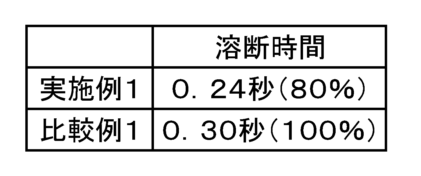
- Example 1 the first side edge portion of the fusible conductor, which is formed thick by coating with a refractory metal, is disposed on the first and second electrodes, and the cut surface of the conductor ribbon The second side edge portion was disposed along a current path extending from the first electrode to the heating element extraction electrode to the second electrode (see FIG. 1). In Comparative Example 1, the first side edge was disposed along the current path, and the second side edge was disposed on the first and second electrodes (see FIG. 7).
- Example 1 In both Example 1 and Comparative Example 1, a power of 35 W was applied and the fusing time was compared. The results are shown in Table 1.
- Example 1 this was formed relatively thin compared to the first side edge portion formed thick with the high melting point metal, and the low melting point metal and the high melting point metal were laminated. Since the second side edge portion is disposed along the current path extending to the first and second electrodes, it can be quickly utilized with less thermal energy and by utilizing the erosion action of the high melting point metal by the low melting point metal. It depends on being able to blow.
- the optimum thickness of the refractory metal layer 13b of the soluble conductor 13 will be described.
- the low melting point metal layer 13a serving as the inner layer is covered with the high melting point metal layer 13b serving as the outer layer.
- the soluble conductor 13 is rapidly eroded by the low melting point metal when the heating element 14 generates heat, and the fusing time can be shortened. Therefore, in the soluble conductor 13, it is preferable to form the refractory metal layer 13b as thin as possible from the viewpoint of fast fusing.
- the fusible conductor 13 is formed as thick as possible from the viewpoint of maintaining the fusing characteristics while enabling the mounting by reflow mounting.
- the refractory metal layer 13b is formed with an optimum film thickness that can achieve both fast fusing during heat generation of the heating element 14, reflow mounting, and maintenance of fusing characteristics.
- the soluble conductor 13 is formed such that the thickness of the refractory metal layer 13b in the main surface portion 25 is 2 ⁇ m or more on each of the front and back sides.
- the fusible conductor 13 erodes the refractory metal layer 13b with the low melting metal even when the protective element 1 is mounted on the circuit board by reflow mounting. Therefore, deformation of the soluble conductor 13 can be prevented. Therefore, the soluble conductor 13 has stable fusing characteristics without variation in fusing time for each product by setting the film thickness of the refractory metal layer 13b to 2 ⁇ m or more regardless of the rating or size.
- the soluble conductor 13 is formed so that the thickness of the refractory metal layer 13b in the main surface portion 25 is 6 ⁇ m or less on each of the front and back sides.
- the fusible conductor 13 quickly corrodes the refractory metal when the heating element 14 generates heat regardless of the rating or size. Can be blown out in a short time.
- the fusible conductor 13 increases the amount of erosion caused by the low melting point metal, so that the fusing time is increased accordingly.
- the fusible conductor 13 can continuously form the high melting point metal layer 13b on the long low melting point metal foil by electrolytic plating. At this time, the soluble conductor 13 can form the refractory metal layer 13b with a desired film thickness by current control.
- samples of soluble conductors with different thicknesses of the high melting point metal layer covering the low melting point metal foil are prepared, and the protective elements formed using these samples are soldered on the circuit board. It was mounted by reflow, and each soluble conductor sample was examined for deformation and fusing. Moreover, electric power was applied to each protection element, and the fusing time of the soluble conductor sample was measured.
- the fusible conductor sample used in the second example uses a Pb-free solder foil having a thickness of 60 ⁇ m as a low melting point metal foil, and Ag plating is performed on the entire surface of the Pb-free solder foil by an electrolytic plating method. A refractory metal layer of ⁇ 7 ⁇ m was formed.
- each soluble conductor sample can form an Ag plating layer with a desired film thickness by controlling the amount of current.
- Each soluble conductor sample is cut across the width direction after electrolytic plating and formed into a predetermined length.
- Example 2 As each soluble conductor sample, in Comparative Example 2, a refractory metal layer having a thickness of 1 ⁇ m on one side was formed. In Example 2, a refractory metal layer having a thickness of 2 ⁇ m on one side was formed. In Example 3, a refractory metal layer having a thickness of 3 ⁇ m on one side was formed. In Example 4, a refractory metal layer having a thickness of 4 ⁇ m on one side was formed. In Example 5, a refractory metal layer having a thickness of 5 ⁇ m on one side was formed. In Example 6, a refractory metal layer having a thickness of 6 ⁇ m on one side was formed. In Example 7, a refractory metal layer having a thickness of 7 ⁇ m on one side was formed.
- Each soluble conductor sample according to Comparative Example 2 and Examples 2 to 7 is disposed on the first and second electrodes with the first side edges formed thick by coating with a refractory metal.
- the second side edge serving as the cut surface of the conductor ribbon is disposed along the current path extending from the first electrode to the heating element extraction electrode to the second electrode, whereby the protective element according to the second embodiment (See FIG. 1). 24 protective elements were prepared for each of the soluble conductors according to Comparative Example 2 and Examples 2 to 7.
- each protection element was mounted on the circuit board by solder reflow.
- the reflow temperature is about 260 ° C.
- the cover member of the protective element was opened, the soluble conductor sample was visually observed, the deformation of the soluble conductor was evaluated, and the melting rate (%) of the soluble conductor was determined.
- a power of 35 W was applied to each protection element, and the fusing time (sec) was compared.
- the melting occurrence rate of the soluble conductor was determined from the number of samples that led to fusing out of 24 samples of each soluble conductor. The results are shown in Table 2 and FIG.
- any sample can be used for the soluble conductor by reflow mounting. There was no significant deformation. Further, in Examples 2 to 6 in which the Ag plating thickness was 2 to 6 ⁇ m, the melting time of the soluble conductor was as short as 0.44 sec or less, and it was possible to sufficiently meet the demand for fast melting.
- Comparative Example 1 in which the Ag plating thickness was 1 ⁇ m, although the fusing time was shortened, 30% of the samples in which the soluble conductor was melted by reflow mounting occurred. This is because the Ag plating layer is too thin, the solder foil is melted by reflow heating, and the Ag plating layer is eroded by the molten solder.
- the Ag plating layer constituting the outer layer of the soluble conductor is preferably formed with a thickness of 2 ⁇ m or more, more preferably 6 ⁇ m or less.
- SYMBOLS 1 Protection element 11 Insulation board
Landscapes
- Fuses (AREA)
- Connection Of Batteries Or Terminals (AREA)
Abstract
Description
本発明が適用された保護素子1は、図1(A)に示すように、絶縁基板11と、絶縁基板11に積層され、絶縁部材15に覆われた発熱体14と、絶縁基板11の両端に形成された第1の電極12(A1)及び第2の電極12(A2)と、絶縁部材15上に発熱体14と重畳するように積層され、発熱体に電気的に接続された発熱体引出電極16と、両端が第1、第2の電極12(A1),12(A2)にそれぞれ接続され、中央部が発熱体引出電極16に接続された可溶導体13とを備える。
可溶導体13は、内層と外層とからなる積層構造体であり、内層となる低融点金属層13aが、外層となる高融点金属層13bによって被覆されている。低融点金属層13aは、特に限定はなく、例えば、Snを主成分とする金属であり、「Pbフリーハンダ」と一般的に呼ばれる材料(たとえば千住金属工業製、M705等)を好適に用いることができる。低融点金属層13aの融点は、必ずしもリフロー炉の温度よりも高い必要はなく、200℃程度で溶融してもよい。高融点金属層13bも、特に限定はなく、例えば、Ag若しくはCu又はこれらのうちのいずれかを主成分とする金属等、リフロー炉によって基板実装を行う場合においても溶融しない高い融点を有する金属を好適に用いることができる。
ここで、図2に示すように、可溶導体13は、主面部25よりも肉厚に形成された一対の第1の側縁部26と、主面部25と同じ厚さに形成された一対の第2の側縁部27とを有する。第1の側縁部26は、相対向して一対設けられ、第2の側縁部27は、第1の側縁部26と略直交して、相対向して一対設けられている。
次いで、可溶導体13の製造工程について説明する。可溶導体13は、低融点金属層13aを構成する低融点金属箔を高融点金属層13bを構成する金属で被覆することにより製造される。低融点金属層箔を高融点金属被覆する工法としては、長尺状の低融点金属箔に連続して高融点金属メッキを施すことができる電解メッキ法が、作業効率上、製造コスト上、有利となる。
次いで、保護素子1の使用方法について説明する。図3に示すように、上述した保護素子1は、例えば、リチウムイオン二次電池のバッテリパック内の回路に実装されて用いられる。
次いで、可溶導体13の高融点金属層13bの最適な厚さについて説明する。上述したように、本発明に係る可溶導体13は、内層となる低融点金属層13aが、外層となる高融点金属層13bによって被覆されている。

Claims (11)
- 絶縁基板と、
発熱体と、
少なくとも上記発熱体を覆う絶縁部材と、
上記発熱体に電気的に接続された発熱体引出電極と、
第1及び第2の電極と、
上記発熱体引出電極から上記第1及び第2の電極にわたって接続され、加熱により、上記第1の電極と上記第2の電極との間の電流経路を溶断する可溶導体とを備え、
上記可溶導体は、主面部よりも肉厚に形成され、相対向する一対の第1の側縁部と、上記第1の側面部よりも薄い厚さに形成され、相対向する一対の第2の側縁部とを有し、上記第2の側縁部が上記発熱体引出電極から上記第1及び第2の電極にわたる電流経路に沿って配設されている保護素子。 - 上記可溶導体は、上記第1の側縁部が高融点金属によって被覆され、上記第2の側縁部には低融点金属及び上記低融点金属の表面を被覆する上記高融点金属が積層されている請求項1記載の保護素子。
- 上記可溶導体は、長尺状に形成された上記低融点金属の箔の表面に、上記高融点金属が被覆された導体リボンを、幅方向に切断することにより形成される請求項2記載の保護素子。
- 上記可溶導体は、上記低融点金属の表面に、電解メッキ法により上記高融点金属が被覆されている請求項2又は3に記載の保護素子。
- 上記第2の側縁部は、上記低融点金属が端面より外方に露出されている請求項2又は請求項3に記載の保護素子。
- 上記可溶導体は、上記第2の側縁部が上記発熱体引出電極に対峙されている請求項5記載の保護素子。
- 上記可溶導体は、上記第1の側縁部が、上記第1及び第2の電極に接続されている請求項1~3のいずれか1項に記載の保護素子。
- 上記可溶導体は、上記第1の側縁部が、上記第1及び第2の電極に接続されている請求項6に記載の保護素子。
- 上記低融点金属は、Pbフリーハンダであり、上記高融点金属は、Ag若しくはCu又はAg若しくはCuを主成分とする金属である請求項1~3のいずれか1項に記載の保護素子。
- 上記可溶導体は、主面部における上記低融点金属の表裏面に積層された上記高融点金属の膜厚が、それぞれ2μm以上である請求項2又は3に記載の保護素子。
- 上記高融点金属の膜厚が6μm以下である請求項10記載の保護素子。
Priority Applications (2)
| Application Number | Priority Date | Filing Date | Title |
|---|---|---|---|
| KR1020167003800A KR102238851B1 (ko) | 2013-08-21 | 2014-08-20 | 보호 소자 |
| CN201480046000.3A CN105474346B (zh) | 2013-08-21 | 2014-08-20 | 保护元件 |
Applications Claiming Priority (2)
| Application Number | Priority Date | Filing Date | Title |
|---|---|---|---|
| JP2013171786A JP6324684B2 (ja) | 2013-08-21 | 2013-08-21 | 保護素子 |
| JP2013-171786 | 2013-08-21 |
Publications (1)
| Publication Number | Publication Date |
|---|---|
| WO2015025883A1 true WO2015025883A1 (ja) | 2015-02-26 |
Family
ID=52483654
Family Applications (1)
| Application Number | Title | Priority Date | Filing Date |
|---|---|---|---|
| PCT/JP2014/071768 Ceased WO2015025883A1 (ja) | 2013-08-21 | 2014-08-20 | 保護素子 |
Country Status (5)
| Country | Link |
|---|---|
| JP (1) | JP6324684B2 (ja) |
| KR (1) | KR102238851B1 (ja) |
| CN (1) | CN105474346B (ja) |
| TW (1) | TWI658486B (ja) |
| WO (1) | WO2015025883A1 (ja) |
Cited By (3)
| Publication number | Priority date | Publication date | Assignee | Title |
|---|---|---|---|---|
| WO2016143353A1 (ja) * | 2015-03-11 | 2016-09-15 | デクセリアルズ株式会社 | ヒューズエレメント及びヒューズ素子 |
| JP2017022009A (ja) * | 2015-07-10 | 2017-01-26 | デクセリアルズ株式会社 | 保護素子、ヒューズ素子 |
| JP2018018835A (ja) * | 2017-11-01 | 2018-02-01 | デクセリアルズ株式会社 | 保護素子、ヒューズ素子 |
Families Citing this family (9)
| Publication number | Priority date | Publication date | Assignee | Title |
|---|---|---|---|---|
| JP6811590B2 (ja) * | 2016-11-10 | 2021-01-13 | デクセリアルズ株式会社 | 保護素子 |
| TW201740605A (zh) * | 2017-01-23 | 2017-11-16 | Pao-Hsuan Chen | 保護元件與二次電池包 |
| TWI690108B (zh) * | 2017-04-06 | 2020-04-01 | 陳葆萱 | 保護元件以及電池包 |
| CN108630834B (zh) * | 2017-03-20 | 2021-09-07 | 陈葆萱 | 复合式保护元件以及电池组 |
| TW201740598A (zh) * | 2017-04-06 | 2017-11-16 | Pao-Hsuan Chen | 電池包及其保護元件 |
| JP7477958B2 (ja) | 2019-10-30 | 2024-05-02 | デクセリアルズ株式会社 | 保護素子および保護回路 |
| JP7349954B2 (ja) * | 2020-04-13 | 2023-09-25 | ショット日本株式会社 | 保護素子 |
| JP7518786B2 (ja) * | 2021-03-09 | 2024-07-18 | デクセリアルズ株式会社 | ヒューズエレメント、ヒューズ素子及び保護素子 |
| CN117912915B (zh) * | 2024-03-15 | 2024-06-18 | 嘉兴模度新能源有限公司 | 复合熔断电连接结构及电池组 |
Citations (3)
| Publication number | Priority date | Publication date | Assignee | Title |
|---|---|---|---|---|
| JPH0463530U (ja) * | 1990-10-09 | 1992-05-29 | ||
| JP2004185960A (ja) * | 2002-12-03 | 2004-07-02 | Kamaya Denki Kk | 回路保護素子とその製造方法 |
| JP2010003665A (ja) * | 2008-05-23 | 2010-01-07 | Sony Chemical & Information Device Corp | 保護素子及び二次電池装置 |
Family Cites Families (4)
| Publication number | Priority date | Publication date | Assignee | Title |
|---|---|---|---|---|
| JP2001057139A (ja) * | 1999-08-18 | 2001-02-27 | Uchihashi Estec Co Ltd | 電子・電気機器用プロテクタ−及びその製造方法 |
| JP2006221919A (ja) * | 2005-02-09 | 2006-08-24 | Uchihashi Estec Co Ltd | 基板型抵抗体付きヒューズ及び電池パック |
| JP5351860B2 (ja) * | 2009-09-04 | 2013-11-27 | 乾坤科技股▲ふん▼有限公司 | 保護装置 |
| JP5656466B2 (ja) * | 2010-06-15 | 2015-01-21 | デクセリアルズ株式会社 | 保護素子、及び、保護素子の製造方法 |
-
2013
- 2013-08-21 JP JP2013171786A patent/JP6324684B2/ja active Active
-
2014
- 2014-08-20 WO PCT/JP2014/071768 patent/WO2015025883A1/ja not_active Ceased
- 2014-08-20 KR KR1020167003800A patent/KR102238851B1/ko active Active
- 2014-08-20 CN CN201480046000.3A patent/CN105474346B/zh active Active
- 2014-08-20 TW TW103128535A patent/TWI658486B/zh active
Patent Citations (3)
| Publication number | Priority date | Publication date | Assignee | Title |
|---|---|---|---|---|
| JPH0463530U (ja) * | 1990-10-09 | 1992-05-29 | ||
| JP2004185960A (ja) * | 2002-12-03 | 2004-07-02 | Kamaya Denki Kk | 回路保護素子とその製造方法 |
| JP2010003665A (ja) * | 2008-05-23 | 2010-01-07 | Sony Chemical & Information Device Corp | 保護素子及び二次電池装置 |
Cited By (4)
| Publication number | Priority date | Publication date | Assignee | Title |
|---|---|---|---|---|
| WO2016143353A1 (ja) * | 2015-03-11 | 2016-09-15 | デクセリアルズ株式会社 | ヒューズエレメント及びヒューズ素子 |
| JP2016170892A (ja) * | 2015-03-11 | 2016-09-23 | デクセリアルズ株式会社 | ヒューズエレメント及びヒューズ素子 |
| JP2017022009A (ja) * | 2015-07-10 | 2017-01-26 | デクセリアルズ株式会社 | 保護素子、ヒューズ素子 |
| JP2018018835A (ja) * | 2017-11-01 | 2018-02-01 | デクセリアルズ株式会社 | 保護素子、ヒューズ素子 |
Also Published As
| Publication number | Publication date |
|---|---|
| JP6324684B2 (ja) | 2018-05-16 |
| TWI658486B (zh) | 2019-05-01 |
| KR102238851B1 (ko) | 2021-04-09 |
| JP2015041491A (ja) | 2015-03-02 |
| CN105474346B (zh) | 2018-01-23 |
| TW201517105A (zh) | 2015-05-01 |
| CN105474346A (zh) | 2016-04-06 |
| KR20160044472A (ko) | 2016-04-25 |
Similar Documents
| Publication | Publication Date | Title |
|---|---|---|
| JP6324684B2 (ja) | 保護素子 | |
| JP6249600B2 (ja) | 保護素子 | |
| JP6437253B2 (ja) | 保護素子及び実装体 | |
| TWI681433B (zh) | 保護元件及電池組 | |
| JP2015111526A (ja) | 保護素子及びヒューズエレメント | |
| JP6621255B2 (ja) | 保護素子、ヒューズ素子 | |
| JP6371118B2 (ja) | 保護素子、及びバッテリパック | |
| CN109937464B (zh) | 保护元件 | |
| JP2024009983A (ja) | 保護素子及びバッテリパック | |
| CN110050323A (zh) | 保护元件 | |
| WO2015072122A1 (ja) | 可溶導体の製造方法 | |
| TWI656554B (zh) | 阻斷元件及阻斷元件電路 | |
| JP6712257B2 (ja) | 保護素子、ヒューズ素子 | |
| JP7443144B2 (ja) | 保護素子及びバッテリパック | |
| JP2016018683A (ja) | 保護素子 | |
| WO2022181652A1 (ja) | 保護素子及びバッテリパック | |
| JP2022142545A (ja) | 保護素子及びバッテリパック | |
| JP2014127270A (ja) | 保護素子 | |
| WO2015107632A1 (ja) | 保護素子 | |
| WO2015107633A1 (ja) | 保護素子、バッテリモジュール |
Legal Events
| Date | Code | Title | Description |
|---|---|---|---|
| WWE | Wipo information: entry into national phase |
Ref document number: 201480046000.3 Country of ref document: CN |
|
| 121 | Ep: the epo has been informed by wipo that ep was designated in this application |
Ref document number: 14837653 Country of ref document: EP Kind code of ref document: A1 |
|
| DPE1 | Request for preliminary examination filed after expiration of 19th month from priority date (pct application filed from 20040101) | ||
| ENP | Entry into the national phase |
Ref document number: 20167003800 Country of ref document: KR Kind code of ref document: A |
|
| NENP | Non-entry into the national phase |
Ref country code: DE |
|
| 122 | Ep: pct application non-entry in european phase |
Ref document number: 14837653 Country of ref document: EP Kind code of ref document: A1 |