WO2015016164A1 - 樹脂組成物及びゲート絶縁膜 - Google Patents
樹脂組成物及びゲート絶縁膜 Download PDFInfo
- Publication number
- WO2015016164A1 WO2015016164A1 PCT/JP2014/069787 JP2014069787W WO2015016164A1 WO 2015016164 A1 WO2015016164 A1 WO 2015016164A1 JP 2014069787 W JP2014069787 W JP 2014069787W WO 2015016164 A1 WO2015016164 A1 WO 2015016164A1
- Authority
- WO
- WIPO (PCT)
- Prior art keywords
- group
- resin composition
- resin
- acid
- compound
- Prior art date
- Legal status (The legal status is an assumption and is not a legal conclusion. Google has not performed a legal analysis and makes no representation as to the accuracy of the status listed.)
- Ceased
Links
Images


Classifications
-
- C—CHEMISTRY; METALLURGY
- C08—ORGANIC MACROMOLECULAR COMPOUNDS; THEIR PREPARATION OR CHEMICAL WORKING-UP; COMPOSITIONS BASED THEREON
- C08L—COMPOSITIONS OF MACROMOLECULAR COMPOUNDS
- C08L29/00—Compositions of homopolymers or copolymers of compounds having one or more unsaturated aliphatic radicals, each having only one carbon-to-carbon double bond, and at least one being terminated by an alcohol, ether, aldehydo, ketonic, acetal or ketal radical; Compositions of hydrolysed polymers of esters of unsaturated alcohols with saturated carboxylic acids; Compositions of derivatives of such polymers
- C08L29/02—Homopolymers or copolymers of unsaturated alcohols
- C08L29/04—Polyvinyl alcohol; Partially hydrolysed homopolymers or copolymers of esters of unsaturated alcohols with saturated carboxylic acids
-
- C—CHEMISTRY; METALLURGY
- C08—ORGANIC MACROMOLECULAR COMPOUNDS; THEIR PREPARATION OR CHEMICAL WORKING-UP; COMPOSITIONS BASED THEREON
- C08K—Use of inorganic or non-macromolecular organic substances as compounding ingredients
- C08K5/00—Use of organic ingredients
- C08K5/04—Oxygen-containing compounds
- C08K5/15—Heterocyclic compounds having oxygen in the ring
- C08K5/151—Heterocyclic compounds having oxygen in the ring having one oxygen atom in the ring
- C08K5/1515—Three-membered rings
-
- C—CHEMISTRY; METALLURGY
- C08—ORGANIC MACROMOLECULAR COMPOUNDS; THEIR PREPARATION OR CHEMICAL WORKING-UP; COMPOSITIONS BASED THEREON
- C08L—COMPOSITIONS OF MACROMOLECULAR COMPOUNDS
- C08L5/00—Compositions of polysaccharides or of their derivatives not provided for in groups C08L1/00 or C08L3/00
-
- C—CHEMISTRY; METALLURGY
- C08—ORGANIC MACROMOLECULAR COMPOUNDS; THEIR PREPARATION OR CHEMICAL WORKING-UP; COMPOSITIONS BASED THEREON
- C08L—COMPOSITIONS OF MACROMOLECULAR COMPOUNDS
- C08L61/00—Compositions of condensation polymers of aldehydes or ketones; Compositions of derivatives of such polymers
- C08L61/04—Condensation polymers of aldehydes or ketones with phenols only
- C08L61/06—Condensation polymers of aldehydes or ketones with phenols only of aldehydes with phenols
-
- H—ELECTRICITY
- H10—SEMICONDUCTOR DEVICES; ELECTRIC SOLID-STATE DEVICES NOT OTHERWISE PROVIDED FOR
- H10D—INORGANIC ELECTRIC SEMICONDUCTOR DEVICES
- H10D30/00—Field-effect transistors [FET]
- H10D30/60—Insulated-gate field-effect transistors [IGFET]
- H10D30/67—Thin-film transistors [TFT]
- H10D30/6729—Thin-film transistors [TFT] characterised by the electrodes
- H10D30/6737—Thin-film transistors [TFT] characterised by the electrodes characterised by the electrode materials
- H10D30/6739—Conductor-insulator-semiconductor electrodes
-
- H—ELECTRICITY
- H10—SEMICONDUCTOR DEVICES; ELECTRIC SOLID-STATE DEVICES NOT OTHERWISE PROVIDED FOR
- H10P—GENERIC PROCESSES OR APPARATUS FOR THE MANUFACTURE OR TREATMENT OF DEVICES COVERED BY CLASS H10
- H10P14/00—Formation of materials, e.g. in the shape of layers or pillars
- H10P14/60—Formation of materials, e.g. in the shape of layers or pillars of insulating materials
- H10P14/68—Organic materials, e.g. photoresists
- H10P14/683—Organic materials, e.g. photoresists carbon-based polymeric organic materials, e.g. polyimides, poly cyclobutene or PVC
-
- C—CHEMISTRY; METALLURGY
- C08—ORGANIC MACROMOLECULAR COMPOUNDS; THEIR PREPARATION OR CHEMICAL WORKING-UP; COMPOSITIONS BASED THEREON
- C08K—Use of inorganic or non-macromolecular organic substances as compounding ingredients
- C08K5/00—Use of organic ingredients
- C08K5/16—Nitrogen-containing compounds
- C08K5/21—Urea; Derivatives thereof, e.g. biuret
-
- C—CHEMISTRY; METALLURGY
- C08—ORGANIC MACROMOLECULAR COMPOUNDS; THEIR PREPARATION OR CHEMICAL WORKING-UP; COMPOSITIONS BASED THEREON
- C08K—Use of inorganic or non-macromolecular organic substances as compounding ingredients
- C08K5/00—Use of organic ingredients
- C08K5/16—Nitrogen-containing compounds
- C08K5/34—Heterocyclic compounds having nitrogen in the ring
- C08K5/3442—Heterocyclic compounds having nitrogen in the ring having two nitrogen atoms in the ring
- C08K5/3445—Five-membered rings
-
- C—CHEMISTRY; METALLURGY
- C08—ORGANIC MACROMOLECULAR COMPOUNDS; THEIR PREPARATION OR CHEMICAL WORKING-UP; COMPOSITIONS BASED THEREON
- C08L—COMPOSITIONS OF MACROMOLECULAR COMPOUNDS
- C08L2203/00—Applications
- C08L2203/20—Applications use in electrical or conductive gadgets
-
- C—CHEMISTRY; METALLURGY
- C08—ORGANIC MACROMOLECULAR COMPOUNDS; THEIR PREPARATION OR CHEMICAL WORKING-UP; COMPOSITIONS BASED THEREON
- C08L—COMPOSITIONS OF MACROMOLECULAR COMPOUNDS
- C08L2205/00—Polymer mixtures characterised by other features
- C08L2205/03—Polymer mixtures characterised by other features containing three or more polymers in a blend
-
- C—CHEMISTRY; METALLURGY
- C08—ORGANIC MACROMOLECULAR COMPOUNDS; THEIR PREPARATION OR CHEMICAL WORKING-UP; COMPOSITIONS BASED THEREON
- C08L—COMPOSITIONS OF MACROMOLECULAR COMPOUNDS
- C08L2312/00—Crosslinking
- C08L2312/04—Crosslinking with phenolic resin
Definitions
- the present invention relates to a resin composition and a gate insulating film. More specifically, the present invention relates to a high dielectric constant, excellent chemical resistance and adhesiveness, and appropriate reduction in adhesiveness even after high-temperature treatment after film formation.
- the present invention relates to a resin composition that provides a resin film that can be easily prevented, and a gate insulating film obtained using the resin composition.
- a thin film transistor is a transistor having a semiconductor layer, a gate electrode, a source electrode, a drain electrode, and a gate insulating film on a substrate, and is roughly classified into a bottom gate type and a top gate type.
- the bottom gate type includes a gate electrode on a substrate and a source electrode and a drain electrode connected to each other by a semiconductor layer with a gate insulating film interposed therebetween.
- the top gate type has a source electrode and a drain electrode in contact with a semiconductor layer on a substrate, and a gate electrode on the gate electrode via a gate insulating film.
- the gate insulating film constituting such a thin film transistor is required to have excellent insulating properties and electrical characteristics.
- the high dielectric constant gate insulating film enables the transistor to be driven at a low voltage, and contributes to low power consumption of the device.
- a photolithography method and an etching method may be used to form the semiconductor layer, the gate electrode, and the source electrode on the insulating film in a predetermined shape.
- the insulating film is required to have chemical resistance.
- a semiconductor layer, a gate electrode, and a source electrode are formed on the gate insulating film formed in this manner. When forming these semiconductor layers, the gate electrode, and the source electrode, Since the processing at high temperature is performed, the gate insulating film is required to maintain high adhesion even after such high temperature processing is performed.
- Patent Document 1 discloses a technique for forming a gate insulating film using polyvinyl phenol (PVP) as a resin for forming such a gate insulating film.
- PVP polyvinyl phenol
- Non-Patent Document 1 discloses a technique for forming a gate insulating film composed of cyanoethyl pullulan and a crosslinking agent having a triazine ring.
- a gate insulating film is exposed to a high temperature after film formation, it is disclosed. Adhesion with the material is significantly reduced.
- the present invention provides a resin composition that provides a resin film having a high dielectric constant, excellent chemical resistance and adhesion, and capable of appropriately preventing a decrease in adhesion when subjected to high-temperature treatment after film formation, Another object of the present invention is to provide a gate insulating film obtained using the resin composition.
- the present inventors have used a resin containing a hydroxyl group and a cyanoalkyl group as a base resin, and a specific epoxy compound, a specific curing agent, The inventors have found that the above object can be achieved by a resin composition obtained by blending a crosslinking agent having a specific alkoxymethyl group-containing structure, and have completed the present invention.
- R 1 and R 2 are alkyl groups having 1 to 20 carbon atoms, and R 1 and R 2 may be the same or different from each other.
- the ratio of the hydroxyl group and the cyanoalkyl group contained in the resin (A) is 30:70 to 2:98 in terms of a molar ratio of “hydroxyl group: cyanoalkyl group”.
- the resin composition which gives the resin film which has a high dielectric constant is excellent in chemical resistance and adhesiveness, and can prevent the fall of adhesiveness at the time of performing a high temperature process after film formation And a gate insulating film obtained using the resin composition.
- FIG. 1 is a cross-sectional view showing an example of a thin film transistor provided with a gate insulating film made of the resin composition according to the present invention.
- FIG. 2 is a diagram showing a method for manufacturing the thin film transistor shown in FIG.
- FIG. 3 is a cross-sectional view showing another example (second example) of a thin film transistor provided with a gate insulating film made of the resin composition according to the present invention.
- FIG. 4 is a cross-sectional view showing another example (third example) of a thin film transistor including a gate insulating film made of the resin composition according to the present invention.
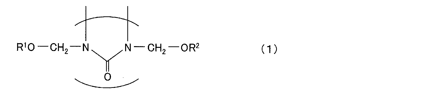
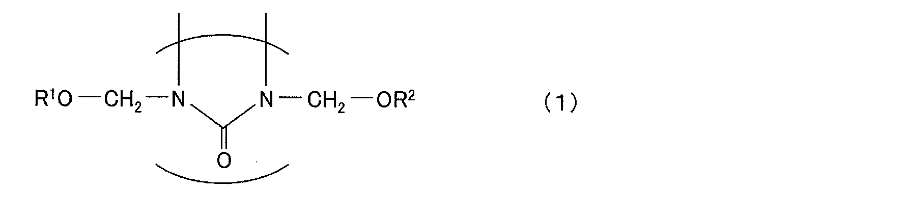
- the resin composition of the present invention comprises a resin (A) containing a hydroxyl group and a cyanoalkyl group, an epoxy compound (B) having two or more epoxy groups in the molecule, two or more hydroxyl groups in the molecule, A curing agent (C) having a value of 150 to 300 mgKOH / g, and a crosslinking agent (D) having a structure represented by the following general formula (1).
- the resin (A) containing a hydroxyl group and a cyanoalkyl group may be any resin containing a hydroxyl group and a cyanoalkyl group.
- hydroxyl group-cyanoalkyl group-containing resin (A) may be any resin containing a hydroxyl group and a cyanoalkyl group.
- a hydroxyl group-containing organic compound having a plurality of hydroxyl groups as a starting material and reacting it with acrylonitrile, a part of the hydroxyl groups contained in the hydroxyl group-containing organic compound is obtained by cyanoalkylation. And the like.
- hydroxyl group-containing organic compound examples include monosaccharides such as glucose, fructose and galactose; disaccharides such as maltose, sucrose and lactose; sugar alcohols such as sorbitol and xylitol; polysaccharides such as cellulose, starch and pullulan; Alkyl celluloses such as carboxymethyl cellulose, hydroxyalkyl celluloses such as hydroxypropyl cellulose, hydroxyethyl cellulose, and dihydroxypropyl cellulose; hydroxyalkylalkyl celluloses such as hydroxypropyl methylcellulose and hydroxyethyl methylcellulose; polysaccharide derivatives such as dihydroxypropyl pullulan; Polyvinylphenol; novolac resin; polyvinylphenol; and the like.
- monosaccharides such as glucose, fructose and galactose
- disaccharides such as maltose, sucrose and lactose
- sugar alcohols such as
- pullulan and polyvinyl alcohol are preferable from the viewpoint that the effect of improving the dielectric constant when the gate insulating film is used is high.
- the cyanoalkyl group for substituting the hydroxyl group-containing organic compound is not particularly limited, but includes a group represented by the general formula: —R—CN (where R is an alkylene group having 2 to 6 carbon atoms).
- R is an alkylene group having 2 to 6 carbon atoms.
- examples include cyanoethyl group, 1-cyanopropyl group, 1-cyanobutyl group, 1-cyanohexyl group and the like.
- a cyanoethyl group is preferable from the viewpoint that introduction into a hydroxyl group-containing organic compound is relatively easy and versatility is high.
- the hydroxyl group-cyanoalkyl group-containing resin (A) used in the present invention may have two or more kinds of cyanoalkyl groups.
- Such a cyanoalkyl group can be introduced by using a corresponding cyano group-containing compound and reacting it with a hydroxyl group-containing organic compound.
- the cyanoalkylation rate can be calculated from the nitrogen content by NMR or elemental analysis.
- the ratio of the hydroxyl group to the cyanoalkyl group in the hydroxyl group-cyanoalkyl group-containing resin (A) used in the present invention is preferably a molar ratio of “hydroxyl group: cyanoalkyl group”, preferably 50:50 to 2:98. More preferably 30:70 to 2:98, and still more preferably 15:85 to 2:98. If the ratio of the hydroxyl group is too low (the cyanoalkylation rate is too high), the chemical resistance of the resulting gate insulating film tends to decrease. On the other hand, if the proportion of hydroxyl groups is too high (the cyanoalkylation rate is too low), the dielectric constant of the resulting gate insulating film tends to decrease.
- epoxy compound (B) (Epoxy compound having two or more epoxy groups in the molecule (B))
- the epoxy compound (B) having two or more epoxy groups in the molecule (hereinafter simply referred to as “epoxy compound (B)”) is not particularly limited as long as it is a compound having two or more epoxy groups.
- epoxy compound either a terminal epoxy group or an alicyclic epoxy group may be sufficient.
- Examples of such epoxy compounds (B) include bisphenol A type epoxy compounds, bisphenol F type epoxy compounds, phenol novolac type epoxy compounds, cresol novolac type epoxy compounds, polyphenol type epoxy compounds, cyclic aliphatic epoxy compounds, glycidyl ethers. Examples thereof include a compound and an epoxy group-containing acrylate polymer. Among these, an epoxy compound having an aromatic hydrocarbon structure is preferable from the viewpoint that the dry etching resistance of the obtained gate insulating film can be further improved, and 2- [4- (2,3-epoxypropoxy) is preferable.
- the epoxy compound which has is more preferable. In addition, these may be used individually by 1 type and may use 2 or more types together.
- epoxy compound (B) examples include bisphenol A type epoxy compounds (trade names “jER828, jER828, jER828EL, jER828XA, jER834, jER1001, jER1002, jER1003, jER1007, jER1009, jER1010, jERYL980U” (and above, Mitsubishi Chemical Corporation).
- Trifunctional epoxy compound having a dicyclopentadiene skeleton (trade name “XD-1000”, manufactured by Nippon Kayaku Co., Ltd.), 1,2-epoxy-4- of 2,2-bis (hydroxymethyl) 1-butanol (2-oxiranyl) cyclohexane adduct
- EHPE3150 2,2-bis (hydroxymethyl) 1-butanol (2-oxiranyl) cyclohexane adduct
- EHPE3150 epoxidized 3-cyclohexene-1,2- Dicarboxylate bis (3-cyclohexenylmethyl) -modified ⁇ -caprolactone
- aliphatic cyclic trifunctional epoxy resin trade name “Epolide GT301”, manufactured by Daicel Chemical Industries
- epoxidized butanetetracarboxylic acid tetrakis (3-cyclo Hexenylmethyl) -modified ⁇ -caprolactone (aliphatic ring having an alicyclic epoxy group) Te
- the content of the epoxy compound (B) in the resin composition of the present invention is preferably 1 to 100 parts by weight, more preferably 5 to 80 parts by weight with respect to 100 parts by weight of the hydroxyl-cyanoalkyl group-containing resin (A). Part, more preferably 10 to 50 parts by weight.
- the curing agent (C) having two or more hydroxyl groups in the molecule and having a hydroxyl value of 150 to 300 mgKOH / g (hereinafter simply referred to as “curing agent (C)”) used in the present invention.
- the compound may be any compound having two or more, and is not particularly limited, but a compound having a phenolic hydroxyl group as a hydroxyl group is preferable.
- the dry etching resistance of the resulting gate insulating film can be improved.
- the curing agent (C) acts as a curing agent for the epoxy compound (B) by reacting with the epoxy group contained in the above-described epoxy compound (B) due to its hydroxyl group, and the crosslinking agent (D) described later. It reacts with the alkoxymethyl group contained in the resin to act as a curing agent for the crosslinking agent (D).
- the curing agent (C) is not particularly limited as long as it is a compound having two or more hydroxyl groups in the molecule and a hydroxyl value in the range of 150 to 300 mgKOH / g.
- phenol, cresol, resorcin, catechol, and the like are examples of phenol, cresol, resorcin, catechol, and the like.
- Acids such as phenols such as bisphenol A, bisphenol F, phenylphenol and aminophenol and / or naphthols such as ⁇ -naphthol, ⁇ -naphthol and dihydroxynaphthalene and compounds having an aldehyde group such as formaldehyde, benzaldehyde and salicylaldehyde Novolac-type phenolic resin obtained by condensation or cocondensation under a catalyst, phenol / aralkyl resin synthesized from phenol and / or naphthol and dimethoxyparaxylene or bis (methoxymethyl) biphenyl, biphenyl Rhenic phenol aralkyl resins, aralkyl phenolic resins such as naphthol aralkyl resins, etc., synthesized by copolymerization of phenols and / or naphthols with dicyclopentadiene, dicyclopentadiene type phenol novolak
- the curing agent (C) may be any compound having a hydroxyl value in the range of 150 to 300 mgKOH / g, but the hydroxyl value is preferably 160 to 250 mgKOH / g, more preferably 175 to 220 mgKOH / g. It is.
- the content of the curing agent (C) in the resin composition of the present invention is preferably 1 to 100 parts by weight, more preferably 3 to 80 parts by weight with respect to 100 parts by weight of the hydroxyl group-cyanoalkyl group-containing resin (A). Part, more preferably 5 to 50 parts by weight.
- Crosslinking agent (D) having a structure represented by the general formula (1)
- the resin composition of the present invention has a structure represented by the following general formula (1) in addition to the above-mentioned hydroxyl-cyanoalkyl group-containing resin (A), epoxy compound (B), and curing agent (C).
- Contains a crosslinking agent (D) hereinafter referred to as “crosslinking agent (D)”.
- R 1 and R 2 are alkyl groups having 1 to 20 carbon atoms. From the viewpoint of solubility in the above-described hydroxyl-cyanoalkyl group-containing resin (A), 1 to 10 carbon atoms are used. Are preferred, and alkyl groups having 1 to 3 carbon atoms are more preferred. R 1 and R 2 may be the same as or different from each other.
- the crosslinking agent (D) used in the present invention is not particularly limited as long as it has a structure represented by the above general formula (1).
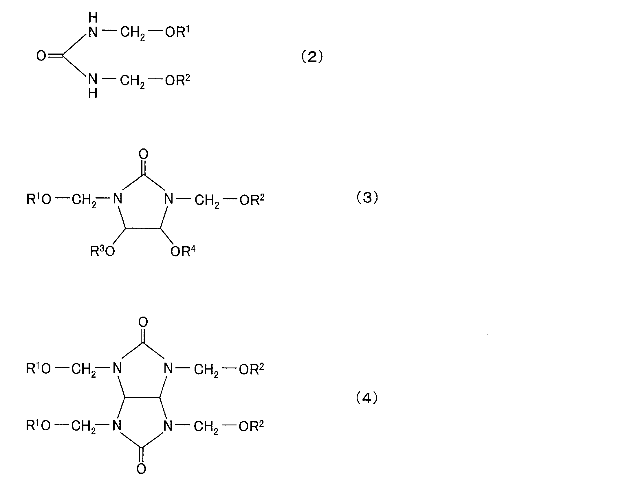
- it is represented by the following general formulas (2) to (4).
- R 1 and R 2 are the same as in the general formula (1).
- R 3 and R 4 And an alkyl group having 1 to 10 carbon atoms, more preferably an alkyl group having 1 to 3 carbon atoms, and in the general formula (3), R 1 , R 2 , R 3 , R 4 may be all or any of the same, or all may be different.
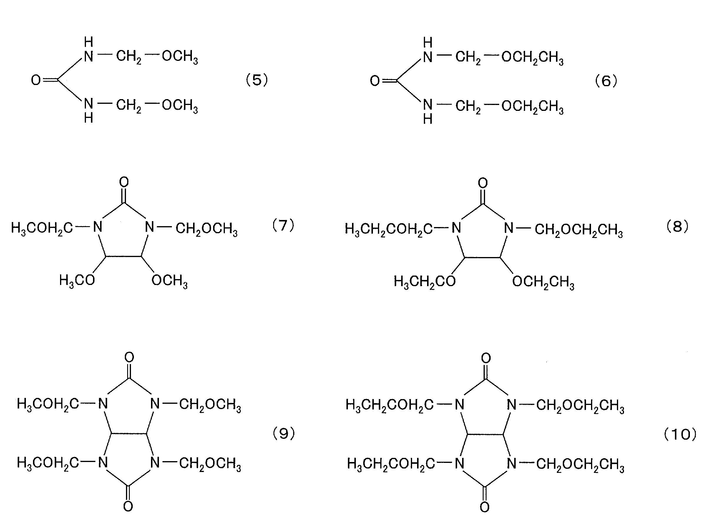
- crosslinking agent (D) used in the present invention include compounds represented by the following formulas (5) to (10), and among these, the effects of the present invention become even more remarkable. Therefore, compounds represented by the following formulas (7) and (9) are preferable, and compounds represented by the following formula (9) are more preferable.
- the content of the crosslinking agent (D) in the resin composition of the present invention is preferably 0.1 to 100 parts by weight, more preferably 1 to 100 parts by weight with respect to 100 parts by weight of the hydroxyl group-cyanoalkyl group-containing resin (A).
- the amount is 50 parts by weight, more preferably 5 to 20 parts by weight.
- the resin composition of the present invention has a phenolic compound (E) (hereinafter simply referred to as “phenolic compound”) having a phenolic hydroxyl group in the molecule and a hydroxyl value of less than 150 mgKOH / g in addition to the above-described components. (E)) ”. ) May be contained.
- phenol compound (E) having a hydroxyl value of less than 150 mgKOH / g, chemical resistance can be further improved while suppressing a decrease in adhesion due to baking after film formation.
- the phenol compound (E) used in the present invention is not particularly limited as long as it has a hydroxyl value of less than 150 mgKOH / g and has a phenolic hydroxyl group, and examples thereof include phenol, cresol, resorcin, catechol.
- Acids such as phenols such as bisphenol A, bisphenol F, phenylphenol and aminophenol and / or naphthols such as ⁇ -naphthol, ⁇ -naphthol and dihydroxynaphthalene and compounds having an aldehyde group such as formaldehyde, benzaldehyde and salicylaldehyde
- phenolic aralate synthesized from a novolak-type phenolic resin, phenols and / or naphthols and dimethoxyparaxylene or bis (methoxymethyl) biphenyl obtained by condensation or cocondensation under a catalyst.
- Dicyclopentadiene-type phenol novolac resin dicyclopentadiene-type phenol resin, dicyclopentadiene synthesized by copolymerization from aralkyl-type phenol resins such as rualkyl resin, biphenylene-type phenol-aralkyl resin, naphthol-aralkyl resin, etc., phenols and / or naphthols
- Dicyclopentadiene type phenolic resin such as pentadiene type naphthol novolak resin, triphenylmethane type phenolic resin, terpene modified phenolic resin, paraxylylene and / or metaxylylene modified phenolic resin, melamine modified phenolic resin, cyclopentadiene modified phenolic resin, biphenyl type phenolic resin And phenol resins obtained by copolymerizing two or more of these. These may be used alone or in combination of two or more.
- the phenol compound (E) may be a compound having a hydroxyl value of less than 150 mgKOH / g, but the hydroxyl value is preferably 50 to 140 mgKOH / g, more preferably 80 to 120 mgKOH / g.
- the content of the phenol compound (E) in the resin composition of the present invention is preferably 0.1 to 100 parts by weight, more preferably 1 to 1 part by weight based on 100 parts by weight of the hydroxyl group-cyanoalkyl group-containing resin (A).
- the amount is 50 parts by weight, more preferably 5 to 20 parts by weight.
- the content of the phenol compound (E) is the total amount of the curing agent (C) described above (that is, the total amount of the phenol compound (E) and the curing agent (C)), and the hydroxyl group-cyanoalkyl group is contained.
- the amount is preferably in the range of 1 to 100 parts by weight with respect to 100 parts by weight of the resin (A), more preferably 5 to 50 parts by weight, still more preferably 10 to 40 parts by weight. .
- the phenol compound (E) acts as a curing agent for the epoxy compound (B) by reacting with the epoxy group contained in the above-described epoxy compound (B) by its hydroxyl group, similarly to the curing agent (C). At the same time, it reacts with an alkoxymethyl group contained in the crosslinking agent (D) described later, thereby acting as a curing agent for the crosslinking agent (D).
- the resin composition of this invention may contain the curing catalyst (F).
- the curing catalyst (F) include a compound having an acidic group or a latent acidic group, and a compound having a basic group or a latent basic group.
- the compound having an acidic group or a latent acidic group is not particularly limited as long as it has an acidic group or a latent acidic group that generates an acid by heating or light, but is preferably an aliphatic compound, an aromatic compound, a complex compound.
- the compound having a basic group or a latent basic group is not particularly limited as long as it has a basic group or a latent basic group that generates a basic group by heating, but is preferably an aliphatic compound, aromatic Group compounds and heterocyclic compounds, more preferably aromatic compounds and heterocyclic compounds.
- the number of acidic groups in the compound having an acidic group is not particularly limited, but those having a total of two or more acidic groups are preferable.
- the acidic groups may be the same as or different from each other.
- the acidic group may be an acidic functional group, and specific examples thereof include strong acidic groups such as sulfonic acid group and phosphoric acid group; weak acidic groups such as carboxy group, thiol group and carboxymethylenethio group; Can be mentioned.
- a carboxy group, a thiol group or a carboxymethylenethio group is preferable, and a carboxy group is particularly preferable.
- these acidic groups those having an acid dissociation constant pKa in the range of 3.5 to 5.0 are preferred.
- the first dissociation constant pKa1 is an acid dissociation constant and the first dissociation constant pKa1 is in the above range.
- BH represents an organic acid
- B ⁇ represents a conjugate base of the organic acid.
- the measuring method of pKa can measure hydrogen ion concentration, for example using a pH meter, and can calculate it from the density
- the compound having an acidic group or a latent acidic group may have a substituent other than the acidic group and the latent acidic group.
- substituents in addition to hydrocarbon groups such as alkyl groups and aryl groups, halogen atoms; alkoxy groups, aryloxy groups, acyloxy groups, heterocyclic oxy groups; substituted with alkyl groups, aryl groups, or heterocyclic groups
- Polar groups having no proton such as amino group, acylamino group, ureido group, sulfamoylamino group, alkoxycarbonylamino group, aryloxycarbonylamino group; alkylthio group, arylthio group, heterocyclic thio group; Examples thereof include a hydrocarbon group substituted with a polar group having no proton.
- the compound having an acidic group include methanoic acid, ethanoic acid, propanoic acid, butanoic acid, pentanoic acid, butanoic acid, pentanoic acid, hexanoic acid, Heptanoic acid, octanoic acid, nonanoic acid, decanoic acid, glycolic acid, glyceric acid, ethanedioic acid (also referred to as “oxalic acid”), propanedioic acid (also referred to as “malonic acid”), butanedioic acid (“succinic acid”) Acid "), pentanedioic acid, hexanedioic acid (also called” adipic acid "), 1,2-cyclohexanedicarboxylic acid, 2-oxopropanoic acid, 2-hydroxybutanedioic acid, 2-hydroxypropanetricarbox
- the latent acidic group may be any group that generates an acidic functional group by light or heating.
- Specific examples thereof include a sulfonium base, a benzothiazolium base, an ammonium base, a phosphonium base, an iodonium salt, and a block carboxylic acid group.
- a sulfonium base is preferable, and for example, a phosphorus hexafluoride-based or antimony hexafluoride-based sulfonium base can be used.
- the basic group may be a basic functional group, and specific examples thereof include an amino group and a nitrogen-containing heterocyclic ring.
- the amino group-containing compound include aliphatic polyamines such as hexamethylene diamine; aromatic polyamines such as 4,4′-diaminodiphenyl ether and diaminodiphenyl sulfone.
- nitrogen-containing heterocyclic compound examples include 2-methylimidazole (product name; 2MZ), 4-methyl-2-ethylimidazole (product name; 2E4MZ), 2-phenylimidazole (product name; 2PZ), and 4-methyl-2-phenylimidazole.
- the compound having a latent basic group may be a compound that generates a basic functional group by light or heating. Specific examples thereof include WPBG-018, WPBG-027, WPBG-082, and WPBG-140 (manufactured by Wako Pure Chemical Industries, Ltd.).
- the content of the curing catalyst (F) in the resin composition of the present invention is preferably 0.01 to 50 parts by weight, more preferably 0.8 parts by weight based on 100 parts by weight of the hydroxyl-cyanoalkyl group-containing resin (A).
- the amount is 1 to 20 parts by weight, more preferably 1 to 10 parts by weight.
- the resin composition of the present invention may further contain a solvent.
- the solvent is not particularly limited, and is known as a resin composition solvent, for example, acetone, methyl ethyl ketone, cyclopentanone, 2-hexanone, 3-hexanone, 2-heptanone, 3-heptanone, 4-heptanone, 2 -Linear ketones such as octanone, 3-octanone, 4-octanone; alcohols such as n-propyl alcohol, isopropyl alcohol, n-butyl alcohol, cyclohexanol; ethylene glycol dimethyl ether, ethylene glycol diethyl ether, dioxane, etc.
- Alcohol ethers such as ethylene glycol monomethyl ether and ethylene glycol monoethyl ether; propyl formate, butyl formate, propyl acetate, butyl acetate, methyl propionate, ethyl propionate Esters such as methyl butyrate, ethyl butyrate, methyl lactate, ethyl lactate; cellosolv esters such as cellosolve acetate, methyl cellosolve acetate, ethyl cellosolve acetate, propyl cellosolve acetate, butyl cellosolve acetate; propylene glycol, propylene glycol monomethyl ether, propylene glycol Propylene glycols such as monomethyl ether acetate, propylene glycol monoethyl ether acetate, propylene glycol monobutyl ether; die such as diethylene glycol monomethyl ether, diethylene glycol monoethyl ether, diethylene glycol monoe
- the content of the solvent is preferably in the range of 10 to 10,000 parts by weight, more preferably 50 to 5000 parts by weight, and still more preferably 100 to 1000 parts by weight with respect to 100 parts by weight of the hydroxyl group-cyanoalkyl group-containing resin (A). It is.
- the solvent is usually removed after forming the gate insulating film.
- the resin composition of the present invention may have an antioxidant, a surfactant, a coupling agent or a derivative thereof, a sensitizer, a light stabilizer, an antifoam, if desired, as long as the effects of the present invention are not inhibited.
- those described in JP2011-75609A can be used as the coupling agent or derivative thereof, the sensitizer, and the light stabilizer.
- antioxidant Although it does not specifically limit as antioxidant, for example, the phenolic antioxidant, phosphorus antioxidant, sulfur antioxidant, amine antioxidant, lactone type oxidation which are used for the usual polymer are used. An inhibitor or the like can be used. By containing an antioxidant, the light resistance and heat resistance of the obtained gate insulating film can be improved.
- phenolic antioxidant conventionally known ones can be used, for example, 2-t-butyl-6- (3-t-butyl-2-hydroxy-5-methylbenzyl) -4-methylphenyl acrylate, 2 , 4-di-t-amyl-6- [1- (3,5-di-t-amyl-2-hydroxyphenyl) ethyl] phenyl acrylate and the like, and JP-A Nos. 63-179953 and 1-168643. Acrylate-based compounds described in the publication No.
- 6- (4-hydroxy-3,5-di-t-butylanilino) -2,4-bis-octylthio-1,3,5-triazine, 6- (4-hydroxy-3,5) -Dimethylanilino) -2,4-bis-octylthio-1,3,5-triazine, 6- (4-hydroxy-3-methyl-5-t-butylanilino) -2,4-bis-octylthio-1, Triazine group-containing phenolic compounds such as 3,5-triazine, 2-octylthio-4,6-bis- (3,5-di-t-butyl-4-oxyanilino) -1,3,5-triazine; Can be used.
- the phosphorus antioxidant is not particularly limited as long as it is usually used in the general resin industry.
- monophosphite compounds are preferable, and tris (nonylphenyl) phosphite, tris (dinonylphenyl) phosphite, tris (2,4-di-t-butylphenyl) phosphite and the like are particularly preferable.
- sulfur-based antioxidant examples include dilauryl 3,3′-thiodipropionate, dimyristyl 3,3′-thiodipropionate, distearyl 3,3′-thiodipropionate, laurylstearyl 3,3 ′.
- -Thiodipropionate pentaerythritol-tetrakis- ( ⁇ -lauryl-thio-propionate), 3,9-bis (2-dodecylthioethyl) -2,4,8,10-tetraoxaspiro [5,5] Undecane or the like can be used.
- antioxidants can be used alone or in combination of two or more.
- the content of the antioxidant in the resin composition of the present invention is preferably 0.1 to 10 parts by weight, more preferably 1 to 10 parts by weight with respect to 100 parts by weight of the hydroxyl-cyanoalkyl group-containing resin (A). 5 parts by weight.
- the content of the antioxidant is in the above range, the light resistance and heat resistance of the obtained gate insulating film can be improved.
- Surfactant is used for the purpose of preventing striations (after coating).
- the surfactant include silicone surfactants, fluorine surfactants, polyoxyalkylene surfactants, methacrylic acid copolymer surfactants, and acrylic acid copolymer surfactants. it can.
- silicone surfactant examples include trade names “SH28PA, SH29PA, SH30PA, ST80PA, ST83PA, ST86PA, SF8416, SH203, SH230, SF8419, SF8422, FS1265, SH510, SH550, SH710, SH8400, SF8410, SH8700, and SH8410.
- fluorosurfactant examples include Fluorinert “FC-430, FC-431” (above, manufactured by Sumitomo 3M), Surflon “S-141, S-145, S-381, S-393” (above, Asahi Glass Co., Ltd.), F-top “EF301, EF303, EF351, EF352” (above, manufactured by Gemco), MegaFac “F171, F172, F173, R-30” (above, manufactured by DIC), etc. .
- polyoxyalkylene surfactant examples include polyoxyethylene alkyl ethers such as polyoxyethylene lauryl ether, polyoxyethylene stearyl ether, polyoxyethylene oleyl ether, polyoxyethylene octylphenyl ether, polyoxyethylene nonylphenyl ether, and the like. And polyethylene glycol dilaurate, polyethylene glycol distearate polyoxyethylene dialkyl esters, and the like. These surfactants can be used alone or in combination of two or more.
- the content of the surfactant in the resin composition of the present invention is preferably 0.01 to 0.5 parts by weight, more preferably 100 parts by weight of the hydroxyl-cyanoalkyl group-containing resin (A). 0.02 to 0.2 parts by weight.
- the content of the surfactant is in the above range, the effect of preventing striation (after the application stripe) can be further enhanced.
- the preparation method of the resin composition of this invention is not specifically limited, What is necessary is just to mix each component which comprises a resin composition by a well-known method.
- the mixing method is not particularly limited, but it is preferable to mix a solution or dispersion obtained by dissolving or dispersing each component constituting the resin composition in a solvent. Thereby, a resin composition is obtained with the form of a solution or a dispersion liquid.
- the method for dissolving or dispersing each component constituting the resin composition in a solvent may be in accordance with a conventional method. Specifically, stirring using a stirrer and a magnetic stirrer, a high-speed homogenizer, a disper, a planetary stirrer, a twin-screw stirrer, a ball mill, a three-roll, etc. can be used. Further, after each component is dissolved or dispersed in a solvent, it may be filtered using, for example, a filter having a pore size of about 0.1 ⁇ m.
- the gate insulating film of the present invention comprises the above-described resin composition of the present invention, and is usually used for a thin film transistor.
- FIG. 1 shows a cross-sectional view of a bottom-gate thin film transistor 1 as an example of a thin film transistor to which the gate insulating film of the present invention is applied.
- the thin film transistor to which the gate insulating film of the present invention is applied is not limited to the thin film transistor having the structure shown in FIG.
- a bottom gate type thin film transistor 1 as an example of a thin film transistor to which the gate insulating film of the present invention is applied includes a gate electrode 3 and a gate made of the above-described resin composition of the present invention on a substrate 2. Insulating film 4, semiconductor layer 5, source electrode 6 and drain electrode 7, and protective layer 8 are provided.
- FIG. 1 shows a single thin film transistor 1, a configuration in which a plurality of thin film transistors 1 are formed on a substrate 2 (for example, an active matrix substrate) may be used.
- the substrate 2 is not particularly limited, and is a flexible substrate made of a flexible plastic such as polycarbonate, polyimide, polyethylene terephthalate, alicyclic olefin polymer, glass substrate such as quartz, soda glass, inorganic alkali glass, silicon wafer, etc.
- the silicon substrate can be mentioned.
- the gate electrode 3 is made of a conductive material.
- conductive materials include platinum, gold, silver, nickel, chromium, copper, iron, tin, antimony lead, tantalum, indium, palladium, tellurium, rhenium, iridium, aluminum, ruthenium, germanium, molybdenum, tungsten, and oxide.
- ITO indium tin oxide
- conductive polymers whose conductivity is improved by doping or the like, such as conductive polyaniline, conductive polypyrrole, and conductive polythiophene (polyethylenedioxythiophene and polystyrenesulfonic acid complex, etc.) can be mentioned.
- the gate insulating film 4 is composed of the above-described resin composition of the present invention, and the above-described resin composition of the present invention is applied to the substrate 2 on which the gate electrode 3 is formed in a predetermined pattern. Accordingly, it is formed by curing after removing the solvent.
- the semiconductor layer 5 is a layer made of an amorphous silicon semiconductor, an organic semiconductor, or an amorphous oxide semiconductor, and among these, the layer made of an amorphous oxide semiconductor from the point that the operational effects of the present invention can be further enhanced. It is particularly preferred that When the semiconductor layer 5 is a layer made of an organic semiconductor, for example, organic compounds represented by pentacene, polythiophene derivatives, polyphenylene vinylene derivatives, polythienylene vinylene derivatives, polyallylamine derivatives, polyacetylene derivatives, acene derivatives, oligothiophenes, etc. A semiconductor material can be used.
- the semiconductor layer 5 When the semiconductor layer 5 is a layer made of an amorphous oxide semiconductor, it can be a sputtered film made of an amorphous oxide semiconductor containing at least one element of In, Ga, and Zn.
- the amorphous oxide semiconductor any element containing at least one element of In, Ga, and Zn may be used.
- the source electrode 6 and the drain electrode 7 are made of a conductive material.
- the conductive material the same material as the gate electrode 3 described above can be used.
- the protective layer 8 is a layer that covers and protects the exposed surface of each component including the substrate 2, the gate electrode 3, the gate insulating film 4, the semiconductor layer 5, the source electrode 6, and the drain electrode 7.
- Examples of the material constituting the protective layer 8 include inorganic films such as SiO 2 , SiON x , SiN x , and Al 2 O 3 , and organic films made of various resins such as acrylic, polyimide, cycloolefin, epoxy, and novolac. It is done.
- the protective layer 8 may be a single layer or a multilayer. Although the thin film transistor 1 according to the present embodiment is configured to include the protective layer 8, it may not be included.
- FIG. 2 is a diagram illustrating a manufacturing process of the thin film transistor 1.
- a layer made of a conductive material for forming the gate electrode 3 is formed on the substrate 2 by sputtering or the like.
- a resist pattern (not shown) is formed by a photolithography method, and a layer made of a conductive material is etched by a wet etching method using the resist pattern as a mask. As shown in FIG. 2A, the gate electrode 3 is formed over the substrate 2.
- the resin composition of the present invention is applied to the substrate 2 on which the gate electrode 3 is formed, the solvent is removed as necessary, and then the gate insulating film is cured. 4 is formed.
- Examples of the method for applying the resin composition of the present invention include various methods such as spraying, spin coating, roll coating, die coating, doctor blade, spin coating, bar coating, and screen printing. Can be adopted.
- the curing temperature (crosslinking temperature) is usually 100 to 300 ° C., preferably 100 to 250 ° C., more preferably 100 to 230 ° C., and the curing time is usually 0.5 to 300 minutes, preferably 1 to 150. Minutes, more preferably 1 to 60 minutes.
- the thickness of the gate insulating film 4 is not particularly limited, but is preferably 100 to 2000 nm, more preferably 100 to 1000 nm, and still more preferably 100 to 500 nm.
- a semiconductor layer 5 is formed on the gate insulating film 4 of the substrate 2 on which the gate electrode 3 and the gate insulating film 4 are formed.
- a layer made of an amorphous oxide semiconductor containing at least one element of In, Ga, and Zn (hereinafter referred to as “amorphous oxide semiconductor layer”) is formed on the gate insulating film 4 by a sputtering method. Is formed over the entire surface of the gate insulating film 4.
- the amorphous oxide semiconductor layer is composed of indium oxide (In 2 O 3 ), gallium oxide (Ga 2 O 3 ), and zinc oxide ( Film formation is performed by DC (Direct Current) sputtering using a target obtained by mixing and sintering equimolar amounts of ZnO). Sputtering can be performed by introducing argon (Ar) gas having a flow rate of 100 to 300 sccm and oxygen (O 2 ) gas having a flow rate of 5 to 20 sccm into the chamber. The substrate temperature at this time is set to 150 to 400 ° C.
- annealing may be performed in an air atmosphere at 200 to 500 ° C. for about 1 to 2 hours.
- a predetermined resist pattern is formed on the surface of the formed amorphous oxide semiconductor layer, the amorphous oxide semiconductor layer is etched by a dry etching method using the resist pattern as a mask, and then the resist pattern is peeled off, whereby FIG. As shown in (C), a semiconductor layer 5 is formed on the gate insulating film 4.
- a source electrode 6 and a drain electrode 7 are formed over the gate insulating film 4 and the semiconductor layer 5. Specifically, first, a layer made of a different conductive material for forming the source electrode 6 and the drain electrode 7 is formed over the entire upper surface of the substrate 2, the gate insulating film 4, and the semiconductor layer 5 by sputtering. To do. Next, a resist pattern corresponding to the shape of the source electrode 6 and the drain electrode 7 is formed on the formed layer made of a conductive material by using a photolithography method. Then, using the formed resist pattern as a mask, a layer made of a conductive material is etched by a dry etching method, and then the resist pattern is peeled off, so that as shown in FIG. A drain electrode 7 is formed.
- a protective layer (passivation film) 8 is formed so as to cover the entire upper surface (exposed surface) of the gate insulating film 4, the semiconductor layer 5, the source electrode 6, and the drain electrode 7, and the bottom as shown in FIG.
- a gate type (channel etch type) thin film transistor 1 is manufactured.
- the protective layer 8 can be formed by using, for example, the plasma CVD method using the above-described materials. As described above, the bottom gate type thin film transistor 1 shown in FIG. 1 is manufactured.
- a gate insulating film used for such an electronic component as the bottom gate type thin film transistor 1 is formed by the above-described resin composition of the present invention.
- a cyanoalkyl group-containing resin (A), an epoxy compound (B), a curing agent (C), and a crosslinking agent (D) has a high dielectric constant, excellent chemical resistance and adhesion, and after film formation It provides a resin film in which the lowering of adhesion when subjected to high temperature treatment is appropriately prevented. Therefore, according to the present invention, by forming the gate insulating film 4 of the thin film transistor 1 shown in FIG. 1 with the resin composition of the present invention, the semiconductor layer 5, the source electrode 6, and the drain electrode are formed on the gate insulating film 4.
- the present invention even when the semiconductor layer 5, the source electrode 6, and the drain electrode 7 are formed, even when firing is performed at a relatively high temperature, the resin obtained using the resin composition of the present invention. Since the gate insulating film 4 made of a film is appropriately prevented from lowering adhesion when subjected to high-temperature treatment after film formation, it is possible to effectively prevent such deterioration in adhesion due to baking. it can.
- the gate insulating film 4 obtained by using the resin composition of the present invention thus effectively prevents a change in film thickness due to deterioration and a decrease in adhesion when a high temperature treatment is performed after film formation, Since a high dielectric constant can be achieved, this makes it possible to improve the performance of electronic components such as the thin film transistor 1 obtained.
- FIG. 3 is a cross-sectional view showing a top gate type thin film transistor 1a provided with a gate insulating film made of the resin composition according to the present invention.
- the same constituent members as those of the thin film transistor 1 described above are denoted by the same reference numerals. The description is omitted.
- 3 includes a source electrode 6, a drain electrode 7, a semiconductor layer 5, a gate insulating film 4 made of the above-described resin composition of the present invention, and a gate electrode 3 on a substrate 2.
- the gate insulating film made of the resin composition according to the present invention can also be suitably used as a gate insulating film of an etch stop layer type thin film transistor 1b as shown in FIG.
- FIG. 4 is a cross-sectional view showing an etch stop layer type thin film transistor 1b provided with a gate insulating film made of the resin composition according to the present invention. The description is omitted.
- the thin film transistor 1b shown in FIG. 4 has the same configuration as the thin film transistor 1 shown in FIG. 1 described above except that an etch stopper 9 is formed so as to cover the channel portion 10. As shown in FIG.
- the thin film transistor 1b has a configuration in which a source electrode 6 and a drain electrode 7 are provided so as to cover the vicinity of the end of the semiconductor layer 5 and the vicinity of the end of the etch stopper 9, respectively.
- FIG. 4 shows a mode in which the protective film 8 is not formed, the protective layer 8 is formed on the source electrode 6, the drain electrode 7, and the etch stopper 9 as in the thin film transistor 1 shown in FIG. It may be formed.
- ⁇ Dielectric constant> The resin composition prepared in each example and each comparative example was spin-coated on a silicon wafer and then pre-baked at 110 ° C. for 2 minutes using a hot plate to form a resin film. Subsequently, the resin film sample which consists of a silicon wafer in which the 500-nm-thick resin film was formed was obtained by heating at 180 degreeC in nitrogen for 1 hour. And the dielectric constant of the resin film was measured at 10 kHz (room temperature) according to JIS C6481 using the obtained resin film sample.
- the adhesion test was performed by the surface-interface cutting method (SAICAS method) described below. That is, a 1 mm width cut was made with a cutter in the resin film portion of the resin film-coated substrate obtained above, and the adhesion-measuring device for the resin film-coated substrate was a Cycus DN- A 20-inch single-crystal diamond cutting blade having a width of 1.0 mm, a rake angle of 20 °, and a relief angle of 10 ° is used as a cutting edge, with a horizontal speed of 0.2 ⁇ m / second and a vertical speed of 0.02 ⁇ m / second.
- SAICAS method surface-interface cutting method
- C Peel strength P is less than 80 N / m
- ⁇ Adhesion after additional firing> Similar to the evaluation of “adhesion after film formation” described above, a substrate with a resin film on which a resin film having a thickness of 2 ⁇ m was formed was obtained. Further, the obtained substrate with a resin film was obtained at 220 ° C. for 1 hour. By heating, the board
- Comparative Examples 1 to 4 A resin composition was prepared in the same manner as in Example 1 except that each compound shown in Table 1 was used in the blending amount shown in Table 1 when preparing the resin composition. Went. The results are shown in Table 1.
- each compound is as follows.
- "Polyvinylphenol” is polyvinylphenol (trade name "Marcalinker MS4P”, manufactured by Maruzen Petrochemical Co., Ltd., a resin containing a hydroxyl group but not a cyanoalkyl group)
- “Epoxy compound (Epicron HP4700)” is an epoxy compound having a naphthalene skeleton (trade name “Epicron HP4700”, manufactured by DIC, epoxy compound (B)).
- Epoxy compound (NC-6000) is 2- [4- (2,3-epoxypropoxy) phenyl] -2- [4- [1,1-bis [4-([2,3-epoxypropoxy] ] Phenyl)] ethyl] phenyl] propane (trade name “NC-6000”, manufactured by Nippon Kayaku Co., Ltd., epoxy compound (B)) ⁇
- Epoxy compound (jERYX8800) is an anthracene dihydride type epoxy resin (trade name "jERYX8800”, manufactured by Mitsubishi Chemical Corporation, epoxy compound (B))
- “Curing agent (MEH-7800)” is a phenol-aralkyl type resin (trade name "MEH-7800", manufactured by Meiwa Kasei Co., Ltd., curing agent (C), hydroxyl value: 175 mgKOH / g)
- Curing agent (MEH-7851) is a phenol-biphenylene type resin (trade name “MEH-
- the resin film comprising the resin composition of the present invention contained has a high dielectric constant, excellent chemical resistance, adhesion after film formation, and adhesion after additional firing, and gate insulation of various electronic components.
- the film was suitable for use as a gate insulating film for a bottom gate type thin film transistor (Examples 1 to 11).
Landscapes
- Chemical & Material Sciences (AREA)
- Health & Medical Sciences (AREA)
- Chemical Kinetics & Catalysis (AREA)
- Medicinal Chemistry (AREA)
- Polymers & Plastics (AREA)
- Organic Chemistry (AREA)
- Compositions Of Macromolecular Compounds (AREA)
- Thin Film Transistor (AREA)
- Epoxy Resins (AREA)
- Formation Of Insulating Films (AREA)
Abstract
Description
〔1〕水酸基及びシアノアルキル基を含有する樹脂(A)と、分子内に2以上のエポキシ基を有するエポキシ化合物(B)と、水酸基を分子内に2以上有し、水酸基価が150~300mgKOH/gである硬化剤(C)と、下記一般式(1)で表される構造を有する架橋剤(D)と、を含有する樹脂組成物、
〔2〕前記樹脂(A)が、水酸基を複数有する水酸基含有有機化合物に含まれる水酸基のうち一部を、シアノアルキル化することにより得られたものである前記〔1〕に記載の樹脂組成物、
〔3〕前記水酸基含有有機化合物が、プルランまたはポリビニルアルコールである前記〔2〕に記載の樹脂組成物、
〔4〕前記エポキシ化合物(B)が、分子内に2以上のエポキシ基を有する芳香族炭化水素構造含有エポキシ化合物である前記〔1〕~〔3〕のいずれかに記載の樹脂組成物、
〔5〕記硬化剤(C)が、前記水酸基としてフェノール性水酸基を有する前記〔1〕~〔4〕のいずれかに記載の樹脂組成物、
〔6〕フェノール性の水酸基を分子内に有し、水酸基価が150mgKOH/g未満であるフェノール化合物(E)をさらに含有する前記〔1〕~〔5〕のいずれかに記載の樹脂組成物、
〔7〕硬化触媒(F)をさらに含有する前記〔1〕~〔6〕のいずれかに記載の樹脂組成物、
〔8〕前記樹脂(A)中に含有される水酸基と、シアノアルキル基との割合が、「水酸基:シアノアルキル基」のモル比で、30:70~2:98である前記〔1〕~〔7〕のいずれかに記載の樹脂組成物、
〔9〕前記架橋剤(D)が、下記一般式(2)~(4)で表される少なくとも一種の化合物である前記〔1〕~〔8〕のいずれかに記載の樹脂組成物、

〔10〕前記〔1〕~〔9〕のいずれかに記載の樹脂組成物を用いて得られるゲート絶縁膜、
が提供される。
本発明の樹脂組成物は、水酸基及びシアノアルキル基を含有する樹脂(A)と、分子内に2以上のエポキシ基を有するエポキシ化合物(B)と、水酸基を分子内に2以上有し、水酸基価が150~300mgKOH/gである硬化剤(C)と、後述する一般式(1)で表される構造を有する架橋剤(D)と、を含有する。
水酸基及びシアノアルキル基を含有する樹脂(A)(以下、「水酸基-シアノアルキル基含有樹脂(A)」とする。)としては、水酸基とシアノアルキル基とを含有する樹脂であればよく、特に限定されないが、例えば、水酸基を複数有する水酸基含有有機化合物を出発原料として用い、これをアクリロニトリルと反応させることにより、水酸基含有有機化合物に含まれる水酸基のうち一部を、シアノアルキル化することにより得られたものなどが挙げられる。
分子内に2以上のエポキシ基を有するエポキシ化合物(B)(以下、単に「エポキシ化合物(B)」とする。)としては、エポキシ基を2以上有する化合物であればよく、特に限定されない。また、エポキシ基としては、末端エポキシ基、脂環式エポキシ基のいずれでもよい。
本発明で用いる、水酸基を分子内に2以上有し、水酸基価が150~300mgKOH/gである硬化剤(C)(以下、単に「硬化剤(C)」とする。)としては、水酸基を2つ以上有する化合物であればよく、特に限定されないが、水酸基としてフェノール性水酸基を有する化合物が好ましい。硬化剤(C)として、エポキシ基と反応する水酸基がフェノール性水酸基である化合物を用いることで、得られるゲート絶縁膜の耐ドライエッチング性を向上させることができる。硬化剤(C)は、その水酸基により、上述したエポキシ化合物(B)に含有されるエポキシ基と反応することで、エポキシ化合物(B)に対する硬化剤として作用するとともに、後述する架橋剤(D)に含有されるアルコキシメチル基と反応することで、架橋剤(D)に対する硬化剤としても作用する。
本発明の樹脂組成物は、上述した水酸基-シアノアルキル基含有樹脂(A)、エポキシ化合物(B)、及び硬化剤(C)に加えて、下記一般式(1)で表される構造を有する架橋剤(D)(以下、「架橋剤(D)」とする。)を含有する。

また、本発明の樹脂組成物は、上述した各成分に加えて、フェノール性の水酸基を分子内に有し、水酸基価が150mgKOH/g未満であるフェノール化合物(E)(以下、単に「フェノール化合物(E))」とする。)を含有していてもよい。水酸基価が150mgKOH/g未満であるフェノール化合物(E)をさらに含有することで、膜形成後の焼成による密着性の低下を抑制しつつ耐薬品性をより高めることができる。
また、本発明の樹脂組成物は、上記各成分に加えて、硬化触媒(F)を含有していてもよい。硬化触媒(F)としては、たとえば、酸性基又は潜在性酸性基を有する化合物、及び塩基性基又は潜在性塩基性基を有する化合物などが挙げられる。酸性基又は潜在性酸性基を有する化合物は、酸性基又は加熱や光により酸を生じる潜在性酸性基を有するものであればよく、特に限定されないが、好ましくは脂肪族化合物、芳香族化合物、複素環化合物であり、さらに好ましくは芳香族化合物、複素環化合物である。塩基性基又は潜在性塩基性基を有する化合物は、塩基性基又は加熱により塩基性基を生じる潜在性塩基性基を有するものであればよく、特に限定されないが、好ましくは脂肪族化合物、芳香族化合物、複素環化合物であり、さらに好ましくは芳香族化合物、複素環化合物である。硬化触媒(F)を配合することで、本発明の樹脂組成物を硬化させる際における硬化に要する加熱エネルギー(加熱時間及び加熱温度)を低減することができる。
酸性基としては、酸性の官能基であればよく、その具体例としては、スルホン酸基、リン酸基等の強酸性基;カルボキシ基、チオール基及びカルボキシメチレンチオ基等の弱酸性基;が挙げられる。これらの中でも、カルボキシ基、チオール基又はカルボキシメチレンチオ基が好ましく、カルボキシ基が特に好ましい。また、これらの酸性基の中でも、酸解離定数pKaが3.5以上5.0以下の範囲にあるものが好ましい。なお、酸性基が2つ以上ある場合は第一解離定数pKa1を酸解離定数とし、第一解離定数pKa1が上記範囲にあるものが好ましい。また、pKaは、希薄水溶液条件下で、酸解離定数Ka=[H3O+][B-]/[BH]を測定し、pKa=-logKaにしたがって、求められる。ここでBHは、有機酸を表し、B-は有機酸の共役塩基を表す。
なお、pKaの測定方法は、例えばpHメータを用いて水素イオン濃度を測定し、該当物質の濃度と水素イオン濃度から算出することができる。
このような置換基としては、アルキル基、アリール基等の炭化水素基のほか、ハロゲン原子;アルコキシ基、アリールオキシ基、アシルオキシ基、ヘテロ環オキシ基;アルキル基又はアリール基又は複素環基で置換されたアミノ基、アシルアミノ基、ウレイド基、スルファモイルアミノ基、アルコキシカルボニルアミノ基、アリールオキシカルボニルアミノ基;アルキルチオ基、アリールチオ基、ヘテロ環チオ基;等のプロトンを有しない極性基、これらのプロトンを有しない極性基で置換された炭化水素基、等を挙げることができる。
塩基性基としては、塩基性の官能基であればよく、その具体例としては、アミノ基、窒素含有複素環が挙げられる。アミノ基含有化合物としては、ヘキサメチレンジアミン等の脂肪族ポリアミン類;4,4’-ジアミノジフェニルエーテル、ジアミノジフェニルスルフォン等の芳香族ポリアミン類が挙げられる。窒素含有複素環化合物としては、2-メチルイミダゾール(品名;2MZ)、4-メチル-2-エチルイミダゾール(品名;2E4MZ)、2-フェニルイミダゾール(品名;2PZ)、4-メチル-2-フェニルイミダゾール(品名;2P4MZ)、1-ベンジル-2-メチルイミダゾール(品名;1B2MZ)、2-エチルイミダゾール(品名;2EZ)、2-イソプロピルイミダゾール(品名;2IZ)、1-シアノエチル-2-メチルイミダゾール(品名;2MZ-CN)、1-シアノエチル-2-エチル-4-メチルイミダゾール(品名;2E4MZ-CN)、1-シアノエチル-2-ウンデシルイミダゾール(品名;C11Z-CN)などがある。
潜在性塩基性基を有する化合物としては、光や加熱により塩基性の官能基を生じる化合物であればよい。その具体例として、WPBG-018、WPBG-027、WPBG-082、WPBG-140(以上、和光純薬工業社製)などが挙げられる。
本発明の樹脂組成物には、さらに、溶剤が含有されていてもよい。溶剤としては、特に限定されず、樹脂組成物の溶剤として公知のもの、例えば、アセトン、メチルエチルケトン、シクロペンタノン、2-ヘキサノン、3-ヘキサノン、2-ヘプタノン、3-ヘプタノン、4-ヘプタノン、2-オクタノン、3-オクタノン、4-オクタノンなどの直鎖のケトン類;n-プロピルアルコール、イソプロピルアルコール、n-ブチルアルコール、シクロヘキサノールなどのアルコール類;エチレングリコールジメチルエーテル、エチレングリコールジエチルエーテル、ジオキサンなどのエーテル類;エチレングリコールモノメチルエーテル、エチレングリコールモノエチルエーテルなどのアルコールエーテル類;ギ酸プロピル、ギ酸ブチル、酢酸プロピル、酢酸ブチル、プロピオン酸メチル、プロピオン酸エチル、酪酸メチル、酪酸エチル、乳酸メチル、乳酸エチルなどのエステル類;セロソルブアセテート、メチルセロソルブアセテート、エチルセロソルブアセテート、プロピルセロソルブアセテート、ブチルセロソルブアセテートなどのセロソルブエステル類;プロピレングリコール、プロピレングリコールモノメチルエーテル、プロピレングリコールモノメチルエーテルアセテート、プロピレングリコールモノエチルエーテルアセテート、プロピレングリコールモノブチルエーテルなどのプロピレングリコール類;ジエチレングリコールモノメチルエーテル、ジエチレングリコールモノエチルエーテル、ジエチレングリコールジメチルエーテル、ジエチレングリコールジエチルエーテル、ジエチレングリコールメチルエチルエーテルなどのジエチレングリコール類;γ-ブチロラクトン、γ-バレロラクトン、γ-カプロラクトン、γ-カプリロラクトンなどの飽和γ-ラクトン類;トリクロロエチレンなどのハロゲン化炭化水素類;トルエン、キシレンなどの芳香族炭化水素類;ジメチルアセトアミド、ジメチルホルムアミド、N-メチルアセトアミドなどの極性溶媒などが挙げられる。これらの溶剤は、単独でも2種以上を組み合わせて用いてもよい。溶剤の含有量は、水酸基-シアノアルキル基含有樹脂(A)100重量部に対して、好ましくは10~10000重量部、より好ましくは50~5000重量部、さらに好ましくは100~1000重量部の範囲である。なお、樹脂組成物に溶剤を含有させる場合には、溶剤は、通常、ゲート絶縁膜形成後に除去されることとなる。
ポリオキシアルキレン系界面活性剤としては、例えば、ポリオキシエチレンラウリルエーテル、ポリオキシエチレンステアリルエーテル、ポリオキシエチレンオレイルエーテル、ポリオキシエチレンオクチルフェニルエーテル、ポリオキシエチレンノニルフェニルエーテル等のポリオキシエチレンアルキルエーテル類、ポリエチレングリコールジラウレート、ポリエチレングリコールジステアレートポリオキシエチレンジアルキルエステル類などを挙げることができる。
これらの界面活性剤は、それぞれ単独で又は2種以上を組み合わせて用いることができる。
混合の方法は特に限定されないが、樹脂組成物を構成する各成分を溶剤に溶解又は分散して得られる溶液又は分散液を混合するのが好ましい。これにより、樹脂組成物は、溶液又は分散液の形態で得られる。
次いで、本発明のゲート絶縁膜について、説明する。本発明のゲート絶縁膜は、上述した本発明の樹脂組成物からなり、通常、薄膜トランジスタに用いられる。
保護層8は、基板2、ゲート電極3、ゲート絶縁膜4、半導体層5、ソース電極6及びドレイン電極7を含む各構成要素の露出表面を被覆して保護する層である。保護層8を構成する材料としては、SiO2、SiONx、SiNx、及びAl2O3などの無機膜、およびアクリル、ポリイミド、シクロオレフィン、エポキシ、ノボラックなどの各種樹脂から成る有機膜が挙げられる。なお、この保護層8は単層でもよいし、多層としてもよい。なお、本実施形態に係る薄膜トランジスタ1は、保護層8を備えて構成したが、備えていなくてもよい。
なお、各特性の定義及び評価方法は、以下のとおりである。
各実施例及び各比較例において作製した樹脂組成物を用いて、樹脂組成物をシリコンウェハ上にスピンコートした後、ホットプレートを用いて110℃で2分間プリベークして、樹脂膜を形成した。次いで、窒素中において180℃で1時間加熱することにより、500nm厚の樹脂膜が形成されたシリコンウェハからなる樹脂膜試料を得た。そして、得られた樹脂膜試料を用いて、JIS C6481に準じて、10kHz(室温)で、樹脂膜の誘電率を測定した。
各実施例及び各比較例において作製した樹脂組成物を、ガラス基板上にスピンコートした後、ホットプレートを用いて110℃で2分間プリベークして、樹脂膜を形成した。次いで、窒素中において180℃で1時間加熱することにより、2μm厚の樹脂膜が形成された樹脂膜付き基板を得た。
A:剥離強度Pが100N/m以上
B:剥離強度Pが80N/m以上、100N/m未満
C:剥離強度Pが80N/m未満
上述した「成膜後の密着性」の評価と同様に、2μm厚の樹脂膜が形成された樹脂膜付き基板を得て、さらに、この得られた樹脂膜付き基板について、220℃、1時間加熱することにより、追加焼成樹脂膜付き基板を得た。そして、得られた追加焼成樹脂膜付き基板を用いた以外は、上述した「成膜後の密着性」の評価と同様に、剥離強度Pを求め、同様の基準にて、追加焼成後の密着性の評価を行った。
上述した「成膜後の密着性」の評価と同様に樹脂膜試料を得て、得られた樹脂膜試料を、アセトン中に、25℃で15分間浸漬し、浸漬前後の樹脂膜の厚みの変化率を測定することで、耐薬品性の評価を行った。なお、浸漬前後の樹脂膜の厚みの変化率は、「浸漬前後の樹脂膜の厚みの変化率(%)=(|浸漬後の樹脂膜の厚み-浸漬前の樹脂膜の厚み|/浸漬前の樹脂膜の厚み)×100」に従って算出した。また、耐薬品性は、以下の基準で評価した。
A:浸漬前後の樹脂膜の厚みの変化率が10%未満
B:浸漬前後の樹脂膜の厚みの変化率が10%以上、20%未満
C:浸漬前後の樹脂膜の厚みの変化率が20%以上
水酸基-シアノアルキル基含有樹脂(A)として、シアノエチル化プルラン(商品名「シアノレジンCR-S」、信越化学工業社製、水酸基:シアノエチル基=10:90(モル比))100部、エポキシ化合物(B)として、テトラキス(グリシジルオキシフェニル)エタン(商品名「jER1031S」、三菱化学社製)20部、硬化剤(C)として、フェノール-アラルキル型樹脂(商品名「KAYAHARD GPH-65」、日本化薬社製、水酸基価:175mgKOH/g)10部、架橋剤(D)として、上記式(9)で示される化合物(商品名「ニカラックMX-270」、三和ケミカル社製)5部、フェノール化合物(E)として、ノボラック型フェノール樹脂(商品名「PAPS-PN4」、旭有機材工業社製、水酸基価:104mgKOH/g)10部、硬化触媒(F)として、PF6 -系スルホニウム塩(商品名「サンエイドSI-110L」、三新化学工業社製)部、3-グリシドキシプロピルトリメトキシシラン(商品名「Z6040」、東レ・ダウコーニング株式会社製、シランカップリング剤)1部、及び溶剤として、γ‐ブチロラクトン60部、プロピレングリコールモノメチルエーテルアセテート40部を混合し、溶解させた後、孔径0.2μmのポリテトラフルオロエチレン製フィルターでろ過して樹脂組成物を調製した。
樹脂組成物を調製する際に、表1に示す各化合物を、表1に示す配合量にて用いた以外は、実施例1と同様にして、樹脂組成物を調製し、同様に試験・評価を行った。結果を表1に示す。
樹脂組成物を調製する際に、表1に示す各化合物を、表1に示す配合量にて用いた以外は、実施例1と同様にして、樹脂組成物を調製し、同様に試験・評価を行った。結果を表1に示す。
・「シアノエチル化ポリビニルアルコール」は、シアノエチル化ポリビニルアルコール(商品名「シアノレジンCR-V」、信越化学工業社製、水酸基:シアノエチル基=15:85(モル比)、水酸基-シアノアルキル基含有樹脂(A))
・「ポリビニルフェノール」は、ポリビニルフェノール(商品名「マルカリンカーMS4P」、丸善石油化学社製、水酸基を含有するが、シアノアルキル基を含有しない樹脂)
・「エポキシ化合物(エピクロンHP4700)」は、ナフタレン骨格を有するエポキシ化合物(商品名「エピクロンHP4700」、DIC社製、エポキシ化合物(B))
・「エポキシ化合物(NC-6000)」は、2-[4-(2,3-エポキシプロポキシ)フェニル]-2-[4-[1,1-ビス[4-([2,3-エポキシプロポキシ]フェニル)]エチル]フェニル]プロパン(商品名「NC-6000」、日本化薬社製、エポキシ化合物(B))
・「エポキシ化合物(jERYX8800)」は、アントラセン ジヒドリド型エポキシ樹脂(商品名「jERYX8800」、三菱化学社製、エポキシ化合物(B))
・「硬化剤(MEH-7800)」は、フェノール-アラルキル型樹脂(商品名「MEH-7800」、明和化成社製、硬化剤(C)、水酸基価:175mgKOH/g)
・「硬化剤(MEH-7851)」は、フェノール-ビフェニレン型樹脂(商品名「MEH-7851」、明和化成社製、硬化剤(C)、水酸基価:220mgKOH/g)
・「式(7)で示される架橋剤(ニカラックMX280)」は、上記式(7)で示される化合物(商品名「ニカラックMX280」、三和ケミカル社製、架橋剤(D))
・「メラミン系架橋剤(サイリンク2000)」は、メラミン系架橋剤(商品名「サイリンク2000」、サイテックインダストリーズ社製、メラミン系架橋剤)
・「メラミン系架橋剤(サイメル350)」は、メラミン系架橋剤(商品名「サイメル350」、サイテックインダストリーズ社製、メラミン系架橋剤)
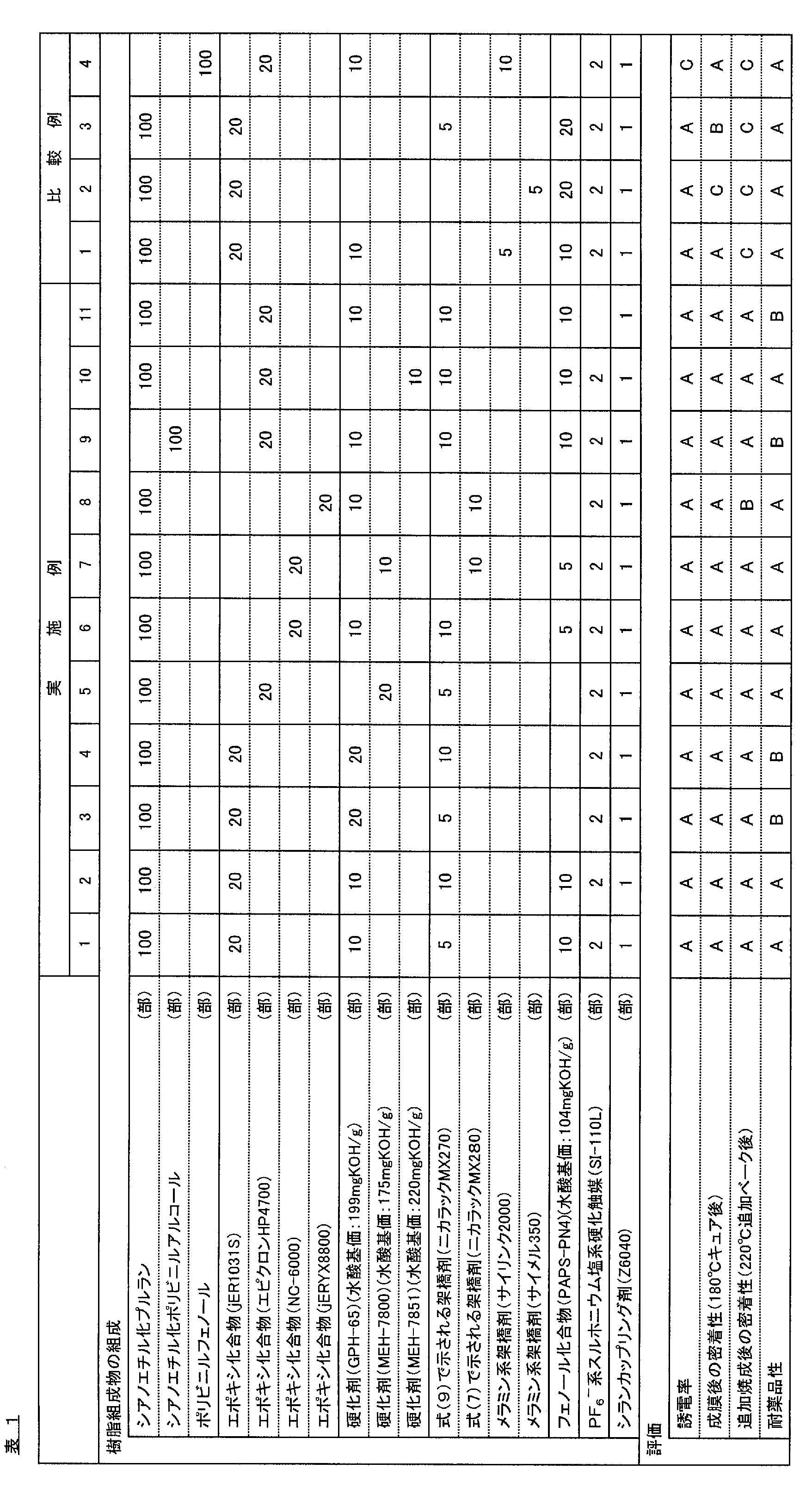
また、硬化剤(C)を配合しなかった場合にも、得られる樹脂膜は、追加焼成後の密着性に劣る結果となった(比較例3)。
さらに、水酸基-シアノアルキル基含有樹脂(A)の代わりに、ポリビニルフェノール(水酸基を含有する一方で、シアノアルキル基を含有しない樹脂)を用いた場合には、得られる樹脂膜は、誘電率が低くなるとともに、追加焼成後の密着性に劣る結果となった(比較例4)。
2…基板
3…ゲート電極
4…ゲート絶縁膜
5…半導体層
6…ソース電極
7…ドレイン電極
8…保護層
Claims (10)
- 水酸基及びシアノアルキル基を含有する樹脂(A)と、
分子内に2以上のエポキシ基を有するエポキシ化合物(B)と、
水酸基を分子内に2以上有し、水酸基価が150~300mgKOH/gである硬化剤(C)と、
下記一般式(1)で表される構造を有する架橋剤(D)と、を含有する樹脂組成物。

- 前記樹脂(A)が、水酸基を複数有する水酸基含有有機化合物に含まれる水酸基のうち一部を、シアノアルキル化することにより得られたものである請求項1に記載の樹脂組成物。
- 前記水酸基含有有機化合物が、プルランまたはポリビニルアルコールである請求項2に記載の樹脂組成物。
- 前記エポキシ化合物(B)が、分子内に2以上のエポキシ基を有する芳香族炭化水素構造含有エポキシ化合物である請求項1~3のいずれかに記載の樹脂組成物。
- 前記硬化剤(C)が、前記水酸基としてフェノール性水酸基を有する請求項1~4のいずれかに記載の樹脂組成物。
- フェノール性の水酸基を分子内に有し、水酸基価が150mgKOH/g未満であるフェノール化合物(E)をさらに含有する請求項1~5のいずれかに記載の樹脂組成物。
- 硬化触媒(F)をさらに含有する請求項1~6のいずれかに記載の樹脂組成物。
- 前記樹脂(A)中に含有される水酸基と、シアノアルキル基との割合が、「水酸基:シアノアルキル基」のモル比で、50:50~2:98である請求項1~7のいずれかに記載の樹脂組成物。
- 前記架橋剤(D)が、下記一般式(2)~(4)で表される少なくとも一種の化合物である請求項1~8のいずれかに記載の樹脂組成物。
- 請求項1~9のいずれかに記載の樹脂組成物を用いて得られるゲート絶縁膜。
Priority Applications (4)
| Application Number | Priority Date | Filing Date | Title |
|---|---|---|---|
| JP2015529558A JP6354762B2 (ja) | 2013-07-31 | 2014-07-28 | 樹脂組成物及びゲート絶縁膜 |
| US14/907,037 US9617408B2 (en) | 2013-07-31 | 2014-07-28 | Resin composition and gate insulating film |
| KR1020167001682A KR20160036558A (ko) | 2013-07-31 | 2014-07-28 | 수지 조성물 및 게이트 절연막 |
| CN201480039193.XA CN105378902B (zh) | 2013-07-31 | 2014-07-28 | 树脂组合物及栅极绝缘膜 |
Applications Claiming Priority (2)
| Application Number | Priority Date | Filing Date | Title |
|---|---|---|---|
| JP2013-158520 | 2013-07-31 | ||
| JP2013158520 | 2013-07-31 |
Publications (1)
| Publication Number | Publication Date |
|---|---|
| WO2015016164A1 true WO2015016164A1 (ja) | 2015-02-05 |
Family
ID=52431697
Family Applications (1)
| Application Number | Title | Priority Date | Filing Date |
|---|---|---|---|
| PCT/JP2014/069787 Ceased WO2015016164A1 (ja) | 2013-07-31 | 2014-07-28 | 樹脂組成物及びゲート絶縁膜 |
Country Status (6)
| Country | Link |
|---|---|
| US (1) | US9617408B2 (ja) |
| JP (1) | JP6354762B2 (ja) |
| KR (1) | KR20160036558A (ja) |
| CN (1) | CN105378902B (ja) |
| TW (1) | TW201512293A (ja) |
| WO (1) | WO2015016164A1 (ja) |
Cited By (1)
| Publication number | Priority date | Publication date | Assignee | Title |
|---|---|---|---|---|
| JP2019060960A (ja) * | 2017-09-25 | 2019-04-18 | 住友ベークライト株式会社 | 感光性樹脂組成物、感光性樹脂フィルム、半導体装置および電子機器 |
Citations (3)
| Publication number | Priority date | Publication date | Assignee | Title |
|---|---|---|---|---|
| WO2006104069A1 (ja) * | 2005-03-28 | 2006-10-05 | Pioneer Corporation | ゲート絶縁膜、有機トランジスタ、有機el表示装置の製造方法、ディスプレイ |
| WO2009133843A1 (ja) * | 2008-04-28 | 2009-11-05 | 日本ゼオン株式会社 | 感放射線樹脂組成物、積層体及びその製造方法ならびに半導体デバイス |
| JP2010067817A (ja) * | 2008-09-11 | 2010-03-25 | Ricoh Co Ltd | 有機電界効果トランジスタ |
Family Cites Families (4)
| Publication number | Priority date | Publication date | Assignee | Title |
|---|---|---|---|---|
| US7252733B2 (en) * | 2004-05-04 | 2007-08-07 | Eastman Kodak Company | Polarizer guarded cover sheet with adhesion promoter |
| US7399376B2 (en) * | 2004-05-04 | 2008-07-15 | Eastman Kodak Company | Polarizing plate laminated with an improved glue composition and a method of manufacturing the same |
| JP2010056115A (ja) | 2008-08-26 | 2010-03-11 | Konica Minolta Holdings Inc | ゲート絶縁膜の形成方法、有機薄膜トランジスタの製造方法および有機薄膜デバイス |
| JP2014165415A (ja) * | 2013-02-27 | 2014-09-08 | Nippon Zeon Co Ltd | 樹脂組成物及びゲート絶縁膜 |
-
2014
- 2014-07-28 KR KR1020167001682A patent/KR20160036558A/ko not_active Withdrawn
- 2014-07-28 JP JP2015529558A patent/JP6354762B2/ja active Active
- 2014-07-28 US US14/907,037 patent/US9617408B2/en not_active Expired - Fee Related
- 2014-07-28 WO PCT/JP2014/069787 patent/WO2015016164A1/ja not_active Ceased
- 2014-07-28 CN CN201480039193.XA patent/CN105378902B/zh not_active Expired - Fee Related
- 2014-07-30 TW TW103125963A patent/TW201512293A/zh unknown
Patent Citations (3)
| Publication number | Priority date | Publication date | Assignee | Title |
|---|---|---|---|---|
| WO2006104069A1 (ja) * | 2005-03-28 | 2006-10-05 | Pioneer Corporation | ゲート絶縁膜、有機トランジスタ、有機el表示装置の製造方法、ディスプレイ |
| WO2009133843A1 (ja) * | 2008-04-28 | 2009-11-05 | 日本ゼオン株式会社 | 感放射線樹脂組成物、積層体及びその製造方法ならびに半導体デバイス |
| JP2010067817A (ja) * | 2008-09-11 | 2010-03-25 | Ricoh Co Ltd | 有機電界効果トランジスタ |
Cited By (1)
| Publication number | Priority date | Publication date | Assignee | Title |
|---|---|---|---|---|
| JP2019060960A (ja) * | 2017-09-25 | 2019-04-18 | 住友ベークライト株式会社 | 感光性樹脂組成物、感光性樹脂フィルム、半導体装置および電子機器 |
Also Published As
| Publication number | Publication date |
|---|---|
| CN105378902B (zh) | 2017-10-13 |
| JPWO2015016164A1 (ja) | 2017-03-02 |
| KR20160036558A (ko) | 2016-04-04 |
| JP6354762B2 (ja) | 2018-07-11 |
| CN105378902A (zh) | 2016-03-02 |
| TW201512293A (zh) | 2015-04-01 |
| US9617408B2 (en) | 2017-04-11 |
| US20160160012A1 (en) | 2016-06-09 |
Similar Documents
| Publication | Publication Date | Title |
|---|---|---|
| US10822449B2 (en) | Low temperature curing composition, cured film formed therefrom, and electronic device having cured film | |
| TWI689561B (zh) | 樹脂組合物、樹脂膜及電子元件 | |
| US20140154627A1 (en) | Negative type photosensitive resin composition, resin film, and electronic device | |
| JP5640864B2 (ja) | ネガ型感光性樹脂組成物および電子部品 | |
| JP6477477B2 (ja) | 感放射線樹脂組成物および電子部品 | |
| CN102640268A (zh) | 半导体元件基板的制造方法 | |
| CN102668046B (zh) | 半导体元件基板 | |
| US20160297181A1 (en) | Laminate | |
| JP6304044B2 (ja) | 感放射線樹脂組成物および電子部品 | |
| JP2013187279A (ja) | 平坦化膜及びそれを備える電子部品 | |
| JP6354762B2 (ja) | 樹脂組成物及びゲート絶縁膜 | |
| JP2014165415A (ja) | 樹脂組成物及びゲート絶縁膜 | |
| JP6164218B2 (ja) | 薄膜トランジスタ | |
| JP6816761B2 (ja) | 樹脂組成物、樹脂膜、及び電子部品 | |
| JP6079277B2 (ja) | 感放射線樹脂組成物及び電子部品 | |
| JP2011071424A (ja) | 薄膜トランジスタ |
Legal Events
| Date | Code | Title | Description |
|---|---|---|---|
| 121 | Ep: the epo has been informed by wipo that ep was designated in this application |
Ref document number: 14831826 Country of ref document: EP Kind code of ref document: A1 |
|
| ENP | Entry into the national phase |
Ref document number: 2015529558 Country of ref document: JP Kind code of ref document: A |
|
| ENP | Entry into the national phase |
Ref document number: 20167001682 Country of ref document: KR Kind code of ref document: A |
|
| WWE | Wipo information: entry into national phase |
Ref document number: 14907037 Country of ref document: US |
|
| NENP | Non-entry into the national phase |
Ref country code: DE |
|
| 122 | Ep: pct application non-entry in european phase |
Ref document number: 14831826 Country of ref document: EP Kind code of ref document: A1 |