WO2015005032A1 - 受信回路及び送信回路、並びに、通信システム及び通信方法 - Google Patents
受信回路及び送信回路、並びに、通信システム及び通信方法 Download PDFInfo
- Publication number
- WO2015005032A1 WO2015005032A1 PCT/JP2014/064939 JP2014064939W WO2015005032A1 WO 2015005032 A1 WO2015005032 A1 WO 2015005032A1 JP 2014064939 W JP2014064939 W JP 2014064939W WO 2015005032 A1 WO2015005032 A1 WO 2015005032A1
- Authority
- WO
- WIPO (PCT)
- Prior art keywords
- signal
- transmission
- circuit
- reference signal
- transmission path
- Prior art date
Links
Images


Classifications
-
- H—ELECTRICITY
- H04—ELECTRIC COMMUNICATION TECHNIQUE
- H04B—TRANSMISSION
- H04B3/00—Line transmission systems
- H04B3/52—Systems for transmission between fixed stations via waveguides
Definitions
- the present disclosure relates to a reception circuit and a transmission circuit, a communication system, and a communication method.
- Non-Patent Documents 1 and 2 As a means of communication between various devices such as electronic devices, information processing devices, and semiconductor devices, and communication between circuit boards in one device (device), information is modulated and transmitted in the millimeter wave band. Communication systems have been proposed (see, for example, Non-Patent Documents 1 and 2).
- P.Pursula, et.al "Millimeter-Wave Identification-A New Short Radio System for Low-Power High Data-Rate Application,” IEEE TRANSACTIONS ON MICROWAVE THEORY AND TECHNIQUES, VOL.56, NO.10, OCTOBER 2008
- P.Pursula, et.al "60-GHz Millimeter-Wave Identification Identification Reader Reader 90-nm CMOS and LTCC IEEE IEEE TRANSACTIONS ON ON MICROWAVE THEORY AND AND TECHNIQUES, VOL.59, NO.4, APRIL 2011
- Non-Patent Documents 1 and 2 above all transmit signals in free space. Therefore, since the radio waves are spread, the efficiency is low, and there is a problem of interference with other communications. In order to avoid interference with other communications, since a usable band is limited, a wideband signal cannot be used.
- An object of the present disclosure is to provide a reception circuit and a transmission circuit, a communication system, and a communication method that are excellent in transmission efficiency, can use a wideband signal without worrying about interference with other communications. .
- a receiving circuit of the present disclosure includes: A reference signal generation unit that generates a high-frequency reference signal and transmits the signal to a transmission circuit through a signal transmission path that transmits the radio wave while confining the radio wave in the transmission path; A transmission data restoring unit that receives the reference signal that is modulated based on the transmission data in the transmission circuit and is returned through the signal transmission path, and restores the transmission data;
- a modulation unit that modulates a high-frequency reference signal transmitted from a receiving circuit through a signal transmission path that transmits the radio wave while confining the radio wave in the transmission path, and returns the modulated signal to the receiving circuit through the signal transmission path,
- a communication system of the present disclosure includes: A transmission circuit for transmitting transmission data; A receiving circuit for generating a high-frequency reference signal; A signal transmission path for transmitting radio waves while confining radio waves in the transmission path between the transmission circuit and the reception circuit; With The transmission circuit modulates the reference signal transmitted from the reception circuit through the signal transmission path based on the transmission data, and returns to the reception circuit through the signal transmission path. The receiving circuit receives the reference signal returned from the transmitting circuit through the signal transmission path, and restores the transmission data.
- the communication method of the present disclosure for achieving the above object is as follows.
- the high-frequency reference signal generated in the receiving circuit is transmitted to the transmitting circuit through the signal transmission path that transmits the radio wave while confining the radio wave in the transmission path.
- a reference signal transmitted from the receiving circuit through the signal transmission path is modulated based on transmission data, and returned to the receiving circuit through the signal transmission path.
- a reference signal returned from the transmission circuit through the signal transmission path is received, and the transmission data is restored.
- the transmission circuit since communication is performed between the receiving circuit and the transmitting circuit through a signal transmission path that transmits radio waves while confining the radio wave in the transmission path, the transmission circuit is excellent in transmission efficiency and does not mind interference with other communications. Wideband signals can be used.
- the effect described in this specification is an illustration to the last, Comprising: It is not limited to this, There may be an additional effect.
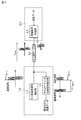
- FIG. 1A is a block diagram illustrating an exemplary configuration of a communication system to which the technology of the present disclosure is applied
- FIG. 1B is a block diagram illustrating an exemplary configuration of a reception circuit and a transmission circuit in the communication system.
- FIG. 2 is a block diagram illustrating a configuration example of a reception circuit and a transmission circuit in the communication system according to the first embodiment.
- FIG. 3 is a block diagram illustrating a configuration example of a reception circuit and a transmission circuit in the communication system according to the second embodiment.
- 4A is a timing waveform diagram illustrating a transmission example # 1 of a millimeter wave reference signal
- FIG. 4B is a timing waveform diagram illustrating a transmission example # 2 of a millimeter wave reference signal.
- FIG. 1A is a block diagram illustrating an exemplary configuration of a communication system to which the technology of the present disclosure is applied
- FIG. 1B is a block diagram illustrating an exemplary configuration of a reception circuit and a transmission circuit in the
- FIG. 5 is a block diagram illustrating a configuration example of a reception circuit and a transmission circuit in the communication system according to the third embodiment.
- FIG. 6 is a block diagram illustrating a configuration example of the reception circuit and the transmission circuit in the communication system according to the fourth embodiment.
- FIG. 7 is a block diagram illustrating a configuration example of the reception circuit and the transmission circuit in the communication system according to the fifth embodiment.
- FIG. 8 is a block diagram illustrating a configuration example of the reception circuit and the transmission circuit in the communication system according to the sixth embodiment.
- FIG. 9A is a configuration diagram showing an outline of a configuration of a system used for verification of millimeter wave transmission by a millimeter wave cable.
- FIG. 9B is a diagram when the termination condition of the millimeter wave cable is switched to SHORT / OPEN. It is a figure which shows a frequency-amplitude characteristic.
- FIG. 10A is a diagram showing time-amplitude characteristics when the termination of the millimeter wave cable is SHORT
- FIG. 10B is a diagram showing time-amplitude characteristics when the termination of the millimeter wave cable is OPEN.
- FIG. 11A is a perspective view showing a coupling portion between the termination of the millimeter wave cable and the termination condition variable portion
- FIG. 11B is a plan view showing the coupling portion
- FIG. 11C shows the coupling portion. It is a side view including a partial cross section.
- FIG. 12 is a circuit diagram illustrating an example of a circuit configuration of the termination condition variable unit including the termination structure of the millimeter wave cable.
- Example 3 (example in which the reference signal is a continuous carrier wave) 3-4.
- Example 4 (Example in which bidirectional transmission is performed with one millimeter wave cable) 3-5.
- Example 5 (Example of bidirectional communication by combination of BPSK transmission and reflection transmission) 3-6.
- Example 6 (example of combining pulse BPSK modulation and time gating) 3-7. Verification of millimeter wave transmission using millimeter wave cable 3-8. Specific example of variable end condition
- a communication system that transmits electromagnetic waves, particularly high-frequency signals such as microwaves, millimeter waves, and terahertz waves, through a signal transmission path is used to transmit signals between various devices such as electronic devices, information processing devices, and semiconductor devices. It is suitable for transmission and transmission of signals between circuit boards in one device (equipment).
- a signal transmission path for transmitting a high-frequency signal has a function as a cable for connecting between devices and between circuit boards.
- a signal transmission path that transmits a radio wave while confining it in the transmission path can be configured by a waveguide or a waveguide.
- the waveguide may have a structure composed of a hollow waveguide, a structure composed of a dielectric waveguide, or a dielectric conductor in which a dielectric is filled in the tube.
- the structure which consists of a wave tube may be sufficient.
- the electromagnetic wave propagates in the dielectric while forming an electromagnetic field corresponding to the wavelength (frequency) or the like.
- the waveguide is made of a dielectric line or the like.
- the reception circuit includes a signal separation unit that separates the reference signal returned from the transmission circuit from the reference signal transmitted to the transmission circuit It can be.
- the signal separation unit can be configured to temporally separate the reference signal transmitted to the transmission circuit and the reference signal returned from the transmission circuit.
- the reference signal generator receives the reference signal returned from the transmitting circuit and then receives the next reference signal. Can be configured to transmit. Alternatively, the reference signal can be generated at a periodic interval that does not overlap with the reference signal returned from the transmission circuit. Alternatively, the reference signal can be transmitted to the transmission circuit as a continuous signal (continuous carrier wave).
- the transmission circuit is configured by changing the termination condition of the signal transmission path based on the transmission data. It can be configured to modulate the signal.
- FIG. 1A is a block diagram illustrating an exemplary configuration of a communication system to which the technology of the present disclosure is applied
- FIG. 1B is a block diagram illustrating an exemplary configuration of a reception circuit and a transmission circuit in the communication system.
- a communication system 1 includes a receiving circuit (receiving unit / receiver) 10, a transmitting circuit (transmitting unit / transmitter) 20, and a receiving circuit 10 and a transmitting circuit 20. It has the structure which has the signal transmission path 30 which transmits a high frequency signal between.
- the reception circuit 10 is provided in the first communication device (electronic device) 100
- the transmission circuit 20 is provided in the second communication device (electronic device) 200.
- the reception circuit 10 and the transmission circuit 20 are arranged within a predetermined range, as shown in FIG. 1A, separate communication devices (electronic devices), that is, the first communication device 100 and the second communication device are used.
- the receiving circuit 10 and the transmitting circuit 20 may be arranged on separate circuit boards in one electronic device. In the case of this form, one circuit board corresponds to the first communication device 100 and the other circuit board corresponds to the second communication device 200.
- the receiving circuit 10 and the transmitting circuit 20 are arranged on separate semiconductor chips in one electronic device.
- one semiconductor chip corresponds to the first communication device 100 and the other semiconductor chip corresponds to the second communication device 200.
- a configuration in which the receiving circuit 10 and the transmitting circuit 20 are arranged in different circuit portions on the same circuit board is conceivable.
- one circuit unit corresponds to the first communication device 100 and the other circuit unit corresponds to the second communication device 200.
- the first communication device 100 and the second communication device 200 for example, the following combinations can be considered.
- the combinations exemplified below are only examples, and are not limited to these combinations.
- the millimeter wave communication can take a wide communication band, it is easy to increase the data rate.
- the frequency used for transmission can be separated from the frequency of other baseband signal processing, and interference between the millimeter wave and the frequency of the baseband signal hardly occurs.
- the millimeter wave band has a short wavelength, the waveguide structure determined according to the wavelength can be made small. In addition, electromagnetic shielding is easy because the distance attenuation is large and the diffraction is small.
- the stability of a carrier wave has strict regulations to prevent interference and the like.
- a millimeter wave in millimeter wave communication (transmission) that modulates and transmits information in the millimeter wave band, a millimeter wave can be realized with a CMOS device that has a generator (oscillator) that generates a millimeter wave reference signal. Therefore, it is necessary to configure the device by a fine high-speed process that can be operated at a high cost.
- high-speed transmission is required in the forward direction for transmitting image signals, but control signals are transmitted in the reverse direction, so low-speed transmission may be sufficient. Many. In such a case, if the millimeter wave is used in the reverse direction, the power consumption increases. In order to reduce power consumption, it is necessary to separately prepare a communication means for low-speed transmission.
- the communication system 1 according to this application example employs a configuration in which a generation unit (oscillator) that generates a millimeter-wave reference signal is not provided on the transmission circuit 20 side by using a load modulation technique. . That is, as shown in FIG. 1B, in the communication system 1 according to this application example, the technology of load modulation is applied to the reception circuit 10 and the transmission circuit 20.
- a generation unit oscillator
- the communication system having the transmission circuit 20 can reduce power consumption and simplify the system configuration.
- the millimeter wave transmission circuit 20 can be realized by a CMOS process (process before 0.13 ⁇ m) at a relatively low speed and at a low cost.
- efficient reflected wave communication using a broadband pulse signal that is, a millimeter-wave reference signal
- the signal transmission path is composed of a waveguide or a waveguide, and transmits radio waves (millimeter waves) while confining them in the transmission path (inside the pipe). Since the signal transmission path for transmitting the millimeter wave has a function as a cable for connecting the receiving circuit 10 and the transmitting circuit 20, it may be hereinafter referred to as a millimeter wave cable 30.
- the transmission circuit 20 modulates the millimeter wave reference signal transmitted from the reception circuit 10 through the millimeter wave cable 30 based on the transmission data, and returns the modulated signal to the reception circuit 10 through the millimeter wave cable 30.
- the receiving circuit 10 transmits a millimeter-wave reference signal to the transmission circuit 20 through the millimeter-wave cable 30, and a millimeter-wave reference signal (modulated signal / reflected signal) returned from the transmission circuit 20 through the millimeter-wave cable 30. Receive and restore transmitted data.
- the signal transmission path (propagation path) between the reception circuit 10 and the transmission circuit 20.
- a millimeter wave cable 30 that transmits radio waves while confining them in the transmission path is used.
- the transmission efficiency can be increased and the transmission distance can be set longer than in the case of signal transmission in free space.
- a broadband signal can be used without worrying about interference with other communications.
- the pulse width of the reference signal can be reduced, the signal can be transmitted at high speed, and the reference signal transmitted to the transmission circuit 20 and the reference signal (reflected signal) returned from the transmission circuit 20 are separated. It becomes easy.
- signal transmission is performed using a millimeter-wave cable 30 having a fixed length (a predetermined length), so that the arrival timing of the reference signal (reflected signal) returned from the transmission circuit 20 is stable. Therefore, the above signal separation becomes easier. Furthermore, there is an advantage that techniques such as pulse integration are easy to use. More specifically, when the signal-to-noise ratio is not sufficient for a single pulse, the delay due to propagation of the millimeter-wave cable 30 is substantially constant in time, and therefore, a plurality of pulse signals (that is, a millimeter-wave reference signal). The SN ratio can be improved by integrating.
- the reception circuit 10 has a configuration including a millimeter wave reference signal generation unit 11, a signal separation unit 12, and a reflection signal extraction unit 13.
- the millimeter wave reference signal generator 11 is an oscillator that generates a millimeter wave reference signal.
- the signal separation unit 12 includes a circulator and the like, and separates the millimeter wave reference signal (modulated signal / reflected signal / reflected wave) returned from the transmission circuit 20 from the millimeter wave reference signal transmitted to the transmission circuit 20.
- the reflection signal extraction unit 13 is an example of a transmission data restoration unit that restores data transmitted from the transmission circuit 20, and extracts the reference signal separated by the signal separation unit 12, that is, the reflection signal, thereby transmitting the transmission circuit. The transmission data transmitted by 20 is restored.
- the transmission circuit 20 includes a termination condition variable unit 21.
- the termination condition variable unit 21 is an example of a modulation unit that modulates a millimeter-wave reference signal transmitted from the reception circuit 10 through the millimeter-wave cable 30 based on transmission data. Specifically, the termination condition variable unit 21 modulates the millimeter wave reference signal as a carrier by changing (changing) the termination condition of the millimeter wave cable 30 based on the transmission data. Then, data is transmitted to the receiving circuit 10 through the millimeter wave cable 30 by mapping information to be transmitted to termination conditions.
- Examples of the termination condition of the millimeter wave cable 30 include a reflection condition and a termination resistance.
- the termination condition variable unit 21 increases the reflection coefficient of the termination of the millimeter wave cable 30 according to the transmission data logic level (logic “1” / logic “0”), for example. Modulate the millimeter-wave reference signal by changing to / small. More specifically, the reference signal can be modulated by switching the end of the millimeter wave cable 30 to the state of being blocked (SHORT) / opened (OPEN).
- the termination condition variable unit 21 modulates the millimeter wave reference signal by changing the resistance value of the termination resistor of the millimeter wave cable 30 according to the logic level of the transmission data.
- the termination condition variable unit 21 may be configured to change the phase of the reflected signal (modulated signal) according to the logical level of the transmission data. Details of a specific example of the termination condition variable unit 21 will be described later.
- a load modulation technique using the millimeter wave cable 30 as a signal transmission path (propagation path) is used.
- a millimeter-wave reference signal that is a modulated signal, that is, a reflected signal (reflected wave) returned from the transmission circuit 20 through the millimeter-wave cable 30 is transmitted by the signal separation unit 12 such as a circulator. Separated from the reference signal.
- the transmission efficiency can be improved as compared with the signal transmission in the free space, and the transmission is performed. You can increase the distance.
- the pulse width of the reference signal can be narrowed.
- the signal can be transmitted at high speed, and the reference signal transmitted to the transmission circuit 20 and the modulated signal (reflected signal) transmitted from the transmission circuit 20 can be easily separated.
- FIG. 3 is a block diagram illustrating a configuration example of a reception circuit and a transmission circuit in the communication system according to the second embodiment.
- the signal separation unit 12 such as a circulator is used to separate the modulated signal (reflected signal) transmitted from the transmission circuit 20 from the reference signal transmitted to the transmission circuit 20.
- the second embodiment employs a configuration using a time gating technique for temporally separating a reference signal to be transmitted and a reflected signal.
- the millimeter wave cable 30 can transmit a broadband signal. Therefore, a wide-band pulse signal having a narrow pulse width can be used as the reference signal transmitted to the transmission circuit 20. This means that the reflected signal from the transmission circuit 20 can be easily separated in time.
- the reflected signal extraction unit 13 has the function of the signal separation unit 12 of the first embodiment by applying the time gating technique.
- the time width of the millimeter-wave reference signal generated by the millimeter-wave reference signal generation unit 11 and transmitted to the transmission circuit 20 is t pulse
- the one-way propagation time in the millimeter-wave cable 30 is t cable
- the length of the millimeter wave cable 30 is fixed (fixed length), and the propagation time t cable is determined by the length.
- the reflected signal returns from the transmission circuit 20 after 2 ⁇ t cable from the transmission of the reference signal having the time width t pulse . Therefore, the reflected signal extraction unit 13 extracts the modulated signal (reflected wave) that arrives after 2 ⁇ t cable after transmitting the millimeter-wave reference signal to the transmission circuit 20 by time gating.
- the signal separating unit 12 such as a circulator can be omitted from the receiving circuit 10.
- transmission examples # 1 and # 2 are illustrated as transmission examples (transmission examples) of the millimeter wave reference signal output from the millimeter wave reference signal generation unit 11. . These transmission examples # 1 and # 2 will be specifically described with reference to timing waveform diagrams of FIGS. 4A and 4B. In any of the transmission examples # 1 and # 2, timing control is performed by the millimeter wave reference signal generator 11.
- the transmission example # 1 is a simple transmission example, but the influence of the propagation time t cable of the millimeter wave cable 30 is greatly affected, and the period interval T sym of the reference signal becomes long.
- the period interval T sym of the reference signal depends on the length of the millimeter wave cable 30.
- the reference signal is transmitted at a periodic interval that does not overlap with the reference signal (reflected signal) returned from the transmission circuit 20.
- the periodic interval T sym of the reference signal is set to a constant periodic interval T ref independent of the length of the millimeter wave cable 30, that is, independent of the length of the millimeter wave cable 30.
- the period interval T ref is set or the timing and phase of the reflection signal are set so that the reference signal and the reflection signal do not overlap.
- the periodic interval T sym is independent of the length of the millimeter wave cable 30. Therefore, the cycle interval T sym of the reference signal can be set shorter than in the transmission example # 1.
- FIG. 5 is a block diagram illustrating a configuration example of a reception circuit and a transmission circuit in the communication system according to the third embodiment.
- Embodiment 1 and Embodiment 2 employ a configuration in which a millimeter-wave reference signal is transmitted to the transmission circuit 20 as an intermittent (periodic) signal.
- the third embodiment adopts a configuration in which the millimeter wave reference signal is transmitted to the transmission circuit 20 as a continuous signal, that is, as a continuous carrier wave. That is, the millimeter wave reference signal generation unit 11 continuously generates a millimeter wave reference signal and transmits it as a continuous carrier wave to the transmission circuit 20 through the millimeter wave cable 30.
- the receiving circuit 10 includes a multiplier in addition to the millimeter wave reference signal generator 11 and the signal separator 12. 14, a phase adjustment unit 15, and an LPF (low-pass filter) 16.
- the multiplier 14 receives the reflected signal from the transmission circuit 20 separated from the reference signal transmitted to the transmission circuit 20 in the signal separation unit 12 as one input.
- the multiplier 14 further uses the reference signal generated by the millimeter wave reference signal generation unit 11 and phase-adjusted by the phase adjustment unit 15 as the other input.
- the phase adjustment unit 15 adjusts the phase of the reference signal generated by the millimeter wave reference signal generation unit 11 so as to match the phase of the reflected signal from the transmission circuit 20.
- the reflected signal (modulated signal) from the transmission circuit 20 is an amplitude-modulated wave. Accordingly, the multiplier 14 multiplies the reflected signal from the transmission circuit 20 by the reference signal phase-adjusted by the phase adjustment unit 15 to detect the original signal from the modulated signal. Then, the multiplication result of the multiplier 14 becomes the restored transmission data by removing the broadband component by the LPF 16.
- the reference signal is a reflection transmission method in which the reference signal is a continuous carrier wave, BPSK (Binary Phase Shift Keying) or ASK (Amplitude Shift Keying: Expansion to bidirectional transmission (communication) in combination with transmission such as (amplitude transition modulation) becomes possible.
- BPSK Binary Phase Shift Keying
- ASK Amplitude Shift Keying: Expansion to bidirectional transmission (communication) in combination with transmission such as (amplitude transition modulation) becomes possible.
- the fourth embodiment is an extension of the third embodiment in which the reference signal is a continuous carrier wave.
- FIG. 6 illustrates a configuration example of a reception circuit and a transmission circuit in the communication system according to the fourth embodiment.
- the reception circuit 10 that receives the transmission data A includes a transmission circuit 40 that transmits the transmission data B, and the transmission circuit 20 that transmits the transmission data A receives the transmission data B.
- Receiving circuit 50 is provided.
- the millimeter wave reference signal generation unit 11 continuously generates a millimeter wave reference signal and transmits it as a continuous carrier wave to the transmission circuit 20 through the millimeter wave cable 30.
- the reception circuit 10 includes the difference extraction unit 17 in addition to the millimeter wave reference signal generation unit 11, and a reflected signal returning from the transmission circuit 20 through the millimeter wave cable 30; The reference signal generated by the millimeter wave reference signal generator 11 is compared, and the transmission data A is restored from the difference.
- the transmission circuit 40 and the reception circuit 50 can be used in combination with transmission such as BPSK and ASK with respect to the reflection transmission using the reference signal as a continuous carrier wave. . Then, by using a combination of reflection transmission using the reference signal as a continuous carrier wave and transmission such as BPSK and ASK, bidirectional millimeter-wave transmission (communication) can be realized with one millimeter-wave cable 30. .
- the fifth embodiment is another extension example of the third embodiment in which the reference signal is a continuous carrier wave.
- FIG. 7 illustrates a configuration example of the reception circuit and the transmission circuit in the communication system according to the fifth embodiment.
- the reception circuit 10 that receives the transmission data A includes the transmission circuit 40 that transmits the transmission data B, and transmits the transmission data A.
- the circuit 20 includes a receiving circuit 50 that receives the transmission data B. Then, bidirectional millimeter-wave transmission is performed with one millimeter-wave cable 30.
- bidirectional millimeter-wave transmission (communication) is performed using one millimeter-wave cable 30 by combining reflection transmission using a reference signal as a continuous carrier wave and BPSK transmission.
- the transmission circuit 40 that transmits the transmission data B includes a BPSK modulation unit 41
- the reception circuit 50 that receives the transmission data B includes a BPSK demodulation unit 51.
- the BPSK modulation unit 41 and the BPSK demodulation unit 51 those having a known circuit configuration can be used.
- the receiving circuit 10 includes the multiplier 14 and the phase adjustment in addition to the millimeter wave reference signal generation unit 11 and the signal separation unit 12 as in the third embodiment.
- the configuration includes the unit 15 and the LPF 16, that is, the configuration of the ASK demodulation circuit.
- the BPSK modulation unit 41 BPSK modulates the millimeter wave reference signal generated by the millimeter wave reference signal generation unit 11 based on the transmission data B.
- the reference signal subjected to BPSK modulation is represented by a waveform indicated by a solid line and a waveform indicated by a dotted line.
- the BPSK-modulated reference signal is transmitted to the transmission circuit 20 via the millimeter wave cable 30 after passing through the signal separation unit 12 such as a circulator.
- the BPSK-modulated reference signal transmitted by the millimeter wave cable 30 is supplied to the BPSK demodulator 51, and the transmission data B transmitted from the receiving circuit 10 is restored by BPSK demodulation. Also, in the transmission circuit 20, the termination condition variable unit 21 changes the termination condition of the millimeter wave cable 30 based on the transmission data A, thereby performing amplitude modulation based on the transmission data A on the BPSK-modulated reference signal. .
- the BPSK-modulated reference signal that has been amplitude-modulated with the transmission data A is returned to the receiving circuit 10 as a reflected signal (modulated signal) through the millimeter-wave cable 30.
- the reflected signal amplitude-modulated with the transmission data A is separated by the reference signal BPSK modulated by the BPSK modulator 41 and the signal separator 12 and supplied to the multiplier 14.
- the multiplier 14 multiplies the reflected signal from the transmission circuit 20 by the reference signal phase-adjusted by the phase adjustment unit 15 to extract the original signal from the reflected signal that is the modulated signal. Is done.
- the multiplication result of the multiplier 14 becomes the transmission data A restored by removing the broadband component by the LPF 16.
- bidirectional millimeter-wave transmission (communication) can be performed with one millimeter-wave cable 30 also by combining reflection transmission using the reference signal as a continuous carrier wave and BPSK transmission.
- the BPSK transmission is combined with the reflection transmission using the reference signal as a continuous carrier wave.
- it can be combined with other transmission methods such as ASK transmission.
- FIG. 8 is a block diagram illustrating a configuration example of the reception circuit and the transmission circuit in the communication system according to the sixth embodiment.
- a periodic (intermittent) pulse signal is used as a millimeter-wave reference signal, and BPSK modulation of the pulse signal is combined with the time gating used in the second embodiment.
- Bidirectional millimeter wave transmission is performed with the millimeter wave cable 30.
- the receiving circuit 10 includes a millimeter wave reference signal generation unit 11 and a reflection signal extraction unit 13 as in the second embodiment, and a configuration in which time gating technology is applied to the reflection signal extraction unit 13. It has become.
- the transmission circuit 40 provided on the receiving circuit 10 side has a BPSK modulation unit 41, and in the BPSK modulation unit 41, a periodic pulse signal (millimeter wave reference signal) generated by the millimeter wave reference signal generation unit 11. ) Is BPSK modulated based on the transmission data B.
- the reception circuit 50 provided on the transmission circuit 20 side includes a detection unit 52 and a reference signal clock recovery unit 53 in addition to the BPSK demodulation unit 51.
- the detector 52 detects a pulse signal BPSK modulated by the BPSK modulator 41 and transmitted through the millimeter wave cable 30, and supplies the detected output to the BPSK demodulator 51 and the reference signal clock regenerator 53.
- the reference signal clock recovery unit 53 recovers the clock based on the detection output of the detection unit 52, that is, a periodic pulse signal, and supplies the clock to the BPSK demodulation unit 51.
- the BPSK modulation unit 41 transmits a millimeter-wave reference signal generated intermittently by the millimeter-wave reference signal generation unit 11, that is, a periodic pulse signal, as transmission data B. Based on BPSK modulation.
- the BPSK-modulated pulse signal is represented by a waveform indicated by a solid line and a waveform indicated by a dotted line. This BPSK-modulated pulse signal is transmitted to the transmission circuit 20 via the millimeter wave cable 30.
- the BPSK-modulated pulse signal transmitted by the millimeter wave cable 30 is supplied to the transmission circuit 20 and is BPSK demodulated by the BPSK demodulator 51 to restore the transmission data B transmitted from the reception circuit 10.
- the termination condition variable unit 21 changes the termination condition of the millimeter wave cable 30 based on the transmission data A, thereby performing amplitude modulation based on the transmission data A on the BPSK-modulated pulse signal. .
- the BPSK-modulated pulse signal that has been amplitude-modulated by the transmission data A is returned to the receiving circuit 10 as a reflected signal (modulated signal) through the millimeter wave cable 30.
- the reflected signal amplitude-modulated by the transmission data A is extracted by time gating in the reflected signal extraction unit 13 and becomes restored transmission data A.
- bidirectional millimeter-wave transmission can be performed with one millimeter-wave cable 30 also by combining BPSK modulation using a periodic pulse signal as a reference signal and time gating. Can do.
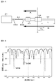
- FIG. 9A shows an outline of a system configuration used for verification of millimeter wave transmission by the millimeter wave cable 30.
- FIG. 9B shows frequency-amplitude characteristics when the termination condition of the millimeter wave cable 30 is switched to a condition of SHORT / OPEN.
- RBW resolution bandwidth
- a millimeter wave signal is generated and a reflected signal (reflected wave) reflected and returned at the end of the millimeter wave cable 30 is measured.
- a measuring device 61 is used.
- the millimeter wave signal generated by the signal generation / measurement device 61 is supplied to the millimeter wave cable 30 through the coaxial cable 62, the coaxial waveguide 63, and the waveguide adapter 64.
- One end of the coaxial cable 62 is connected to the input / output terminal of the signal generation / measurement device 61 via a connector (male / female) 65A, and the other end is connected to the coaxial waveguide 63 via a connector (male / female) 65B. It is connected.
- the joint surface (coupling surface) between the coaxial waveguide 63 and the waveguide adapter 64 becomes a reflection surface P due to impedance mismatch. Therefore, the millimeter wave signal supplied from the signal generating / measuring device 61 to the coaxial waveguide 63 through the coaxial cable 62 is reflected by the reflecting surface P, and the coaxial waveguide 63 and the coaxial cable are used as the A component of the reflected wave. Return to the signal generation / measurement device 61 through 62.
- the millimeter wave signal that has passed through the reflecting surface P is reflected at the end of the millimeter wave cable 30, and as a B component of the reflected wave, the millimeter wave cable 30, the waveguide adapter 64, the coaxial waveguide 63, and The signal is returned to the signal generation / measurement device 61 through the coaxial cable 62.
- the B component reflected at the end of the millimeter wave cable 30 is modulated by changing the termination condition of the millimeter wave cable 30, in this example, by switching SHORT / OPEN at the end of the millimeter wave cable 30.
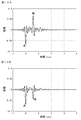
- FIG. 10A shows the time-amplitude characteristics when the end of the millimeter wave cable 30 is SHORT
- FIG. 10B shows the time-amplitude characteristics when the end of the millimeter wave cable 30 is OPEN.
- the phase of the B component is inverted by switching SHORT / OPEN at the end of the millimeter wave cable 30. Therefore, by placing information on the B component, it is possible to modulate the information into the millimeter wave band and transmit it using the millimeter wave cable 30.
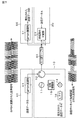
- termination condition variable section [Specific example of termination condition variable section] Next, a specific example of the termination condition variable unit 21 that changes the termination condition of the millimeter wave cable 30 used in the first to sixth embodiments will be described.
- FIG. 11A is a perspective view illustrating a coupling portion between the termination of the millimeter wave cable 30 and the termination condition variable unit 21,
- FIG. 11B is a plan view illustrating the coupling portion, and
- FIG. 11C illustrates the coupling portion. It is a side view including a partial cross section.
- the case where a waveguide 71 filled with a dielectric is used as the millimeter wave cable 30 is illustrated.
- the electromagnetic wave propagates through the dielectric while forming an electromagnetic field according to the wavelength (frequency) or the like.
- a notch 71A is formed at the end of the waveguide 71 filled with a dielectric that is the millimeter wave cable 30.
- the end of the printed circuit board 72 is fitted into the notch 71A.
- a CMOS chip 73 incorporating the termination condition variable unit 21 is mounted on the printed circuit board 72.
- An antenna pattern 74 is formed on the end surface of the printed circuit board 72. The antenna pattern 74 is electrically connected to the CMOS chip 73, and transmits signals by electromagnetic induction between the antenna pattern 74 and the waveguide 71 filled with a dielectric.
- a signal that is, a millimeter-wave reference signal
- a signal propagated through the waveguide 71 filled with a dielectric is transmitted to the CMOS chip 73 via the antenna pattern 74 on the printed circuit board 72.
- the termination condition variable unit 21 built in the CMOS chip 73, specifically, the CMOS chip 73 is terminated.
- FIG. 12 shows an example of the circuit configuration of the termination condition variable unit 21 including the termination structure of the millimeter wave cable 30.
- the termination condition variable unit 21 includes a switching transistor (FET) TR.
- the switching transistor TR has a source electrode grounded and a drain electrode connected to the power source V D via the inductor L.
- a balun BL is connected to the drain electrode of the switching transistor TR via a capacitor C.
- the antenna pattern 74 on the printed circuit board 72 outputs a millimeter-wave reference signal propagated through the waveguide 71 filled with a dielectric as a differential signal.
- This differential signal is converted into a single end by the balun BL, and is supplied to the drain electrode of the switching transistor TR via the capacitor C.
- the switching transistor TR by the gate voltage V G is modulated with transmission data, it modulates the reference signal of a millimeter wave applied through balun BL, and a capacitor C.
- the modulated millimeter-wave reference signal is supplied to the antenna pattern 74 via the capacitor C and the balun BL, and is transmitted to the waveguide 71 filled with a dielectric by electromagnetic induction.
- this indication can also take the following structures.
- a reference signal generation unit that generates a high-frequency reference signal and transmits the signal to a transmission circuit through a signal transmission path that transmits the radio wave while confining the radio wave in the transmission path;
- a transmission data restoring unit that receives the reference signal that is modulated based on the transmission data in the transmission circuit and is returned through the signal transmission path, and restores the transmission data;
- a receiving circuit A receiving circuit.
- the reception circuit according to [A01] further including a signal separation unit that separates a reference signal returned from the transmission circuit from a reference signal to be transmitted to the transmission circuit.
- [A03] The reception circuit according to [A02], wherein the signal separation unit temporally separates a reference signal transmitted to the transmission circuit and a reference signal returned from the transmission circuit.
- [A04] The reception circuit according to [A03], in which the reference signal generation unit transmits the next reference signal after receiving the reference signal returned from the transmission circuit.
- [A05] The reception circuit according to [A03], wherein the reference signal generation unit transmits the reference signal at a periodic interval that does not overlap with the reference signal returned from the transmission circuit.
- [A06] The reception circuit according to [A03], wherein the reference signal generation unit transmits the reference signal as a continuous signal to the transmission circuit.
- the transmission circuit receives the reference signal modulated by changing the termination condition of the signal transmission path based on the transmission data and returned through the signal transmission path.
- Receiver circuit receives the reference signal modulated by changing the termination condition of the signal transmission path based on the transmission data and returned through the signal transmission path.
- Receiver circuit receives the reference signal modulated by changing the termination condition of the signal transmission path based on the transmission data and returned through the signal transmission path.
- Receiver circuit receives the reference signal modulated by changing the termination condition of the signal transmission path based on the transmission data and returned through the signal transmission path.
- Receiver circuit receives the reference signal modulated by changing the termination condition of the signal transmission path based on the transmission data and returned through the signal transmission path.
- Receiver circuit receives the reference signal modulated by changing the termination condition of the signal transmission path based on the transmission data and returned through the signal transmission path.
- Receiver circuit receives the reference signal modulated by changing the termination condition of the signal transmission path based on the transmission data and returned through the signal transmission path.
- Transmission circuit A modulation unit that modulates a high-frequency reference signal transmitted from a receiving circuit through a signal transmission path that transmits the radio wave while confining the radio wave in the transmission path, and returns the modulated signal to the receiving circuit through the signal transmission path, A transmission circuit.
- the transmission circuit according to [B01] wherein the reference signal transmitted from the reception circuit through the signal transmission path is modulated based on the transmission data restored by the reception circuit, and is transmitted to the reception circuit through the signal transmission path.
- the modulation unit modulates the reference signal by changing a termination condition of the signal transmission path based on transmission data.
- [B04] The transmission circuit according to any one of [B01] to [B03], wherein the high-frequency reference signal is a millimeter-wave band signal.
- the high-frequency reference signal is a millimeter-wave band signal.
- the signal transmission path includes a waveguide or a waveguide.
- Communication system A transmission circuit for transmitting transmission data; A receiving circuit for generating a high-frequency reference signal; A signal transmission path for transmitting radio waves while confining radio waves in the transmission path between the transmission circuit and the reception circuit; With The transmission circuit modulates the reference signal transmitted from the reception circuit through the signal transmission path based on the transmission data, and returns to the reception circuit through the signal transmission path.
- the reception circuit is a communication system that receives a reference signal returned from a transmission circuit through a signal transmission path and restores transmission data.
- the transmission circuit A modulation unit that modulates a high-frequency reference signal transmitted from a receiving circuit through a signal transmission path based on transmission data;
- the signal transmission path includes a waveguide or a waveguide.
- [C06] The communication system according to any one of [C01] to [C05], wherein the signal transmission path has a fixed length.
- the receiving circuit A reference signal generator that generates a high-frequency reference signal and transmits the signal to a transmission circuit through a signal transmission path; A reference signal returned from the transmission circuit through the signal transmission path, and a transmission data restoration unit for restoring transmission data;
- the communication system according to any one of [C01] to [C06].
- [C08] The communication system according to any one of [C01] to [C07], wherein the reception circuit includes a signal separation unit that separates the reference signal returned from the transmission circuit from the reference signal transmitted to the transmission circuit.
- [C09] The communication system according to [C08], wherein the signal separation unit temporally separates the reference signal transmitted to the transmission circuit and the reference signal returned from the transmission circuit.
- [C10] The communication system according to [C09], in which the reference signal generation unit transmits the next reference signal after receiving the reference signal returned from the transmission circuit.
- [C11] The communication system according to [C09], in which the reference signal generation unit transmits the reference signal at a periodic interval that does not overlap with the reference signal returned from the transmission circuit.
- [C12] The communication system according to [C09], in which the reference signal generation unit transmits the reference signal as a continuous signal to the transmission circuit.
- the high-frequency reference signal generated in the receiving circuit is transmitted to the transmitting circuit through the signal transmission path that transmits the radio wave while confining the radio wave in the transmission path.
- a reference signal transmitted from the receiving circuit through the signal transmission path is modulated based on transmission data, and returned to the receiving circuit through the signal transmission path.
- the transmission circuit A modulation unit that modulates a high-frequency reference signal transmitted from the reception circuit through the signal transmission path based on the transmission data generated by the transmission data generation unit;
- the signal transmission path includes a waveguide or a waveguide.
- [D06] The communication method according to any one of [D01] to [D05], wherein the signal transmission path has a fixed length.
- the receiving circuit A reference signal generator that generates a high-frequency reference signal and transmits the signal to a transmission circuit through a signal transmission path; A reference signal returned from the transmission circuit through the signal transmission path, and a transmission data restoration unit for restoring transmission data;
- the communication method according to any one of [D01] to [D06], including: [D08] The communication method according to any one of [D01] to [D07], wherein the reception circuit includes a signal separation unit that separates a reference signal returned from the transmission circuit from a reference signal transmitted to the transmission circuit.
- [D09] The communication method according to [D08], in which the signal separation unit temporally separates the reference signal transmitted to the transmission circuit and the reference signal returned from the transmission circuit.
- [D10] The communication method according to [D09], in which the reference signal generation unit transmits the next reference signal after receiving the reference signal returned from the transmission circuit.
- [D11] The communication method according to [D09], in which the reference signal generation unit transmits the reference signal at a periodic interval that does not overlap with the reference signal returned from the transmission circuit.
- [D12] The communication method according to [D09], in which the reference signal generation unit transmits the reference signal as a continuous signal to the transmission circuit.
- SYMBOLS 1 Communication system, 10 ... Receiving circuit (load modulation receiving circuit), 11 ... Millimeter wave reference signal generation part, 12 ... Signal separation part, 13 ... Reflection signal extraction part, 14 * ..Multiplier, 15... Phase adjustment unit, 16... LPF (low pass filter), 17... Differential extraction unit, 20... Transmission circuit (load modulation transmission circuit), 21. Variable unit, 30 ... signal transmission path (millimeter wave cable), 40 ... millimeter wave transmission circuit, 41 ... BPSK modulation unit, 50 ... millimeter wave reception circuit, 51 ... BPSK demodulation unit, 52 ... detection unit, 53 ... reference signal clock recovery unit, 61 ... signal generation / measurement device, 62 ...
- coaxial cable 63 ... coaxial waveguide, 64 ... waveguide Adapter, 71 ... Waveguide filled with dielectric, 72 ... Printed circuit board 73 ... CMOS chip, 74 ... antenna pattern, 100 ... first communication device, 200 ... second communication device, BL ... balun, C ... capacitor, L ... Inductors
Priority Applications (4)
| Application Number | Priority Date | Filing Date | Title |
|---|---|---|---|
| EP14823158.2A EP3021493B1 (en) | 2013-07-09 | 2014-06-05 | Receiving circuit and transmitting circuit; communication system and communication method |
| CN201480037600.3A CN105359421A (zh) | 2013-07-09 | 2014-06-05 | 接收电路和发送电路、通信系统和通信方法 |
| US14/902,073 US10277274B2 (en) | 2013-07-09 | 2014-06-05 | Receiving circuit and transmitting circuit, and communication system and communication method |
| CN201911358147.7A CN110912583B (zh) | 2013-07-09 | 2014-06-05 | 接收电路和发送电路、通信系统和通信方法 |
Applications Claiming Priority (2)
| Application Number | Priority Date | Filing Date | Title |
|---|---|---|---|
| JP2013-143330 | 2013-07-09 | ||
| JP2013143330A JP2015019137A (ja) | 2013-07-09 | 2013-07-09 | 受信回路及び送信回路、並びに、通信システム及び通信方法 |
Publications (1)
| Publication Number | Publication Date |
|---|---|
| WO2015005032A1 true WO2015005032A1 (ja) | 2015-01-15 |
Family
ID=52279725
Family Applications (1)
| Application Number | Title | Priority Date | Filing Date |
|---|---|---|---|
| PCT/JP2014/064939 WO2015005032A1 (ja) | 2013-07-09 | 2014-06-05 | 受信回路及び送信回路、並びに、通信システム及び通信方法 |
Country Status (5)
| Country | Link |
|---|---|
| US (1) | US10277274B2 (zh) |
| EP (1) | EP3021493B1 (zh) |
| JP (1) | JP2015019137A (zh) |
| CN (2) | CN105359421A (zh) |
| WO (1) | WO2015005032A1 (zh) |
Families Citing this family (39)
| Publication number | Priority date | Publication date | Assignee | Title |
|---|---|---|---|---|
| US9973299B2 (en) | 2014-10-14 | 2018-05-15 | At&T Intellectual Property I, L.P. | Method and apparatus for adjusting a mode of communication in a communication network |
| US9312919B1 (en) | 2014-10-21 | 2016-04-12 | At&T Intellectual Property I, Lp | Transmission device with impairment compensation and methods for use therewith |
| US9653770B2 (en) * | 2014-10-21 | 2017-05-16 | At&T Intellectual Property I, L.P. | Guided wave coupler, coupling module and methods for use therewith |
| US9461706B1 (en) | 2015-07-31 | 2016-10-04 | At&T Intellectual Property I, Lp | Method and apparatus for exchanging communication signals |
| US10009067B2 (en) | 2014-12-04 | 2018-06-26 | At&T Intellectual Property I, L.P. | Method and apparatus for configuring a communication interface |
| US9954287B2 (en) | 2014-11-20 | 2018-04-24 | At&T Intellectual Property I, L.P. | Apparatus for converting wireless signals and electromagnetic waves and methods thereof |
| US9997819B2 (en) | 2015-06-09 | 2018-06-12 | At&T Intellectual Property I, L.P. | Transmission medium and method for facilitating propagation of electromagnetic waves via a core |
| US10243784B2 (en) | 2014-11-20 | 2019-03-26 | At&T Intellectual Property I, L.P. | System for generating topology information and methods thereof |
| US9876570B2 (en) | 2015-02-20 | 2018-01-23 | At&T Intellectual Property I, Lp | Guided-wave transmission device with non-fundamental mode propagation and methods for use therewith |
| US9490869B1 (en) | 2015-05-14 | 2016-11-08 | At&T Intellectual Property I, L.P. | Transmission medium having multiple cores and methods for use therewith |
| US9871282B2 (en) | 2015-05-14 | 2018-01-16 | At&T Intellectual Property I, L.P. | At least one transmission medium having a dielectric surface that is covered at least in part by a second dielectric |
| US10650940B2 (en) | 2015-05-15 | 2020-05-12 | At&T Intellectual Property I, L.P. | Transmission medium having a conductive material and methods for use therewith |
| US9866309B2 (en) | 2015-06-03 | 2018-01-09 | At&T Intellectual Property I, Lp | Host node device and methods for use therewith |
| US9912381B2 (en) | 2015-06-03 | 2018-03-06 | At&T Intellectual Property I, Lp | Network termination and methods for use therewith |
| US9913139B2 (en) | 2015-06-09 | 2018-03-06 | At&T Intellectual Property I, L.P. | Signal fingerprinting for authentication of communicating devices |
| US9820146B2 (en) | 2015-06-12 | 2017-11-14 | At&T Intellectual Property I, L.P. | Method and apparatus for authentication and identity management of communicating devices |
| US9865911B2 (en) | 2015-06-25 | 2018-01-09 | At&T Intellectual Property I, L.P. | Waveguide system for slot radiating first electromagnetic waves that are combined into a non-fundamental wave mode second electromagnetic wave on a transmission medium |
| US9640850B2 (en) | 2015-06-25 | 2017-05-02 | At&T Intellectual Property I, L.P. | Methods and apparatus for inducing a non-fundamental wave mode on a transmission medium |
| US9847566B2 (en) | 2015-07-14 | 2017-12-19 | At&T Intellectual Property I, L.P. | Method and apparatus for adjusting a field of a signal to mitigate interference |
| US9853342B2 (en) | 2015-07-14 | 2017-12-26 | At&T Intellectual Property I, L.P. | Dielectric transmission medium connector and methods for use therewith |
| US10044409B2 (en) | 2015-07-14 | 2018-08-07 | At&T Intellectual Property I, L.P. | Transmission medium and methods for use therewith |
| US9871283B2 (en) | 2015-07-23 | 2018-01-16 | At&T Intellectual Property I, Lp | Transmission medium having a dielectric core comprised of plural members connected by a ball and socket configuration |
| US9749053B2 (en) | 2015-07-23 | 2017-08-29 | At&T Intellectual Property I, L.P. | Node device, repeater and methods for use therewith |
| US9912027B2 (en) | 2015-07-23 | 2018-03-06 | At&T Intellectual Property I, L.P. | Method and apparatus for exchanging communication signals |
| US9948333B2 (en) | 2015-07-23 | 2018-04-17 | At&T Intellectual Property I, L.P. | Method and apparatus for wireless communications to mitigate interference |
| US9967173B2 (en) | 2015-07-31 | 2018-05-08 | At&T Intellectual Property I, L.P. | Method and apparatus for authentication and identity management of communicating devices |
| US9904535B2 (en) | 2015-09-14 | 2018-02-27 | At&T Intellectual Property I, L.P. | Method and apparatus for distributing software |
| US9876264B2 (en) | 2015-10-02 | 2018-01-23 | At&T Intellectual Property I, Lp | Communication system, guided wave switch and methods for use therewith |
| US9860075B1 (en) | 2016-08-26 | 2018-01-02 | At&T Intellectual Property I, L.P. | Method and communication node for broadband distribution |
| US10811767B2 (en) | 2016-10-21 | 2020-10-20 | At&T Intellectual Property I, L.P. | System and dielectric antenna with convex dielectric radome |
| US10312567B2 (en) | 2016-10-26 | 2019-06-04 | At&T Intellectual Property I, L.P. | Launcher with planar strip antenna and methods for use therewith |
| US10225025B2 (en) | 2016-11-03 | 2019-03-05 | At&T Intellectual Property I, L.P. | Method and apparatus for detecting a fault in a communication system |
| US10178445B2 (en) | 2016-11-23 | 2019-01-08 | At&T Intellectual Property I, L.P. | Methods, devices, and systems for load balancing between a plurality of waveguides |
| US10637149B2 (en) | 2016-12-06 | 2020-04-28 | At&T Intellectual Property I, L.P. | Injection molded dielectric antenna and methods for use therewith |
| US9998870B1 (en) | 2016-12-08 | 2018-06-12 | At&T Intellectual Property I, L.P. | Method and apparatus for proximity sensing |
| US10389037B2 (en) | 2016-12-08 | 2019-08-20 | At&T Intellectual Property I, L.P. | Apparatus and methods for selecting sections of an antenna array and use therewith |
| US9838896B1 (en) | 2016-12-09 | 2017-12-05 | At&T Intellectual Property I, L.P. | Method and apparatus for assessing network coverage |
| JP7344650B2 (ja) * | 2019-02-25 | 2023-09-14 | オリンパス株式会社 | 撮像装置、撮像装置を含む内視鏡装置、および撮像装置を含む移動体 |
| KR102421478B1 (ko) * | 2021-01-20 | 2022-07-14 | 연세대학교 산학협력단 | 변조 방법, 복조 방법 및 이들을 이용하는 변조 장치 및 복조 장치 |
Citations (2)
| Publication number | Priority date | Publication date | Assignee | Title |
|---|---|---|---|---|
| JP2005101892A (ja) * | 2003-09-25 | 2005-04-14 | Sony Corp | 通信システム、通信装置および通信方法、記録媒体、並びにプログラム |
| EP2199947A1 (en) * | 2008-12-17 | 2010-06-23 | Legic Identsystems Ag | Device for reading data from a transponder module |
Family Cites Families (18)
| Publication number | Priority date | Publication date | Assignee | Title |
|---|---|---|---|---|
| WO1992017866A1 (en) * | 1991-04-03 | 1992-10-15 | Integrated Silicon Design Pty. Ltd. | Article sorting system |
| JP2003526990A (ja) * | 2000-03-01 | 2003-09-09 | ヴァヴィク、ゲイル・モンセン | トランスポンダおよびトランスポンダシステム |
| US6525545B2 (en) * | 2001-02-28 | 2003-02-25 | Tektronix, Inc. | Frequency domain reflection measurement device |
| US7164274B2 (en) * | 2003-06-11 | 2007-01-16 | Broadcom Corporation | Cable diagnostics using time domain reflectometry and applications using the same |
| JP4446785B2 (ja) * | 2003-08-27 | 2010-04-07 | 京セラ株式会社 | 高周波送受信器およびそれを具備するレーダ装置ならびにそれを搭載したレーダ装置搭載車両およびレーダ装置搭載小型船舶 |
| US7627025B2 (en) * | 2004-07-01 | 2009-12-01 | Broadcom Corporation | Echo canceller gain control for channel diagnostic systems |
| US20080030305A1 (en) * | 2006-05-16 | 2008-02-07 | O'connor Ruaidhri M | Systems and Methods for Using a Tag |
| JP2008123231A (ja) * | 2006-11-10 | 2008-05-29 | Hitachi Ltd | Rfidタグ読取システムおよびrfidタグ読取方法 |
| US8121541B2 (en) * | 2007-01-31 | 2012-02-21 | Broadcom Corporation | Integrated circuit with intra-chip and extra-chip RF communication |
| US7808247B1 (en) * | 2007-02-22 | 2010-10-05 | Marvel International Ltd. | Fast cable tester |
| JP2010103982A (ja) * | 2008-09-25 | 2010-05-06 | Sony Corp | ミリ波伝送装置、ミリ波伝送方法、ミリ波伝送システム |
| US8410786B1 (en) * | 2008-10-06 | 2013-04-02 | Anritsu Company | Passive intermodulation (PIM) distance to fault analyzer with selectable harmonic level |
| JP2010160978A (ja) * | 2009-01-08 | 2010-07-22 | Sony Corp | 高周波信号伝送システム、高周波信号伝送コネクタおよび高周波信号伝送ケーブル |
| JP4752932B2 (ja) * | 2009-02-25 | 2011-08-17 | 株式会社デンソー | 送信装置、受信装置、及び送受信装置 |
| JP5278210B2 (ja) * | 2009-07-13 | 2013-09-04 | ソニー株式会社 | 無線伝送システム、電子機器 |
| US20110053536A1 (en) * | 2009-09-03 | 2011-03-03 | Provigent Ltd | Receiver with re-demodulation |
| US8582443B1 (en) * | 2009-11-23 | 2013-11-12 | Marvell International Ltd. | Method and apparatus for virtual cable test using echo canceller coefficients |
| WO2014058432A1 (en) * | 2012-10-12 | 2014-04-17 | Nokia Siemens Networks Oy | Vswr estimation using correlation to suppress external interference |
-
2013
- 2013-07-09 JP JP2013143330A patent/JP2015019137A/ja active Pending
-
2014
- 2014-06-05 US US14/902,073 patent/US10277274B2/en active Active
- 2014-06-05 WO PCT/JP2014/064939 patent/WO2015005032A1/ja active Application Filing
- 2014-06-05 CN CN201480037600.3A patent/CN105359421A/zh active Pending
- 2014-06-05 CN CN201911358147.7A patent/CN110912583B/zh active Active
- 2014-06-05 EP EP14823158.2A patent/EP3021493B1/en not_active Not-in-force
Patent Citations (2)
| Publication number | Priority date | Publication date | Assignee | Title |
|---|---|---|---|---|
| JP2005101892A (ja) * | 2003-09-25 | 2005-04-14 | Sony Corp | 通信システム、通信装置および通信方法、記録媒体、並びにプログラム |
| EP2199947A1 (en) * | 2008-12-17 | 2010-06-23 | Legic Identsystems Ag | Device for reading data from a transponder module |
Non-Patent Citations (3)
| Title |
|---|
| P. PURSULA: "60-GHz Millimeter-Wave Identification Reader on 90-nm CMOS and LTCC", IEEE TRANSACTIONS ON MICROWAVE THEORY AND TECHNIQUES, vol. 59, no. 4, April 2011 (2011-04-01), XP011372553, DOI: doi:10.1109/TMTT.2011.2114200 |
| P. PURSULA: "Millimeter-Wave Identification-A New Short Radio System for Low-Power High Data-Rate Application", IEEE TRANSACTIONS ON MICROWAVE THEORY AND TECHNIQUES, vol. 56, no. 10, October 2008 (2008-10-01), XP011235159, DOI: doi:10.1109/TMTT.2008.2004252 |
| See also references of EP3021493A4 |
Also Published As
| Publication number | Publication date |
|---|---|
| CN110912583B (zh) | 2022-06-10 |
| CN105359421A (zh) | 2016-02-24 |
| US20160373164A1 (en) | 2016-12-22 |
| JP2015019137A (ja) | 2015-01-29 |
| EP3021493A1 (en) | 2016-05-18 |
| US10277274B2 (en) | 2019-04-30 |
| EP3021493B1 (en) | 2018-03-21 |
| EP3021493A4 (en) | 2017-02-22 |
| CN110912583A (zh) | 2020-03-24 |
Similar Documents
| Publication | Publication Date | Title |
|---|---|---|
| WO2015005032A1 (ja) | 受信回路及び送信回路、並びに、通信システム及び通信方法 | |
| US10447514B2 (en) | Wireless transmission system, wireless communication device, and wireless communication method | |
| RU2517059C2 (ru) | Устройство беспроводной связи, система беспроводной передачи данных и способ беспроводной передачи данных | |
| US8824529B2 (en) | Signal transmission system, transmitting device, receiving device, electronic device, and signal transmission method | |
| JP6381522B2 (ja) | コネクタ装置及び無線伝送システム | |
| US8947180B2 (en) | Signal transmission device, electronic device, and signal transmission method | |
| US8736396B2 (en) | Radio communicating device, rotational structure, and electronic device | |
| US7696835B2 (en) | Communication system, transmitting device, transmitting method, receiving device, and receiving method | |
| US20120195348A1 (en) | Signal transmission apparatus, electronic instrument, reference signal outputting apparatus, communication apparatus, reference signal reception apparatus and signal transmission method | |
| WO2014174983A1 (ja) | コネクタ装置及び無線伝送システム | |
| US10205620B2 (en) | Transmission circuit, transmission method, and transmission system | |
| JP5725222B2 (ja) | 無線伝送システム、無線通信装置、無線通信方法 | |
| WO2014174991A1 (ja) | コネクタ装置及び無線伝送システム | |
| Saponara | Integrated Circuits & Systems for mm-wave/RF Wireless Transceivers in IoT Applications (Communications) | |
| JP2011055094A (ja) | 無線伝送システム、無線通信装置、無線通信方法 | |
| WO2018140962A1 (en) | Millimeter-wave cmos transceiver with pcb antenna for contactless wave-connectors |
Legal Events
| Date | Code | Title | Description |
|---|---|---|---|
| WWE | Wipo information: entry into national phase |
Ref document number: 201480037600.3 Country of ref document: CN |
|
| 121 | Ep: the epo has been informed by wipo that ep was designated in this application |
Ref document number: 14823158 Country of ref document: EP Kind code of ref document: A1 |
|
| WWE | Wipo information: entry into national phase |
Ref document number: 2014823158 Country of ref document: EP |
|
| WWE | Wipo information: entry into national phase |
Ref document number: 14902073 Country of ref document: US |
|
| NENP | Non-entry into the national phase |
Ref country code: DE |