WO2014208339A1 - 電圧発生回路 - Google Patents
電圧発生回路 Download PDFInfo
- Publication number
- WO2014208339A1 WO2014208339A1 PCT/JP2014/065491 JP2014065491W WO2014208339A1 WO 2014208339 A1 WO2014208339 A1 WO 2014208339A1 JP 2014065491 W JP2014065491 W JP 2014065491W WO 2014208339 A1 WO2014208339 A1 WO 2014208339A1
- Authority
- WO
- WIPO (PCT)
- Prior art keywords
- terminal
- voltage
- transistor
- power supply
- circuit
- Prior art date
- Legal status (The legal status is an assumption and is not a legal conclusion. Google has not performed a legal analysis and makes no representation as to the accuracy of the status listed.)
- Ceased
Links
Images











Classifications
-
- G—PHYSICS
- G05—CONTROLLING; REGULATING
- G05F—SYSTEMS FOR REGULATING ELECTRIC OR MAGNETIC VARIABLES
- G05F3/00—Non-retroactive systems for regulating electric variables by using an uncontrolled element, or an uncontrolled combination of elements, such element or such combination having self-regulating properties
- G05F3/02—Regulating voltage or current
- G05F3/08—Regulating voltage or current wherein the variable is DC
- G05F3/10—Regulating voltage or current wherein the variable is DC using uncontrolled devices with non-linear characteristics
- G05F3/16—Regulating voltage or current wherein the variable is DC using uncontrolled devices with non-linear characteristics being semiconductor devices
- G05F3/20—Regulating voltage or current wherein the variable is DC using uncontrolled devices with non-linear characteristics being semiconductor devices using diode- transistor combinations
- G05F3/22—Regulating voltage or current wherein the variable is DC using uncontrolled devices with non-linear characteristics being semiconductor devices using diode- transistor combinations wherein the transistors are of the bipolar type only
- G05F3/222—Regulating voltage or current wherein the variable is DC using uncontrolled devices with non-linear characteristics being semiconductor devices using diode- transistor combinations wherein the transistors are of the bipolar type only with compensation for device parameters, e.g. Early effect, gain, manufacturing process, or external variations, e.g. temperature, loading, supply voltage
- G05F3/227—Regulating voltage or current wherein the variable is DC using uncontrolled devices with non-linear characteristics being semiconductor devices using diode- transistor combinations wherein the transistors are of the bipolar type only with compensation for device parameters, e.g. Early effect, gain, manufacturing process, or external variations, e.g. temperature, loading, supply voltage producing a current or voltage as a predetermined function of the supply voltage
-
- G—PHYSICS
- G05—CONTROLLING; REGULATING
- G05F—SYSTEMS FOR REGULATING ELECTRIC OR MAGNETIC VARIABLES
- G05F1/00—Automatic systems in which deviations of an electric quantity from one or more predetermined values are detected at the output of the system and fed back to a device within the system to restore the detected quantity to its predetermined value or values, i.e. retroactive systems
- G05F1/10—Regulating voltage or current
- G05F1/46—Regulating voltage or current wherein the variable actually regulated by the final control device is DC
- G05F1/56—Regulating voltage or current wherein the variable actually regulated by the final control device is DC using semiconductor devices in series with the load as final control devices
-
- G—PHYSICS
- G05—CONTROLLING; REGULATING
- G05F—SYSTEMS FOR REGULATING ELECTRIC OR MAGNETIC VARIABLES
- G05F3/00—Non-retroactive systems for regulating electric variables by using an uncontrolled element, or an uncontrolled combination of elements, such element or such combination having self-regulating properties
- G05F3/02—Regulating voltage or current
- G05F3/08—Regulating voltage or current wherein the variable is DC
- G05F3/10—Regulating voltage or current wherein the variable is DC using uncontrolled devices with non-linear characteristics
- G05F3/16—Regulating voltage or current wherein the variable is DC using uncontrolled devices with non-linear characteristics being semiconductor devices
- G05F3/20—Regulating voltage or current wherein the variable is DC using uncontrolled devices with non-linear characteristics being semiconductor devices using diode- transistor combinations
- G05F3/22—Regulating voltage or current wherein the variable is DC using uncontrolled devices with non-linear characteristics being semiconductor devices using diode- transistor combinations wherein the transistors are of the bipolar type only
Definitions
- the present invention relates to a voltage generation circuit having a small power supply voltage dependency.
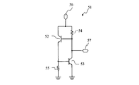
- FIG. 18 is a circuit diagram of an example of a conventional voltage generating circuit.
- the voltage generation circuit 51 is a circuit in which transistors 52 and 53 and resistors 54 and 55 are connected.
- the sum of the base-emitter voltages (Vbe) of the transistors 52 and 53, that is, an output voltage twice as large as Vbe is output to the voltage output terminal 57.
- This voltage generation circuit 51 has the property that “the voltage generated at the voltage output terminal increases as the power supply voltage increases”, and the dependence of the output voltage on the power supply voltage is not small.
- FIG. 19 is a circuit diagram of another example of a conventional voltage generating circuit.
- a voltage generation circuit 61 shown in FIG. 19 is obtained by adding a resistor 62 between the base terminal of the transistor 52 of the voltage generation circuit 51 and the voltage output terminal 57.
- the rest of the configuration is the same as that of the voltage generation circuit 51, and substantially the same elements and terminals are denoted by the same numbers.
- the voltage generation circuit 61 In the voltage generation circuit 61, an effect of “lowering the voltage generated at the voltage output terminal in accordance with the increase of the power supply voltage” is generated by the action of the voltage drop of the resistor 62, and the “power supply voltage becomes higher” of the voltage generation circuit 51. Therefore, a part of the property that the voltage generated at the voltage output terminal becomes high is canceled out. Due to the effect of the resistor 62, the dependency of the output voltage on the power supply voltage can be reduced. Alternatively, the characteristics can be adjusted so that the output voltage becomes a maximum value at a certain power supply voltage and the output voltage starts decreasing at a power supply voltage higher than that. That is, the voltage generation circuit 61 is a circuit in which the power supply voltage dependency of the output voltage is reduced with respect to the voltage generation circuit 51. In particular, the voltage generation circuit 61 becomes an excellent circuit that can be used as a voltage generation circuit with very little power supply voltage dependency by using it near the power supply voltage at which the output voltage becomes a maximum value.
- FIG. 20 is a diagram showing the relationship between the output voltage of the voltage generation circuit shown in FIGS. 18 and 19 and the power supply voltage.
- a graph curve 71 is a graph showing the relationship between the output voltage (vertical axis) of the voltage generation circuit 51 and the power supply voltage (horizontal axis)
- a graph curve 72 is the output voltage (vertical axis) of the voltage generation circuit 61. It is a graph which shows the relationship of a power supply voltage (horizontal axis), and each calculates the output voltage of the voltage generation circuits 51 and 61 by circuit simulation.
- each resistor was 3200 ⁇ for the resistor 54, 8000 ⁇ for the resistor 55, and 50 ⁇ for the resistor 62 (only the voltage generation circuit 61).
- the transistors 52 and 53 are GaAs heterojunction bipolar transistors with an emitter size of 48 ⁇ m 2 .
- the output voltage (graph curve 71) of the voltage generation circuit 51 gradually increases as the power supply voltage increases. That is, it can be seen that the voltage generation circuit 51 is a circuit in which the output voltage is highly dependent on the power supply voltage.
- the output voltage (graph curve 72) of the voltage generation circuit 61 increases as the power supply voltage increases, but reaches a local maximum when the power supply voltage reaches about 4V, and then decreases as the power supply voltage increases. ing. That is, the voltage generation circuit 61 can be used as a voltage generation circuit that has very little power supply voltage dependency when used with a power supply voltage in the vicinity of 4V.
- the voltage generation circuit 61 shown in FIG. 19 can change the power supply voltage at the peak of the output voltage by changing the resistance value of the resistor 62.
- a graph curve 73 is a graph showing the relationship between the output voltage and the power supply voltage when the resistance 62 of the voltage generation circuit 61 is changed to 100 ⁇
- the graph curve 74 is a resistance 62 of the voltage generation circuit 61 set to 150 ⁇ . It is a graph which shows the relationship between the output voltage and power supply voltage at the time.
- the power supply voltage at which the output voltage becomes the maximum value moves to the low voltage side.
- the power supply voltage range with less power supply voltage dependency can be adjusted to the low voltage side.
- the “power supply voltage at which the output voltage reaches the maximum value moves to the low voltage side” the “power supply voltage range with less power supply voltage dependency” of the output voltage becomes narrower, and the output at which the output voltage reaches the maximum value. The voltage value has dropped.
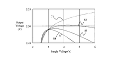
- FIG. 21 is a diagram showing the relationship between the output voltage and the power supply voltage when the resistance and transistor of the voltage generation circuit shown in FIGS. 18 and 19 are changed.
- the output voltage when the power supply voltage is 3 V is adjusted by changing the element size of the transistor 52 of the voltage generation circuit 61 so that the output voltage becomes the same as the output voltage (graph curve 71) of the voltage generation circuit 51. Shows the output voltage.
- the results of adjusting the size of the transistor 52 to 0.74 times, 0.53 times, and 0.4 times the original size, respectively, are graph curves 82, 83, 84.
- the output voltage does not change until the power supply voltage is as low as possible so that fluctuations in the output voltage are reduced even when the power supply voltage drops due to battery consumption.
- the power supply voltage dependency on the side is greatly deteriorated.
- the output voltage can be increased by reducing the resistance 54 and the resistance 55, it is still possible to suppress the deterioration at a high power supply voltage while improving the power supply voltage dependency at a low power supply voltage. difficult.
- an object of the present invention is to provide a voltage generation circuit which has a simple configuration, improves power supply voltage dependency when the power supply voltage is low, and has low power supply voltage dependency in a wide power supply voltage range. To do.
- the present invention provides a first power supply terminal, a voltage output terminal, a first resistor, a first bipolar transistor, a second bipolar transistor, a first circuit, and a second circuit.
- a first terminal of the first resistor is connected to the first power supply terminal, an emitter terminal of the first bipolar transistor is connected to a ground terminal, A first terminal of the first circuit is connected to a second terminal of the first resistor, and a second terminal of the first circuit is connected to a collector terminal of the first bipolar transistor.
- the first circuit has a diode and a resistor, and the forward direction of the diode junction is between the first terminal of the first circuit and the second terminal of the first circuit.
- the sum of the junction voltage and the voltage drop due to the resistance is A circuit to be generated according to the current, or a bipolar transistor and a resistor, and a base-emitter junction is provided between the first terminal of the first circuit and the second terminal of the first circuit.
- a second terminal of the second circuit is connected to a base terminal of the first bipolar transistor, the second circuit includes a diode, and the second terminal A circuit for generating a forward junction voltage of a diode junction in response to a diode current, or a bipolar transistor, between a first terminal of the circuit and a second terminal of the second circuit, A first terminal of the second circuit; A circuit that generates a forward junction voltage of a base-emitter junction according to an emitter current between the second terminal of the second circuit and the emitter terminal of the second bipolar transistor; Is connected to the ground terminal, the collector terminal of the second bipolar transistor is connected to the base terminal of the first bipolar transistor, and the base terminal of the second bipolar transistor is the second terminal of the first circuit.
- the base emitter junction of the first bipolar transistor and the base emitter junction of the second bipolar transistor are connected in the forward direction with respect to the potential of the first power supply terminal, and the voltage output Voltage generation characterized in that the terminal is connected directly or via a resistor to the second terminal of the first resistor Provide a circuit.
- the present invention it is possible to provide a voltage generation circuit having a simple configuration, improving the power supply voltage dependency when the power supply voltage is low, and having a low power supply voltage dependency in a wide power supply voltage range.
- FIG. 11B is a circuit diagram which shows the other example of the voltage generation circuit concerning this invention.
- FIG. 13B is a circuit diagram showing a replaceable circuit of the voltage generating circuit shown in FIG. 13A. It is a figure which shows the relationship between the output voltage of the voltage generation circuit concerning this invention, and a power supply voltage. It is a figure which shows the other example of the voltage generation circuit concerning this invention. It is a figure which shows the relationship between the output voltage of the voltage generation circuit concerning this invention, and a power supply voltage. It is a figure which shows the relationship of the power supply voltage of the output voltage of the voltage generation circuit shown in FIG. It is a figure which shows an example of the high frequency power amplifier circuit using the voltage generation circuit concerning this invention.
- FIG. 20 is a diagram illustrating a relationship between an output voltage of the voltage generation circuit illustrated in FIGS. 18 and 19 and a power supply voltage.
- FIG. 20 is a diagram illustrating a relationship between an output voltage and a power supply voltage when resistances and transistors of the voltage generation circuit illustrated in FIGS. 18 and 19 are changed.
- the power supply voltage applied to the power supply terminal is set to a positive value, and an example of a circuit configuration using an NPN bipolar transistor is described.
- the present invention is not limited to this.
- the same effect can be obtained by using a PNP bipolar transistor with the same circuit configuration and making the power supply voltage and output voltage negative.
- the voltage and current values in the following explanation are compared as absolute voltage values and current value comparisons, and the diode electrode is connected to the anode terminal and the cathode terminal. It shall be read in reverse.
- the same numbers are used for parts and terminals having the same configuration, and even in the diagrams showing the characteristics, simulation is performed using the same element values for parts having the same symbols unless otherwise specified.
- the calculated result is shown.
- a GaAs heterojunction bipolar transistor having an emitter area of 48 ⁇ m 2 is used as the transistor.
- the emitter area is expressed as a ratio to the above size (48 ⁇ m 2 ).
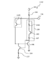
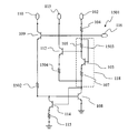
- FIG. 1 is a circuit diagram showing a configuration of an example of a voltage generation circuit according to the present embodiment.
- the power supply terminal 102 and the base terminal of the transistor 103 are connected by a resistor 104.
- the base terminal of the transistor 103 is connected to the collector terminal of the transistor 103 via the resistors 105 and 106, and the emitter terminal of the transistor 103 is connected to the collector terminal of the transistor 108 via the resistor 107.
- the emitter terminal of the transistor 108 is grounded, and the base terminal of the transistor 108 is connected to the emitter terminal of the transistor 109. Further, the base terminal of the transistor 109 is connected to the power supply terminal 102 via the resistor 104, the collector terminal of the transistor 109 is connected to the power supply terminal 110, and the emitter terminal of the transistor 109 is connected to the ground terminal via the resistor 111. Yes.
- the base terminal of the transistor 112 is connected to the collector terminal of the transistor 103, the emitter terminal of the transistor 112 is connected to the emitter terminal of the transistor 103, and the collector terminal of the transistor 112 is connected to the power supply terminal 113.
- the base terminal of the transistor 114 is connected to the collector terminal of the transistor 108, the collector terminal of the transistor 114 is connected to the base terminal of the transistor 108, and the emitter terminal of the transistor 114 is grounded through the resistor 115.
- a terminal 116 connected to the base terminal of the transistor 109 or a terminal 117 connected between the resistors 105 and 106 is used as a power output terminal.
- the power terminal 102 is a first power terminal
- the power terminals 113 and 110 are power terminals having the same polarity as the first power terminal.
- the resistor 104 is a first resistor
- the transistor 108 is a first bipolar transistor
- a transistor 103 and a resistor 107 in which the base collector is connected by resistors 105 and 106 and a resistor 107 are a first circuit indicated by a broken line.
- 118 is constituted.
- the first circuit 118 includes a forward junction voltage of the base-emitter junction of the transistor 103 between the first terminal connected to the terminal 116 and the second terminal connected to the collector terminal of the transistor 108.
- the sum of the voltage drop of the resistor 107 is generated in accordance with the emitter current of the transistor 103.
- the transistor 109 is a second circuit, and includes a first terminal connected to the terminal 116 (a first terminal of the first circuit) and a second terminal connected to the base terminal of the transistor 108. In the meantime, the forward junction voltage of the base emitter junction is generated according to the emitter current.
- the transistor 114 is a second bipolar transistor, the transistor 103 is a third bipolar transistor, and the transistor 112 is a fourth bipolar transistor.
- the path from the base terminal of the transistor 103 to the collector terminal of the transistor 103 via the resistors 105 and 106 is the first connection path.
- the connection point between the base terminal of the transistor 103 and the resistor 105 is a first connection terminal on the first connection path.
- the emitter terminal of the transistor 112 is connected to the path from the emitter terminal of the transistor 103 to the collector terminal of the transistor 108 via the resistor 107.
- the emitter terminal of the transistor 112 is connected to the emitter terminal of the transistor 103.
- the base terminal of the transistor 112 is connected to a first path between the first connection terminal and the collector terminal of the transistor 103, and resistors 105 and 106 are connected between the base terminal of the transistor 112 and the first connection terminal. have.
- the resistor 104 is 3200 ⁇
- the resistor 105 is 45 ⁇
- the resistor 106 is 155 ⁇
- the resistor 107 is 200 ⁇
- the resistor 111 is 8000 ⁇
- the resistor 115 is 20 ⁇ .
- the power supply voltages 102, 110, and 113 are all set to the same potential.
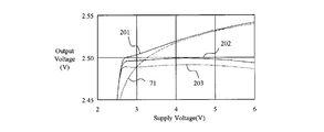
- FIG. 2 is a diagram showing the relationship between the output voltage and the power supply voltage of the voltage generating circuit according to the present invention.
- a graph curve 201 indicates the relationship between the output voltage of the voltage generation circuit 101 and the power supply voltage when the terminal 116 is used as a voltage output terminal
- the graph curve 202 indicates the voltage at the terminal 117.
- the relationship between the output voltage of the circuit 101 and the power supply voltage when used as an output terminal is shown.
- a graph curve 203 shows the relationship between the output voltage of the voltage generation circuit 101 and the power supply voltage when the resistance value of the resistor 111 is 11000 ⁇ . The resistance value of the resistor 111 is adjusted such that when the power supply voltage is 3 V, the output voltage at the terminal 117 is the same as that of the conventional voltage generation circuit 51.
- the graph of FIG. 2 shows a graph curve 71 showing the relationship between the output voltage of the conventional voltage generation circuit 51 and the power supply voltage.
- the output voltage of the conventional voltage generation circuit 51 increases with an increase in the power supply voltage while the slope becomes gentle. In other words, “When the power supply voltage decreases, the slope increases and the output voltage decreases.”
- the output voltage at the low power supply voltage when the terminal 116 of the voltage generation circuit 101 is the voltage output terminal is higher than the output voltage of the conventional voltage generation circuit 51 (graph curve 71). It has become. As a result, the characteristic that the slope increases and the output voltage decreases as the power supply voltage becomes lower is improved, and the slope when the power supply voltage is about 2.7 V or more approaches a straight line.
- the output voltage when the terminal 117 of the voltage generation circuit 101 is used as the voltage output terminal is approximately constant at a power supply voltage of about 2.7 V or higher.
- the voltage generation circuit according to the present invention aims to improve the power supply voltage dependency of the output voltage, and in particular, aims to improve by increasing the output voltage at a low power supply voltage. Therefore, if the output voltage is high, the output voltage at the low power supply voltage will be high, and it will appear to improve at first glance, or if the resistance 104 or the resistance 111 is reduced, the circuit current will increase greatly, and the circuit current will increase. It may appear to be improved compared to the low case. Therefore, when the comparison is performed, the resistor 104 as the first resistor is set to 3200 ⁇ , which is the same as the resistor 54 of the conventional voltage generation circuit 51, and the resistor 111 does not become smaller than 8000 ⁇ of the resistor 55 of the circuit 51 of the prior art. The characteristics are compared by setting to.
- the characteristic is confirmed by also showing a graph of the result of adjusting the element value so that the output voltage is the same as that of the comparison circuit at the power supply voltage of 3V.
- the voltage generation circuit 101 in which the value of the resistor 111 is changed As compared with the output voltage of the circuit 51, it can be confirmed that the power supply voltage dependency is lowered in a wide range.
- the improvement of the power supply voltage dependency in the low voltage range is accompanied by a temporary increase in the circuit current in the low power supply voltage region, so that the current consumption of the circuit is completely increased.
- the scope of the present invention is not limited by the current consumption of the circuit.
- the operation of the voltage generation circuit 101 according to the present invention will be described in comparison with the operation of the conventional voltage generation circuits 51 and 61.
- the voltage at the base terminal of the transistor 52 is the sum of Vbe of the transistors 52 and 53, that is, twice the Vbe.
- the voltage at the base terminal of the transistor 52 gradually increases as the power supply voltage increases above the voltage at which both the transistors 52 and 53 are turned on (approximately 2.5 V).
- the change in the voltage is a change from about 2.4 V to 2.6 V, and it can be considered that there is almost no voltage change compared to the change in the power supply voltage.
- the base current of a transistor increases exponentially with respect to the base-emitter voltage (Vbe), and if the necessary voltage is applied to the collector voltage, the collector current is ⁇ (current amplification factor) of the base current. Double flow. That is, the collector current also increases exponentially with respect to Vbe.
- Vbe base-emitter voltage
- the base current and the collector current are taken as a reference, even when the current increases, Vbe has a logarithmically gradual change (a change in which the slope gradually decreases). This characteristic causes the property of the output voltage of the voltage generation circuit 51 that “the voltage generated at the voltage output terminal increases little by little as the power supply voltage increases”.
- the output voltage of the voltage output terminal 57 of the voltage generation circuit 61 is lower than the output voltage of the voltage generation circuit 51 by the voltage drop at the resistor 62 (current ⁇ resistance value of the resistor 62). 2 times Vbe- (the voltage drop of the resistor 62).
- the increase in the current is approximately proportional to the increase in the power supply voltage, so the increase in the voltage drop of the resistor 62 is also approximately proportional.
- the “logarithmic change in which the slope gradually decreases with increasing power supply voltage” of the output voltage has a steep slope when the power supply voltage is considered to decrease. Then, when the power supply voltage is in a low voltage range, the output voltage decreases rapidly with respect to the power supply voltage. For this reason, in the region where the power supply voltage is low, the change in the slope itself also becomes large. Therefore, when attempting to create a flat output region by canceling with a linear change (voltage drop of the resistor 62), it is considered that the flat output range becomes narrower as the power supply voltage is lower.
- the inventor of the present invention flows through the resistor 54 of the conventional voltage generating circuit (the resistor 104 of the voltage generating circuit 101 of the present invention) when the power supply voltage is low. It was considered effective to reduce the current and increase the output voltage at the time of the low power supply voltage, and as a result of repeated studies, the circuit configuration of the voltage generation circuit 101 according to the present invention was obtained. However, even if the current flowing through the resistor 54 (the resistor 104 in the present embodiment) of the conventional voltage generation circuit is reduced, the increase in current that increases as the power supply voltage increases is slightly suppressed. The goal is achieved to the extent.
- the base voltage of the transistor 109 (graph curve 201 in FIG. 2) is about 2.4V to 2.V when the power supply voltage is about 2.5V or more. It changes in the range of 6V, and can be regarded as almost constant when compared with changes in the power supply voltage. Therefore, an increase in current flowing through the resistor 104 is approximately proportional to an increase in power supply voltage. Further, since the current flowing through the base terminals of the transistors 103 and 108 is small, this current flows into the collector terminal of the transistor 103 mainly through the resistors 105 and 106.
- the voltage at the collector terminal of the transistor 103 is lower than the voltage at the base terminal by the amount of the voltage drop across the resistors 105 and 106.
- the transistor 112 has a common emitter terminal connection with the emitter terminal of the transistor 103. For this reason, when the collector current of the transistor 103 is small, the voltage drop across the resistors 105 and 106 can be ignored, so that the base-emitter voltages of the transistor 112 and the transistor 103 can be regarded as substantially the same. Therefore, when the power supply voltage increases, both the transistors 103 and 112 increase the collector current. However, as the collector current of the transistor 103 increases, the base voltage of the transistor 112 decreases due to the voltage drop of the resistors 105 and 106. After a while, the collector current of the transistor 112 starts to decrease after reaching the maximum value.
- the collector current of the transistor 112 flows in the vicinity of the power supply voltage at which the transistor 103 starts to flow the collector current.
- the collector current of the transistor 112 is used as the emitter current as it is, and is the collector terminal of the transistor 108. Flow into. At this time, the current on the transistor 103 side flowing into the same terminal relatively decreases, and the current flowing through the resistor 104 decreases. That is, the current flowing through the resistor 104 decreases at “timing at which the transistor 103 starts flowing the collector current”.
- the emitter current of the transistor 112 flows into the collector terminal of the transistor 108, thereby reducing the current of the resistor 104.
- the decrease in the current of the transistor 103 is less than the increase in the emitter current of the transistor 112, and most of the increase in the emitter current of the transistor 112 is an increase in the collector current of the transistor 108. I understood. Note that the reduction in the emitter current of the transistor 112 and the reduction in the current of the transistor 103 will be described using a graph in a second embodiment described later.
- the voltage generation circuit 101 further includes resistors 107 and 115 and a transistor 114.
- the resistor 115 is an adjustment resistor, it is ignored for the time being. Considering that the emitter terminal of the transistor 114 is grounded, and focusing on the voltage between the base and emitter of the transistor 114, the current flowing through the resistor 107 is small. During this period (while the voltage drop of the resistor 107 can be ignored), Vbe, which is the potential of the “emitter terminal of the transistor 103”, is applied to the base terminal of the transistor 114.
- the transistor 114 starts to flow a collector current like the other transistors. Then, when the current flowing from the emitter terminal of the transistor 103 to the collector terminal of the transistor 108 through the resistor 107 increases, the voltage of the resistor 107 lowers and the voltage at the base terminal of the transistor 114 is lowered. That is, the collector current of the transistor 114 increases as the power supply voltage increases, and eventually reaches a maximum value and starts decreasing.
- the collector current of the transistor 114 flows in the vicinity of the power supply voltage at which the transistor 103 starts flowing the collector current (or emitter current).
- the transistor 114 controls the increase in the voltage at the base terminal of the transistor 108 by flowing a current to the base terminal of the transistor 108 to the ground while the transistor 103 starts to flow the collector current (or emitter current). To do.
- an increase in the collector current of the transistor 108 is suppressed, and the current flowing through the resistor 104 decreases at “timing at which the transistor 103 starts to flow the collector current”.
- the resistor 115 is adjusted to reduce the collector current of the transistor 114. Further, the collector current of the transistor 114 can be adjusted by changing the element size of the transistor 114 in addition to the configuration by connecting the resistor 115 to the emitter terminal. Alternatively, a structure in which the base terminal of the transistor 114 is connected to the collector terminal of the transistor 108 via a resistor instead of the resistor 115 may be used.
- the same characteristic can be obtained when the resistance connecting the base terminal of the transistor 114 and the collector terminal of the transistor 108 is multiplied by “ ⁇ (current amplification factor of the transistor 114) +1” times the resistance 115. Furthermore, you may use combining the above-mentioned structure.
- the transistor 112 as another path through which current flows into the collector terminal of the transistor 108 and the base terminal of the transistor 108 in order to realize “an action of reducing the current flowing through the resistor 104”.
- a transistor 114 is provided for flowing a current flowing into the ground to the ground.
- the resistor 105 so that “the action of reducing the current flowing through the resistor 104” works at “the timing when the transistor 103 starts to flow the collector current”, that is, “at the time of the low power supply voltage”.
- the voltage drop function of 106 and 107 is used.
- the resistors 104 and 111 have the same resistance value as the corresponding resistors 54 and 55 of the conventional voltage generation circuit 51, and the transistors 108 and 109 have the same size as the corresponding transistors 53 and 52. . Therefore, if the voltage generation circuit 101 does not have the transistors 112 and 114 that allow current to flow when the power supply voltage is low, the output voltage of the terminal 116 is almost the same as the output voltage of the conventional voltage generation circuit 51. This is also clear from the fact that the graph curve 201 shown in FIG. 2 is approximately 4 V (power supply voltage at which the functions of the transistors 112 and 114 are reduced) or more, and has a shape almost similar to the graph curve 71.
- the difference between the graph curve 201 and the graph curve 71 is large when the power supply voltage is about 4 V or less.
- the current flowing through the resistor 104 indicates that “the transistor 103 starts to flow the collector current.
- the output voltage (graph curve 201) of the terminal 116 of the voltage generation circuit 101 has a logarithmic change of the graph curve 71 of the output voltage, that is, the slope of the output voltage increases sharply as the power supply voltage decreases. As a result, the change is suppressed.
- the power supply voltage dependency of the output voltage at the terminal 116 approaches a linear one in the range where the power supply voltage is about 2.7V or higher.
- the configuration of the conventional voltage generation circuit 61 (the action of the resistor 62) is applied, and the power supply voltage dependency is effective in a wide power supply voltage range. Can be counteracted.
- the resistor 105 performs the same function as the resistor 62 of the voltage generation circuit 61, causes a voltage drop in proportion to the current, and cancels the voltage change at the terminal 116 where the voltage increases linearly.
- the output voltage from the terminal 117 connected between the resistor 105 and the resistor 106 can obtain an effect due to the voltage drop of the resistor 105 described above.
- the voltage generation circuit 101 generates a substantially constant output voltage at the terminal 117 at a power supply voltage of 2.7 V or higher.
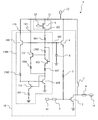
- FIG. 3 shows the first circuit.
- FIG. 3 shows the first circuit 313 indicated by a broken line together with a resistor 104 and a transistor 108 which are peripheral elements.
- 3 is a terminal to which the first resistor 104 is connected (first terminal of the first circuit)
- a terminal 302 is a terminal to which the collector terminal of the first bipolar transistor 108 is connected (first terminal).
- the second terminal of the first circuit ).
- the first circuit 313 includes a transistor 103 and peripheral connections (303 to 307).
- a path from the base terminal of the transistor 103 to the collector terminal of the transistor 103 through the connections 304, 305, and 306 is a first connection path, and a connection with the terminal 301 that is the first terminal is 303.
- the terminal 308 on the first connection path connected by the above becomes the first connection terminal.
- connections 303 to 307 are resistors, and the rest are wiring.
- the first circuit 118 of the voltage generation circuit 101 is the same as the first circuit 313 in FIG. 3 except that the connections 303 and 304 are wirings and the connections 305, 306, and 307 are resistors 105, 106, and 107, respectively. is there.
- the base terminal of the transistor 112 (fourth bipolar transistor) is connected to the terminal 311 of the first connection path.
- the emitter terminal of the transistor 112 (fourth bipolar transistor) is connected to the path from the emitter terminal of the transistor 103 to the collector terminal of the transistor 108 via the connection 307 (in the voltage generation circuit 101, to the collector terminal of the transistor 108).
- the first circuit 313 shown in FIG. 3 generates a voltage for controlling the base terminal of the transistor 114 (second bipolar transistor) of the voltage generation circuit 101 at the terminal 302 (in the voltage generation circuit 101, the collector terminal of the transistor 108). It is a circuit to make. Therefore, it is necessary to provide a circuit that generates the sum of the forward base-emitter junction voltage of the transistor 103 and the voltage drop due to resistance between the first terminal 301 and the second terminal 302 in accordance with the emitter current. Therefore, at least one resistor is required in the path from the first terminal 301 to the connection 303, the connection 304, the base emitter junction of the transistor 103, and the connection 307 to the second terminal 302.
- connection 307 is a resistor
- the emitter current of the transistor 103 flows directly and a voltage drop occurs according to the emitter current.
- almost the same current flows in the connection 303 as in the connection 307. Therefore, if the connection 303 is a resistor, a voltage drop occurs similarly.
- a current of ( ⁇ + 1) of the emitter current flows to the base terminal of the transistor 103, if the connection 304 connected to the base terminal is a resistor, a voltage drop corresponding to the emitter current is also generated.
- the resistance value of the resistance at the position of the connection 304 is set to the position of the connection 303, 307 in order to produce the same voltage drop effect as when the connection 303, 307 is a resistance.
- the resistance value may be ( ⁇ + 1) times as large as the resistance connected to.
- the voltage of the base terminal of the transistor 114 can be controlled as described above. That is, a voltage of Vbe is generated at the base terminal of the transistor 114, and as the emitter current of the transistor 103 is increased (as the power supply voltage is increased), the voltage controlled so that the voltage is decreased due to the voltage drop of the resistor. Can be generated.
- the voltage generation circuit 101 it is necessary to control the voltage between the base and emitter of the transistor 112 so as to be lower than the voltage between the base and emitter of the transistor 103 according to the collector current of the transistor 103.
- at least the potential of the base terminal of the transistor 112 needs to be connected to a terminal that is lower in accordance with the collector current of the transistor 103 than the potential of the first connection terminal 308 to which the base terminal of the transistor 103 is connected. is there.
- As a terminal on the first connection path between the first connection terminal 308 and the collector terminal 311 of the transistor 103 for example, if the base terminal of the transistor 112 is connected to the terminal 311, the first connection terminal 308.
- At least a resistor is required somewhere in the first connection path (connections 305 and 306) between the terminal 311 and the terminal 311. (In the voltage generation circuit 101, both the connections 305 and 306 are resistors.)
- connection 304 is a resistor, the potential of the base terminal of the transistor 103 is lower than the potential of the first connection terminal 308 by the voltage drop of the resistor arranged at the position of the connection 304.
- the “resistance between the base terminal of the transistor 103 and the first connection terminal” is the sum of “resistance of the connection 307” and “1 / ⁇ of the resistance of the connection 304”. The condition that it is set large is necessary.
- the collector current of the transistor 103 sets the voltage between the base and emitter of the transistor 112, which is the fourth bipolar transistor, to be lower than the voltage between the base and emitter of the transistor 103, which is the third bipolar transistor, by the voltage drop of the resistor. Is done. As the collector current increases, the voltage drop increases. As described above, the transistor 112 causes the collector current to flow at a low power supply voltage. However, as the power supply voltage increases, the collector current becomes a maximum value and starts to decrease.
- the base terminal and the emitter terminal of the transistor 112 can be connected to the first connection path and the “path from the emitter terminal of the transistor 103 corresponding to the connection 307 to the collector terminal of the transistor 108” through resistors, respectively.
- the resistance can be adjusted so as to decrease the aforementioned maximum value of the collector current of the transistor 112, or the timing of the power supply voltage at which the maximum value is reached can be adjusted.
- the amount of current can be adjusted by the element size of the transistor 112. Furthermore, you may use combining these structures.
- the collector terminal of the transistor 112 is connected to the power source via the resistor 104, that is, the case where it is connected to the terminal 301, 310 or 311 in FIG.
- the collector current of the transistor 112 flows through the resistor 104, and the voltage drop of the resistor 104 cancels all the effects. End up. Therefore, it is necessary that the collector terminal of the transistor 112 does not pass through at least a part of the resistance element that constitutes the resistor 104 so that all of the above actions are not canceled. Further, it is preferable that the resistor 104 does not exist partly on the connection path between the collector terminal and the power supply terminal of the transistor 112 as in the voltage generation circuit 101.
- a terminal corresponding to the terminal 116 of the voltage generation circuit 101 is a terminal 301.
- the output voltage generated at the terminal 116 is improved by the action of the current flowing through the transistor 112 and the transistor 114, so that a rapid voltage drop on the low power supply voltage side is improved.
- a voltage obtained by reducing the voltage almost in proportion to the increase of the power supply voltage from the above-described improved voltage (the output voltage of the terminal 116) like the terminal 117 in the voltage generation circuit 101.
- a voltage output terminal may be arranged through a resistor on the collector terminal side of the transistor 103 as viewed from the terminal 301.
- such an effect can be obtained by arranging a voltage output terminal with a resistance at any one of the connections 303, 305, and 306 and sandwiching at least one resistance (for example, a resistance at the position of the connection 303) as viewed from the terminal 301. Can be obtained.
- the connection 304 is a resistor
- the terminal 309 on the base side of the transistor 103 across the connection 304 can be used as a voltage output terminal. It is possible to obtain an effect that the output voltage is lowered according to the increase.
- the resistor is usually a large resistor. In that case, the internal resistance as a power source of the voltage generation circuit becomes large, which is not preferable. It is also possible to divide the resistor 104 and use the terminal between them as a voltage output terminal. The output voltage is linear as the power supply voltage is increased with respect to the improved voltage on the low voltage side generated at the terminal 301. An increased output voltage can be obtained.
- connection position of the base terminal of the transistor 112 and the connection position of the voltage output terminal to the first connection path are not particularly required as a mutual relationship and can be selected independently.
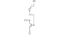
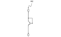
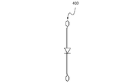
- FIGS. 4A to 4D are diagrams showing other examples of the second circuit.
- the second circuit is intended to generate a forward junction voltage between the first terminal of the first circuit and the base terminal of the first bipolar transistor 108.
- the same configuration as that of a conventional voltage generation circuit for example, the voltage generation circuits 51 and 61 can be used.
- a circuit 401 in FIG. 4A is a schematic diagram of a configuration using transistors shown in the configuration of the voltage generation circuit 101.
- the collector terminal is connected to the power supply, but as described above, the voltage may be equal to or higher than that of the base terminal. Therefore, a configuration in which the collector terminal is connected to the base terminal as in the circuit 402 in FIG. 4B can be employed.
- the circuit 402 When the circuit 402 is regarded as a two-terminal circuit, it has the diode characteristic itself, and thus can be replaced with a diode as in the circuit 403 in FIG. 4C. At this time, the diode may be a circuit in which one terminal of the transistor is not connected in addition to the one using the two terminals of the transistor as in the circuit 402.
- the voltage drop due to the resistance is the voltage at the collector terminal. If it is within the margin range, it operates in the same way as a diode. In this case, the voltage at the collector terminal may be used as another control voltage.
- a resistor is connected in series with a diode that is the second junction element, or a resistor is inserted between the base terminal of the transistor and the circuit, or between the emitter terminal and the circuit.
- the current flowing through the resistor increases and the output voltage increases. Therefore, in many cases, it is not preferable for the purpose of the present invention “to improve the output voltage that gradually increases as the power supply voltage increases”.
- the output voltage that gradually increases with respect to the increase in the power supply voltage can be improved by inserting a resistor. It may be used as one of gender adjustment methods.
- the resistor 111 arranged in the voltage generation circuit 101 is not an essential configuration (an example in which there is no resistor 111 is shown in a circuit described later).
- the presence of the resistor 111 has an effect that current flows through the transistor 109 from an early stage, and the voltage between the base and emitter of the transistor 109 is stabilized early.
- the power supply voltage is low, an excessive increase in the base voltage of the transistor 108 is suppressed, the collector current of the transistor 108 (current flowing through the resistor 104) is suppressed, and the voltage drop of the resistor 104 is reduced to reduce the output voltage. Since the effect is to be increased, there is also an effect that the operation at a lower power supply voltage becomes relatively good.
- a current source such as a diode, a series circuit of a diode and a resistor, a current mirror, or the like may be connected so that current flows from the emitter of the transistor 109 to ground.
- the voltage generation circuit 101 By using the voltage generation circuit 101 according to the present invention, it is possible to provide a voltage generation circuit with improved power supply voltage dependency at a low voltage, and low power supply voltage dependency in a wider range of power supply voltages.
- a voltage generation circuit can be provided.
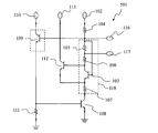
- FIG. 5 is a circuit diagram showing another example of the voltage generating circuit according to the present invention.
- the voltage generation circuit 501 has the same configuration as the voltage generation circuit 101 shown in FIG. 1 except that the second bipolar transistor 114 and the resistor 115 are not provided.
- the action of the currents flowing through the resistor 104 decreasing at the “timing at which the transistor 103 starts flowing the collector current” is caused by the action of the resistors 105 and 106 and the transistor 112. This is to show that the effect of increasing the output voltage on the power supply voltage side is produced.
- the fourth transistor 112 is an element having a quadruple emitter size.
- the resistor 105 is set to 35 ⁇ , and the resistor 106 is set to 165 ⁇ .
- the power supply voltages 102, 110, and 113 are all set to the same potential.
- FIG. 6 is a diagram showing the relationship between the output voltage of the voltage generation circuit shown in FIG. 5 and the power supply voltage.
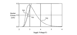
- FIG. 7 is a diagram showing the relationship between the current of each part of the voltage generation circuit shown in FIG. 5 and the power supply voltage.
- a graph curve 601 indicates the relationship between the output voltage and the power supply voltage when the terminal 116 is used as a voltage output terminal in the voltage generation circuit 501.
- a graph curve 602 shows a relationship between an output voltage and a power supply voltage when the terminal 117 is used as a voltage output terminal in the voltage generation circuit 501.
- a graph curve 603 shows a voltage obtained by changing the size of the transistor 109 to an emitter size of 1.9 times so that the output voltage of the terminal 117 when the power supply voltage is 3 V is the same output voltage as that of the conventional voltage generation circuit 51.
- the relationship between the output voltage of the generation circuit 501 and the power supply voltage is shown.
- a graph showing the relationship between the output voltage of the conventional voltage output circuit 51 and the power supply voltage is shown as a graph curve 71.
- the output voltage at the low power supply voltage when the terminal 116 of the voltage generation circuit 501 is a voltage output terminal is higher than the output voltage (graph curve 71) of the conventional voltage generation circuit 51. It is high. As a result, the characteristic that the slope is increased and the output voltage is lowered as the power supply voltage is lowered is improved, and the slope at the power supply voltage of about 3 V or more approaches a straight line.
- the output voltage when the terminal 117 of the voltage generation circuit 501 is used as a voltage output terminal is substantially constant when the power supply voltage is about 3V or more.
- the voltage generation circuit 501 in which the size of the transistor 109 is changed (a model for more accurately comparing the power supply voltage dependency of the output voltage) is also used in the output voltage of the conventional voltage generation circuit 51. It can be confirmed that the power supply voltage dependency is low in a wide range as compared with FIG.
- the operation of the voltage generation circuit 501 according to the present invention will be described below.
- the voltage generation circuit 501 has a configuration in which the transistor 114 and the resistor 115 are removed from the voltage generation circuit 101.
- the current flowing through the resistor 104 is reduced at the “timing at which the transistor 103 starts to flow a collector current”, and the functions of the resistors 105 and 106 and the transistor 112 are reduced. This is to show that the effect of increasing the output voltage on the low power supply voltage side is produced.
- the element size of the transistor 112 is increased in order to increase the function of the transistor 112 because the transistor 114 does not function. *
- a graph curve 701 indicates the relationship between the emitter current of the transistor 103 in the voltage generation circuit 501 and the power supply voltage.
- a graph curve 702 shows the relationship between the emitter current of the transistor 112 and the power supply voltage.
- a graph curve 703 a graph showing the relationship between the emitter current of the third transistor 103 and the power supply voltage in a circuit in which the fourth transistor 112 is removed from the power supply generation circuit 501 is shown.
- the transistor 112 flows an emitter current mainly on the low power supply voltage side. Also, the graph curve 702 is slightly below the graph curve 703. It can be seen that the emitter current of the transistor 103 is relatively decreased from the graph curve 703 to the graph curve 701 by the presence of the transistor 112 that allows current to flow on the low power supply voltage side.
- the decrease in the emitter current of the transistor 103 is smaller than the emitter current of the transistor 112 (graph curve 702). Most of this current is an increase in the collector current of the transistor 108. Then, the emitter current of the transistor 103 (current flowing through the resistor 104) slightly decreases, and the effect of increasing the output voltage on the low voltage side appears due to this action.
- the voltage generation circuit 501 can bring the power supply voltage dependency of the output voltage closer to a linear one by increasing the output voltage on the low power supply voltage side.
- the resistor 105 causes a voltage drop in proportion to the current, so that the voltage at the terminal 116 where the voltage increases linearly is cancelled. It is possible to generate an output voltage that is less dependent on the voltage supply voltage in a wide supply voltage range.
- the voltage generation circuit 501 has a configuration in which the transistor 114 and the resistor 115 of the voltage generation circuit 101 are not provided, and it is not necessary to control the base voltage of the transistor 114. Therefore, it is not necessary for the first circuit 313 to generate a voltage drop between the first terminal 301 and the second terminal 302 due to the forward base-emitter junction voltage and resistance of the transistor 103 according to the emitter current. Therefore, no resistance is required for a path from the first terminal 313 to the second terminal through the connection 303, the connection 304, the base-emitter junction of the transistor 103, and the connection 307. That is, the resistor 107 shown in the voltage generation circuit 501 is not particularly necessary in this embodiment. However, since there is no hindrance to the operation even if there is a resistor, the resistor 107 is left in the voltage generation circuit 501.
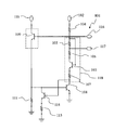
- FIG. 8 is a circuit diagram showing another example of the voltage generating circuit according to the present invention.
- the voltage generation circuit 801 is the same as the voltage generation circuit 101 except that it does not include the transistor 112 that is the fourth bipolar transistor and the power supply terminal 113. Even in the configuration without the terminal 113, an effect that the current flowing through the resistor 104 decreases at the “timing at which the transistor 103 starts flowing the collector current” occurs due to the operation of the resistors 107 and 115 and the transistor 114, and the output voltage on the low power supply voltage side is reduced. This is to show that the effect of increasing produces the effect of appearing.
- the power generation circuit 801 does not have the function of the fourth transistor 112 of the voltage generation circuit 101, so that the function of the transistor 114 which is the second bipolar transistor is strengthened.
- the resistance value of the resistor 107 which was 200 ⁇ , is 50 ⁇ .
- the resistor 105 is 30 ⁇ , and the resistor 106 is 170 ⁇ .
- the power supply voltages 102 and 110 are set to the same potential.
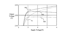
- FIG. 9 is a diagram showing the relationship between the output voltage of the voltage generation circuit shown in FIG. 8 and the power supply voltage.
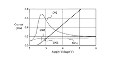
- FIG. 10 is a diagram showing the relationship between the current in each part of the voltage generation circuit shown in FIG. 8 and the power supply voltage.
- the graph curve 901 shows the relationship between the output voltage and the power supply voltage when the terminal 116 of the voltage generation circuit 801 is used as a voltage output terminal.
- a graph curve 902 shows the relationship between the output voltage and the power supply voltage when the terminal 117 of the voltage generation circuit 801 is used as a voltage output terminal.
- a graph curve 903 shows the voltage output of the voltage generation circuit 801 in which the resistance value of the resistor 111 is changed to 24000 ⁇ so that the output voltage of the terminal 117 when the power supply voltage is 3 V becomes the same output voltage as that of the conventional voltage generation circuit 51. And the relationship between the power supply voltage.
- a graph showing the relationship between the output voltage of the conventional voltage output circuit 51 and the power supply voltage is shown as a graph curve 71.
- the output voltage at the low power supply voltage when the terminal 116 of the voltage generation circuit 801 is the voltage output terminal is higher than the output voltage of the conventional voltage generation circuit 51 (graph curve 71). It is high. As a result, the characteristic that the slope is increased and the output voltage is lowered as the power supply voltage is lowered is improved, and the slope at the power supply voltage of about 3 V or more approaches a straight line.
- the output voltage when the terminal 117 of the voltage generation circuit 801 is used as the voltage output terminal is substantially constant when the power supply voltage is about 3V or more.
- the voltage generation circuit 801 (model for comparing the power supply voltage dependency of the output voltage more accurately) in which the resistance value of the resistor 111 is changed is also output from the conventional voltage generation circuit 51. It can be confirmed that the power supply voltage dependency is lower in a wide range than the voltage.
- a graph curve 1001 shown in FIG. 10 is the emitter current of the transistor 103 in the voltage generation circuit 801, and a graph curve 1002 shows the sum of the current flowing through the resistor 111 and the collector current of the transistor 112.
- a graph curve 1003 that is an emitter current of the transistor 103 and a graph curve 1004 that is a current flowing through the resistor 111 when a simulation is performed using a circuit in which only the transistor 114 and the resistor 115 are removed from the voltage generation circuit 801 are also shown. Show.
- the presence of the transistor 114 causes the current (graph curve 1002) flowing to the ground by the transistor 114 and the resistor 111 to be lower than the current (graph curve 1004) without the transistor 114 and only the resistor 111 (graph curve 1004).
- the graph curve 1001 is slightly below the graph curve 1003. It can be seen that the emitter current of the transistor 103 is relatively decreased from the graph curve 1003 to the graph curve 1001 by the presence of the transistor 114 that flows current on the low power supply voltage side. Then, the emitter current of the transistor 103 (current flowing through the resistor 104) slightly decreases, and the effect of increasing the output voltage on the low voltage side appears due to this action.
- the voltage generation circuit 801 can also bring the power supply voltage dependency of the output voltage closer to a linear one by increasing the output voltage on the low power supply voltage side.
- the resistor 105 causes a voltage drop proportional to the current, so that the voltage at the terminal 116 where the voltage increases linearly is canceled and the terminal 117 is wide. It is possible to generate an output voltage that is less dependent on the power supply voltage in the power supply voltage range.
- the voltage generation circuit 801 does not include the transistor 112 and the power supply terminal 113 of the voltage generation circuit 101. Therefore, a condition relating to a position where the base terminal and the emitter terminal of the transistor 112 are connected and a resistance value between the connection terminals for controlling a voltage difference between them is not necessary. That is, the resistor 106 shown in the voltage generation circuit 801 is not particularly necessary.
- the resistor 105 When the voltage output terminal 116 is used without using the voltage output terminal 117, the resistor 105 is not necessary, and the transistor 103 has a configuration in which the base terminal and the collector terminal are connected.
- the circuit can be a series circuit of a diode and a resistor connected in the forward direction. Note that even if there is a resistor at the position of the resistor 106, there is no hindrance to the operation, so the voltage generation circuit 801 shows the resistor 106 remaining.
- the first circuit 313 has a forward base-emitter junction voltage (or forward direction of the transistor 103) between the first terminal 301 and the second terminal 302. It is necessary to generate a voltage drop due to the diode junction voltage) and resistance in accordance with the emitter current (or diode current). Therefore, a resistor is required in at least one of a path from the first terminal to the second terminal via the connection 303, the connection 304, the base-emitter junction of the transistor 103, and the connection 307.
- the other components other than the transistor 112 and the power supply terminal 103 and the adjustment method are the same as those of the circuit 101.
- FIG. 11A is a circuit diagram showing another example of the voltage generating circuit according to the present invention
- FIG. 11B is a circuit diagram showing another example of the voltage generating circuit according to the present invention.
- the voltage generation circuit 1101 and the voltage generation circuit 1102 have a transistor 1103 in which a base terminal and a collector terminal are connected.
- the transistor 1103 can be regarded as a diode having a base terminal as an anode terminal and an emitter terminal as a cathode terminal.
- the diode 1103 (transistor 1103) is the second circuit
- the anode terminal of the diode is the first terminal
- the cathode terminal is the second terminal.
- the terminal 117 is omitted, and the voltage generation circuit has only the terminal 116.
- the transistor 1103 has an emitter size of 1/10.
- the resistors 1104 and 107 are 100 ⁇ , and the resistor 115 is 2000 ⁇ .
- the power supply voltages 102 and 110 have the same potential.
- FIG. 12 is a diagram showing the relationship between the output voltage of the voltage generation circuit shown in FIGS. 11A and 11B and the power supply voltage.
- a graph curve 1201 is a graph showing the relationship between the output voltage of the voltage generation circuit 1101 and the power supply voltage.
- a graph curve 1202 is a graph showing the relationship between the output voltage of the voltage generation circuit 1102 and the power supply voltage.
- a graph showing the relationship between the output voltage of the conventional voltage generation circuit 51 and the power supply voltage is shown as a graph curve 71.
- the second circuit is the diode 1103
- direct comparison with the conventional voltage generation circuit 51 is difficult. Therefore, a configuration without the transistors 112 and 114 and the resistor 115 of the voltage generation circuits 1101 and 1102 (both circuits have the same configuration) is used as a comparison circuit, and the relationship between the voltage output and the power supply voltage is shown as a graph curve 1203. Yes.
- the output voltage on the low power supply voltage side of the above-described comparison circuit is lower than the output voltage of the conventional voltage generation circuit 51. This is because the transistor of the second circuit is replaced with a diode. Therefore, the voltage generation circuits 1101 and 1102 (graph curves 1201 and 1202) having the same second circuit configuration perform the following comparison with respect to the characteristics of the output voltage (graph curve 1203) of the comparison circuit.
- the output voltage at the low power supply voltage of the voltage generation circuit 1101 is higher than the output voltage (graph curve 1203) of the above-described comparison circuit.
- the characteristic that the slope increases and the output voltage decreases as the power supply voltage decreases is improved, and the slope at the power supply voltage of about 3.5 V or more approaches a straight line.
- the output voltage at the low power supply voltage of the voltage generation circuit 1102 is higher than the output voltage (graph curve 1203) of the above-described comparison circuit.
- the characteristic that the slope increases and the output voltage decreases as the power supply voltage decreases is improved, and the slope at the power supply voltage of about 3.5 V or more approaches a straight line.
- the voltage generation circuit 1101 and the voltage generation circuit 1102 have a configuration in which the transistor 109 which is a junction element of the second circuit of the voltage generation circuit 501 and the voltage generation circuit 801 is replaced with a diode 1103 and the resistor 111 is omitted. Yes. Even in such a configuration, there is an effect that the current flowing through the resistor 104 decreases at “timing at which the transistor 103 starts flowing the collector current”. This action is caused by the action of the resistor 1104 and the transistor 112 in the voltage generation circuit 1101 and by the action of the resistors 107 and 115 and the transistor 114 in the voltage generation circuit 1102. This action produces the effect of increasing the output voltage on the low power supply voltage side.
- the transistor 109 in the second circuit of the voltage generation circuit 501 and the voltage generation circuit 801 can be replaced with the diode 1103 and the resistor 111 can be omitted.
- the configuration using the transistor 109 originally has better power supply voltage dependency of the output voltage on the low power supply voltage side than the configuration using the diode 1103. Therefore, the case where the structure of the present invention (the function of the transistors 112 and 114) is combined with the structure of the transistor 109 is more effective than the structure of the diode 1103.
- FIG. 13A is a circuit diagram showing another example of the voltage generating circuit according to the present invention.
- FIG. 13B is a circuit diagram showing a replaceable circuit of the voltage generating circuit shown in FIG. 13A.
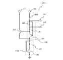
- the voltage generation circuit 1301 has a configuration in which the diode 1103 of the voltage generation circuit 1101 described above is omitted and the base terminal of the transistor 108 is connected to the emitter terminal of the transistor 103 (the terminal 117 is connected to the voltage output). An example of a terminal is also shown).
- the diode 1304 is a diode in which the base terminal of the transistor 108 in which the base terminal and the collector terminal are connected by the resistor 107 is used as an anode terminal and the emitter terminal is used as a cathode terminal.
- the voltage generation circuit 1302 is a circuit equivalent to the voltage generation circuit 1301 in which the above-described diode 1304 is described as a two-terminal diode 1305.
- the diode 1304 and the diode 1305 are the first diodes.
- a simulation using the circuit configuration model of FIGS. 13A and 13B is performed to calculate values such as the output voltage. Note that in the simulation, the element size of the transistor 112 is nine times, the resistance 105 is 70 ⁇ , and the resistance 106 is 130 ⁇ .
- the power supply voltages 102 and 110 are set to the same potential.
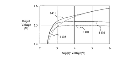
- FIG. 14 is a diagram showing the relationship between the output voltage of the voltage generation circuit shown in FIGS. 13A and 13B and the power supply voltage.
- a graph curve 1401 is a graph showing the relationship between the output voltage and the power supply voltage when the terminal 116 of the voltage generation circuit 1301 is used as a voltage output terminal
- the graph curve 1402 is a voltage at the terminal 117 of the voltage generation circuit 1301. It is a graph which shows the relationship between the output voltage at the time of using as an output terminal, and a power supply voltage.
- a graph curve 1403 for comparison a graph showing the relationship between the output voltage of the comparison circuit excluding the transistor 112 from the voltage generation circuit 1301 and the power supply voltage is shown.
- the graph curve 1404 shows a voltage generation circuit in which the size of the transistor 108 is changed to 2.2 times so that the output voltage of the terminal 117 when the power supply voltage is 3 V is the same as the output voltage of the comparison circuit described above.
- 13 is a graph showing a relationship between an output voltage of a terminal 117 of 1301 and a power supply voltage.
- the output voltage when the terminal 117 of the voltage generation circuit 1301 is used as a voltage output terminal is approximately constant at a power supply voltage of about 3V or more.
- the voltage generation circuit 1301 in which the size of the transistor 108 is changed (a model for more accurately comparing the power supply voltage dependency of the output voltage) is also compared with the output voltage of the comparison circuit described above. It can be confirmed that the power supply voltage dependency is low in a wide range.
- the voltage at the terminal 116 is reduced by the forward junction voltage of the diode 1103 (the forward junction voltage of the base-emitter junction of the transistor constituting the diode 1103). , Applied to the base terminal of the transistor 108.
- the voltage at the terminal 116 is applied to the base terminal of the transistor 1303 as being reduced by the forward junction voltage of the base-emitter junction of the transistor 103. If you think about it, you can see that it works almost the same. That is, the effect that the current flowing through the resistor 104 decreases at the “timing at which the transistor 103 starts to flow the collector current” occurs due to the operation of the resistors 105 and 106 and the transistor 112, and the effect of increasing the output voltage on the low power supply voltage side appears. ing.
- the resistor 105 causes a voltage drop in proportion to the current.
- the resistor 107 is not necessary for operation and can be omitted as in the voltage generation circuit 1101. Further, the operation is possible even if the resistor 107 is provided, and the voltage generation circuit 1301 is shown as a configuration example having a resistor.
- FIG. 15 is a diagram showing another example of the voltage generating circuit according to the present invention.
- a resistor 1502 is connected to the voltage generation circuit 101 between the emitter terminal of the transistor 109 of the voltage generation circuit 101 and the base terminal of the transistor 108 which is the first bipolar transistor.
- a resistor 1503 is connected instead of the resistors 105 and 106 of the first circuit, and the emitter terminal of the transistor 112 which is the fourth bipolar transistor is connected to the collector terminal of the transistor 108 via the resistor 1504. ing. Also, the resistor 111 is omitted.
- the element size of the transistors 114 and 112 is four times, the element size of the transistor 108 is 1.1 times, and the element size of the transistor 109 is 1.5 times.
- the resistance value of the resistor 1502 is 10 ⁇
- the resistance value of the resistor 1503 is 400 ⁇
- the resistance value of the resistor 115 is 130 ⁇
- the resistance value of the resistor 1504 is 200 ⁇
- the resistance value of the resistor 107 is 30 ⁇ .
- the power supply voltages 102, 110, and 113 are set to the same potential.
- FIG. 16A is a diagram showing the relationship between the output voltage and the power supply voltage of the voltage generation circuit according to the present invention
- FIG. 16B is a diagram showing the relationship between the power supply voltage and the output voltage of the voltage generation circuit shown in FIG.
- a graph curve 1601 shows the relationship between the output voltage of the voltage generation circuit 1501 and the power supply voltage
- the graph curve 1602 shows the output voltage of the voltage generation circuit 1501 when a current of 100 ⁇ A is taken out from the voltage output terminal 116.
- the relationship with the power supply voltage is shown.
- a graph showing the relationship between the output voltage of the conventional voltage generation circuit 51 and the power supply voltage is shown as a graph curve 71.
- a graph curve 75 a graph curve showing the relationship between the output voltage of the voltage generation circuit 51 and the power supply voltage when a current of 100 ⁇ A is taken out from the voltage output terminal 57 of the conventional voltage generation circuit 51 is shown.
- a graph curve 203 indicates the relationship between the output voltage and the power supply voltage when the terminal 117 of the voltage generation circuit 101 is used as a voltage output terminal.
- a graph curve 204 shows the relationship between the output voltage and the power supply voltage when a current of 100 ⁇ A is taken from the voltage output terminal 117 of the voltage generation circuit 101.
- FIG. 16B also shows a graph curve 71 and a graph curve 75 as in FIG. 16A.
- the output voltage is almost constant when the power supply voltage is about 2.7 V or more (wide power supply voltage range) even though the terminal 116 is a voltage output terminal. .
- the output voltage (graph curve 204) when current 100 ⁇ A is extracted is lower than the output voltage (graph curve 203) from which current is not extracted.
- the output voltage from which current is not extracted graph curve 1601
- the output voltage when current 100 ⁇ A is extracted There is almost no change between (graph curve 1602) (graph curve 1601 is not lowered with respect to graph curve 1602).
- the voltage generation circuit 1501 has a configuration in which the resistor 111 is omitted from the voltage generation circuit 101. Even in this case, the current flowing through the resistor 104 has an effect of decreasing at “timing at which the transistor 103 starts flowing the collector current”. This action is caused by the action of the resistor 1503, the transistor 112, and further the resistors 107, 115, and the transistor 114, and the effect that the effect of increasing the output voltage on the low power supply voltage side is similarly produced. As described in the embodiment.
- the present embodiment shows that the output voltage can be made constant over a wide power supply voltage range without using a combination with the configuration of the conventional voltage generation circuit 61 (resistor 62).
- the voltage generation circuit 1501 Since the resistor 1502 is an adjustment resistor, the voltage generation circuit 1501 has a configuration in which the resistor 111 is omitted from the voltage generation circuit 101 and the element values of the elements are different from each other. Have.
- the resistor 111 is passing a substantially constant current in a range where the power supply voltage is about 2.5 V or more.
- the current flows so as to gradually decrease the current.
- a current flows through the ground terminal as indicated by a graph curve 1002 as a current obtained by adding both a substantially constant current (graph curve 1004) of the resistor 111 and the transistor 114.
- the maximum value of the current of the transistor 114 is adjusted to be on the lower power supply voltage side, and the collector current gradually decreases when the power supply voltage increases from about 2.6V to about 6V.
- the resistor 111 through which a substantially constant current flows, the setting is made such that the current change of the transistor 114 for the transistor 109 is emphasized.
- the collector 115 of the transistor 114 gradually decreases by increasing the resistance 115, and the current of the transistor 114 decreases as the resistance 115 increases.
- the size is increased.
- the connection of the emitter terminal of the transistor 112 is the lower end of the resistor 107, that is, the collector terminal of the transistor 108.
- the emitter current of the transistor 112 does not pass through the resistor 107, and the base voltage of the transistor 108 is prevented from dropping more than necessary due to the voltage drop of the resistor 107.
- Preventing the base voltage of the transistor 108 from decreasing more than necessary prevents the collector current of the transistor 114 from decreasing more than necessary.
- the size of the transistor 112 is increased to increase the base voltage of the transistor 114 when the power supply voltage is about 2.4 to 2.5 V, that is, “the power supply voltage at which a current starts to flow through the transistor 103”.
- the maximum value of the current of the transistor 114 is adjusted to the lower power supply voltage side.
- the emitter current of the transistor 109 is almost equal to the collector current of the transistor 114, and the emitter current of the transistor 109 is the above transistor 114. It changes in the same way as the collector current. Therefore, when the power supply voltage increases from about 2.6 V to about 6 V, the emitter current of the transistor 109 gradually decreases, and the base-emitter voltage of the transistor 109 gradually decreases.
- the voltage at the voltage output terminal 116 is the sum of the base-emitter voltage of the transistor 108 and the base-emitter voltage of the transistor 109. Therefore, “the operation in which the emitter current of the transistor 108 increases and the base-emitter voltage gradually increases as the power supply voltage increases” is referred to as “the base-emitter voltage of the transistor 109 gradually decreases as the power supply voltage increases. It can be considered that the output voltage is adjusted to a substantially constant value by canceling with the above-mentioned action.
- the voltage generation circuit 1501 since the current flowing through the resistor 1502 also gradually decreases as the power supply voltage increases, the potential difference between both terminals caused by the voltage drop of the resistor 1502 gradually decreases as the power supply voltage increases. This acts as a function of lowering the voltage of the voltage output terminal 116 as the power supply voltage increases.
- the current flowing through the resistor 1502 and the emitter current of the transistor 109 are the same, the change in voltage generated between the terminals of the resistor and between the terminals of the transistor is different for the same current change. It is preferable to adjust so that the voltage becomes flat.
- the size of the transistor 109 is 1.5 times, the resistance 1502 is 10 ⁇ , fine adjustment of power supply voltage dependency is performed, and the size of the transistor 108 is 1.1 times.
- the output voltage when the power supply voltage is 3V is adjusted to be the same value as the conventional voltage generation circuit 51.
- the internal resistance of the voltage generation circuit 1501 looks lower than that of the voltage generation circuit 101 having the terminal 117 as a voltage output terminal. That is, when the current is taken out from the voltage output terminal, the output voltage is hardly lowered. This is because the power generation circuit 101 uses the terminal 117 as a voltage output terminal, so that a current is taken out through the resistor 105. On the other hand, in the voltage generation circuit 1501, there is no resistance corresponding to the resistor 105 because the terminal 116 is a voltage output terminal. Furthermore, as a result of examining the function of the circuit in detail, it was found that not only the presence or absence of the resistor 105 but also the function of the collector current of the transistor 114 is related.
- the functions of the transistors 112 and 114 are not directly caused by changes in the power supply voltage, but are caused by the collector current and emitter current of the transistor 103 as described above. That is, even when a current is taken out from the voltage output terminal and the collector current and the emitter current of the transistor 103 are relatively decreased, the same operation is performed.
- the collector current of the transistor 114 is adjusted so as to gradually decrease to the power supply voltage 6V, the current from the voltage output terminal is extracted in the entire power supply voltage range up to 6V. Therefore, it acts as feedback in the direction of increasing the output voltage.
- the configuration of the present invention is very suitable for combination with the configuration of the conventional voltage generation circuit 61, but the combination with the configuration of the conventional voltage generation circuit 61 is not an essential requirement.
- the configuration of the present embodiment (voltage generation circuit 1501), a voltage generation circuit in which the output voltage is less dependent on the power supply voltage with respect to a wide power supply voltage without a resistor corresponding to the resistor 62 is provided. Is possible.
- the configuration of the present embodiment (voltage generation circuit 1501) can also produce an effect of reducing the internal resistance as a power supply circuit.
- FIG. 17 is a diagram showing an example of a high frequency power amplifier circuit using the voltage generation circuit according to the present invention.
- the high frequency power amplifier circuit 1 includes an amplification transistor 2, an input matching circuit 3, an output matching circuit 4, a ballast resistor 5, a bias transistor 6, a high frequency cutoff choke coil 7, a high frequency signal as a voltage generation circuit.
- the circuit surrounded by the broken line 10 is constituted by an integrated circuit using a heterojunction bipolar transistor (NPN type bipolar transistor), since the transistor element is usually constituted only by an NPN transistor, a PNP type element is required.
- the configuration of the present invention is not important.
- control field effect transistor 9 is configured as a part of the integrated circuit 11 configured by a normally ON type heterojunction field effect transistor.
- a heterojunction field effect transistor is a common component that is often used adjacent to a high-frequency amplifier circuit as a high-frequency switch circuit.
- the power supply voltage applied to the power supply terminal 12 is applied to the collector terminal of the amplification transistor 2 via the choke coil 7.
- the bias transistor 6 has a collector terminal connected to the power supply terminal 12, a base terminal connected to the voltage output terminal 116 of the voltage generation circuit 1501, and a voltage of about 2.5 V is output to the voltage output terminal 116. In such a case, the base current of the amplification transistor 2 is supplied via the ballast resistor 5.
- the control field effect transistor 16 is turned on and off by a signal from the control terminal 13 to change the voltage of the power supply terminal 102 of the voltage generation circuit 1501 to control the operation of the entire circuit.
- the high frequency signal input from the input signal terminal 14 is amplified by the amplification transistor 2 through the input matching circuit 3, and output from the output signal terminal 15 through the output matching circuit 4.
- the circuit Since the voltage applied to the power supply terminal 12 is supplied from a battery in a portable terminal or the like, the circuit needs to operate stably against voltage fluctuations, and the power supply voltage decreases due to battery consumption. Even in this case, it is required to be able to operate up to the lowest possible voltage.
- a constant voltage is generated by a regulator circuit or the like, and a high frequency power amplifier circuit composed of a heterojunction bipolar transistor as an amplifier element is operated.
- the voltage generation circuit of the present invention in which the output voltage dependency on the power supply voltage is small, the voltage fluctuation of the power supply terminal 12 can be achieved even with a simple configuration in which the voltage of the power supply terminal 102 is simply turned on and off by the field effect transistor 9. Therefore, it is possible to provide a high-frequency power amplifier circuit capable of performing a stable amplification operation.
- the field effect transistor 9 is particularly suitable for using a normally ON type field effect transistor. Yes.
- the control field effect transistor 9 is manufactured as a part of the integrated circuit 11 including a high-frequency switch or the like, the high-frequency switch is normally a normally ON type having a pinch-off voltage of about ⁇ 0.5V to ⁇ 1.3V.
- the power supply terminal 102 has “a voltage obtained by multiplying the pinch-off voltage by ⁇ 1”, that is, 0.5V. A voltage of about 1.3V is applied.
- the junction barrier of the junction element is about twice.
- the current does not flow until a voltage of about 4 V or more is applied, and the circuit can be turned off at the above voltage (0.5 V to 1.3 V).
- the voltage generation circuit has two junction elements in all the current paths to the ground terminal as in the circuit 1501, no current flows and unnecessary current consumption is eliminated when the circuit is turned off.
- a current may flow slightly because the current path including the resistor 111 includes only one junction element (transistor 109). Considering the process variation of the integrated circuit, it may be better to use a normally OFF type field effect transistor that can completely cut off the current to the power supply terminal 102 as the control field effect transistor.
- the voltage generation circuit of the present invention it is possible to provide a high-frequency amplifier circuit that can be controlled by simply turning on and off the power supply because a regulator circuit is unnecessary.
- a voltage generation circuit that has two or more junction elements in the current path allows a normally-on field effect transistor to be used for controlling the voltage generation circuit, and a high-frequency amplification capable of operating at a lower power supply voltage.
- a circuit can be provided. In this embodiment, an example of a single-stage amplifier circuit is shown, but a multi-stage amplifier circuit can be similarly configured.
- the present invention can be widely used as a voltage supply source of an electronic circuit that needs to supply a voltage having a small power supply dependency to an output voltage even when the power supply voltage fluctuates, such as a mobile phone and a communication device.
Landscapes
- Engineering & Computer Science (AREA)
- Physics & Mathematics (AREA)
- Microelectronics & Electronic Packaging (AREA)
- Electromagnetism (AREA)
- General Physics & Mathematics (AREA)
- Radar, Positioning & Navigation (AREA)
- Automation & Control Theory (AREA)
- Nonlinear Science (AREA)
- Control Of Electrical Variables (AREA)
- Amplifiers (AREA)
Abstract
Description
図1は、本実施形態に係る電圧発生回路の一例の構成を示す回路図である。図1に示すように、電圧発生回路101は、電源端子102とトランジスタ103のベース端子が抵抗104によって接続されている。また、トランジスタ103のベース端子が抵抗105、106を介してトランジスタ103のコレクタ端子に接続されており、トランジスタ103のエミッタ端子が抵抗107を介してトランジスタ108のコレクタ端子に接続されている。
本発明にかかる電圧発生回路の他の例について図面を参照して説明する。図5は本発明にかかる電圧発生回路の他の例を示す回路図である。
本発明にかかる電圧発生回路のさらに他の例について図面を参照して説明する。図8は本発明にかかる電圧発生回路の他の例を示す回路図である。
本発明にかかる電圧発生回路の他の例について図面を参照して説明する。図11Aは本発明にかかる電圧発生回路の他の例を示す回路図であり、図11Bは本発明にかかる電圧発生回路の他の例を示す回路図である。
本発明にかかる電圧発生回路のさらに他の例について図面を参照して説明する。図13Aは、本発明にかかる電圧発生回路の他の例を示す回路図である。図13Bは、図13Aに示す電圧発生回路の置き換え可能な回路を示す回路図である。
本発明にかかる電圧発生回路のさらに他の例について図面を参照して説明する。図15は本発明にかかる電圧発生回路の他の例を示す図である。
本発明にかかる電圧発生回路を利用した高周波電力増幅回路について図面を参照して説明する。図17は本発明にかかる電圧発生回路を用いた高周波電力増幅回路の一例を示す図である。
102 第1の電源端子
110、113 第1の電源端子と同じ極性の電源端子
103 第3のバイポーラトランジスタ
104 第1の抵抗
105、106、107、111、115 抵抗
108 第1のバイポーラトランジスタ
109 トランジスタ(第2の回路)
112 第4のバイポーラトランジスタ
114 第2のバイポーラトランジスタ
116、117 電力出力端子
118 第1の回路
501 電圧発生回路
801 電圧発生回路
1101、1102 電圧発生回路
1103 ダイオード(第2の回路)
1301、1302 電圧発生回路
1304 第1のダイオード
Claims (4)
- 第1の電源端子と、電圧出力端子と、第1の抵抗と、第1のバイポーラトランジスタと、第2のバイポーラトランジスタと、第1の回路と、第2の回路とを有し、
上記第1の抵抗の第1の端子が、上記第1の電源端子に接続されており、
上記第1のバイポーラトランジスタのエミッタ端子が、接地端子に接続されており、
上記第1の回路の第1の端子が、上記第1の抵抗の第2の端子に接続され、
上記第1の回路の第2の端子が、上記第1のバイポーラトランジスタのコレクタ端子に接続されており、
上記第1の回路が、
ダイオードと抵抗とを有し、上記第1の回路の第1の端子と、上記第1の回路の第2の端子との間に、ダイオード接合の順方向接合電圧と、抵抗による電圧降下との和を、ダイオード電流に応じて発生させる回路、
或いは、
バイポーラトランジスタと抵抗とを有し、上記第1の回路の第1の端子と、上記第1の回路の第2の端子との間に、ベースエミッタ接合の順方向接合電圧と、抵抗による電圧降下との和を、エミッタ電流に応じて発生させる回路、
のいずれかの回路であり、
上記第2の回路の第1の端子が、上記第1の抵抗の第2の端子に接続され、
上記第2の回路の第2の端子が、上記第1のバイポーラトランジスタのベース端子に接続されており、
上記第2の回路が、
ダイオードを有し、上記第2の回路の第1の端子と、上記第2の回路の第2の端子との間に、ダイオード接合の順方向接合電圧を、ダイオード電流に応じて発生させる回路、
或いは、
バイポーラトランジスタを有し、上記第2の回路の第1の端子と、上記第2の回路の第2の端子との間に、ベースエミッタ接合の順方向接合電圧をエミッタ電流に応じて発生させる回路、
のいずれかの回路であり、
上記第2のバイポーラトランジスタのエミッタ端子が、接地端子に接続され、
上記第2のバイポーラトランジスタのコレクタ端子が上記第1のバイポーラトランジスタのベース端子に接続され、
上記第2のバイポーラトランジスタのベース端子が上記第1の回路の第2の端子に接続されており、
上記第1のバイポーラトランジスタのベースエミッタ接合及び上記第2のバイポーラトランジスタのベースエミッタ接合が、上記第1の電源端子の電位に対して順方向に接続され、
上記電圧出力端子が、上記第1の抵抗の第2の端子に直接或いは抵抗を介して接続されていることを特徴とする電圧発生回路。 - 請求項1に記載の電圧発生回路において、第3のバイポーラトランジスタと第4のバイポーラトランジスタとを有し、
上記第3のバイポーラトランジスタのエミッタ端子が、上記第1のバイポーラトランジスタのコレクタ端子に接続され、
上記第3のバイポーラトランジスタのコレクタ端子とベース端子とが第1の接続経路で接続されており、
上記第1の接続経路上に第1の接続端子を有し、
上記第1の接続端子が、上記第1の抵抗の第2の端子に接続され、
上記第4のバイポーラトランジスタのコレクタ端子が、上記第1の電源端子、又は、上記第1の電源端子と同じ極性の電源端子のいずれかに接続され、接続の経路が上記第1の抵抗を構成する抵抗素子の少なくとも一部を含まない接続経路であり、
上記第4のバイポーラトランジスタのエミッタ端子が、上記第3のバイポーラトランジスタのエミッタ端子と上記第1のバイポーラトランジスタのコレクタ端子を接続する接続経路に接続され、
上記第4のバイポーラトランジスタのベース端子が、上記第1の接続端子と上記第3のバイポーラトランジスタのコレクタ端子との間の上記第1の接続経路に、接続されており、
上記第4のバイポーラトランジスタのベース端子と上記第1の接続端子との間の上記第1の接続経路が抵抗を有し、
上記第4のバイポーラトランジスタのベースエミッタ間電圧が、上記第3のバイポーラトランジスタのベースエミッタ間電圧より低くなるように、上記第4のバイポーラトランジスタのベース端子と上記第1の接続端子との間の上記第1の接続経路の抵抗の抵抗値が設定されていることを特徴とする請求項1に記載の電圧発生回路 - 第1の電源端子と、電圧出力端子と、第1の抵抗と、第1のバイポーラトランジスタと、第2のバイポーラトランジスタと、第3のバイポーラトランジスタと、第4のバイポーラトランジスタと、第2の回路とを有し、
上記第1の抵抗の第1の端子が、上記第1の電源端子に接続されており、
上記第1のバイポーラトランジスタのエミッタ端子が、接地端子に接続されており、
上記第3のバイポーラトランジスタのエミッタ端子が、上記第1のバイポーラトランジスタのコレクタ端子に接続され、
上記第3のバイポーラトランジスタのコレクタ端子とベース端子とが第1の接続経路で接続されており、
上記第1の接続経路上に第1の接続端子を有し、
上記第1の接続端子が、上記第1の抵抗の第2の端子に接続され、
上記第4のバイポーラトランジスタのコレクタ端子が、上記第1の電源端子、又は、上記第1の電源端子と同じ極性の電源端子のいずれかに接続され、接続の経路に、上記第1の抵抗を構成する抵抗素子の少なくとも一部を含まず、
上記第4のバイポーラトランジスタのエミッタ端子が、上記第3のバイポーラトランジスタのエミッタ端子と上記第1のバイポーラトランジスタのコレクタ端子を接続する接続経路に接続され、
上記第4のバイポーラトランジスタのベース端子が、上記第1の接続端子と上記第3のバイポーラトランジスタのコレクタ端子との間の上記第1の接続経路に、接続されており、
上記第4のバイポーラトランジスタのベース端子と上記第1の接続端子との間の上記第1の接続経路が抵抗を有し、
上記第4のバイポーラトランジスタのベースエミッタ間電圧が、上記第3のバイポーラトランジスタのベースエミッタ間電圧より低くなるように、上記第4のバイポーラトランジスタのベース端子と上記第1の接続端子との間の上記第1の接続経路の抵抗の抵抗値が設定されており、
上記第2の回路の第1の端子が、上記第1の抵抗の第2の端子に接続され、
上記第2の回路の第2の端子が、上記第1のバイポーラトランジスタのベース端子に接続されており、
上記第2の回路が、
ダイオードを有し、上記第2の回路の第1の端子と、上記第2の回路の第2の端子との間に、ダイオード接合の順方向接合電圧を、ダイオード電流に応じて発生させる回路、
或いは、
バイポーラトランジスタを有し、上記第2の回路の第1の端子と、上記第2の回路の第2の端子との間に、ベースエミッタ接合の順方向接合電圧をエミッタ電流に応じて発生させる回路、
のいずれかの回路であり、
上記第1のバイポーラトランジスタのベースエミッタ接合と、上記第3のバイポーラトランジスタのベースエミッタ接合と、上記第4のバイポーラトランジスタのベースエミッタ接合とのいずれもが、上記第1の電源端子の電位に対して順方向に接続され、
上記電圧出力端子が、上記第1の抵抗の第2の端子に直接或いは抵抗を介して接続されていることを特徴とする電圧発生回路。 - 第1の電源端子と、電圧出力端子と、第1の抵抗と、第1のダイオードとを有し、
上記第1の抵抗の第1の端子が、上記第1の電源端子に接続されており、
上記第1のダイオードの第1の端子が、接地端子に接続されており、
上記第3のバイポーラトランジスタのエミッタ端子が、上記第1のダイオードの第2の端子に接続され、
上記第3のバイポーラトランジスタのコレクタ端子とベース端子とが第1の接続経路で接続されており、
上記第1の接続経路上に第1の接続端子を有し、
上記第1の接続端子が、上記第1の抵抗の第2の端子に接続され、
上記第4のバイポーラトランジスタのコレクタ端子が、上記第1の電源端子、又は、上記第1の電源端子と同じ極性の電源端子のいずれかに接続され、接続の経路に、上記第1の抵抗を構成する抵抗素子の少なくとも一部を含まず、
上記第4のバイポーラトランジスタのエミッタ端子が、上記第3のバイポーラトランジスタのエミッタ端子と上記第1のバイポーラトランジスタのコレクタ端子を接続する接続経路に接続され、
上記第4のバイポーラトランジスタのベース端子が、上記第1の接続端子と上記第3のバイポーラトランジスタのコレクタ端子との間の上記第1の接続経路に、接続されており、
上記第4のバイポーラトランジスタのベース端子と上記第1の接続端子との間の上記第1の接続経路が抵抗を有し、
上記第4のバイポーラトランジスタのベースエミッタ間電圧が、上記第3のバイポーラトランジスタのベースエミッタ間電圧より低くなるように、上記第4のバイポーラトランジスタのベース端子と上記第1の接続端子との間の上記第1の接続経路の抵抗の抵抗値が設定されており、
上記第1のダイオードのダイオード接合と、上記第3のバイポーラトランジスタのベースエミッタ接合と上記第4のバイポーラトランジスタのベースエミッタ接合とのいずれもが、上記第1の電源端子の電位に対して順方向に接続され、
上記電圧出力端子が、上記第1の抵抗の第2の端子に直接或いは抵抗を介して接続されていることを特徴とする電圧発生回路。
Priority Applications (2)
| Application Number | Priority Date | Filing Date | Title |
|---|---|---|---|
| US14/892,253 US20160091910A1 (en) | 2013-06-27 | 2014-06-11 | Voltage generation circuit |
| JP2015523968A JPWO2014208339A1 (ja) | 2013-06-27 | 2014-06-11 | 電圧発生回路 |
Applications Claiming Priority (2)
| Application Number | Priority Date | Filing Date | Title |
|---|---|---|---|
| JP2013135116 | 2013-06-27 | ||
| JP2013-135116 | 2013-06-27 |
Publications (1)
| Publication Number | Publication Date |
|---|---|
| WO2014208339A1 true WO2014208339A1 (ja) | 2014-12-31 |
Family
ID=52141683
Family Applications (1)
| Application Number | Title | Priority Date | Filing Date |
|---|---|---|---|
| PCT/JP2014/065491 Ceased WO2014208339A1 (ja) | 2013-06-27 | 2014-06-11 | 電圧発生回路 |
Country Status (3)
| Country | Link |
|---|---|
| US (1) | US20160091910A1 (ja) |
| JP (1) | JPWO2014208339A1 (ja) |
| WO (1) | WO2014208339A1 (ja) |
Citations (6)
| Publication number | Priority date | Publication date | Assignee | Title |
|---|---|---|---|---|
| JPS5221648A (en) * | 1975-08-12 | 1977-02-18 | Toshiba Corp | Constant-voltage circuit |
| JPS58166412A (ja) * | 1982-03-10 | 1983-10-01 | エヌ・ベ−・フイリツプス・フル−イランペンフアブリケン | 電流識別回路 |
| JPS60129818A (ja) * | 1983-12-19 | 1985-07-11 | Matsushita Electric Ind Co Ltd | 基準電圧回路 |
| JPS63281505A (ja) * | 1987-05-14 | 1988-11-18 | Nippon Telegr & Teleph Corp <Ntt> | 複合型半導体定電圧発生回路装置 |
| JPH02178716A (ja) * | 1988-12-28 | 1990-07-11 | Toshiba Corp | 電圧発生回路 |
| JPH0415716A (ja) * | 1990-05-01 | 1992-01-21 | Sumitomo Electric Ind Ltd | 定電圧源回路 |
Family Cites Families (11)
| Publication number | Priority date | Publication date | Assignee | Title |
|---|---|---|---|---|
| US3629692A (en) * | 1971-01-11 | 1971-12-21 | Rca Corp | Current source with positive feedback current repeater |
| US4639896A (en) * | 1984-11-30 | 1987-01-27 | Harris Corporation | Redundant row decoding for programmable devices |
| JP3322685B2 (ja) * | 1992-03-02 | 2002-09-09 | 日本テキサス・インスツルメンツ株式会社 | 定電圧回路および定電流回路 |
| US5448174A (en) * | 1994-08-25 | 1995-09-05 | Delco Electronics Corp. | Protective circuit having enhanced thermal shutdown |
| US6023185A (en) * | 1996-04-19 | 2000-02-08 | Cherry Semiconductor Corporation | Temperature compensated current reference |
| US5828329A (en) * | 1996-12-05 | 1998-10-27 | 3Com Corporation | Adjustable temperature coefficient current reference |
| US6879214B2 (en) * | 2002-09-20 | 2005-04-12 | Triquint Semiconductor, Inc. | Bias circuit with controlled temperature dependence |
| US7064614B2 (en) * | 2004-07-09 | 2006-06-20 | Xindium Technologies, Inc. | Current mirror biasing circuit with power control for HBT power amplifiers |
| JP4519659B2 (ja) * | 2005-01-06 | 2010-08-04 | ルネサスエレクトロニクス株式会社 | バイアス回路 |
| US8228122B1 (en) * | 2009-06-05 | 2012-07-24 | EpicCom, Inc. | Regulator and temperature compensation bias circuit for linearized power amplifier |
| JPWO2014200027A1 (ja) * | 2013-06-12 | 2017-02-23 | シャープ株式会社 | 電圧発生回路 |
-
2014
- 2014-06-11 JP JP2015523968A patent/JPWO2014208339A1/ja active Pending
- 2014-06-11 WO PCT/JP2014/065491 patent/WO2014208339A1/ja not_active Ceased
- 2014-06-11 US US14/892,253 patent/US20160091910A1/en not_active Abandoned
Patent Citations (6)
| Publication number | Priority date | Publication date | Assignee | Title |
|---|---|---|---|---|
| JPS5221648A (en) * | 1975-08-12 | 1977-02-18 | Toshiba Corp | Constant-voltage circuit |
| JPS58166412A (ja) * | 1982-03-10 | 1983-10-01 | エヌ・ベ−・フイリツプス・フル−イランペンフアブリケン | 電流識別回路 |
| JPS60129818A (ja) * | 1983-12-19 | 1985-07-11 | Matsushita Electric Ind Co Ltd | 基準電圧回路 |
| JPS63281505A (ja) * | 1987-05-14 | 1988-11-18 | Nippon Telegr & Teleph Corp <Ntt> | 複合型半導体定電圧発生回路装置 |
| JPH02178716A (ja) * | 1988-12-28 | 1990-07-11 | Toshiba Corp | 電圧発生回路 |
| JPH0415716A (ja) * | 1990-05-01 | 1992-01-21 | Sumitomo Electric Ind Ltd | 定電圧源回路 |
Also Published As
| Publication number | Publication date |
|---|---|
| JPWO2014208339A1 (ja) | 2017-02-23 |
| US20160091910A1 (en) | 2016-03-31 |
Similar Documents
| Publication | Publication Date | Title |
|---|---|---|
| US9817415B2 (en) | Wide voltage range low drop-out regulators | |
| CN104238613B (zh) | 一种数字电路低压差线性稳压器 | |
| TWI437403B (zh) | Voltage regulator | |
| US7009453B2 (en) | Bias current supply circuit and amplification circuit | |
| TWI780282B (zh) | 過電流限制電路、過電流限制方法及電源電路 | |
| JP2018073288A (ja) | ボルテージレギュレータ | |
| JP4552569B2 (ja) | 定電圧電源回路 | |
| JPWO2014200027A1 (ja) | 電圧発生回路 | |
| KR102225714B1 (ko) | 볼티지 레귤레이터 | |
| WO2014208339A1 (ja) | 電圧発生回路 | |
| CN101552598A (zh) | 切换式功率晶体管的栅极驱动电路 | |
| CN111580593B (zh) | 具有限流电路的多级放大电路 | |
| CN109450395B (zh) | 非线性反馈电路及采用其的低噪声放大器 | |
| TW201339784A (zh) | 穩壓電路及電子裝置 | |
| KR101208035B1 (ko) | 전력증폭기의 바이어스 회로 | |
| JP4712398B2 (ja) | 半導体装置 | |
| KR102163048B1 (ko) | 전력 증폭기 및 전력 증폭기의 전류 제한 방법 | |
| CN112327985B (zh) | 一种低压差线性稳压电路、低压差线性稳压器及电子芯片 | |
| JP2008172538A (ja) | バイアス回路および電力増幅器 | |
| CN109613949B (zh) | 低压降稳压器 | |
| CN116449906B (zh) | 一种稳压器的控制电路、pcb板以及稳压器 | |
| CN118760324B (zh) | 一种无片外电容的线性稳压器、芯片及电子设备 | |
| JP2006127093A (ja) | 定電圧レギュレータ回路 | |
| JP2014241091A (ja) | 電圧発生回路 | |
| JP2025015967A (ja) | 電力増幅装置 |
Legal Events
| Date | Code | Title | Description |
|---|---|---|---|
| 121 | Ep: the epo has been informed by wipo that ep was designated in this application |
Ref document number: 14818173 Country of ref document: EP Kind code of ref document: A1 |
|
| ENP | Entry into the national phase |
Ref document number: 2015523968 Country of ref document: JP Kind code of ref document: A |
|
| WWE | Wipo information: entry into national phase |
Ref document number: 14892253 Country of ref document: US |
|
| NENP | Non-entry into the national phase |
Ref country code: DE |
|
| 122 | Ep: pct application non-entry in european phase |
Ref document number: 14818173 Country of ref document: EP Kind code of ref document: A1 |